Embed Size (px)
Citation preview

SQFlash mSATA 630
Specifications subject to change without notice, contact your sales representatives for the most update information.
REV 0.5 Page 1 of 25 Jun. 8, 2015
mSATA 630 Datasheet
(SQF-SMSxx-xG-S9x)

SQFlash mSATA 630
Specifications subject to change without notice, contact your sales representatives for the most update information.
REV 0.5 Page 2 of 25 Jun. 8, 2015
CONTENTS 1. Overview ............................................................................................ 4
2. Features ............................................................................................. 5
3. Specification Table ............................................................................ 6
4. General Description .......................................................................... 8
5. Pin Assignment and Description ................................................... 10
5.1 mSATA Interface Pin Assignments ................................................................................ 10
6. Identify Device Data ........................................................................ 12
7. ATA Command Set .......................................................................... 16
8. System Power Consumption ......................................................... 22
8.1 Supply Voltage .............................................................................................................. 22
8.2 Power Consumption ...................................................................................................... 22
9. Physical Dimension ........................................................................ 23
Appendix: Part Number Table ........................................................... 24

SQFlash mSATA 630
Specifications subject to change without notice, contact your sales representatives for the most update information.
REV 0.5 Page 3 of 25 Jun. 8, 2015
Revision History
Rev. Date History
0.1 2014/2/17 1. 1st draft
0.2 2014/04/03 1. Update information
0.3 2014/12/25 1. Add 1-CH 8G MLC
0.4 2015/2/6 1. Update write protect pin description
0.5 2015/6/8 1. Correct the description of Write Protect jumper
Advantech reserves the right to make changes without further notice to any products or data herein to improve reliability, function, or
design. Information furnished by Advantech is believed to be accurate and reliable. However, Advantech does not assure any liability
arising out of the application or use of this information, nor the application or use of any product or circuit described herein, neither
does it convey any license under its patent rights nor the rights of others.
Copyright © 1983-2010 Advantech Co., Ltd. All rights reserved.

SQFlash mSATA 630
Specifications subject to change without notice, contact your sales representatives for the most update information.
REV 0.5 Page 4 of 25 Jun. 8, 2015
1. Overview
Advantech SQFlash 630 series mSATA delivers all the advantages of Flash Disk technology with the Serial
ATA III (6.0Gb) interface, fully compliant with standard mSATA form factor. The SQF-SMS is based on the mSATA
form factor which is generated by JEDEC and could provide a wide range capacity from 1GB to 32GB for SLC,
2GB to up to 64GB for Ultra MLC, and 4GB to up to 128GB for MLC. Also it can reach more than 480MB/s read as
well as 180MB/s write high performance even based on MLC flash. The power consumption of Flash Disk is also
much lower than traditional Hard Drive.

SQFlash mSATA 630
Specifications subject to change without notice, contact your sales representatives for the most update information.
REV 0.5 Page 5 of 25 Jun. 8, 2015
2. Features
Standard SATA interface
– Support SATA 1.5/3.0/6.0 Gbps interface
– SATA Revision 3.0 compliant
Operating Voltage:3.3V
Support 72 bit ECC correct per 1K Byte data
TRIM、AHCI supported
Hardware write protect supported
– Pin header type: default on short position for write protect disable
Temperature Ranges
– Commercial Temperature
● 0℃ to 70℃ for operating
● -40℃ to 85℃ for storage
– Industrial Temperature
● -40℃ to 85℃ for operating
● -40℃ to 85℃ for storage
Mechanical Specification
– Shock:1,500G / 0.5ms
– Vibration:20G / 80~2,000Hz
Humidty
– Humidity:5% ~ 95% under 55℃
Endurance : > 2,000,000 program/erase cycles
– This is a test result of the whole SQFlash drive. The test is to keep writing a fixed logical block address
(LBA) and see if any bad blocks occur after 2M cycles. With wear-levelling mechanism, although the disk
was kept writing the same LBA but the physical block changes per block writing. So this test also proves
that wear-leveling is really working, or the block would be wearout after its designated life cycles.
Data Retention
– 10 years
Acquired RoHS、WHQL、CE、FCC Certificate
Acoustic:0 dB
Dimension:50.8 mm x 30.0 mm x 4.2 mm

SQFlash mSATA 630
Specifications subject to change without notice, contact your sales representatives for the most update information.
REV 0.5 Page 6 of 25 Jun. 8, 2015
3. Specification Table
Performance
Sequential Performance (MB/sec) Random Performance (IOPS @4K)
Read Write Read Write
SLC
1 GB 33.83 21.16 6,994 2,533
2 GB 67.44 41.19 13,652 4,531
4 GB 133.40 90.05 20,987 14,687
8 GB 286.40 86.94 40,832 18,468
16 GB 523.00 153.00 36,608 27,392
32 GB 503.70 148.00 41,779 27,238
64 GB 509.50 152.20 36,762 27,418
Ultra MLC
2 GB 153.10 52.93 24,105 8,609
4 GB 301.20 96.34 43,366 18,381
8 GB 310.00 100.00 42,000 23,726
16 GB 495.40 160.50 46,797 27,930
32 GB 491.80 185.60 39,450 24,072
64 GB 488.50 182.80 33,178 16,399
128 GB 524.10 196.70 36,147 27,904
MLC
4 GB 150.40 49.93 22,612 4,155
8 GB (1CH) 123.60 41.98 20,728 9,392
8 GB (2CH) 290.00 97.24 41,037 7,414
16 GB 522.10 184.10 48,410 28,698
32 GB 484.60 153.80 46,797 28,083
64 GB 484.70 194.30 39,757 24,527
128 GB 482.80 182.90 33,152 24,000
256 GB 514.90 193.80 36,122 27,341
* All performance above are tested with AHCI mode.

SQFlash mSATA 630
Specifications subject to change without notice, contact your sales representatives for the most update information.
REV 0.5 Page 7 of 25 Jun. 8, 2015
Endurance According to JEDEC subcommittee JC-64.8, the actual endurance of flash storage can be presented by
Terabyte Write (TBW), which is measured by NAND Flash physical endurance, Wear-leveling Efficiency
(WLE) and Write Amplification Factor (WAF) of specific capacities with following formula.
TBW = [(NAND Flash Physical Endurance) x Capacity x WLE] / WAF
TBW of sequential writing
WLE WAF TBW
SLC Ultra MLC MLC
1 GB 0.9130 1.1013 80 -- --
2 GB 0.9130 1.1017 161 32 --
4 GB 0.9130 1.1025 323 64 9
8 GB 0.9120 1.1026 646 129 19
16 GB 0.9120 1.1031 1291 258 38
32 GB 0.9120 1.1029 2584 516 77
64 GB 0.9110 1.1039 5157 1031 154
128 GB 0.9110 1.1039 -- 2603 309
256 GB 0.9100 1.1041 -- -- 618
TBW of random writing
WLE WAF TBW
SLC Ultra MLC MLC
1 GB 0.9130 1.2176 73 -- --
2 GB 0.9130 1.2837 138 27 --
4 GB 0.9130 1.3034 273 54 8
8 GB 0.9120 1.3278 536 107 16
16 GB 0.9120 2.2323 638 127 19
32 GB 0.9120 2.3535 1210 242 36
64 GB 0.9110 2.4396 2333 466 70
128 GB 0.9110 2.3141 -- 984 147
256 GB 0.9100 2.2614 -- -- 301

SQFlash mSATA 630
Specifications subject to change without notice, contact your sales representatives for the most update information.
REV 0.5 Page 8 of 25 Jun. 8, 2015
4. General Description
Advanced NAND Flash Controller Advantech SQFlash 630 series mSATA includes Bad Block Management Algorithm, Wear Leveling Algorithm,
Error Detection / Correction Code (EDC/ECC) Algorithm, Fragment Writing Technology, and
GuaranteedFlush Technology.
Bad Block Management Bad blocks are blocks that contain one or more invalid bits of which the reliability is not guaranteed. Bad
blocks may be representing when flash is shipped and may developed during life time of the device.
Advantech SQFlash 630 series mSATA implement an efficient bad block management algorithm to detect
the factory produced bad blocks and manages any bad blocks that may develop over the life time of the
device. This process is completely transparent to the user, user will not aware of the existence of the bad
blocks during operation.
Wear Leveling NAND Type flash have individually erasable blocks, each of which can be put through a finite number of
erase cycles before becoming unreliable. It means after certain cycles for any given block, errors can be
occurred in a much higher rate compared with typical situation. Unfortunately, in the most of cases, the flash
media will not been used evenly. For certain area, like file system, the data gets updated much frequently
than other area. Flash media will rapidly wear out in place without any rotation.
Wear leveling attempts to work around these limitations by arranging data so that erasures and re-writes are
distributed evenly across the full medium. In this way, no single sector prematurely fails due to a high
concentration of program/erase cycles.
Advantech SQFlash 630 series mSATA provides advanced wear leveling algorithm, which can efficiently
spread out the flash usage through the whole flash media area. By implement both dynamic and static wear
leveling algorithms, the life expectancy of the flash media can be improved significantly.
Error Detection / Correction Advantech SQFlash 630 series mSATA utilizes BCH ECC Algorithm which offers one of the most powerful
ECC algorithms in the industry. This algorithm can support 72 bit ECC correct per 1K Byte data.
Hardware Write Protect Pin A 2-pin header is mounted and connected to controller reserved GPIO for the drive write protection. When
the pins are opened, all of the write command will be carried to a buffer area without real programming to the
Flash IC. So the data won’t be saved in this mode and will be totally discarded upon power shutting down.
Sophisticate Product Management Systems Since industrial application require much more reliable devices compare with consumer product, a more
sophisticated product management system become necessary for industrial customer requirement. The key
to providing reliable devices is product traceability and failure analysis system. By implement such systems
end customer can expect much more reliable product.
SQFlash mSATA 630
Specifications subject to change without notice, contact your sales representatives for the most update information.
REV 0.5 Page 9 of 25 Jun. 8, 2015
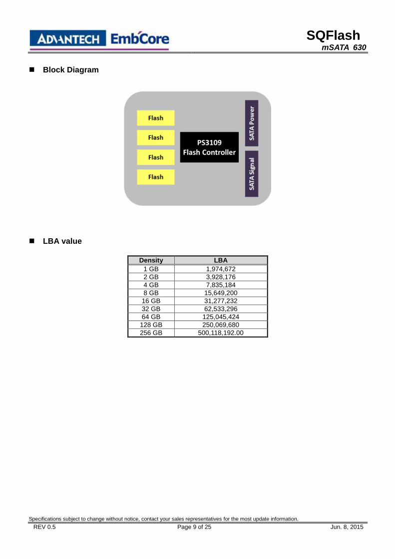
Block Diagram
LBA value
Density LBA
1 GB 1,974,672
2 GB 3,928,176
4 GB 7,835,184
8 GB 15,649,200
16 GB 31,277,232
32 GB 62,533,296
64 GB 125,045,424
128 GB 250,069,680
256 GB 500,118,192.00

SQFlash mSATA 630
Specifications subject to change without notice, contact your sales representatives for the most update information.
REV 0.5 Page 10 of 25 Jun. 8, 2015
5. Pin Assignment and Description
5.1 mSATA Interface Pin Assignments
Pin # Function Description
1 NC No Connect 2 +3.3V 3.3V Source 3 NC No Connect 4 DGND Digital GND 5 NC No Connect 6 NC No Connect 7 NC No Connect 8 NC No Connect 9 DGND Digital GND
10 NC No Connect 11 NC No Connect 12 NC No Connect 13 NC No Connect 14 NC No Connect 15 DGND Digital GND 16 NC No Connect
17 NC No Connect 18 DGND Digital GND 19 NC No Connect 20 NC No Connect 21 SATA GND SATA Ground Return Pin 22 NC No Connect 23 B+ Host Receiver Differential Signal Pair 24 +3.3V 3.3V Source 25 B- Host Receiver Differential Signal Pair 26 SATA GND SATA Ground Return Pin 27 SATA GND SATA Ground Return Pin 28 NC No Connect 29 SATA GND SATA Ground Return Pin 30 NC No Connect 31 A- Host Transmitter Differential Signal Pair 32 NC No Connect 33 A+ Host Transmitter Differential Signal Pair 34 DGND Digital GND 35 SATA GND SATA Ground Return Pin 36 NC No Connect 37 SATA GND SATA Ground Return Pin 38 NC No Connect 39 +3.3V 3.3V Source 40 DGND Digital GND 41 +3.3V 3.3V Source 42 NC No Connect 43 NC No Connect 44 DEVSLP Enter/Exit DevSleep 45 NC Reserved pin 46 NC No Connect

SQFlash mSATA 630
Specifications subject to change without notice, contact your sales representatives for the most update information.
REV 0.5 Page 11 of 25 Jun. 8, 2015
47 NC Reserved pin 48 NC No Connect 49 DA/DSS Device Activity Signal 50 DGND Digital GND 51 GND Default connect to GND 52 +3.3V 3.3V Source

SQFlash mSATA 630
Specifications subject to change without notice, contact your sales representatives for the most update information.
REV 0.5 Page 12 of 25 Jun. 8, 2015
6. Identify Device Data The Identity Device Data enables Host to receive parameter information from the device. The parameter
words in the buffer have the arrangement and meanings defined in below table. All reserve bits or words
are zero
Word Address
Default Value
Data Field Type Information
0 0040h General configuration bit-significant information
1 *1 Obsolete – Number of logical cylinders
2 C837h Specific configuration
3 0010h Obsolete – Number of logical heads (16)
4-5 0000h Retired
6 003Fh Obsolete – Number of logical sectors per logical track (63)
7-8 0000h Reserved for assignment by the Compact Flash Association
9 0000h Retired
10-19 Varies Serial number (20 ASCII characters)
20-21 0000h Retired
22 0000h Obsolete
23-26 Varies Firmware revision (8 ASCII characters)
27-46 Varies Model number (xxxxxxxx)
47 8010h 7:0- Maximum number of sectors transferred per interrupt on MULTIPLE commands
48 4000h Trusted Computing feature set options(not support)
49 2F00h Capabilities
50 4000h Capabilities
51-52 00000h Obsolete
53 0007h Words 88 and 70:64 valid
54 *1 Obsolete – Number of logical cylinders
55 0010h Obsolete – Number of logical heads (16)
56 003Fh Obsolete – Number of logical sectors per track (63)
57-58 *2 Obsolete – Current capacity in sectors
59 0110h Number of sectors transferred per interrupt on MULTIPLE commands
60-61 *3 Maximum number of sector ( 28bit LBA mode)
62 0000h Obsolete
63 0407h Multi-word DMA modes supported/selected
64 0003h PIO modes supported
65 0078h Minimum Multiword DMA transfer cycle time per word
66 0078h Manufacturer’s recommended Multiword DMA transfer cycle time
67 0078h Minimum PIO transfer cycle time without flow control
68 0078h Minimum PIO transfer cycle time with IORDY flow control

SQFlash mSATA 630
Specifications subject to change without notice, contact your sales representatives for the most update information.
REV 0.5 Page 13 of 25 Jun. 8, 2015
69 0100h Additional Supported (support download microcode DMA)
70 0000h Reserved
71-74 0000h Reserved for the IDENTIFY PACKET DEVICE command
75 001Fh Queue depth
76 670eh Serial SATA capabilities
77 0084h Serial ATA Additional Capabilities
78 014Ch Serial ATA features supported
79 0040h Serial ATA features enabled
80 07F8h Major Version Number
81 0000h Minor Version Number
82 346bh Command set supported
83 7d09h Command set supported
84 6063h Command set/feature supported extension
85 3469h Command set/feature enabled
86 bc01h Command set/feature enabled
87 6063h Command set/feature default
88 003Fh Ultra DMA Modes
89 0001h Time required for security erase unit completion
90 001Eh Time required for Enhanced security erase completion
91 0000h Current advanced power management value
92 FFFEh Master Password Revision Code
93 0000h Hardware reset result. The contents of the bits (12:0) of this word can be changed only during the execution of hardware reset.
94 0000h Vendor’s recommended and actual acoustic management value
95 0000h Stream Minimum Request Size
96 0000h Streaming Transfer Time – DMA
97 0000h Streaming Access Latency – DMA and PIO
98-99 0000h Streaming Performance Granularity
100-103 *4 Maximum user LBA for 48 bit Address feature set
104 0000h Streaming Transfer Time – PIO
105 0008h Maximum number of 512-byte blocks per DATA SET MANAGEMENT command
106 4000h Physical sector size/Logical sector size
107 0000h Inter-seek delay for ISO-7779 acoustic testing in microseconds
108-111 0000h Unique ID
112-116 0000h Reserved
117-118 0000h Words per logical Sector
119 4014h Supported settings

SQFlash mSATA 630
Specifications subject to change without notice, contact your sales representatives for the most update information.
REV 0.5 Page 14 of 25 Jun. 8, 2015
120 4014h Command set/Feature Enabled/Supported
121-126 0000h Reserved
127 0000h Removable Media Status Notification feature set support
128 0021h Security status
129-140 0000h Vendor specific
141 0001h Vendor specific
142-159 0000h Vendor specific
160 0000h Compact Flash Association (CFA) power mode 1
161-167 0000h Reserved for assignment by the CFA
168
3h 2.5 inch 4h 1.8 inch
5h Less than 1.8 inch
Device Nominal Form Factor
169 0001h DATA SET MANAGEMENT command is supported
170-173 0000h Additional Product Identifier
174-175 0000h Reserve
176-205 0000h Current media serial number
206 0000h SCT Command Transport
207-208 0000h Reserved
209 4000h Alignment of logical blocks within a physical block
210-211 0000h Write-Read-Verify Sector Count Mode 3 (not support)
212-213 0000h Write-Read-Verify Sector Count Mode 2 (not support)
214-216 0000h NV Cache relate (not support)
217 0001h Non-rotating media device
218 0000h Reserved
219 0000h NV Cache relate (not support)
220 0000h Write read verify feature set current mode
221 0000h Reserved
222 107Fh Transport major version number
223 0000h Transport minor version number
224-229 0000h reserved
230-233 0000h Extend number of user addressable sectors
234 0001h Minimum number of 512-byte data blocks per DOWNLOAD MICROCODE command for mode 03h
235 0080h Maximum number of 512-byte data blocks per DOWNLOAD MICROCODE command for mode 03h
236-254 0000h Reserved
255 XXA5h XX is
variable Integrity word (Checksum and Signature)
Capacity (GB) *1 (Word 1 / 54) *2 (Word 57 - 58) *3 (Word 60 - 61) *4 (Word 100 – 103)
1 7A7h 1E2190h 1E2190h 1E2190h
2 F39h 3BF070h 3BF070h 3BF070h

SQFlash mSATA 630
Specifications subject to change without notice, contact your sales representatives for the most update information.
REV 0.5 Page 15 of 25 Jun. 8, 2015
4 1E5Dh 778E30h 778E30h 778E30h
8 3CA5h EEC9B0h EEC9B0h EEC9B0h
16 3FFFh FBFC10h 1DD40B0h 1DD40B0h
32 3FFFh FBFC10h 3BA2EB0h 3BA2EB0h
64 3FFFh FBFC10h 7740AB0h 7740AB0h

SQFlash mSATA 630
Specifications subject to change without notice, contact your sales representatives for the most update information.
REV 0.5 Page 16 of 25 Jun. 8, 2015
7. ATA Command Set [Command Set List]
Op-Code Command Description
06h Data Set Management
10h-1Fh Recalibrate
20h Read Sectors
21h Read Sectors without Retry
24h Read Sectors EXT
25h Read DMA EXT
27h Read Native Max Address EXT
29h Read Multiple EXT
2Fh Read Log EXT
30h Write Sectors
31h Write Sectors without Retry
34h Write Sectors EXT
35h Write DMA EXT
37h Set Native Max Address EXT
39h Write Multiple EXT
3Dh Write DMA FUA EXT
3Fh Write Long EXT
40h Read Verify Sectors
41h Read Verify Sectors without Retry
42h Read Verify Sectors EXT
60h Read FPDMA Queued
61h Write FPDMA Queued
70h Seek
90h Execute Device Diagnostic
91h Initialize Device Parameters
92h Download Microcode
B0h SMART
C4h Read Multiple
C5h Write Multiple
C6h Set Multiple Mode
C8h Read DMA
C9h Read DMA without Retry
CAh Write DMA
CBh Write DMA without Retry
CEh Write Multiple FUA EXT
E0h Standby Immediate
E1h Idle Immediate
E2h Standby
E3h Idle
E4h Read Buffer
E5h Check Power Mode
E6h Sleep
E7h Flush Cache
E8h Write Buffer
EAh Flush Cache EXT
ECh Identify Device
EFh Set Features

SQFlash mSATA 630
Specifications subject to change without notice, contact your sales representatives for the most update information.
REV 0.5 Page 17 of 25 Jun. 8, 2015
F1h Security Set Password
F2h Security Unlock
F3h Security Erase Prepare
F4h Security Erase Unit
F5h Security Freeze Lock
F6h Security Disable Password
F8h Read Native Max Address
F9h Set Max Address
Note: ND = Non-Data Command
PI = PIO Data-In Command PO = PIO Data-Out Command DM = DMA Command DD = Execute Diagnostic Command
[Command Set Descriptions] 1. CHECK POWER MODE (code: E5h);
This command allow host to determine the current power mode of the device.
2. DOWNLOAD MICROCODE (code: 92h);
This command enable the host to alter the device’s microcode. The data transferred using the
DOWNLOAD MICROCODE command is vendor specific.
All transfers shall be an integer multiple of the sector size. The size of the data transfer is determined by
the content of the LBA Low register and the Sector Count register.
This allows transfer sizes from 0 bytes to 33,553,920 bytes, in 512bytes increments.
3. EXECUTE DEVICE DIAGNOSTIC (code: 90h);
This command performs the internal diagnostic tests implemented by the module.
4. FLUSH CACHE (code: E7h);
This command used by the host to request the device to flush the write cache.
5. FLUSH CACHE EXT (code: EAh);
This command is used by the host to request the device to flush the write cache. If there is data in the
write cache, that data shall be written to the media.
6. IDENTIFY DEVICE (code: ECh);
The IDENTIFY DEVICE command enables the host to receive parameter information from the module.
7. IDLE (code: 97h or E3h);
This command allows the host to place the module in the IDLE mode and also set the Standby timer.
INTRQ may be asserted even through the module may not have fully transitioned to IDLE mode. If the
Sector Count register is non-”0”, then the Standby timer shall be enabled. The value in the Sector Count
register shall be used to determine the time programmed into the Standby timer. If the Sector Count
register is “0” then the Standby timer is disabled.
8. IDLE IMMEDIATE (code: E1h);
This command causes the module to set BSY, enter the Idle (Read) mode, clear BSY and generate an
interrupt.
9. INITIALIZE DEVICE PARAMETERS (code: 91h);
This command enables the host to set the number of sectors per track and the number of heads per
cylinder.
SQFlash mSATA 630
Specifications subject to change without notice, contact your sales representatives for the most update information.
REV 0.5 Page 18 of 25 Jun. 8, 2015
10. NOP (code: 00h);
If this command is issued, the module respond with command aborted.
11. READ BUFFER (code: E4h);
This command enables the host to read the current contents of the module's sector buffer.
12. READ DMA (code: C8h or C9h);
This command reads from “1” to “256” sectors as specified in the Sector Count register using the DMA
data transfer protocol. A sector count of “0” requests “256” sectors transfer. The transfer begins at the
sector specified in the Sector Number register.
13. READ DMA Ext (code: 25h);
This command allows the host to read data using the DMA data transfer protocol.
14. READ MULTIPLE (code: C4h);
This command performs similarly to the READ SECTORS command. Interrupts are not generated on
each sector, but on the transfer of a block which contains the number of sector per block is defined by the
content of word 59 in the IDENTIFY DEVICE response.
15. READ MULTIPLE EXT (code: 29h);
This command performs similarly to the READ SECTORS command. The number of sectors per block is
defined by a successful SET MULTIPLE command. If no successful SET MULTIPLE command has been
issued, the block is defined by the device’s default value for number of sectors per block as defined in
bits (7:0) in word 47 in the IDENTIFY DEVICE information.
16. READ NATIVE MAX ADDRESS (code: F8h);
This command returns the native maximum address. The native maximum address is the highest
address accepted by the device in the factory default condition.
17. READ NATIVE MAX ADDRESS EXT (code: 27h);
This command returns the native maximum address.
18. READ SECTOR(S) (code: 20h or 21h);
This command reads from “1” to “256” sectors as specified in the Sector Count register. A sector count of
“0” requests “256” sectors transfer. The transfer begins at the sector specified in the Sector Number
register.
19. READ SECTOR(S) EXT (code: 24h);
This command reads from “1” to “65536” sectors as specified in the Sector Count register. A sector count
of “0” requests “65536” sectors transfer. The transfer begins at the sector specified in the Sector Number
register.
20. READ VERIFY SECTOR(S) (code: 40h or 41h);
This command is identical to the READ SECTORS command, except that DRQ is never set and no data
is transferred to the host.
21. READ VERIFY SECTOR(S) EXT (code: 42h);
This command is identical to the READ SECTORS command, except that DRQ is never set and no data
is transferred to the host.
22. RECALIBRATE (code: 1Xh);
This command return value is select address mode by the host request.
SQFlash mSATA 630
Specifications subject to change without notice, contact your sales representatives for the most update information.
REV 0.5 Page 19 of 25 Jun. 8, 2015
23. SECURITY DISABLE PASSWORD (code: F6h);
This command transfers 512 bytes of data from the host. Table defines the content of this information. If
the password selected by word 0 match the password previously saved by the device, the device shall
disable the Lock mode. This command shall not change the Master password. The Master password
shall be reactivated when a User password is set.
24. SECURITY ERASE PREPARE (code: F3h);
This command shall be issued immediately before the SECURITY ERASE UNIT command to enable
device eraseing and unlocking.
25. SECURITY ERASE UNIT (code: F4h);
This command transfer 512 bytes of data from the host. Table## defines the content of this information. If
the password does not match the password previously saved by the device, the device shall reject the
command with command aborted.
The SECURITY ERASE PREPARE command shall be completed immediately prior to the SECURITY
ERASE UNIT command.
26. SECURITY FREEZE LOCK (code: F5h);
This command shall set the device to frozen mode. After command completion any other commands that
update the device Lock mode shall be command aborted. Frozen shall be disabled by power-off or
hardware reset.
If SECURITY FREEZE LOCK is issued when the drive is in frozen mode, the drive executes the
command and remains in frozen mode.
27. SECURITY SET PASSWORD (code: F1h);
This command transfer 512 bytes of data from the host. Table defines the content of this information. The
data transferred controls the function of this command. Table defines the interaction of the identifier and
security level bits.
28. SECURITY UNLOCK (code: F2h);
This command transfer 512 bytes of data from the host. Table (as Disable Password) defines the content
of this information.
If the Identifier bit is set to Master and the device is in high security level, then the password supplied
shall be compared with the stored Master password. If the device is in maximum security level then the
unlock shall be rejected.
If the identifier bit is set to user then the device shall compare the supplied password with the stored User
password.
If the password compare fails then the device shall return command aborted to the host and decrements
the unlock counter. This counter shall be initially set to five and shall be decremented for each password
mismatch when SECURITY UNLOCK is issued and the device is locked. When this counter reachs zero
then SECURITY UNLOCK and SECURITY ERASE UNIT command shall be aborted unitl a power-on or
a hardware reset.
29. SEEK (code: 7Xh);
This command performs address range check.
30. SET MAX ADDRESS (code: F9h);
After successful command completion, all read and write access attempts to address greater than
specified by the successful SET MAX ADDRESS command shall be rejected with an IDNF error.
IDENTIFY DEVICE response words (61:60) shall reflect the maximum address set with this command.
31. SET MAX ADDRESS EXT (code: 37h);
After successful command completion, all read and write access attempts to address greater than
specified by the successful SET MAX ADDRESS command shall be rejected with an IDNF error.
IDENTIFY DEVICE response words (61:60) shall reflect the maximum address set with this command.

SQFlash mSATA 630
Specifications subject to change without notice, contact your sales representatives for the most update information.
REV 0.5 Page 20 of 25 Jun. 8, 2015
32. SET FEATURE (code: EFh);
This command is used by the host to establish parameters that affect the execution of certain device
features.
33. SET MULTIPLE MODE (code: C6h);
This command enables the device to perform READ and Write Multiple operations and establishes the
block count for these commands.
34. SLEEP (code: 99h or E6h);
This command causes the module to set BSY, enter the Sleep mode, clear BSY and generate an
interrupt.
35. SMART READ DATA (code: B0h with Feature register value of D0h);
This command returns the Device SMART data structure to the host.
36. SMART ENABLE/DISABLE AUTO SAVE (code: B0h with Feature register value of D2h);
This command enables and disables the optional attribute autosave feature of the device.
37. SMART EXECUTE OFF_LINE (code: B0h with Feature register value of D4h);
This command cause the device to immediately initiate the optional set of activities that collect SMART
data in an off-line mode and then save this data to the device’s non-volatile memory, or execute a
self-diagnostic test routine in either captive or off-line mode.
38. SMART READ LOG (code: B0h with Feature register value of D5h);
This command returns the specified log data to the host.
39. SMART ENABLE OPERATION (code: B0h with Feature register value of D8h);
This command enables access to all SMART capabilities within the device. Prior to receipt of this
command SMART data are neither monitored nor saved by the device.
40. SMART DISABLE OPERATION (code: B0h with Feature register value of D9h);
This command disables all SMART capabilities within the device including any and all timer and event
count functions related exclusively to this feature. After command acceptance the device shall disable all
SMART operations.
After receipt of this command by the device, all other SMART commands including SMART DISABLE
OPERATION commands, with exception of SMART ENABLE OPERATIONS, are disabled and invalid
and shall be command aborted by the device.
41. SMART RETURN STATUS (code: B0h with Feature register value of DAh);
This command cause the device to communicate the reliability status of the device to the host.
42. STANDBY (code: E2h);
This command causes the module to set BSY, enter the Standby mode, clear BSY and return the
interrupt immediately.
43. STANDBY IMMEDIATE (code: E0h);
This command causes the module to set BSY, enter the Standby mode, clear BSY and return the
interrupt immediately.
44. WRITE BUFFER (code: E8h);
This command enables the host to overwrite contents of the module’s sector buffer with any data pattern
desired.
45. WRITR DMA (code: CAh or CBh);

SQFlash mSATA 630
Specifications subject to change without notice, contact your sales representatives for the most update information.
REV 0.5 Page 21 of 25 Jun. 8, 2015
This command writes from “1” to “256” sectors as specified in the Sector Count register using the DMA
data transfer protocol. A sector count of “0” requests “256” sectors transfer. The transfer begins at the
sector specified in the Sector Number register.
46. WRITR DMA EXT (code: 35h);
This command writes from “1” to “65536” sectors as specified in the Sector Count register using the DMA
data transfer protocol. A sector count of “0” requests “65536” sectors transfer. The transfer begins at the
sector specified in the Sector Number register.
47. WRITE MULTIPLE (code: C5h);
This command is similar to the WRITE SECTORS command. Interrupts are not presented on each sector,
but on the transfer of a block which contains the number of sectors defined by Set Multiple command.
48. WRITE MULTIPLE EXT (code: 39h);
This command is similar to the WRITE SECTORS command. Interrupts are not presented on each sector,
but on the transfer of a block which contains the number of sectors defined by Set Multiple command.
49. WRITE SECTOR(S) (code: 30h);
This command writes from “1” to “256” sectors as specified in the Sector Count register. A sector count of
“0” requests “256” sectors transfer. The transfer begins at the sector specified in the Sector Number
register.
50. WRITE SECTOR(S) EXT (code: 34h);
This command writes from “1” to “65536” sectors as specified in the Sector Count register. A sector count
of “0” requests “65536” sectors transfer. The transfer begins at the sector specified in the Sector Number
register.
51. WRITE SECTOR(S) W/O ERASE (code: 38h);
This command writes from “1” to “256” sectors as specified in the Sector Count register. A sector count of
“0” requests “256” sectors transfer. The transfer begins at the sector specified in the Sector Number
register.
52. WRITE VERIFY (code: 3Ch);
This command is similar to the WRITE SECTOR(S) command, except that each sector is verified before
the command is completed.

SQFlash mSATA 630
Specifications subject to change without notice, contact your sales representatives for the most update information.
REV 0.5 Page 22 of 25 Jun. 8, 2015
8. System Power Consumption
8.1 Supply Voltage
Parameter Rating
Operating Voltage 3.3V
8.2 Power Consumption
mA Read Write Idle Slumber
SLC
1 GB 169.70 172.73 79.90 9.60
2 GB 193.94 184.85 76.20 8.90
4 GB 193.94 234.85 76.00 8.80
8 GB 275.76 287.88 84.85 9.09
16 GB 298.48 300.00 84.85 9.09
32 GB 363.64 393.94 84.85 9.09
64 GB 439.39 424.24 84.85 9.09
Ultra MLC
2 GB 239.39 203.03 78.79 12.12
4 GB 304.55 245.45 78.79 12.12
8 GB 460.61 339.39 78.79 15.15
16 GB 412.12 339.39 78.79 19.70
32 GB 406.06 343.94 78.79 21.21
64 GB 496.97 366.67 84.85 22.73
128 GB 566.67 403.03 84.85 22.73
MLC
4 GB 236.36 198.48 76.36 7.88
8 GB 250.00 250.00 75.76 7.58
16 GB 436.36 265.15 76.67 8.79
32 GB 413.64 345.45 76.67 8.18
64 GB 459.09 368.18 76.06 7.88
128 GB 533.33 427.27 85.76 8.79
256 GB 593.94 524.24 85.76 10.30

SQFlash mSATA 630
Specifications subject to change without notice, contact your sales representatives for the most update information.
REV 0.5 Page 23 of 25 Jun. 8, 2015
9. Physical Dimension mSATA (Unit: mm)

SQFlash mSATA 630
Specifications subject to change without notice, contact your sales representatives for the most update information.
REV 0.5 Page 24 of 25 Jun. 8, 2015
Appendix: Part Number Table
SLC
Product Advantech PN
SQF MSATA 630 1G SLC (0~70°C) SQF-SMSS1-1G-S9C
SQF MSATA 630 2G SLC (0~70°C) SQF-SMSS2-2G-S9C
SQF MSATA 630 4G SLC (0~70°C) SQF-SMSS4-4G-S9C
SQF MSATA 630 8G SLC (0~70°C) SQF-SMSS2-8G-S9C
SQF MSATA 630 16G SLC (0~70°C) SQF-SMSS4-16G-S9C
SQF MSATA 630 32G SLC (0~70°C) SQF-SMSS4-32G-S9C
SQF MSATA 630 64G SLC (0~70°C) SQF-SMSS4-64G-S9C
SQF MSATA 630 1G SLC (-40~85°C) SQF-SMSS1-1G-S9E
SQF MSATA 630 2G SLC (-40~85°C) SQF-SMSS2-2G-S9E
SQF MSATA 630 4G SLC (-40~85°C) SQF-SMSS4-4G-S9E
SQF MSATA 630 8G SLC (-40~85°C) SQF-SMSS2-8G-S9E
SQF MSATA 630 16G SLC (-40~85°C) SQF-SMSS4-16G-S9E
SQF MSATA 630 32G SLC (-40~85°C) SQF-SMSS4-32G-S9E
SQF MSATA 630 64G SLC (-40~85°C) SQF-SMSS4-64G-S9E
Ultra MLC
Product Advantech PN
SQF MSATA 630 2G UMLC (0~70°C) SQF-SMSU1-2G-S9C
SQF MSATA 630 4G UMLC (0~70°C) SQF-SMSU2-4G-S9C
SQF MSATA 630 8G UMLC (0~70°C) SQF-SMSU4-8G-S9C
SQF MSATA 630 16G UMLC (0~70°C) SQF-SMSU4-16G-S9C
SQF MSATA 630 32G UMLC (0~70°C) SQF-SMSU4-32G-S9C
SQF MSATA 630 64G UMLC (0~70°C) SQF-SMSU4-64G-S9C
SQF MSATA 630 128G UMLC (0~70°C) SQF-SMSU4-128G-S9C
SQF MSATA 630 2G UMLC (-40~85°C) SQF-SMSU1-2G-S9E
SQF MSATA 630 4G UMLC (-40~85°C) SQF-SMSU2-4G-S9E
SQF MSATA 630 8G UMLC (-40~85°C) SQF-SMSU4-8G-S9E
SQF MSATA 630 16G UMLC (-40~85°C) SQF-SMSU4-16G-S9E
SQF MSATA 630 32G UMLC (-40~85°C) SQF-SMSU4-32G-S9E
SQF MSATA 630 64G UMLC (-40~85°C) SQF-SMSU4-64G-S9E
SQF MSATA 630 128G UMLC (-40~85°C) SQF-SMSU4-128G-S9E
SQFlash mSATA 630
Specifications subject to change without notice, contact your sales representatives for the most update information.
REV 0.5 Page 25 of 25 Jun. 8, 2015
MLC
Product Advantech PN
SQF MSATA 630 4G MLC (0~70°C) SQF-SMSM1-4G-S9C
SQF MSATA 630 8G 1CH MLC (0~70°C) SQF-SMSM1-8G-S9C
SQF MSATA 630 8G MLC (0~70°C) SQF-SMSM2-8G-S9C
SQF MSATA 630 16G MLC (0~70°C) SQF-SMSM4-16G-S9C
SQF MSATA 630 32G MLC (0~70°C) SQF-SMSM4-32G-S9C
SQF MSATA 630 64G MLC (0~70°C) SQF-SMSM4-64G-S9C
SQF MSATA 630 128G MLC (0~70°C) SQF-SMSM4-128G-S9C
SQF MSATA 630 256G MLC (0~70°C) SQF-SMSM4-256G-S9C
SQF MSATA 630 4G MLC (-40~85°C) SQF-SMSM1-4G-S9E
SQF MSATA 630 8G 1CH MLC (-40~85°C) SQF-SMSM1-8G-S9E
SQF MSATA 630 8G MLC (-40~85°C) SQF-SMSM2-8G-S9E
SQF MSATA 630 16G MLC (-40~85°C) SQF-SMSM4-16G-S9E
SQF MSATA 630 32G MLC (-40~85°C) SQF-SMSM4-32G-S9E
SQF MSATA 630 64G MLC (-40~85°C) SQF-SMSM4-64G-S9E
SQF MSATA 630 128G MLC (-40~85°C) SQF-SMSM4-128G-S9E
SQF MSATA 630 256G MLC (-40~85°C) SQF-SMSM4-256G-S9E


![[XLS] · Web view400 630 630 400 630 990 990 630 630 630 630 990 990 990 990 990 990 400 400 990 630 990 630 630 400 990 990 990 990 990 630 630 990 990 630 630 990 990 990 990 990](https://img.dokumen.tips/doc/110x75/5af695027f8b9a5b1e8f4d8f/xls-view400-630-630-400-630-990-990-630-630-630-630-990-990-990-990-990-990-400.jpg)