Embed Size (px)
Citation preview
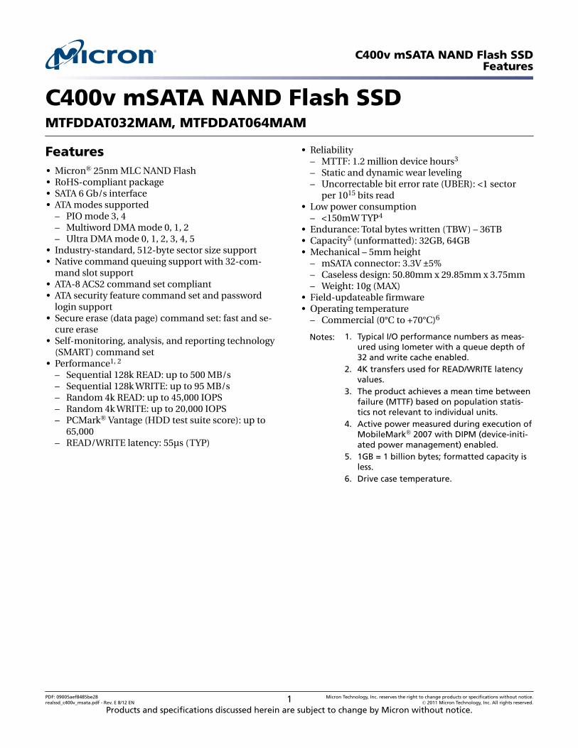
C400v mSATA NAND Flash SSDMTFDDAT032MAM, MTFDDAT064MAM
Features• Micron® 25nm MLC NAND Flash• RoHS-compliant package• SATA 6 Gb/s interface• ATA modes supported
– PIO mode 3, 4– Multiword DMA mode 0, 1, 2– Ultra DMA mode 0, 1, 2, 3, 4, 5
• Industry-standard, 512-byte sector size support• Native command queuing support with 32-com-
mand slot support• ATA-8 ACS2 command set compliant• ATA security feature command set and password
login support• Secure erase (data page) command set: fast and se-
cure erase• Self-monitoring, analysis, and reporting technology
(SMART) command set• Performance1, 2
– Sequential 128k READ: up to 500 MB/s– Sequential 128k WRITE: up to 95 MB/s– Random 4k READ: up to 45,000 IOPS– Random 4k WRITE: up to 20,000 IOPS– PCMark® Vantage (HDD test suite score): up to
65,000– READ/WRITE latency: 55µs (TYP)
• Reliability– MTTF: 1.2 million device hours3
– Static and dynamic wear leveling– Uncorrectable bit error rate (UBER): <1 sector
per 1015 bits read• Low power consumption
– <150mW TYP4
• Endurance: Total bytes written (TBW) – 36TB• Capacity5 (unformatted): 32GB, 64GB• Mechanical – 5mm height
– mSATA connector: 3.3V ±5%– Caseless design: 50.80mm x 29.85mm x 3.75mm– Weight: 10g (MAX)
• Field-updateable firmware• Operating temperature
– Commercial (0°C to +70°C)6
Notes: 1. Typical I/O performance numbers as meas-ured using Iometer with a queue depth of32 and write cache enabled.
2. 4K transfers used for READ/WRITE latencyvalues.
3. The product achieves a mean time betweenfailure (MTTF) based on population statis-tics not relevant to individual units.
4. Active power measured during execution ofMobileMark® 2007 with DIPM (device-initi-ated power management) enabled.
5. 1GB = 1 billion bytes; formatted capacity isless.
6. Drive case temperature.
C400v mSATA NAND Flash SSDFeatures
PDF: 09005aef8485be28realssd_c400v_msata.pdf - Rev. E 8/12 EN 1 Micron Technology, Inc. reserves the right to change products or specifications without notice.
© 2011 Micron Technology, Inc. All rights reserved.
Products and specifications discussed herein are subject to change by Micron without notice.
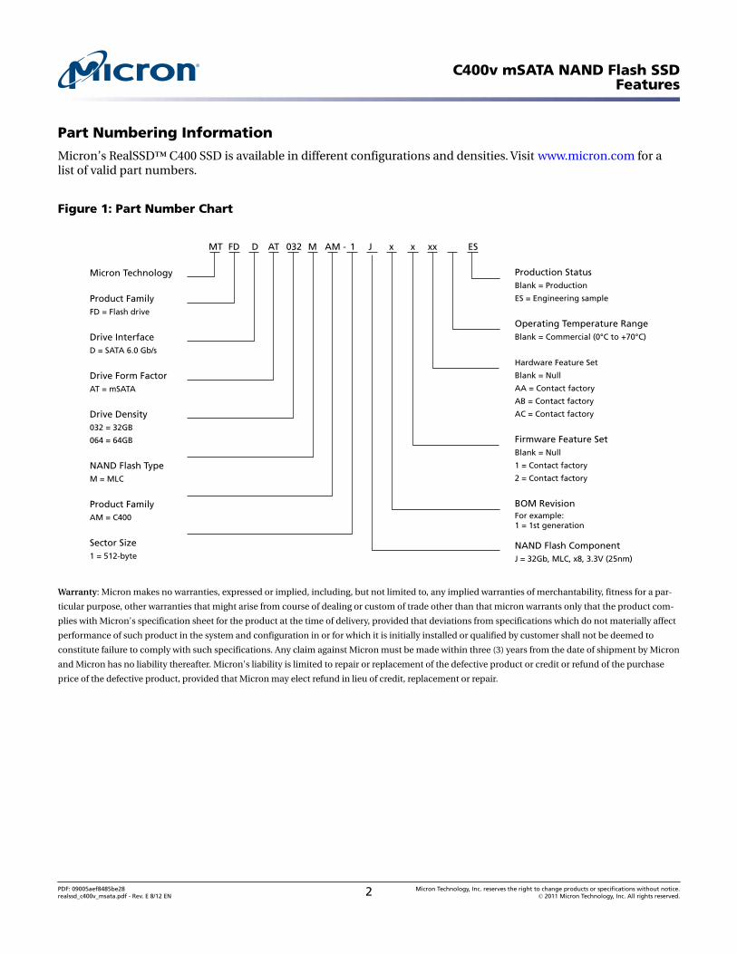
Part Numbering Information
Micron’s RealSSD™ C400 SSD is available in different configurations and densities. Visit www.micron.com for alist of valid part numbers.
Figure 1: Part Number Chart
MT FD D AT 032 M AM - 1 J x ES
Micron Technology
Product FamilyFD = Flash drive
Drive InterfaceD = SATA 6.0 Gb/s
Drive Form FactorAT = mSATA
Drive Density032 = 32GB
064 = 64GB
NAND Flash TypeM = MLC
Product FamilyAM = C400
Sector Size1 = 512-byte
Production StatusBlank = Production
ES = Engineering sample
Operating Temperature RangeBlank = Commercial (0°C to +70°C)
Hardware Feature Set
Blank = Null
AA = Contact factory
AB = Contact factory
AC = Contact factory
Firmware Feature SetBlank = Null
1 = Contact factory
2 = Contact factory
BOM RevisionFor example:1 = 1st generation
NAND Flash ComponentJ = 32Gb, MLC, x8, 3.3V (25nm)
x xx
Warranty: Micron makes no warranties, expressed or implied, including, but not limited to, any implied warranties of merchantability, fitness for a par-
ticular purpose, other warranties that might arise from course of dealing or custom of trade other than that micron warrants only that the product com-
plies with Micron's specification sheet for the product at the time of delivery, provided that deviations from specifications which do not materially affect
performance of such product in the system and configuration in or for which it is initially installed or qualified by customer shall not be deemed to
constitute failure to comply with such specifications. Any claim against Micron must be made within three (3) years from the date of shipment by Micron
and Micron has no liability thereafter. Micron's liability is limited to repair or replacement of the defective product or credit or refund of the purchase
price of the defective product, provided that Micron may elect refund in lieu of credit, replacement or repair.
C400v mSATA NAND Flash SSDFeatures
PDF: 09005aef8485be28realssd_c400v_msata.pdf - Rev. E 8/12 EN 2 Micron Technology, Inc. reserves the right to change products or specifications without notice.
© 2011 Micron Technology, Inc. All rights reserved.
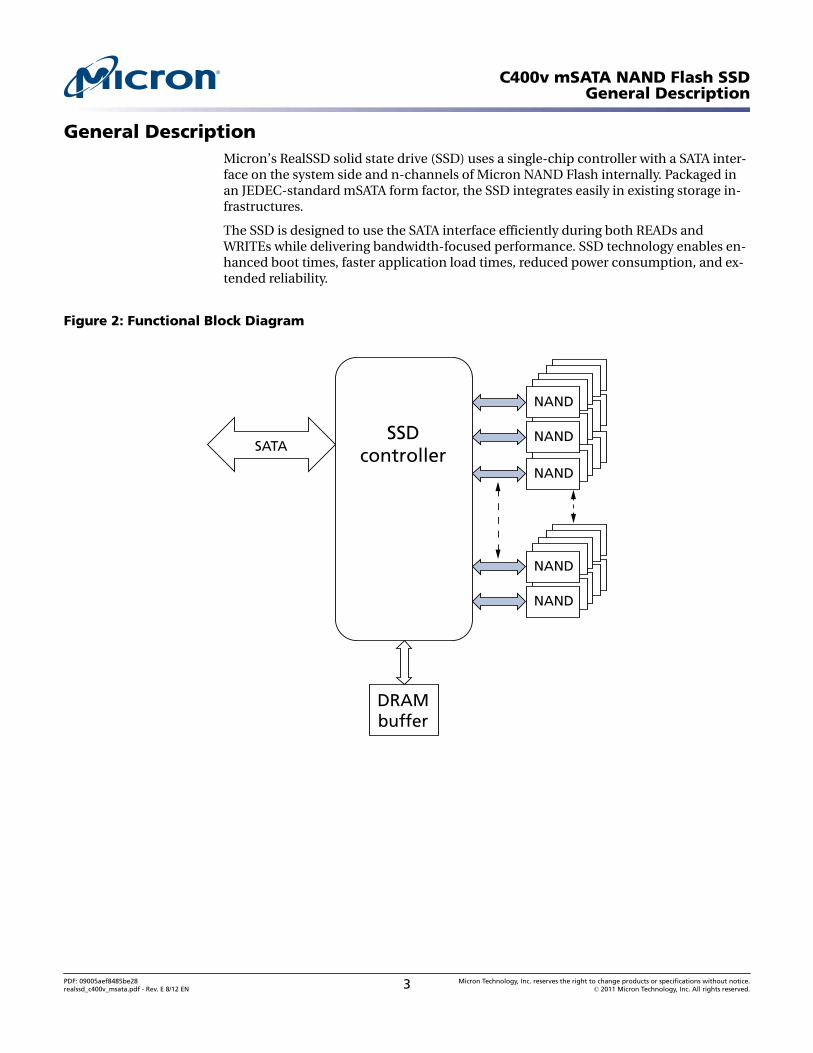
General DescriptionMicron’s RealSSD solid state drive (SSD) uses a single-chip controller with a SATA inter-face on the system side and n-channels of Micron NAND Flash internally. Packaged inan JEDEC-standard mSATA form factor, the SSD integrates easily in existing storage in-frastructures.
The SSD is designed to use the SATA interface efficiently during both READs andWRITEs while delivering bandwidth-focused performance. SSD technology enables en-hanced boot times, faster application load times, reduced power consumption, and ex-tended reliability.
Figure 2: Functional Block Diagram
NAND
SATA
NAND
NAND
NAND
SSDcontroller
DRAMbuffer
NAND
C400v mSATA NAND Flash SSDGeneral Description
PDF: 09005aef8485be28realssd_c400v_msata.pdf - Rev. E 8/12 EN 3 Micron Technology, Inc. reserves the right to change products or specifications without notice.
© 2011 Micron Technology, Inc. All rights reserved.
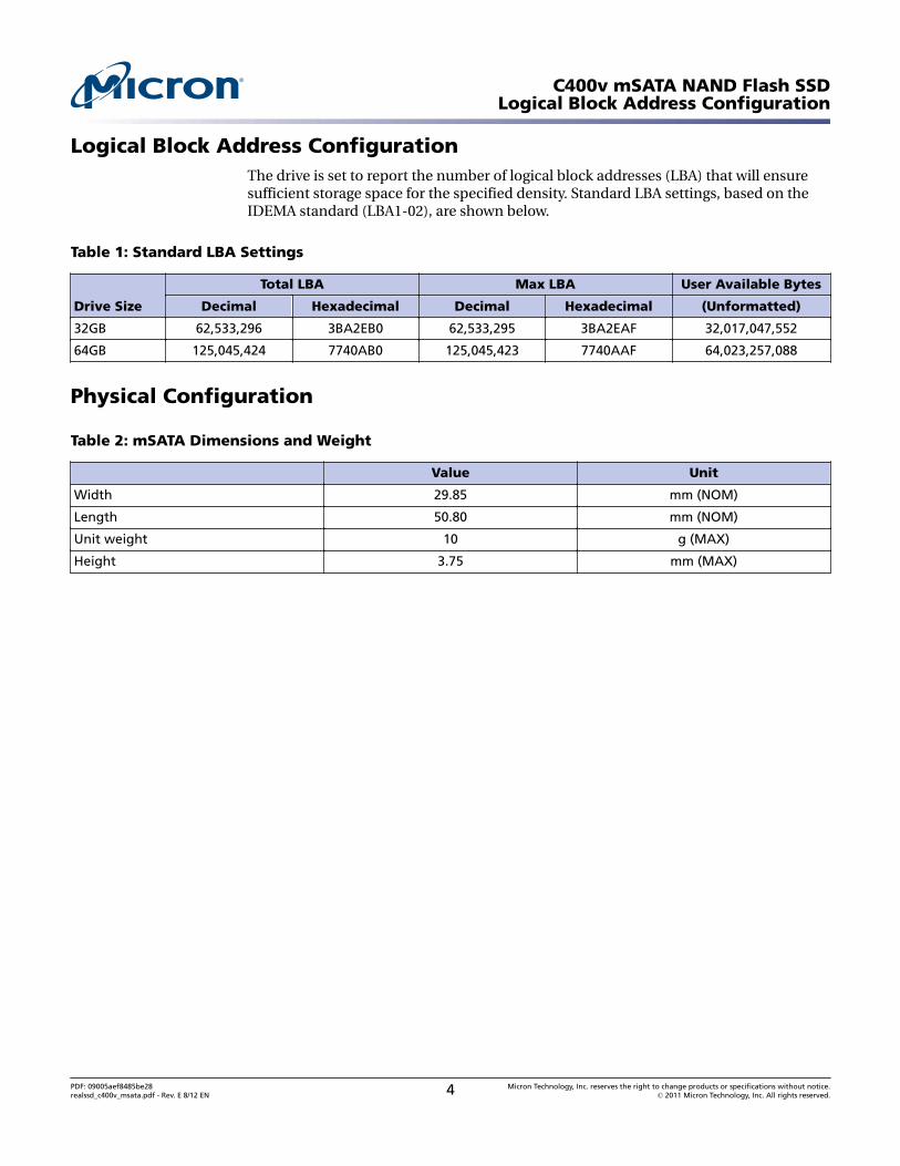
Logical Block Address ConfigurationThe drive is set to report the number of logical block addresses (LBA) that will ensuresufficient storage space for the specified density. Standard LBA settings, based on theIDEMA standard (LBA1-02), are shown below.
Table 1: Standard LBA Settings
Drive Size
Total LBA Max LBA User Available Bytes
Decimal Hexadecimal Decimal Hexadecimal (Unformatted)
32GB 62,533,296 3BA2EB0 62,533,295 3BA2EAF 32,017,047,552
64GB 125,045,424 7740AB0 125,045,423 7740AAF 64,023,257,088
Physical Configuration
Table 2: mSATA Dimensions and Weight
Value Unit
Width 29.85 mm (NOM)
Length 50.80 mm (NOM)
Unit weight 10 g (MAX)
Height 3.75 mm (MAX)
C400v mSATA NAND Flash SSDLogical Block Address Configuration
PDF: 09005aef8485be28realssd_c400v_msata.pdf - Rev. E 8/12 EN 4 Micron Technology, Inc. reserves the right to change products or specifications without notice.
© 2011 Micron Technology, Inc. All rights reserved.
Interface Connectors
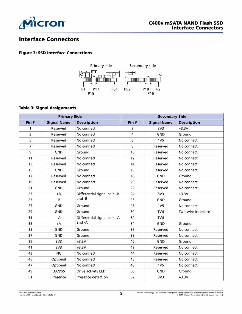
Figure 3: SSD Interface Connections
P1P15
Primary side Secondary side
P17 P51 P52 P18P16
P2
Table 3: Signal Assignments
Primary Side Secondary Side
Pin # Signal Name Description Pin # Signal Name Description
1 Reserved No connect 2 3V3 +3.3V
3 Reserved No connect 4 GND Ground
5 Reserved No connect 6 1V5 No connect
7 Reserved No connect 8 Reserved No connect
9 GND Ground 10 Reserved No connect
11 Reserved No connect 12 Reserved No connect
13 Reserved No connect 14 Reserved No connect
15 GND Ground 16 Reserved No connect
17 Reserved No connect 18 GND Ground
19 Reserved No connect 20 Reserved No connect
21 GND Ground 22 Reserved No connect
23 +B Differential signal pair +Band -B
24 3V3 +3.3V
25 -B 26 GND Ground
27 GND Ground 28 1V5 No connect
29 GND Ground 30 TWI Two-wire interface
31 -A Differential signal pair +Aand -A
32 TWI
33 +A 34 GND Ground
35 GND Ground 36 Reserved No connect
37 GND Ground 38 Reserved No connect
39 3V3 +3.3V 40 GND Ground
41 3V3 +3.3V 42 Reserved No connect
43 NC No connect 44 Reserved No connect
45 Optional No connect 46 Reserved No connect
47 Optional No connect 48 1V5 No connect
49 DA/DSS Drive activity LED 50 GND Ground
51 Presence Presence detection 52 3V3 +3.3V
C400v mSATA NAND Flash SSDInterface Connectors
PDF: 09005aef8485be28realssd_c400v_msata.pdf - Rev. E 8/12 EN 5 Micron Technology, Inc. reserves the right to change products or specifications without notice.
© 2011 Micron Technology, Inc. All rights reserved.
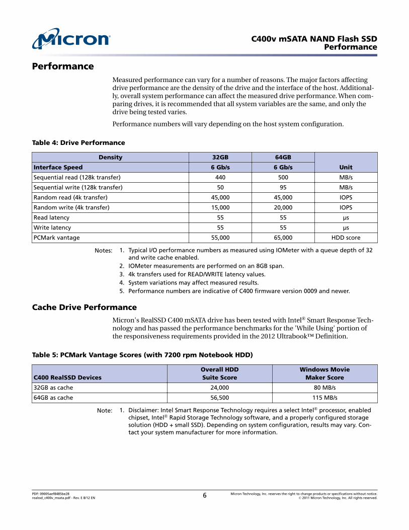
PerformanceMeasured performance can vary for a number of reasons. The major factors affectingdrive performance are the density of the drive and the interface of the host. Additional-ly, overall system performance can affect the measured drive performance. When com-paring drives, it is recommended that all system variables are the same, and only thedrive being tested varies.
Performance numbers will vary depending on the host system configuration.
Table 4: Drive Performance
Density 32GB 64GB
UnitInterface Speed 6 Gb/s 6 Gb/s
Sequential read (128k transfer) 440 500 MB/s
Sequential write (128k transfer) 50 95 MB/s
Random read (4k transfer) 45,000 45,000 IOPS
Random write (4k transfer) 15,000 20,000 IOPS
Read latency 55 55 µs
Write latency 55 55 µs
PCMark vantage 55,000 65,000 HDD score
Notes: 1. Typical I/O performance numbers as measured using IOMeter with a queue depth of 32and write cache enabled.
2. IOMeter measurements are performed on an 8GB span.3. 4k transfers used for READ/WRITE latency values.4. System variations may affect measured results.5. Performance numbers are indicative of C400 firmware version 0009 and newer.
Cache Drive Performance
Micron's RealSSD C400 mSATA drive has been tested with Intel® Smart Response Tech-nology and has passed the performance benchmarks for the 'While Using' portion ofthe responsiveness requirements provided in the 2012 Ultrabook™ Definition.
Table 5: PCMark Vantage Scores (with 7200 rpm Notebook HDD)
C400 RealSSD DevicesOverall HDDSuite Score
Windows MovieMaker Score
32GB as cache 24,000 80 MB/s
64GB as cache 56,500 115 MB/s
Note: 1. Disclaimer: Intel Smart Response Technology requires a select Intel® processor, enabledchipset, Intel® Rapid Storage Technology software, and a properly configured storagesolution (HDD + small SSD). Depending on system configuration, results may vary. Con-tact your system manufacturer for more information.
C400v mSATA NAND Flash SSDPerformance
PDF: 09005aef8485be28realssd_c400v_msata.pdf - Rev. E 8/12 EN 6 Micron Technology, Inc. reserves the right to change products or specifications without notice.
© 2011 Micron Technology, Inc. All rights reserved.
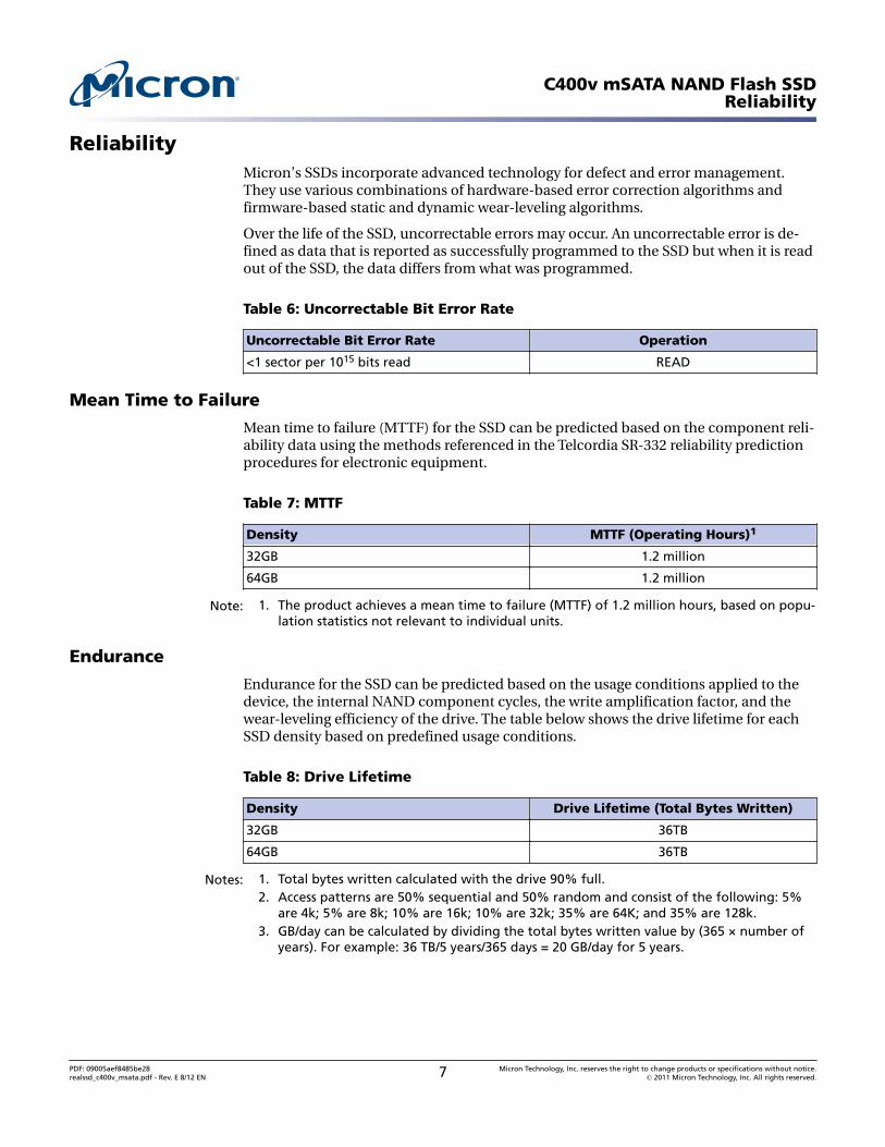
ReliabilityMicron’s SSDs incorporate advanced technology for defect and error management.They use various combinations of hardware-based error correction algorithms andfirmware-based static and dynamic wear-leveling algorithms.
Over the life of the SSD, uncorrectable errors may occur. An uncorrectable error is de-fined as data that is reported as successfully programmed to the SSD but when it is readout of the SSD, the data differs from what was programmed.
Table 6: Uncorrectable Bit Error Rate
Uncorrectable Bit Error Rate Operation
<1 sector per 1015 bits read READ
Mean Time to Failure
Mean time to failure (MTTF) for the SSD can be predicted based on the component reli-ability data using the methods referenced in the Telcordia SR-332 reliability predictionprocedures for electronic equipment.
Table 7: MTTF
Density MTTF (Operating Hours)1
32GB 1.2 million
64GB 1.2 million
Note: 1. The product achieves a mean time to failure (MTTF) of 1.2 million hours, based on popu-lation statistics not relevant to individual units.
Endurance
Endurance for the SSD can be predicted based on the usage conditions applied to thedevice, the internal NAND component cycles, the write amplification factor, and thewear-leveling efficiency of the drive. The table below shows the drive lifetime for eachSSD density based on predefined usage conditions.
Table 8: Drive Lifetime
Density Drive Lifetime (Total Bytes Written)
32GB 36TB
64GB 36TB
Notes: 1. Total bytes written calculated with the drive 90% full.2. Access patterns are 50% sequential and 50% random and consist of the following: 5%
are 4k; 5% are 8k; 10% are 16k; 10% are 32k; 35% are 64K; and 35% are 128k.3. GB/day can be calculated by dividing the total bytes written value by (365 × number of
years). For example: 36 TB/5 years/365 days = 20 GB/day for 5 years.
C400v mSATA NAND Flash SSDReliability
PDF: 09005aef8485be28realssd_c400v_msata.pdf - Rev. E 8/12 EN 7 Micron Technology, Inc. reserves the right to change products or specifications without notice.
© 2011 Micron Technology, Inc. All rights reserved.
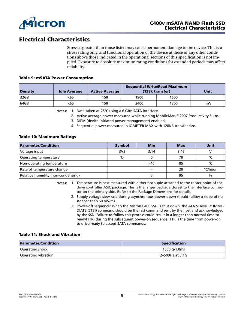
Electrical CharacteristicsStresses greater than those listed may cause permanent damage to the device. This is astress rating only, and functional operation of the device at these or any other condi-tions above those indicated in the operational sections of this specification is not im-plied. Exposure to absolute maximum rating conditions for extended periods may affectreliability.
Table 9: mSATA Power Consumption
Density Idle Average Active AverageSequential Write/Read Maximum
(128k transfer) Unit
32GB <65 150 1900 1600
64GB <65 150 2400 1700 mW
Notes: 1. Data taken at 25°C using a 6 Gb/s SATA interface.2. Active average power measured while running MobileMark® 2007 Productivity Suite.3. DIPM (device-initiated power management) enabled.4. Sequential power measured in IOMETER MAX with 128KB transfer size.
Table 10: Maximum Ratings
Parameter/Condition Symbol Min Max Unit
Voltage input 3V3 3.14 3.46 V
Operating temperature TC 0 70 °C
Non-operating temperature –40 85 °C
Rate of temperature change – 20 °C/hour
Relative humidity (non-condensing) 5 95 %
Notes: 1. Temperature is best measured with a thermocouple attached to the center point of thedrive controller ASIC package. This is the larger package closest to the interface connec-tor on the primary side. Refer to the Package Dimensions for details.
2. Supply voltage slew rate during asynchronous power-down should follow a slope of nosteeper than 60 mV/ms.
3. Power-off sequence: When the Micron C400 SSD is shut down, the ATA STANDBY IMME-DIATE (STBI) command should be the last command sent by the host and acknowledgedby the SSD. Failure to follow this process could result in a longer than normal time-to-ready(TTR) during the subsequent power-on sequence. TTR is the time from power-onto drive ready to accept SATA commands.
Table 11: Shock and Vibration
Parameter/Condition Specification
Operating shock 1500 G/1.0ms
Operating vibration 2–500Hz at 3.1G
C400v mSATA NAND Flash SSDElectrical Characteristics
PDF: 09005aef8485be28realssd_c400v_msata.pdf - Rev. E 8/12 EN 8 Micron Technology, Inc. reserves the right to change products or specifications without notice.
© 2011 Micron Technology, Inc. All rights reserved.
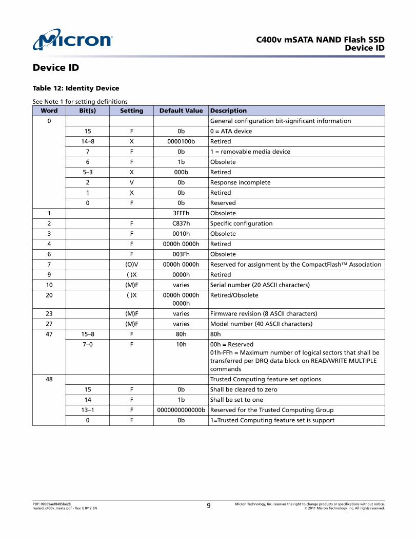
Device ID
Table 12: Identity Device
See Note 1 for setting definitionsWord Bit(s) Setting Default Value Description
0 General configuration bit-significant information
15 F 0b 0 = ATA device
14–8 X 0000100b Retired
7 F 0b 1 = removable media device
6 F 1b Obsolete
5–3 X 000b Retired
2 V 0b Response incomplete
1 X 0b Retired
0 F 0b Reserved
1 3FFFh Obsolete
2 F C837h Specific configuration
3 F 0010h Obsolete
4 F 0000h 0000h Retired
6 F 003Fh Obsolete
7 (O)V 0000h 0000h Reserved for assignment by the CompactFlash™ Association
9 ( )X 0000h Retired
10 (M)F varies Serial number (20 ASCII characters)
20 ( )X 0000h 0000h0000h
Retired/Obsolete
23 (M)F varies Firmware revision (8 ASCII characters)
27 (M)F varies Model number (40 ASCII characters)
47 15–8 F 80h 80h
7–0 F 10h 00h = Reserved01h-FFh = Maximum number of logical sectors that shall betransferred per DRQ data block on READ/WRITE MULTIPLEcommands
48 Trusted Computing feature set options
15 F 0b Shall be cleared to zero
14 F 1b Shall be set to one
13–1 F 0000000000000b Reserved for the Trusted Computing Group
0 F 0b 1=Trusted Computing feature set is support
C400v mSATA NAND Flash SSDDevice ID
PDF: 09005aef8485be28realssd_c400v_msata.pdf - Rev. E 8/12 EN 9 Micron Technology, Inc. reserves the right to change products or specifications without notice.
© 2011 Micron Technology, Inc. All rights reserved.

Table 12: Identity Device (Continued)
See Note 1 for setting definitionsWord Bit(s) Setting Default Value Description
49 Capabilities
15–14 F 00b Reserved for the IDENTIFY PACKET DEVICE command.
13 F 1b 1 = Standby timer values as specified in this standard aresupported
0 = Standby timer values shall be managed by the device
12 F 0b Reserved for the IDENTIFY PACKET DEVICE command.
11 F 1b 1= IORDY supported
0 = IORDY may be supported
10 F 1b 1 = IORDY may be disabled
9 1b 1 = LBA supported
8 F 1b 1 = DMA supported.
7–0 F 00000000b Retired
50 Capabilities
15 F 0b Shall be cleared to zero
14 F 1b Shall be set to one
13–2 F 000000000000b Reserved
1 X 0b Obsolete
0 F 1b Shall be set to one to indicate a vendor specific standby tim-er value minimum.
51 ( )X 0000h 0000h Obsolete
53 15–3 F 0000000000000b Reserved
2 F 1b 1 = the fields reported in word 88 are valid0 = the fields reported in word 88 are not valid
1 F 1b 1 = the fields reported in words (70:64) are valid0 = the fields reported in words (70:64) are not valid
0 X 1b Obsolete
54 ()X 3FFFh 0010h003Fh FC10h
00FBh
Obsolete
59 15 F 0b 1 = The BLOCK ERASE EXT command is supported
14 F 0b 1 = The OVERWRITE EXT command is supported
13 F 0b 1 = The CRYPTO SCRAMBLE EXT command is supported
12 F 0b 1 = The Sanitize feature set is supported
11–9 F 000b Reserved
8 V 1b 1 = Multiple sector setting is valid
7–0 V 00000001b xxh = Current setting for number of logical sectors that shallbe transferred per DRQ data block on READ/WRITE MULTI-PLE commands
60 M(F) Varies by capacity Total number of user addressable logical sectors
C400v mSATA NAND Flash SSDDevice ID
PDF: 09005aef8485be28realssd_c400v_msata.pdf - Rev. E 8/12 EN 10 Micron Technology, Inc. reserves the right to change products or specifications without notice.
© 2011 Micron Technology, Inc. All rights reserved.
Table 12: Identity Device (Continued)
See Note 1 for setting definitionsWord Bit(s) Setting Default Value Description
62 ()X 0000h Obsolete
63 15–11 F 00000b Reserved
10 V 0b 1 = Multiword DMA mode 2 is selected0 = Multiword DMA mode 2 is not selected
9 V 0b 1 = Multiword DMA mode 1 is selected0 = Multiword DMA mode 1 is not selected
8 V 0b 1 = Multiword DMA mode 0 is selected0 = Multiword DMA mode 0 is not selected
7–3 F 0000b Reserved
2 F 1b 1 = Multiword DMA mode 2 and below are supported
1 F 1b 1 = Multiword DMA mode 1 and below are supported
0 F 1b 1 = Multiword DMA mode 0 is supported
64 15–8 F 0 Reserved
7–0 F 03h PIO modes supported
65 F 0078h Minimum Multiword DMA transfer cycle time per wordCycle time in nanoseconds
66 F 0078h Manufacturer's recommended Multiword DMA transfer cy-cle timeCycle time in nanoseconds
67 F 0078h Minimum PIO transfer cycle time without flow controlCycle time in nanoseconds
68 F 0078h Minimum PIO transfer cycle time with IORDY flow controlCycle time in nanoseconds
69 F Additional Supported
15 F 0b 1 = CFast Specification Support
14 F 1b 1 = Deterministic read after Trim is supported
13 F 0b 1 = Long Physical Sector Alignment Error Reporting Controlis supported
12 F 0b 1 = DEVICE CONFIGURATION IDENTIFY DMA and DEVICECONFIGURATION SET DMA are supported
11 F 0b 1 = READ BUFFER DMA is supported
10 F 0b 1 = WRITE BUFFER DMA is supported
9 F 0b 1 = SET MAX PASSWORD DMA and SET MAX UNLOCK DMAare supported
8 F 0b 1 = DOWNLOAD MICROCODE DMA is supported
7 F 0b Reserved for IEEE-1667
6 F 0b 1 = Optional ATA device 28-bit commands supported
5 F 0b 1 = Read zero after Trim is supported
4–0 F 00000b Reserved
70 F 0000h Reserved
C400v mSATA NAND Flash SSDDevice ID
PDF: 09005aef8485be28realssd_c400v_msata.pdf - Rev. E 8/12 EN 11 Micron Technology, Inc. reserves the right to change products or specifications without notice.
© 2011 Micron Technology, Inc. All rights reserved.

Table 12: Identity Device (Continued)
See Note 1 for setting definitionsWord Bit(s) Setting Default Value Description
71 F 0000h 0000h0000h 0000h
Reserved for the IDENTIFY PACKET DEVICE command
75 Queue depth
15–5 F 00000000000b Reserved
4–0 F 11111b Maximum queue depth - 1
76 Serial ATA Capabilities
15–13 F 000b Reserved
12 F 1b Supports Native Command Queuing priority information
11 F 0b Supports Unload while NCQ commands outstanding
10 F 1b Supports Phy event counters
9 F 1b Supports receipt of host initiated interface power manage-ment requestsNOTE: HIPM is disabled (bit 9 = 0) for firmware versions000G and newer
8 F 1b Supports native Command Queueing
7–4 F 0000b Reserved for future Serial ATA signaling speed grades
3 F 1b 1 = Supports Serial ATA Gen-3 speed (6.0 Gb/s)
2 F 1b 1 = Supports Serial ATA Gen-2 speed (3.0 Gb/s)
1 F 1b 1 = Supports Serial ATA Gen-1 speed (1.5 Gb/s)
0 F 0b Reserved (set to 0)
77 Serial ATA Additional capabilities
15–6 F 0000000000b Reserved for future Serial ATA definition
5 F 0b Supports NCQ Queue Management Command
4 F 0b Supports NCQ Streaming
3–1 V 010b Coded value indicating current negotiated Serial ATA signalspeed
0 F 0b Shall be cleared to zero
78 Serial ATA features Supported
15–7 F 000000000b Reserved
6 F 1b 1 = supports software settings preservation
5 F 0b Reserved
4 F 0b 1 = supports in-order data delivery
3 F 1b 1 = supports dev initiate interface power management
2 F 1b 1 = supports DMA Setup Auto-Activate optimization
1 F 0b 1 = supports non-zero buffer offsets in DMA Setup FIS
0 F 0b Reserved (set to 0)
C400v mSATA NAND Flash SSDDevice ID
PDF: 09005aef8485be28realssd_c400v_msata.pdf - Rev. E 8/12 EN 12 Micron Technology, Inc. reserves the right to change products or specifications without notice.
© 2011 Micron Technology, Inc. All rights reserved.

Table 12: Identity Device (Continued)
See Note 1 for setting definitionsWord Bit(s) Setting Default Value Description
79 Serial ATA features Enabled
15–7 V 000000000b Reserved
6 V 1b 1 = software settings preservation enabled
5 V 0b 1 = Asynchronous notification enabled
4 V 0b 1 = in-order data delivery enabled
3 V 0b 1 = device initiating interface power management enabled
2 V 0b 1 = DMA Setup Auto-Activate optimization enabled
1 V 0b 1 = non-zero buffer offsets in DMA Setup FIS enabled
0 V 0b Reserved (set to 0)
80 Major revision number
15–10 F 000000b Reserved
9 F 1b 1 = supports ATA8-ACS2
8 F 1b 1 = supports ATA8-ACS
7 F 1b 1 = supports ATA/ATAPI-7
6 F 1b 1 = supports ATA/ATAPI-6
5 F 1b 1 = supports ATA/ATAPI-5
4 F 1b 1 = supports ATA/ATAPI-4
3 F 1b Obsolete
2 S 0b Obsolete
1 S 0b Obsolete
0 F 0b Reserved
81 F 0028h Minor revision number
0028h = ATA8-ACS version 6
C400v mSATA NAND Flash SSDDevice ID
PDF: 09005aef8485be28realssd_c400v_msata.pdf - Rev. E 8/12 EN 13 Micron Technology, Inc. reserves the right to change products or specifications without notice.
© 2011 Micron Technology, Inc. All rights reserved.
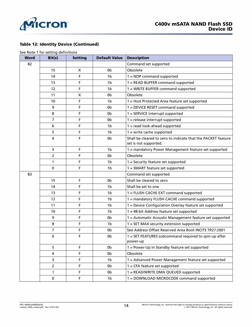
Table 12: Identity Device (Continued)
See Note 1 for setting definitionsWord Bit(s) Setting Default Value Description
82 Command set supported
15 X 0b Obsolete
14 F 1b 1 = NOP command supported
13 F 1b 1 = READ BUFFER command supported
12 F 1b 1 = WRITE BUFFER command supported
11 X 0b Obsolete
10 F 1b 1 = Host Protected Area feature set supported
9 F 0b 1 = DEVICE RESET command supported
8 F 0b 1 = SERVICE interrupt supported
7 F 0b 1 = release interrupt supported
6 F 1b 1 = read look-ahead supported
5 F 1b 1 = write cache supported
4 F 0b Shall be cleared to zero to indicate that the PACKET featureset is not supported.
3 F 1b 1 = mandatory Power Management feature set supported
2 F 0b Obsolete
1 F 1b 1 = Security feature set supported
0 F 1b 1 = SMART feature set supported
83 Command set supported
15 F 0b Shall be cleared to zero
14 F 1b Shall be set to one
13 F 1b 1 = FLUSH CACHE EXT command supported
12 F 1b 1 = mandatory FLUSH CACHE command supported
11 F 1b 1 = Device Configuration Overlay feature set supported
10 F 1b 1 = 48-bit Address feature set supported
9 F 0b 1 = Automatic Acoustic Management feature set supported
8 F 1b 1 = SET MAX security extension supported
7 F 0b See Address Offset Reserved Area Boot INCITS TR27:2001
6 F 0b 1 = SET FEATURES subcommand required to spin-up afterpower-up
5 F 0b 1 = Power-Up In Standby feature set supported
4 F 0b Obsolete
3 F 1b 1 = Advanced Power Management feature set supported
2 F 0b 1 = CFA feature set supported
1 F 0b 1 = READ/WRITE DMA QUEUED supported
0 F 1b 1 = DOWNLOAD MICROCODE command supported
C400v mSATA NAND Flash SSDDevice ID
PDF: 09005aef8485be28realssd_c400v_msata.pdf - Rev. E 8/12 EN 14 Micron Technology, Inc. reserves the right to change products or specifications without notice.
© 2011 Micron Technology, Inc. All rights reserved.
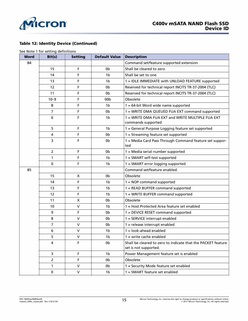
Table 12: Identity Device (Continued)
See Note 1 for setting definitionsWord Bit(s) Setting Default Value Description
84 Command set/feature supported extension
15 F 0b Shall be cleared to zero
14 F 1b Shall be set to one
13 F 1b 1 = IDLE IMMEDIATE with UNLOAD FEATURE supported
12 F 0b Reserved for technical report INCITS TR-37-2004 (TLC)
11 F 0b Reserved for technical report INCITS TR-37-2004 (TLC)
10–9 F 00b Obsolete
8 F 1b 1 = 64-bit Word wide name supported
7 F 0b 1 = WRITE DMA QUEUED FUA EXT command supported
6 F 1b 1 = WRITE DMA FUA EXT and WRITE MULTIPLE FUA EXTcommands supported
5 F 1b 1 = General Purpose Logging feature set supported
4 F 0b 1 = Streaming feature set supported
3 F 0b 1 = Media Card Pass Through Command feature set suppor-ted
2 F 0b 1 = Media serial number supported
1 F 1b 1 = SMART self-test supported
0 F 1b 1 = SMART error logging supported
85 Command set/feature enabled.
15 X 0b Obsolete
14 F 1b 1 = NOP command supported
13 F 1b 1 = READ BUFFER command supported
12 F 1b 1 = WRITE BUFFER command supported
11 X 0b Obsolete
10 V 1b 1 = Host Protected Area feature set enabled
9 F 0b 1 = DEVICE RESET command supported
8 V 0b 1 = SERVICE interrupt enabled
7 V 0b 1 = release interrupt enabled
6 V 1b 1 = look-ahead enabled
5 V 1b 1 = write cache enabled
4 F 0b Shall be cleared to zero to indicate that the PACKET featureset is not supported.
3 F 1b Power Management feature set is enabled
2 F 0b Obsolete
1 V 0b 1 = Security Mode feature set enabled
0 V 1b 1 = SMART feature set enabled
C400v mSATA NAND Flash SSDDevice ID
PDF: 09005aef8485be28realssd_c400v_msata.pdf - Rev. E 8/12 EN 15 Micron Technology, Inc. reserves the right to change products or specifications without notice.
© 2011 Micron Technology, Inc. All rights reserved.
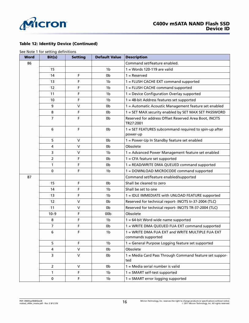
Table 12: Identity Device (Continued)
See Note 1 for setting definitionsWord Bit(s) Setting Default Value Description
86 Command set/feature enabled.
15 1b 1 = Words 120-119 are valid
14 F 0b 1 = Reserved
13 F 1b 1 = FLUSH CACHE EXT command supported
12 F 1b 1 = FLUSH CACHE command supported
11 F 1b 1 = Device Configuration Overlay supported
10 F 1b 1 = 48-bit Address features set supported
9 V 0b 1 = Automatic Acoustic Management feature set enabled
8 F 0b 1 = SET MAX security enabled by SET MAX SET PASSWORD
7 F 0b Reserved for address Offset Reserved Area Boot, INCITSTR27:2001
6 F 0b 1 = SET FEATURES subcommand required to spin-up afterpower-up
5 V 0b 1 = Power-Up In Standby feature set enabled
4 V 0b Obsolete
3 V 1b 1 = Advanced Power Management feature set enabled
2 F 0b 1 = CFA feature set supported
1 F 0b 1 = READ/WRITE DMA QUEUED command supported
0 F 1b 1 = DOWNLOAD MICROCODE command supported
87 Command set/feature enabled/supported
15 F 0b Shall be cleared to zero
14 F 1b Shall be set to one
13 F 1b 1 = IDLE IMMEDIATE with UNLOAD FEATURE supported
12 V 0b Reserved for technical report- INCITS tr-37-2004 (TLC)
11 V 0b Reserved for technical report- INCITS TR-37-2004 (TLC)
10–9 F 00b Obsolete
8 F 1b 1 = 64-bit Word wide name supported
7 F 0b 1 = WRITE DMA QUEUED FUA EXT command supported
6 F 1b 1 = WRITE DMA FUA EXT and WRITE MULTIPLE FUA EXTcommands supported
5 F 1b 1 = General Purpose Logging feature set supported
4 V 0b Obsolete
3 V 0b 1 = Media Card Pass Through Command feature set suppor-ted
2 V 0b 1 = Media serial number is valid
1 F 1b 1 = SMART self-test supported
0 F 1b 1 = SMART error logging supported
C400v mSATA NAND Flash SSDDevice ID
PDF: 09005aef8485be28realssd_c400v_msata.pdf - Rev. E 8/12 EN 16 Micron Technology, Inc. reserves the right to change products or specifications without notice.
© 2011 Micron Technology, Inc. All rights reserved.
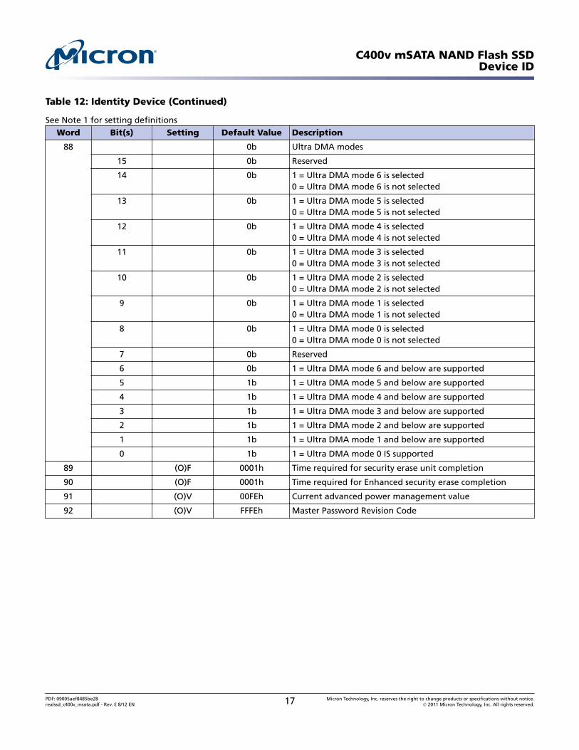
Table 12: Identity Device (Continued)
See Note 1 for setting definitionsWord Bit(s) Setting Default Value Description
88 0b Ultra DMA modes
15 0b Reserved
14 0b 1 = Ultra DMA mode 6 is selected0 = Ultra DMA mode 6 is not selected
13 0b 1 = Ultra DMA mode 5 is selected0 = Ultra DMA mode 5 is not selected
12 0b 1 = Ultra DMA mode 4 is selected0 = Ultra DMA mode 4 is not selected
11 0b 1 = Ultra DMA mode 3 is selected0 = Ultra DMA mode 3 is not selected
10 0b 1 = Ultra DMA mode 2 is selected0 = Ultra DMA mode 2 is not selected
9 0b 1 = Ultra DMA mode 1 is selected0 = Ultra DMA mode 1 is not selected
8 0b 1 = Ultra DMA mode 0 is selected0 = Ultra DMA mode 0 is not selected
7 0b Reserved
6 0b 1 = Ultra DMA mode 6 and below are supported
5 1b 1 = Ultra DMA mode 5 and below are supported
4 1b 1 = Ultra DMA mode 4 and below are supported
3 1b 1 = Ultra DMA mode 3 and below are supported
2 1b 1 = Ultra DMA mode 2 and below are supported
1 1b 1 = Ultra DMA mode 1 and below are supported
0 1b 1 = Ultra DMA mode 0 IS supported
89 (O)F 0001h Time required for security erase unit completion
90 (O)F 0001h Time required for Enhanced security erase completion
91 (O)V 00FEh Current advanced power management value
92 (O)V FFFEh Master Password Revision Code
C400v mSATA NAND Flash SSDDevice ID
PDF: 09005aef8485be28realssd_c400v_msata.pdf - Rev. E 8/12 EN 17 Micron Technology, Inc. reserves the right to change products or specifications without notice.
© 2011 Micron Technology, Inc. All rights reserved.
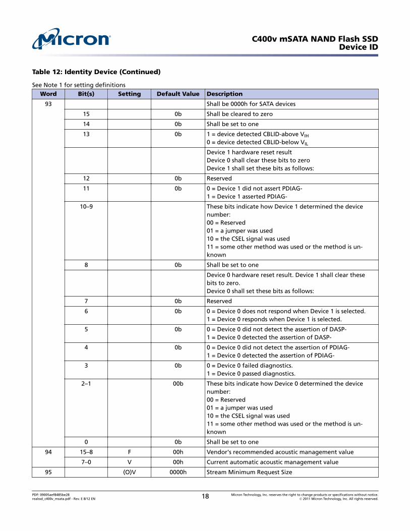
Table 12: Identity Device (Continued)
See Note 1 for setting definitionsWord Bit(s) Setting Default Value Description
93 Shall be 0000h for SATA devices
15 0b Shall be cleared to zero
14 0b Shall be set to one
13 0b 1 = device detected CBLID-above VIH
0 = device detected CBLID-below VIL
Device 1 hardware reset resultDevice 0 shall clear these bits to zeroDevice 1 shall set these bits as follows:
12 0b Reserved
11 0b 0 = Device 1 did not assert PDIAG-1 = Device 1 asserted PDIAG-
10–9 These bits indicate how Device 1 determined the devicenumber:00 = Reserved01 = a jumper was used10 = the CSEL signal was used11 = some other method was used or the method is un-known
8 0b Shall be set to one
Device 0 hardware reset result. Device 1 shall clear thesebits to zero.Device 0 shall set these bits as follows:
7 0b Reserved
6 0b 0 = Device 0 does not respond when Device 1 is selected.1 = Device 0 responds when Device 1 is selected.
5 0b 0 = Device 0 did not detect the assertion of DASP-1 = Device 0 detected the assertion of DASP-
4 0b 0 = Device 0 did not detect the assertion of PDIAG-1 = Device 0 detected the assertion of PDIAG-
3 0b 0 = Device 0 failed diagnostics.1 = Device 0 passed diagnostics.
2–1 00b These bits indicate how Device 0 determined the devicenumber:00 = Reserved01 = a jumper was used10 = the CSEL signal was used11 = some other method was used or the method is un-known
0 0b Shall be set to one
94 15–8 F 00h Vendor's recommended acoustic management value
7–0 V 00h Current automatic acoustic management value
95 (O)V 0000h Stream Minimum Request Size
C400v mSATA NAND Flash SSDDevice ID
PDF: 09005aef8485be28realssd_c400v_msata.pdf - Rev. E 8/12 EN 18 Micron Technology, Inc. reserves the right to change products or specifications without notice.
© 2011 Micron Technology, Inc. All rights reserved.

Table 12: Identity Device (Continued)
See Note 1 for setting definitionsWord Bit(s) Setting Default Value Description
96 (O)V 0000h Streaming Transfer Time - DMA
97 (O)V 0000h Streaming Access Latency - DMA and PIO
98 (O)F 0000h 0000h Streaming Performance Granularity(98-99)
100 V Varies by capacity Maximum user LBA for 48-bit Address feature set
104 (O)V 0000h Streaming Transfer Time - PIO
105 ( )F 0008h Maximum number of 512-byte blocks of LBA Range Entriesper DATA SET MANAGEMENT command
106 Physical sector size / Logical Sector Size
15 F 0b Shall be cleared to zero
14 F 1b Shall be set to one
13 F 0b 1 = Device has multiple logical sectors per physical sector
12 F 0b 1 = Device Logical Sector Longer than 256 Words
11–4 F 00000000b Reserved
3–0 F 0000b 2^x logical sectors per physical sector
107 (O)F 0000h Inter-seek delay for ISO-7779 acoustic testing in microsec-onds
108 15–12 F 0101b NAA (3-0)
11–0 000000001010b IEEE OUI (23-12)
109 15–4 F 000001110101b IEEE OUI (11-0)
3–0 Varies Unique ID (35-32)
110 (M)F Varies 5-0 Unique ID (31-16)
111 (M)F Varies Unique ID (15-0)
112 (O)F 0000h 0000h0000h 0000h
Reserved for 128 bit world wide name extension to 128 bits
116 (O)V 0000h Reserved for INCITS TR-37-2004
117 (O)F 0000h 0000h Words per Logical Sector
C400v mSATA NAND Flash SSDDevice ID
PDF: 09005aef8485be28realssd_c400v_msata.pdf - Rev. E 8/12 EN 19 Micron Technology, Inc. reserves the right to change products or specifications without notice.
© 2011 Micron Technology, Inc. All rights reserved.
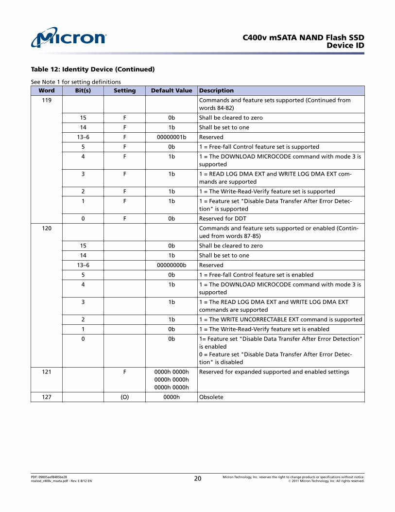
Table 12: Identity Device (Continued)
See Note 1 for setting definitionsWord Bit(s) Setting Default Value Description
119 Commands and feature sets supported (Continued fromwords 84-82)
15 F 0b Shall be cleared to zero
14 F 1b Shall be set to one
13–6 F 00000001b Reserved
5 F 0b 1 = Free-fall Control feature set is supported
4 F 1b 1 = The DOWNLOAD MICROCODE command with mode 3 issupported
3 F 1b 1 = READ LOG DMA EXT and WRITE LOG DMA EXT com-mands are supported
2 F 1b 1 = The Write-Read-Verify feature set is supported
1 F 1b 1 = Feature set "Disable Data Transfer After Error Detec-tion" is supported
0 F 0b Reserved for DDT
120 Commands and feature sets supported or enabled (Contin-ued from words 87-85)
15 0b Shall be cleared to zero
14 1b Shall be set to one
13–6 00000000b Reserved
5 0b 1 = Free-fall Control feature set is enabled
4 1b 1 = The DOWNLOAD MICROCODE command with mode 3 issupported
3 1b 1 = The READ LOG DMA EXT and WRITE LOG DMA EXTcommands are supported
2 1b 1 = The WRITE UNCORRECTABLE EXT command is supported
1 0b 1 = The Write-Read-Verify feature set is enabled
0 0b 1= Feature set "Disable Data Transfer After Error Detection"is enabled0 = Feature set "Disable Data Transfer After Error Detec-tion" is disabled
121 F 0000h 0000h0000h 0000h0000h 0000h
Reserved for expanded supported and enabled settings
127 (O) 0000h Obsolete
C400v mSATA NAND Flash SSDDevice ID
PDF: 09005aef8485be28realssd_c400v_msata.pdf - Rev. E 8/12 EN 20 Micron Technology, Inc. reserves the right to change products or specifications without notice.
© 2011 Micron Technology, Inc. All rights reserved.

Table 12: Identity Device (Continued)
See Note 1 for setting definitionsWord Bit(s) Setting Default Value Description
128 Security status
15–9 F 0000000b Reserved
8 V 0b Security level 0 = High, 1 = Maximum
7–6 F 00b Reserved
5 F 1b 1 = Enhanced security erase supported
4 V 0b 1 = Security count expired
3 V 0b 1 = Security frozen
2 V 0b 1 = Security locked
1 V 0b 1 = Security enabled
0 F 1b 1 = Security supported
129 ( )X Vendor specificdata
Vendor specific
160 CFA power mode 1
15 F 0b Word 160 supported
14 F 0b Reserved
13 F 0b CFA power mode 1 is required for one or more commandsimplemented by the device
12 V 0b CFA power mode 1 disabled
11–0 F 000000000000b Maximum current in ma
161 X 0000h 0000h0000h 0000h0000h 0000h
0000h
Reserved for assignment by the CompactFlash Association
168 15–4 F 000h Reserved
3-0 F 5h Device Nominal Form Factor
169 DATA SET MANAGEMENT command support
15–1 F 000000000000000b
Reserved
0 F 1b 1 = the Trim bit in the DATA SET MANAGEMENT commandis supported
170 F 0000h 0000h0000h 0000h
Additional Product Identifier
174 F 0000h 0000h Reserved
176 (O)V Varies Current media serial number (60 ASCII characters)
C400v mSATA NAND Flash SSDDevice ID
PDF: 09005aef8485be28realssd_c400v_msata.pdf - Rev. E 8/12 EN 21 Micron Technology, Inc. reserves the right to change products or specifications without notice.
© 2011 Micron Technology, Inc. All rights reserved.
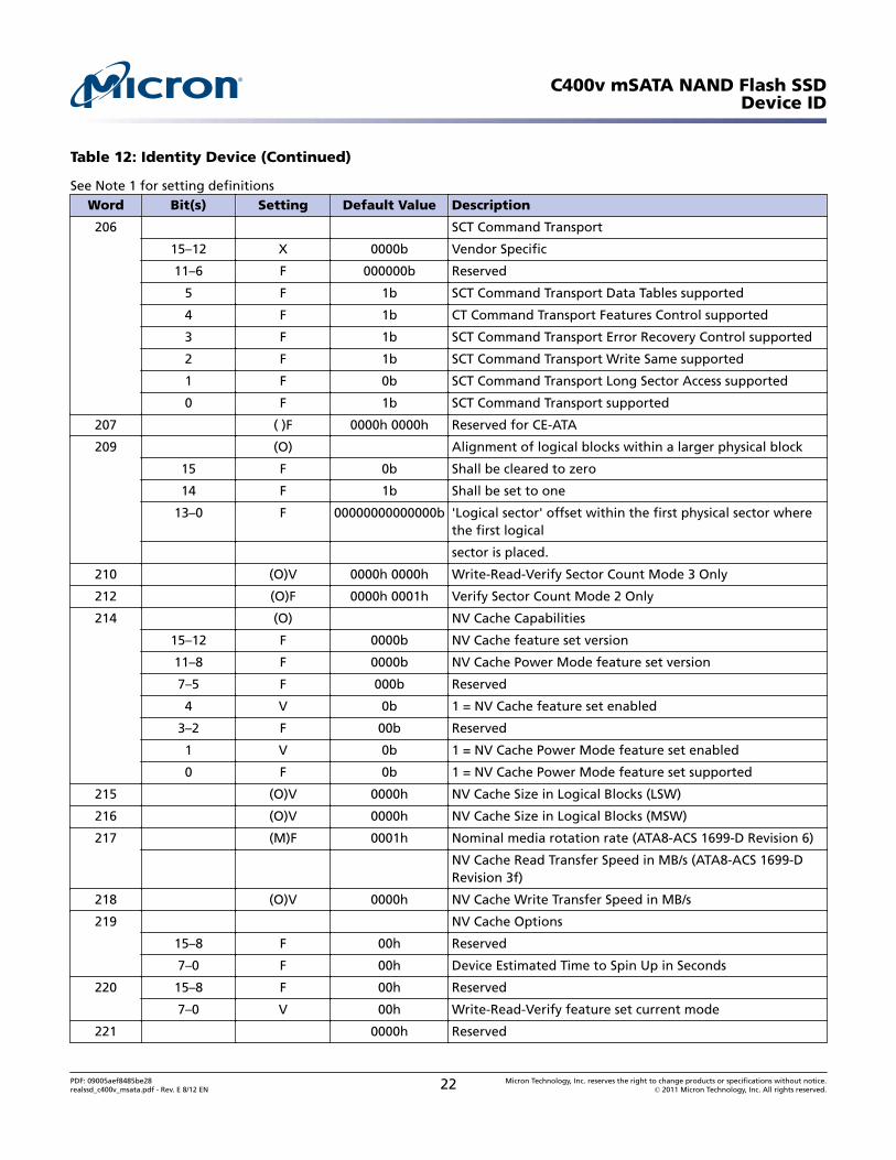
Table 12: Identity Device (Continued)
See Note 1 for setting definitionsWord Bit(s) Setting Default Value Description
206 SCT Command Transport
15–12 X 0000b Vendor Specific
11–6 F 000000b Reserved
5 F 1b SCT Command Transport Data Tables supported
4 F 1b CT Command Transport Features Control supported
3 F 1b SCT Command Transport Error Recovery Control supported
2 F 1b SCT Command Transport Write Same supported
1 F 0b SCT Command Transport Long Sector Access supported
0 F 1b SCT Command Transport supported
207 ( )F 0000h 0000h Reserved for CE-ATA
209 (O) Alignment of logical blocks within a larger physical block
15 F 0b Shall be cleared to zero
14 F 1b Shall be set to one
13–0 F 00000000000000b 'Logical sector' offset within the first physical sector wherethe first logical
sector is placed.
210 (O)V 0000h 0000h Write-Read-Verify Sector Count Mode 3 Only
212 (O)F 0000h 0001h Verify Sector Count Mode 2 Only
214 (O) NV Cache Capabilities
15–12 F 0000b NV Cache feature set version
11–8 F 0000b NV Cache Power Mode feature set version
7–5 F 000b Reserved
4 V 0b 1 = NV Cache feature set enabled
3–2 F 00b Reserved
1 V 0b 1 = NV Cache Power Mode feature set enabled
0 F 0b 1 = NV Cache Power Mode feature set supported
215 (O)V 0000h NV Cache Size in Logical Blocks (LSW)
216 (O)V 0000h NV Cache Size in Logical Blocks (MSW)
217 (M)F 0001h Nominal media rotation rate (ATA8-ACS 1699-D Revision 6)
NV Cache Read Transfer Speed in MB/s (ATA8-ACS 1699-DRevision 3f)
218 (O)V 0000h NV Cache Write Transfer Speed in MB/s
219 NV Cache Options
15–8 F 00h Reserved
7–0 F 00h Device Estimated Time to Spin Up in Seconds
220 15–8 F 00h Reserved
7–0 V 00h Write-Read-Verify feature set current mode
221 0000h Reserved
C400v mSATA NAND Flash SSDDevice ID
PDF: 09005aef8485be28realssd_c400v_msata.pdf - Rev. E 8/12 EN 22 Micron Technology, Inc. reserves the right to change products or specifications without notice.
© 2011 Micron Technology, Inc. All rights reserved.
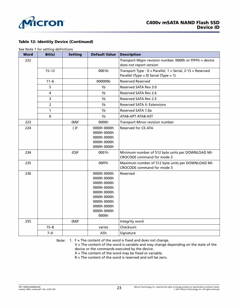
Table 12: Identity Device (Continued)
See Note 1 for setting definitionsWord Bit(s) Setting Default Value Description
222 Transport Major revision number. 0000h or FFFFh = devicedoes not report version
15–12 0001b Transport Type - 0 = Parallel, 1 = Serial, 2-15 = ReservedParallel (Type = 0) Serial (Type = 1)
11–6 000000b Reserved Reserved
5 1b Reserved SATA Rev 3.0
4 1b Reserved SATA Rev 2.6
3 1b Reserved SATA Rev 2.5
2 1b Reserved SATA II: Extensions
1 1b Reserved SATA 1.0a
0 1b ATA8-APT ATA8-AST
223 (M)F 0000h Transport Minor revision number
224 ( )F 0000h 0000h0000h 0000h0000h 0000h0000h 0000h0000h 0000h
Reserved for CE-ATA
234 (O)F 0001h Minimum number of 512 byte units per DOWNLOAD MI-CROCODE command for mode 3
235 00FFh Maximum number of 512 byte units per DOWNLOAD MI-CROCODE command for mode 3
236 0000h 0000h0000h 0000h0000h 0000h0000h 0000h0000h 0000h0000h 0000h0000h 0000h0000h 0000h0000h 0000h
0000h
Reserved
255 (M)F Integrity word
15–8 varies Checksum
7–0 A5h Signature
Note: 1. F = The content of the word is fixed and does not change.V = The content of the word is variable and may change depending on the state of thedevice or the commands executed by the device.X = The content of the word may be fixed or variable.R = The content of the word is reserved and will be zero.
C400v mSATA NAND Flash SSDDevice ID
PDF: 09005aef8485be28realssd_c400v_msata.pdf - Rev. E 8/12 EN 23 Micron Technology, Inc. reserves the right to change products or specifications without notice.
© 2011 Micron Technology, Inc. All rights reserved.
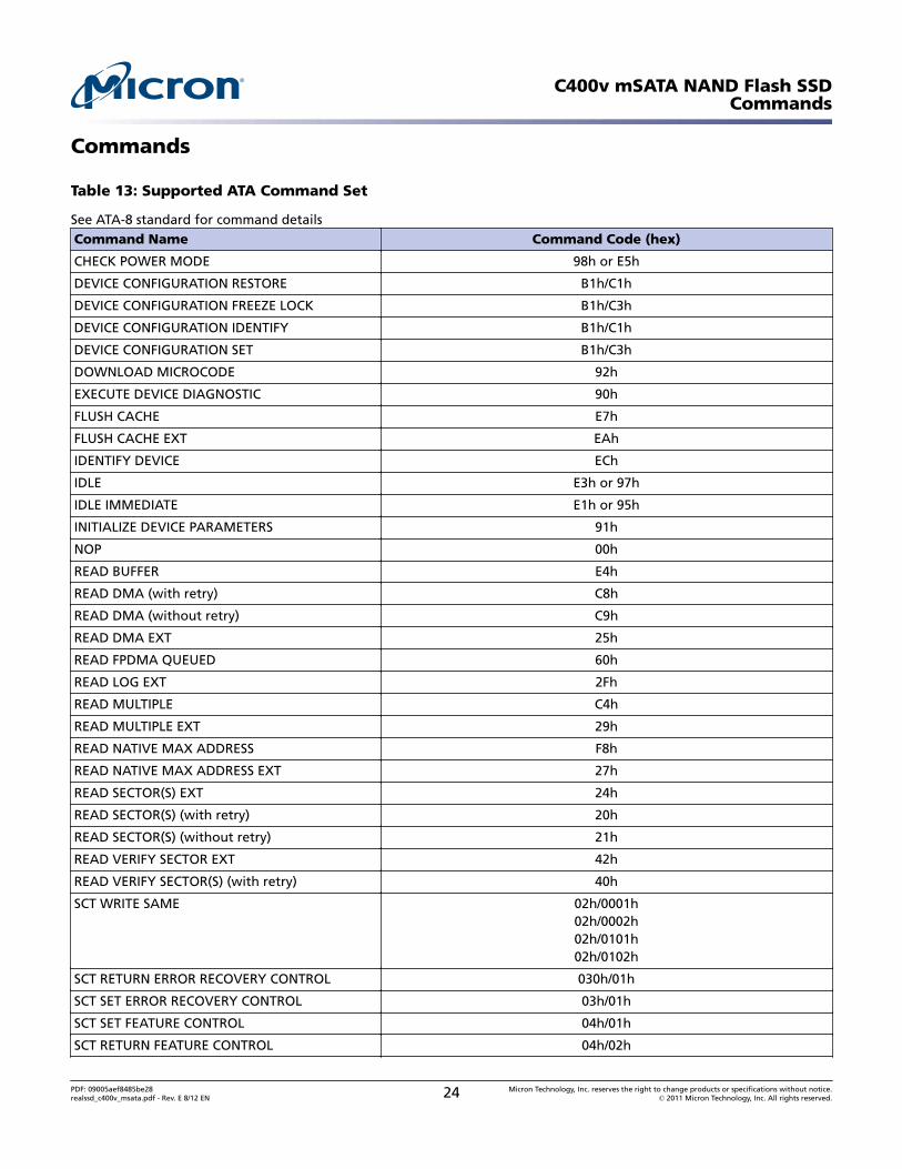
Commands
Table 13: Supported ATA Command Set
See ATA-8 standard for command detailsCommand Name Command Code (hex)
CHECK POWER MODE 98h or E5h
DEVICE CONFIGURATION RESTORE B1h/C1h
DEVICE CONFIGURATION FREEZE LOCK B1h/C3h
DEVICE CONFIGURATION IDENTIFY B1h/C1h
DEVICE CONFIGURATION SET B1h/C3h
DOWNLOAD MICROCODE 92h
EXECUTE DEVICE DIAGNOSTIC 90h
FLUSH CACHE E7h
FLUSH CACHE EXT EAh
IDENTIFY DEVICE ECh
IDLE E3h or 97h
IDLE IMMEDIATE E1h or 95h
INITIALIZE DEVICE PARAMETERS 91h
NOP 00h
READ BUFFER E4h
READ DMA (with retry) C8h
READ DMA (without retry) C9h
READ DMA EXT 25h
READ FPDMA QUEUED 60h
READ LOG EXT 2Fh
READ MULTIPLE C4h
READ MULTIPLE EXT 29h
READ NATIVE MAX ADDRESS F8h
READ NATIVE MAX ADDRESS EXT 27h
READ SECTOR(S) EXT 24h
READ SECTOR(S) (with retry) 20h
READ SECTOR(S) (without retry) 21h
READ VERIFY SECTOR EXT 42h
READ VERIFY SECTOR(S) (with retry) 40h
SCT WRITE SAME 02h/0001h02h/0002h02h/0101h02h/0102h
SCT RETURN ERROR RECOVERY CONTROL 030h/01h
SCT SET ERROR RECOVERY CONTROL 03h/01h
SCT SET FEATURE CONTROL 04h/01h
SCT RETURN FEATURE CONTROL 04h/02h
C400v mSATA NAND Flash SSDCommands
PDF: 09005aef8485be28realssd_c400v_msata.pdf - Rev. E 8/12 EN 24 Micron Technology, Inc. reserves the right to change products or specifications without notice.
© 2011 Micron Technology, Inc. All rights reserved.
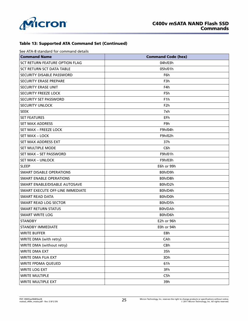
Table 13: Supported ATA Command Set (Continued)
See ATA-8 standard for command detailsCommand Name Command Code (hex)
SCT RETURN FEATURE OPTION FLAG 04h/03h
SCT RETURN SCT DATA TABLE 05h/01h
SECURITY DISABLE PASSWORD F6h
SECURITY ERASE PREPARE F3h
SECURITY ERASE UNIT F4h
SECURITY FREEZE LOCK F5h
SECURITY SET PASSWORD F1h
SECURITY UNLOCK F2h
SEEK 7xh
SET FEATURES EFh
SET MAX ADDRESS F9h
SET MAX – FREEZE LOCK F9h/04h
SET MAX – LOCK F9h/02h
SET MAX ADDRESS EXT 37h
SET MULTIPLE MODE C6h
SET MAX – SET PASSWORD F9h/01h
SET MAX – UNLOCK F9h/03h
SLEEP E6h or 99h
SMART DISABLE OPERATIONS B0h/D9h
SMART ENABLE OPERATIONS B0h/D8h
SMART ENABLE/DISABLE AUTOSAVE B0h/D2h
SMART EXECUTE OFF-LINE IMMEDIATE B0h/D4h
SMART READ DATA B0h/D0h
SMART READ LOG SECTOR B0h/D5h
SMART RETURN STATUS B0h/DAh
SMART WRITE LOG B0h/D6h
STANDBY E2h or 96h
STANDBY IMMEDIATE E0h or 94h
WRITE BUFFER E8h
WRITE DMA (with retry) CAh
WRITE DMA (without retry) CBh
WRITE DMA EXT 35h
WRITE DMA FUA EXT 3Dh
WRITE FPDMA QUEUED 61h
WRITE LOG EXT 3Fh
WRITE MULTIPLE C5h
WRITE MULTIPLE EXT 39h
C400v mSATA NAND Flash SSDCommands
PDF: 09005aef8485be28realssd_c400v_msata.pdf - Rev. E 8/12 EN 25 Micron Technology, Inc. reserves the right to change products or specifications without notice.
© 2011 Micron Technology, Inc. All rights reserved.
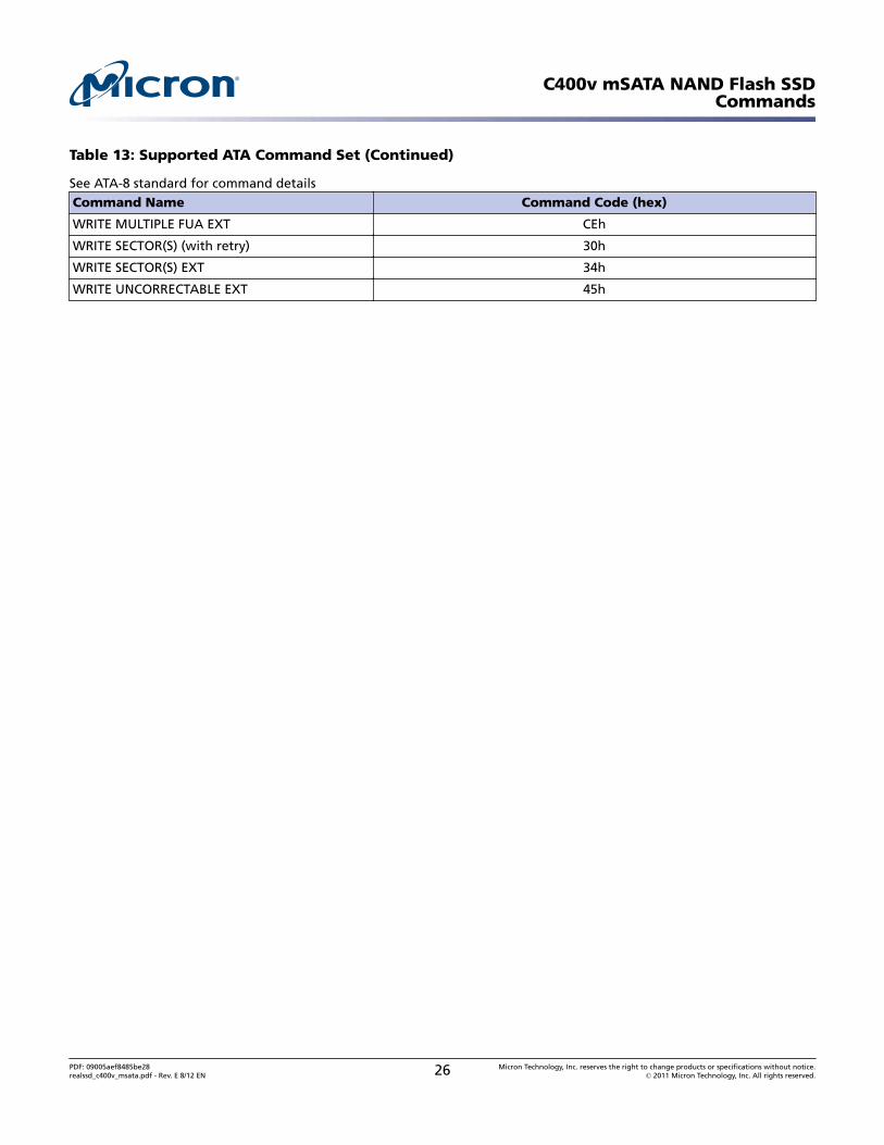
Table 13: Supported ATA Command Set (Continued)
See ATA-8 standard for command detailsCommand Name Command Code (hex)
WRITE MULTIPLE FUA EXT CEh
WRITE SECTOR(S) (with retry) 30h
WRITE SECTOR(S) EXT 34h
WRITE UNCORRECTABLE EXT 45h
C400v mSATA NAND Flash SSDCommands
PDF: 09005aef8485be28realssd_c400v_msata.pdf - Rev. E 8/12 EN 26 Micron Technology, Inc. reserves the right to change products or specifications without notice.
© 2011 Micron Technology, Inc. All rights reserved.
ComplianceMicron SSDs comply with the following:
• RoHS “green”• CE (Europe): EN55022, 2006 Class B and EN55024, 1998 + A1: 2001 + A2:2003• FCC: CFR Title 47, Part 15, ICES-003, all Class B• UL (US): approval to UL-60950-1, 2nd Edition, 2007-03-27, IEC 60950-1:2005, 2nd Ed-
ition• BSMI (Taiwan): approval to CNS 13438• C-TICK (Australia, New Zealand): approval to AS/NZS CISPR22• KCC RRL (Korea): approval to KCC MU2-C30025, KCC MU2-C30018 Class B• W.E.E.E.: Compliance with EU WEEE directive 2002/96/EC. Additional obligations
may apply to customers who place these products in the markets where WEEE is en-forced.
• TUV (Germany): approval to IEC60950/EN60950• VCCI
• IC (Canada):- This Class B digital apparatus complies with Canadian ICES-003.- Cet appareil numérique de la classe B est conforme à la norme NMB-003 du Canada.
FCC Rules
This equipment has been tested and found to comply with the limits for a Class B digitaldevice, pursuant to part 15 of the FCC Rules. These limits are designed to provide rea-sonable protection against harmful interference in a residential installation. This equip-ment generates, uses, and can radiate radio frequency energy and, if not installed andused in accordance with the instructions, may cause harmful interference to radio com-munications. However, there is no guarantee that interference will not occur in a partic-ular installation. If this equipment does cause harmful interference to radio or televi-sion reception, which can be determined by turning the equipment off and on, the useris encouraged to try to correct the interference by one or more of the following meas-ures:
• Reorient or relocate the receiving antenna.• Increase the separation between the equipment and the receiver.• Connect the equipment into an outlet on a circuit different from that to which the re-
ceiver is connected.• Consult the dealer or an experienced radio/TV technician for help.
C400v mSATA NAND Flash SSDCompliance
PDF: 09005aef8485be28realssd_c400v_msata.pdf - Rev. E 8/12 EN 27 Micron Technology, Inc. reserves the right to change products or specifications without notice.
© 2011 Micron Technology, Inc. All rights reserved.
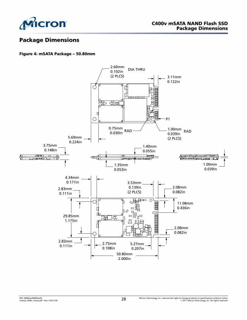
Package Dimensions
Figure 4: mSATA Package – 50.80mm
1.35mm0.053in
1.40mm0.055in
5.27mm0.207in
3.11mm0.122in
4.34mm0.171in
5.69mm0.224in
29.85mm1.175in
50.80mm2.000in
2.75mm0.108in
3.53mm0.139in(2 PLCS)
2.08mm0.082in
2.08mm0.082in
11.08mm0.436in
2.83mm0.111in
2.83mm0.111in
2.60mm0.102in(2 PLCS)
DIA THRU
1.00mm0.039in(2 PLCS)
RAD
1.00mm0.039in
0.75mm0.030in RAD
3.75mm0.148in
P1
C400v mSATA NAND Flash SSDPackage Dimensions
PDF: 09005aef8485be28realssd_c400v_msata.pdf - Rev. E 8/12 EN 28 Micron Technology, Inc. reserves the right to change products or specifications without notice.
© 2011 Micron Technology, Inc. All rights reserved.
References• Serial ATA: High-speed serialized AT attachment, Serial ATA working group, available
at www.sata-io.org• SATA 3.0 GOLD• ATA-8 ACS2• JEDEC MO-300B (mSATA SSD Assembly)
C400v mSATA NAND Flash SSDReferences
PDF: 09005aef8485be28realssd_c400v_msata.pdf - Rev. E 8/12 EN 29 Micron Technology, Inc. reserves the right to change products or specifications without notice.
© 2011 Micron Technology, Inc. All rights reserved.
Revision History
Rev. E – 8/12
• Changed MTBF to MTTF.• Added new power-off sequence note to Maximum Ratings table.• Added new note to Word 76 in Device ID table.
Rev. D – 4/12
• In Features section, removed reference to hot-plug-capable and changed caseless de-sign height from 3.80mm to 3.75mm.
• In Physical Configuration section, changed height from 3.80mm to 3.75mm.• Updated package dimensions figure (mSATA Package – 50.80mm):
– 3.80mm to 3.75mm– 0.150in to 0.148in– 1.40mm to 1.35mm– 0.055in to 0.053in
Rev. C – 3/12
• Added Cache Drive Performance table to Performance.
Rev. B – 1/12
• Added 32GB.
Rev. A – 10/11
• Initial release.
8000 S. Federal Way, P.O. Box 6, Boise, ID 83707-0006, Tel: 208-368-3900www.micron.com/productsupport Customer Comment Line: 800-932-4992
Micron and the Micron logo are trademarks of Micron Technology, Inc.All other trademarks are the property of their respective owners.
This data sheet contains minimum and maximum limits specified over the power supply and temperature range set forth herein.Although considered final, these specifications are subject to change, as further product development and data characterization some-
times occur.
C400v mSATA NAND Flash SSDRevision History
PDF: 09005aef8485be28realssd_c400v_msata.pdf - Rev. E 8/12 EN 30 Micron Technology, Inc. reserves the right to change products or specifications without notice.
© 2011 Micron Technology, Inc. All rights reserved.


![NAND Flash Memory - Digi-Key Sheets/Micron Technology Inc...nand flash memory mt29f16g08ababa, mt29f32g08afaba, mt29f64g08a[j/k/m]aba, mt29f128g08auaba, mt29f16g08abcbb, mt29f32g08aecbb,](https://img.dokumen.tips/doc/110x75/5aece0407f8b9a3b2e8fb6f1/nand-flash-memory-digi-key-sheetsmicron-technology-incnand-flash-memory-mt29f16g08ababa.jpg)