Embed Size (px)
Citation preview
TN-29-06: NAND Flash Controller on Spartan-3Overview
09005aef81962279 pdf/ 09005aef819621d4 source Micron Technology, Inc., reserves the right to change products or specifications without notice.tn2906_nand_flash_controller.fm - Rev. C 7/14 EN 1 ©2005 Micron Technology, Inc. All rights reserved.
Products and specifications discussed herein are for evaluation and reference purposes only and are subject to change by Micron without notice. Products are only warranted by Micron to meet Micron’s production data sheet specifications. All
information discussed herein is provided on an “as is” basis, without warranties of any kind.
Technical NoteMicron NAND Flash Controller via Xilinx Spartan-3 FPGA
OverviewAs mobile product capabilities continue to expand, so does the demand for high-density static memory storage. NAND Flash memory is moving to the forefront, evolving rapidly to meet this ever-growing demand. Micron offers designers a complete solution that includes industry-standard NAND features, Micron enhancements, plus software and support options.
NAND Flash architecture differs from that of traditional memory sources, so accessing a NAND Flash device from a host presents challenges for systems designers. The most direct approach for a host interface is using a NAND Flash controller. The NAND Flash controller can be an internal device, built into the application processor or host, or designs can incorporate an external, stand-alone chip.
This technical note describes the Micron NAND Flash controller, techniques for inter-facing the NAND Flash device with a processor (using Xilinx Spartan-3 as an exam-ple), and use of the Micron glueless interface to interface a processor with NAND Flash memory.
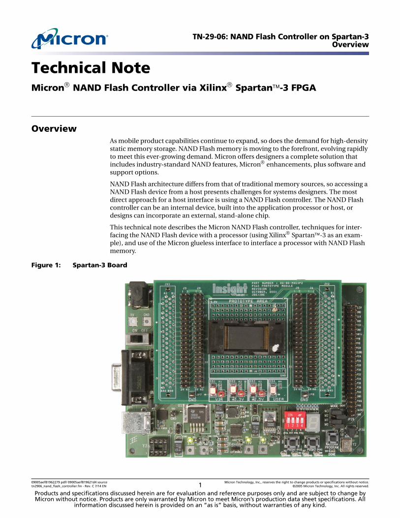
Figure 1: Spartan-3 Board
09005aef81962279 pdf/ 09005aef819621d4 source Micron Technology, Inc., reserves the right to change products or specifications without notice.tn2906_nand_flash_controller.fm - Rev. C 7/14 EN 2 ©2005 Micron Technology, Inc. All rights reserved.
TN-29-06: NAND Flash Controller on Spartan-3Overview
Interface Options
In situations where the processor lacks a native NAND Flash controller, it is possible to design a simple memory-mapped interface providing a hardware interface to the NAND Flash device. This gives NAND Flash the appearance of an SRAM when interfaced to a processor, microcontroller, or any other host device.
ECC Requirement
To protect against bit errors, error correction code (ECC) is an essential part of the NAND Flash interface. The Micron ECC module technical note (TN-29-05) provides a thorough review of error correction for NAND Flash.
The Micron NAND Flash controller is designed to work in series, with the optional Micron NAND Flash ECC module placed between the NAND Flash controller and the NAND Flash device. Throughout this document, the presence of an ECC module is assumed.
Development and Testing
The Micron NAND Flash controller was developed and tested using the Xilinx Spartan-3 board and can be ported to other platforms of the user’s choosing.
09005aef81962279 pdf/ 09005aef819621d4 source Micron Technology, Inc., reserves the right to change products or specifications without notice.tn2906_nand_flash_controller.fm - Rev. C 7/14 EN 3 ©2005 Micron Technology, Inc. All rights reserved.
TN-29-06: NAND Flash Controller on Spartan-3NAND Flash Controller Design and Implementation
NAND Flash Controller Design and ImplementationThe Micron NAND Flash controller is designed and implemented using the following hardware and software:• Xilinx Spartan-3 board• Memec Insight Prototype P160 board with 48-pin TSOP socket• Xilinx ISE 6.2i• Xilinx Platform Studio• Xilinx Impact• Xilinx XMD• ModelSim
• Micron 2Gb NAND Flash device (also functional for 4Gb and 8Gb x8/x16 devices)
Micron NAND Flash Controller FeaturesOrganization:• 2 buffers—2,112 bytes each• Standard memory-mapped interface• NAND Flash interface• 16 command registers
Performance:• Double buffering enables host to read and write concurrently• Synchronous READs at 100 MHz• Asynchronous READs with 10ns delay• Synchronous WRITEs at 100 MHz• Maximum rated clock speed of 100 MHz
Standard NAND Command Support:• Memory-mapped I/O input registers • Status and ID registers• Host interrupts on completion
Error Correction:• ECC module (optional)• Controller that reads errors and corrects them• Status register that is also used for ECC status• errINT line used to handle errors
09005aef81962279 pdf/ 09005aef819621d4 source Micron Technology, Inc., reserves the right to change products or specifications without notice.tn2906_nand_flash_controller.fm - Rev. C 7/14 EN 4 ©2005 Micron Technology, Inc. All rights reserved.
TN-29-06: NAND Flash Controller on Spartan-3Micron NAND Flash Controller Features
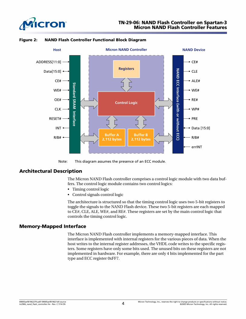
Figure 2: NAND Flash Controller Functional Block Diagram
Note: This diagram assumes the presence of an ECC module.
Architectural Description
The Micron NAND Flash controller comprises a control logic module with two data buf-fers. The control logic module contains two control logics:• Timing control logic• Control signals control logic
The architecture is structured so that the timing control logic uses two 5-bit registers to toggle the signals to the NAND Flash device. These two 5-bit registers are each mapped to CE#, CLE, ALE, WE#, and RE#. These registers are set by the main control logic that controls the timing control logic.
Memory-Mapped Interface
The Micron NAND Flash controller implements a memory-mapped interface. This interface is implemented with internal registers for the various pieces of data. When the host writes to the internal register addresses, the VHDL code writes to the specific regis-ters. Some registers have only some bits used. The unused bits on these registers are not implemented in hardware. For example, there are only 4 bits implemented for the part type and ECC register 0xFF7.
Buffer A2,112 bytes
Registers
Buffer B2,112 bytes
Stand
ard SR
AM
Interface
NA
ND
ECC
Interface (w
ith o
r with
ou
t ECC
)
Control Logic
ADDRESS[11:0]
Data[15:0]
CE#
WE#
OE#
CLK
RESET#
INT
R/B#
CE#
CLE
ALE#
WE#
RE#
WP#
PRE
Data [15:0]
R/B#
errINT
Micron NAND Controller NAND DeviceHost
09005aef81962279 pdf/ 09005aef819621d4 source Micron Technology, Inc., reserves the right to change products or specifications without notice.tn2906_nand_flash_controller.fm - Rev. C 7/14 EN 5 ©2005 Micron Technology, Inc. All rights reserved.
TN-29-06: NAND Flash Controller on Spartan-3Micron NAND Flash Controller Features
Timing Control Logic
The control logic is divided structurally into two VHDL processes (see Figure 4 on page 10 and Figure 5 on page 11).
The timing control logic generates a 60ns clock with a 33.33 percent duty cycle (for example, 40ns LOW and 20ns HIGH). This duty cycle is generated using a delay counter that counts from “0” to “5.” The delay counter keeps the signal LOW when the counter is “0,” “1,” “2,” or “3” and HIGH when it is “4” or “5.” Thus, it keeps the first output vector for 40ns and the second for 20ns.
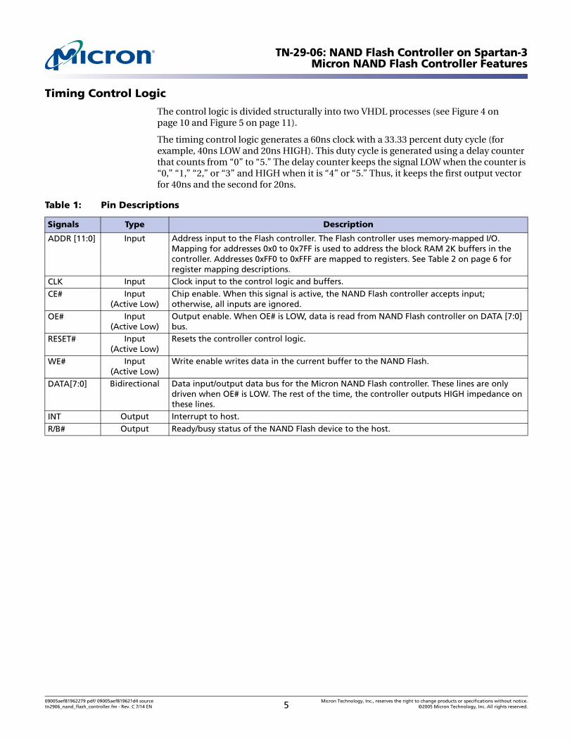
Table 1: Pin Descriptions
Signals Type Description
ADDR [11:0] Input Address input to the Flash controller. The Flash controller uses memory-mapped I/O. Mapping for addresses 0x0 to 0x7FF is used to address the block RAM 2K buffers in the controller. Addresses 0xFF0 to 0xFFF are mapped to registers. See Table 2 on page 6 for register mapping descriptions.
CLK Input Clock input to the control logic and buffers.
CE# Input(Active Low)
Chip enable. When this signal is active, the NAND Flash controller accepts input; otherwise, all inputs are ignored.
OE# Input(Active Low)
Output enable. When OE# is LOW, data is read from NAND Flash controller on DATA [7:0] bus.
RESET# Input(Active Low)
Resets the controller control logic.
WE# Input(Active Low)
Write enable writes data in the current buffer to the NAND Flash.
DATA[7:0] Bidirectional Data input/output data bus for the Micron NAND Flash controller. These lines are only driven when OE# is LOW. The rest of the time, the controller outputs HIGH impedance on these lines.
INT Output Interrupt to host.
R/B# Output Ready/busy status of the NAND Flash device to the host.
09005aef81962279 pdf/ 09005aef819621d4 source Micron Technology, Inc., reserves the right to change products or specifications without notice.tn2906_nand_flash_controller.fm - Rev. C 7/14 EN 6 ©2005 Micron Technology, Inc. All rights reserved.
TN-29-06: NAND Flash Controller on Spartan-3Micron NAND Flash Controller Features
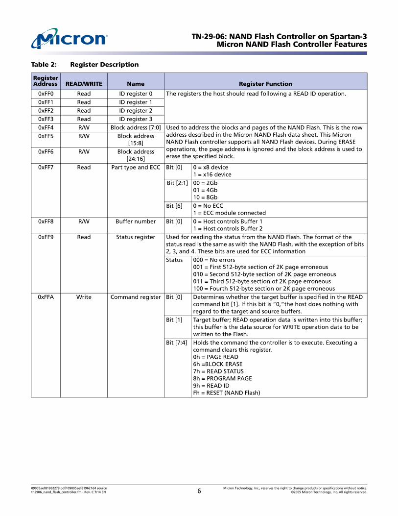
Table 2: Register Description
Register Address READ/WRITE Name Register Function
0xFF0 Read ID register 0 The registers the host should read following a READ ID operation.0xFF1 Read ID register 10xFF2 Read ID register 20xFF3 Read ID register 30xFF4 R/W Block address [7:0] Used to address the blocks and pages of the NAND Flash. This is the row
address described in the Micron NAND Flash data sheet. This Micron NAND Flash controller supports all NAND Flash devices. During ERASE operations, the page address is ignored and the block address is used to erase the specified block.
0xFF5 R/W Block address [15:8]
0xFF6 R/W Block address [24:16]
0xFF7 Read Part type and ECC Bit [0] 0 = x8 device1 = x16 device
Bit [2:1] 00 = 2Gb01 = 4Gb10 = 8Gb
Bit [6] 0 = No ECC1 = ECC module connected
0xFF8 R/W Buffer number Bit [0] 0 = Host controls Buffer 11 = Host controls Buffer 2
0xFF9 Read Status register Used for reading the status from the NAND Flash. The format of the status read is the same as with the NAND Flash, with the exception of bits 2, 3, and 4. These bits are used for ECC informationStatus 000 = No errors
001 = First 512-byte section of 2K page erroneous010 = Second 512-byte section of 2K page erroneous011 = Third 512-byte section of 2K page erroneous100 = Fourth 512-byte section or 2K page erroneous
0xFFA Write Command register Bit [0] Determines whether the target buffer is specified in the READ command bit [1]. If this bit is “0,”the host does nothing with regard to the target and source buffers.
Bit [1] Target buffer; READ operation data is written into this buffer; this buffer is the data source for WRITE operation data to be written to the Flash.
Bit [7:4] Holds the command the controller is to execute. Executing a command clears this register.0h = PAGE READ6h =BLOCK ERASE7h = READ STATUS8h = PROGRAM PAGE9h = READ IDFh = RESET (NAND Flash)
09005aef81962279 pdf/ 09005aef819621d4 source Micron Technology, Inc., reserves the right to change products or specifications without notice.tn2906_nand_flash_controller.fm - Rev. C 7/14 EN 7 ©2005 Micron Technology, Inc. All rights reserved.
TN-29-06: NAND Flash Controller on Spartan-3READ Operations
READ Operations
PAGE READ Operation
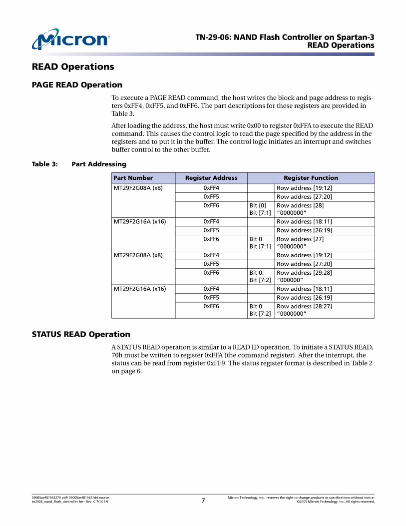
To execute a PAGE READ command, the host writes the block and page address to regis-ters 0xFF4, 0xFF5, and 0xFF6. The part descriptions for these registers are provided in Table 3.
After loading the address, the host must write 0x00 to register 0xFFA to execute the READ command. This causes the control logic to read the page specified by the address in the registers and to put it in the buffer. The control logic initiates an interrupt and switches buffer control to the other buffer.
STATUS READ Operation
A STATUS READ operation is similar to a READ ID operation. To initiate a STATUS READ, 70h must be written to register 0xFFA (the command register). After the interrupt, the status can be read from register 0xFF9. The status register format is described in Table 2 on page 6.
Table 3: Part Addressing
Part Number Register Address Register Function
MT29F2G08A (x8) 0xFF4 Row address [19:12]0xFF5 Row address [27:20]0xFF6 Bit [0]
Bit [7:1]Row address [28]“0000000”
MT29F2G16A (x16) 0xFF4 Row address [18:11]0xFF5 Row address [26:19]0xFF6 Bit 0
Bit [7:1]Row address [27]“0000000”
MT29F2G08A (x8) 0xFF4 Row address [19:12]0xFF5 Row address [27:20]0xFF6 Bit 0:
Bit [7:2]Row address [29:28]“000000”
MT29F2G16A (x16) 0xFF4 Row address [18:11]0xFF5 Row address [26:19]0xFF6 Bit 0
Bit [7:2] Row address [28:27]“0000000”
09005aef81962279 pdf/ 09005aef819621d4 source Micron Technology, Inc., reserves the right to change products or specifications without notice.tn2906_nand_flash_controller.fm - Rev. C 7/14 EN 8 ©2005 Micron Technology, Inc. All rights reserved.
TN-29-06: NAND Flash Controller on Spartan-3Micron NAND Flash Controller Design Details
Micron NAND Flash Controller Design Details
Controller Timing
Micron recommends a 100 MHz clock period for the controller, or a clock cycle time of 10ns. This enables adjustment of the NAND Flash interface to the required timing. The fastest the controller can toggle the NAND Flash is a 20 MHz clock period and a 50ns clock cycle time. Data is assured to be valid 35ns after the falling edge of RE#. Data is also assured to be valid at least 10ns after the rising edge of RE#. Thus, if the clock is 50 Mhz with a 40 percent duty cycle, the result is a 30ns LOW strobe. The data would need to be sampled at 35ns from the falling edge of RE#, which is not recommended, as the data may become valid, failing to allow adequate register or latch setup time. To provide a margin of error, a 60ns clock cycle with a 33.33 percent duty cycle is specified.
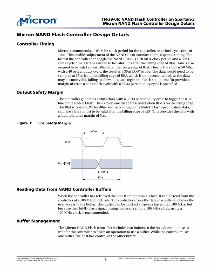
Output Safety Margin
The controller generates a 60ns clock with a 33.33 percent duty cycle to toggle the RE# line of the NAND Flash. This is to ensure that data is valid when RE# is on the rising edge. The RE# strobe is LOW for 40ns and, according to the NAND Flash specification data, can take 35ns at most to be valid after the falling edge of RE#. This provides the data with a fault tolerance margin of 5ns.
Figure 3: 5ns Safety Margin
Reading Data from NAND Controller Buffers
When the controller has retrieved the data from the NAND Flash, it can be read from the controller at a 100 MHz clock rate. The controller stores the data in a buffer and gives the user access to the buffer. This buffer can be clocked at speeds faster than 100 MHz, but because the NAND Flash signal timing has been set for a 100 MHz clock, using a 100 MHz clock is recommended.
Buffer Management
The Micron NAND Flash controller includes two buffers so the host does not have to wait for the controller to finish an operation to use a buffer. While the controller uses one buffer, the host has control of the other buffer.
40ns
60ns
5ns
RE#
Data[7:0]
09005aef81962279 pdf/ 09005aef819621d4 source Micron Technology, Inc., reserves the right to change products or specifications without notice.tn2906_nand_flash_controller.fm - Rev. C 7/14 EN 9 ©2005 Micron Technology, Inc. All rights reserved.
TN-29-06: NAND Flash Controller on Spartan-3Micron NAND Flash Controller Design Details
When the host issues a WRITE command, the buffer that the host controls is taken over by the controller, and the host then takes control of the other buffer. At this point, the controller reads from the host-controlled buffer and writes to NAND Flash memory; at the same time, the user can employ the other buffer.
When the host issues a READ command, the controller reads the data into the buffer the user is not accessing. At the end of the READ operation, the controller automatically switches host control to the buffer containing the data read from NAND Flash. This switch is implemented so that the user can choose to not engage the double buffering feature. However, if the host contains some valuable data in the other buffer, it is pre-served; the user can continue to use that buffer by changing buffer control to the desired buffer. Changing buffer control is carried out by reading and writing to the register at address 0xFF8.
Double Address Buffering
In addition to its two controller buffers, the Micron NAND Flash controller also has two address buffers. For example, the registers at addresses 0xFF4, 0xFF5, and 0xFF6 are double buffered.
Unlike the data buffers, the user cannot manually change control of the address buffers. However, the host can check which address buffer it controls by reading bit 1 from the register at address 0xFF8.
The Micron NAND Flash controller makes it possible for the host to work with one data buffer while the controller uses the other data buffer. This is done with the address buf-fers, as if the control logic is using the address buffers. The host should not write to the same address buffer the controller is using. Therefore, every time the host issues a com-mand that requires the address buffer, the controller switches user control to the other address buffer, preventing the user from interfering with the buffer used for the NAND bus addressing.
After the host issues a READ or a WRITE command, the controller takes control of the buffer that the host was controlling when the command was issued. At this point, the host gets new flushed buffers for the address. This enables the user to enter a new address while the controller is reading the address from another set of address buffers.
Double Data Buffering
The Micron NAND Flash controller has two 2,112-byte data buffers. These buffers are implemented so that a user always has a buffer to read from and write to. As shown in the block diagram in Figure 2 on page 4, the two buffers are referred to as buffer A and buffer B.
During a READ operation, if the user controls buffer A before the READ operation, when the controller is finished, it will automatically switch user control to buffer B. If the user has valid data in buffer A, it will be preserved. The user can manually switch control back to the other buffer by writing to register 0xFF8.
During a WRITE operation, if the user controls buffer A before the WRITE operation, the controller assumes that the buffer that needed to be written to NAND Flash is buffer A. The controller takes control of buffer A as soon as the PROGRAM operation is issued and automatically gives the user control of buffer B.
The host can also specify the buffer in which a READ or a WRITE will execute.
09005aef81962279 pdf/ 09005aef819621d4 source Micron Technology, Inc., reserves the right to change products or specifications without notice.tn2906_nand_flash_controller.fm - Rev. C 7/14 EN 10 ©2005 Micron Technology, Inc. All rights reserved.
TN-29-06: NAND Flash Controller on Spartan-3Micron NAND Flash Controller Design Details
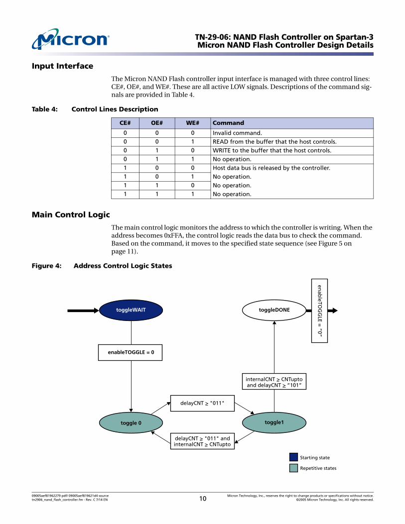
Input Interface
The Micron NAND Flash controller input interface is managed with three control lines: CE#, OE#, and WE#. These are all active LOW signals. Descriptions of the command sig-nals are provided in Table 4.
Main Control Logic
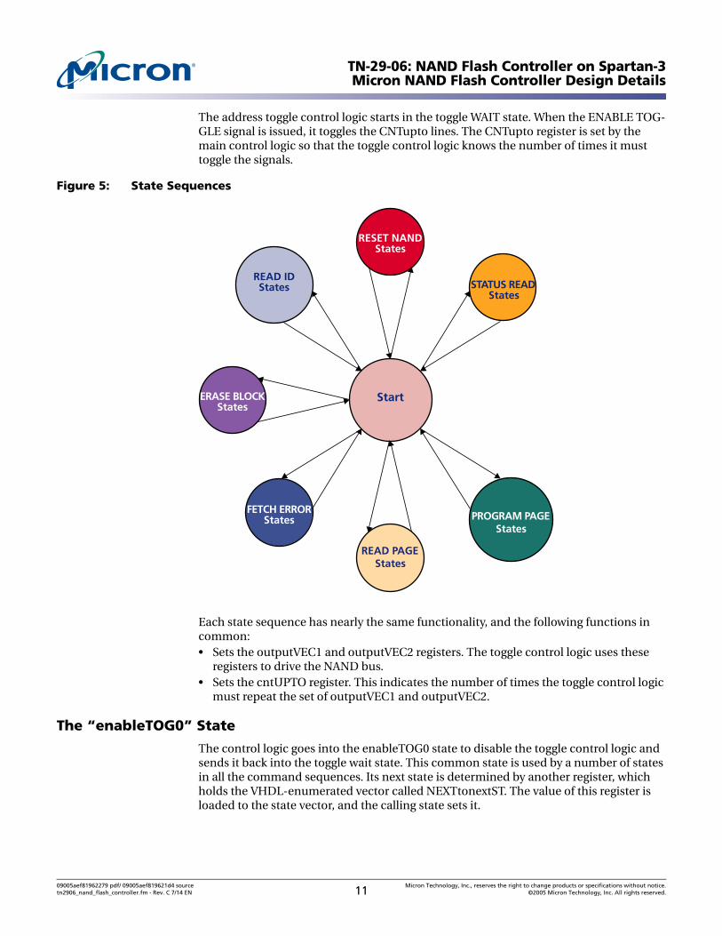
The main control logic monitors the address to which the controller is writing. When the address becomes 0xFFA, the control logic reads the data bus to check the command. Based on the command, it moves to the specified state sequence (see Figure 5 on page 11).
Figure 4: Address Control Logic States
Table 4: Control Lines Description
CE# OE# WE# Command
0 0 0 Invalid command.0 0 1 READ from the buffer that the host controls.0 1 0 WRITE to the buffer that the host controls.0 1 1 No operation.1 0 0 Host data bus is released by the controller.1 0 1 No operation.1 1 0 No operation.1 1 1 No operation.
toggleWAIT
enableTOGGLE = 0
toggle 0
toggleDONE
internalCNT > CNTuptoand delayCNT > “101”
toggle1
delayCNT > "011"
delayCNT > "011" andinternalCNT > CNTupto
enab
leTOG
GLE =
“0”
Starting state
Repetitive states
09005aef81962279 pdf/ 09005aef819621d4 source Micron Technology, Inc., reserves the right to change products or specifications without notice.tn2906_nand_flash_controller.fm - Rev. C 7/14 EN 11 ©2005 Micron Technology, Inc. All rights reserved.
TN-29-06: NAND Flash Controller on Spartan-3Micron NAND Flash Controller Design Details
The address toggle control logic starts in the toggle WAIT state. When the ENABLE TOG-GLE signal is issued, it toggles the CNTupto lines. The CNTupto register is set by the main control logic so that the toggle control logic knows the number of times it must toggle the signals.
Figure 5: State Sequences
Each state sequence has nearly the same functionality, and the following functions in common:• Sets the outputVEC1 and outputVEC2 registers. The toggle control logic uses these
registers to drive the NAND bus.• Sets the cntUPTO register. This indicates the number of times the toggle control logic
must repeat the set of outputVEC1 and outputVEC2.
The “enableTOG0” State
The control logic goes into the enableTOG0 state to disable the toggle control logic and sends it back into the toggle wait state. This common state is used by a number of states in all the command sequences. Its next state is determined by another register, which holds the VHDL-enumerated vector called NEXTtonextST. The value of this register is loaded to the state vector, and the calling state sets it.
Start
RESET NANDStates
STATUS READStates
FETCH ERRORStates PROGRAM PAGE
States
ERASE BLOCKStates
READ IDStates
READ PAGEStates
09005aef81962279 pdf/ 09005aef819621d4 source Micron Technology, Inc., reserves the right to change products or specifications without notice.tn2906_nand_flash_controller.fm - Rev. C 7/14 EN 12 ©2005 Micron Technology, Inc. All rights reserved.
TN-29-06: NAND Flash Controller on Spartan-3Micron NAND Flash Controller Design Details
R/B# Wait States
The R/B# wait states are as follows:• STwaitforRB0: This state waits for the R/B# signal to go LOW.• STwaitforRB1: This state waits for the R/B# signal to go HIGH.
Each of these states uses the NEXTtonextST register to determine the next state.
ECC Enable/Disable Mechanism
The Micron NAND Flash controller can be connected in series with the Micron ECC module. The Micron ECC module can be enabled or disabled by a signal from the Micron NAND Flash controller. The ECC module can be enabled or disabled by writing to address 0xFF7—the part type and ECC register. If the module is enabled, the control-ler writes only 2,100 bytes, leaving the last 12 bytes for the ECC module to write; other-wise, the controller writes 2,112 bytes.
The enable and disable mechanism ties the ECCpresent 1-bit register to the enable line of the ECC module. There is also a combination signal, based on the ECCpresent regis-ter, which is used to select between the values 2,100 (834h) and 2,112 (840h). If the ECCpresent register is “1,” it selects 834h; otherwise, it selects 840h.
Read Page States
The read page state sequence is more complicated than the rest because it has the error correction routines built into it. The read page sequence can be bypassed by disabling the ECC, but the states still remain there, as the ECC disable function is implemented as a software switch.
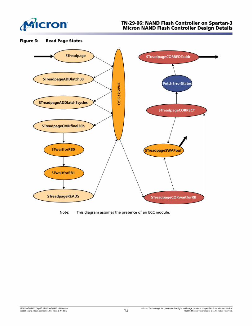
09005aef81962279 pdf/ 09005aef819621d4 source Micron Technology, Inc., reserves the right to change products or specifications without notice.tn2906_nand_flash_controller.fm - Rev. C 7/14 EN 13 ©2005 Micron Technology, Inc. All rights reserved.
TN-29-06: NAND Flash Controller on Spartan-3Micron NAND Flash Controller Design Details
Figure 6: Read Page States
Note: This diagram assumes the presence of an ECC module.
STreadpage
STreadpageADDlatch00
STreadpageADDlatch3cycles
STreadpageCMDfinal30h
STwaitforRB0
STwaitforRB1
STreadpageREADS
enab
leTOG
O
STreadpageCORREDTaddr
FetchErrorStates
STreadpageCORRECT
STreadpageSWAPbuf
STreadpageCORwaitforRB
09005aef81962279 pdf/ 09005aef819621d4 source Micron Technology, Inc., reserves the right to change products or specifications without notice.tn2906_nand_flash_controller.fm - Rev. C 7/14 EN 14 ©2005 Micron Technology, Inc. All rights reserved.
TN-29-06: NAND Flash Controller on Spartan-3Micron NAND Flash Controller Design Details
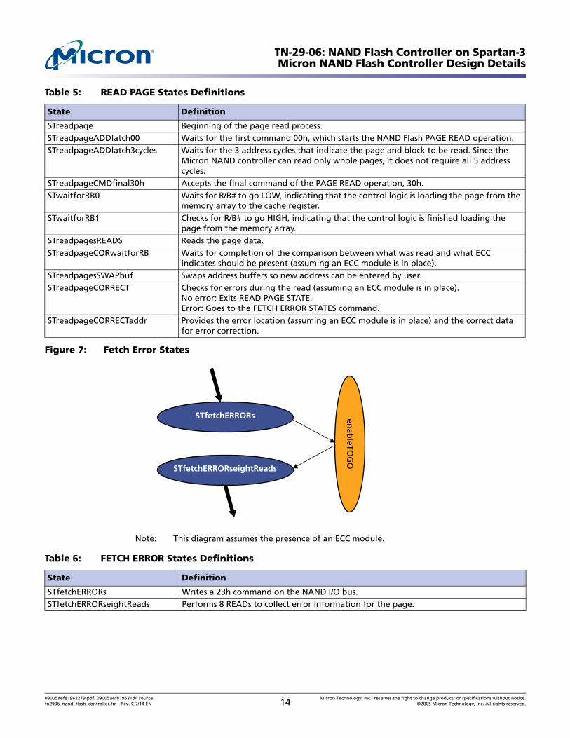
Figure 7: Fetch Error States
Note: This diagram assumes the presence of an ECC module.
Table 5: READ PAGE States Definitions
State Definition
STreadpage Beginning of the page read process.STreadpageADDlatch00 Waits for the first command 00h, which starts the NAND Flash PAGE READ operation.STreadpageADDlatch3cycles Waits for the 3 address cycles that indicate the page and block to be read. Since the
Micron NAND controller can read only whole pages, it does not require all 5 address cycles.
STreadpageCMDfinal30h Accepts the final command of the PAGE READ operation, 30h.STwaitforRB0 Waits for R/B# to go LOW, indicating that the control logic is loading the page from the
memory array to the cache register.STwaitforRB1 Checks for R/B# to go HIGH, indicating that the control logic is finished loading the
page from the memory array.STreadpagesREADS Reads the page data.STreadpageCORwaitforRB Waits for completion of the comparison between what was read and what ECC
indicates should be present (assuming an ECC module is in place).STreadpagesSWAPbuf Swaps address buffers so new address can be entered by user.STreadpageCORRECT Checks for errors during the read (assuming an ECC module is in place).
No error: Exits READ PAGE STATE. Error: Goes to the FETCH ERROR STATES command.
STreadpageCORRECTaddr Provides the error location (assuming an ECC module is in place) and the correct data for error correction.
Table 6: FETCH ERROR States Definitions
State Definition
STfetchERRORs Writes a 23h command on the NAND I/O bus.STfetchERRORseightReads Performs 8 READs to collect error information for the page.
STfetchERRORs
STfetchERRORseightReads
enab
leTOG
O
09005aef81962279 pdf/ 09005aef819621d4 source Micron Technology, Inc., reserves the right to change products or specifications without notice.tn2906_nand_flash_controller.fm - Rev. C 7/14 EN 15 ©2005 Micron Technology, Inc. All rights reserved.
TN-29-06: NAND Flash Controller on Spartan-3Micron NAND Flash Controller Design Details
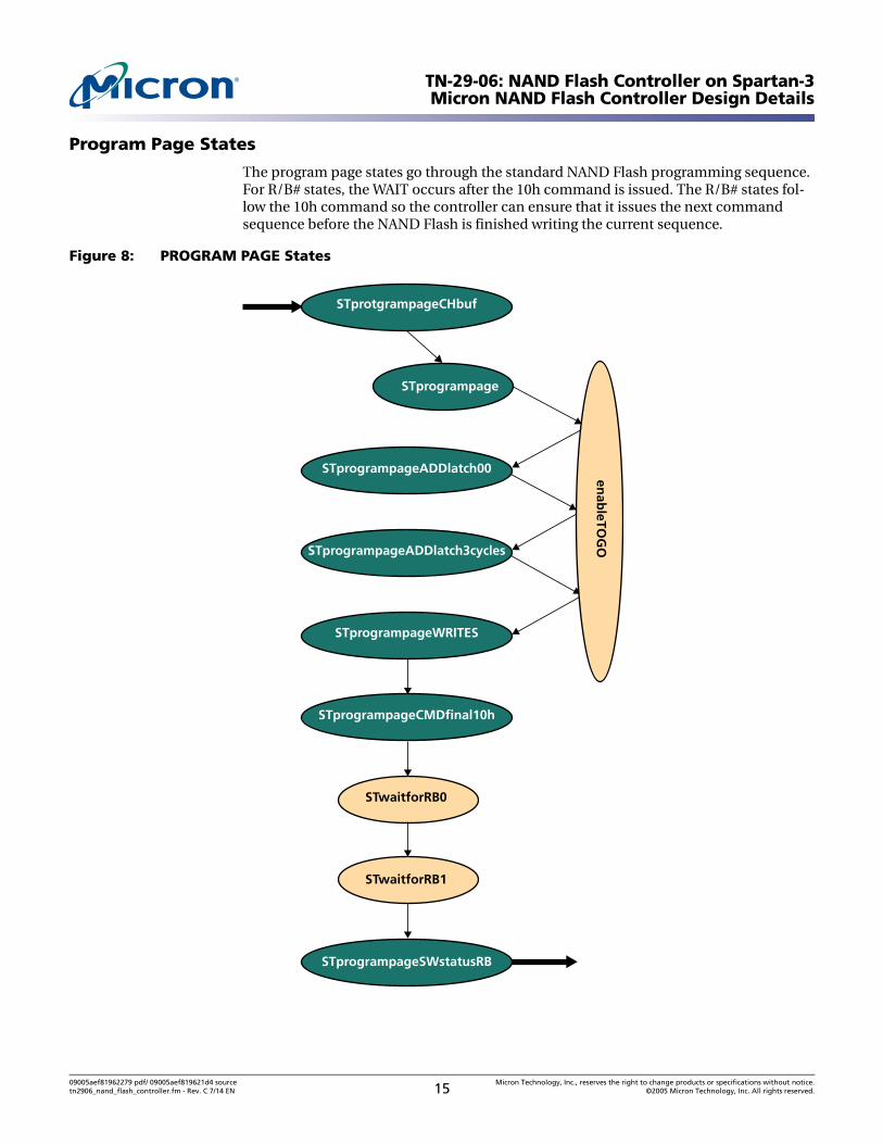
Program Page States
The program page states go through the standard NAND Flash programming sequence. For R/B# states, the WAIT occurs after the 10h command is issued. The R/B# states fol-low the 10h command so the controller can ensure that it issues the next command sequence before the NAND Flash is finished writing the current sequence.
Figure 8: PROGRAM PAGE States
STprotgrampageCHbuf
STprogrampage
STprogrampageADDlatch00
STprogrampageADDlatch3cycles
STprogrampageWRITES
STprogrampageCMDfinal10h
STwaitforRB0
STwaitforRB1
STprogrampageSWstatusRB
enab
leTOG
O
09005aef81962279 pdf/ 09005aef819621d4 source Micron Technology, Inc., reserves the right to change products or specifications without notice.tn2906_nand_flash_controller.fm - Rev. C 7/14 EN 16 ©2005 Micron Technology, Inc. All rights reserved.
TN-29-06: NAND Flash Controller on Spartan-3Micron NAND Flash Controller Design Details
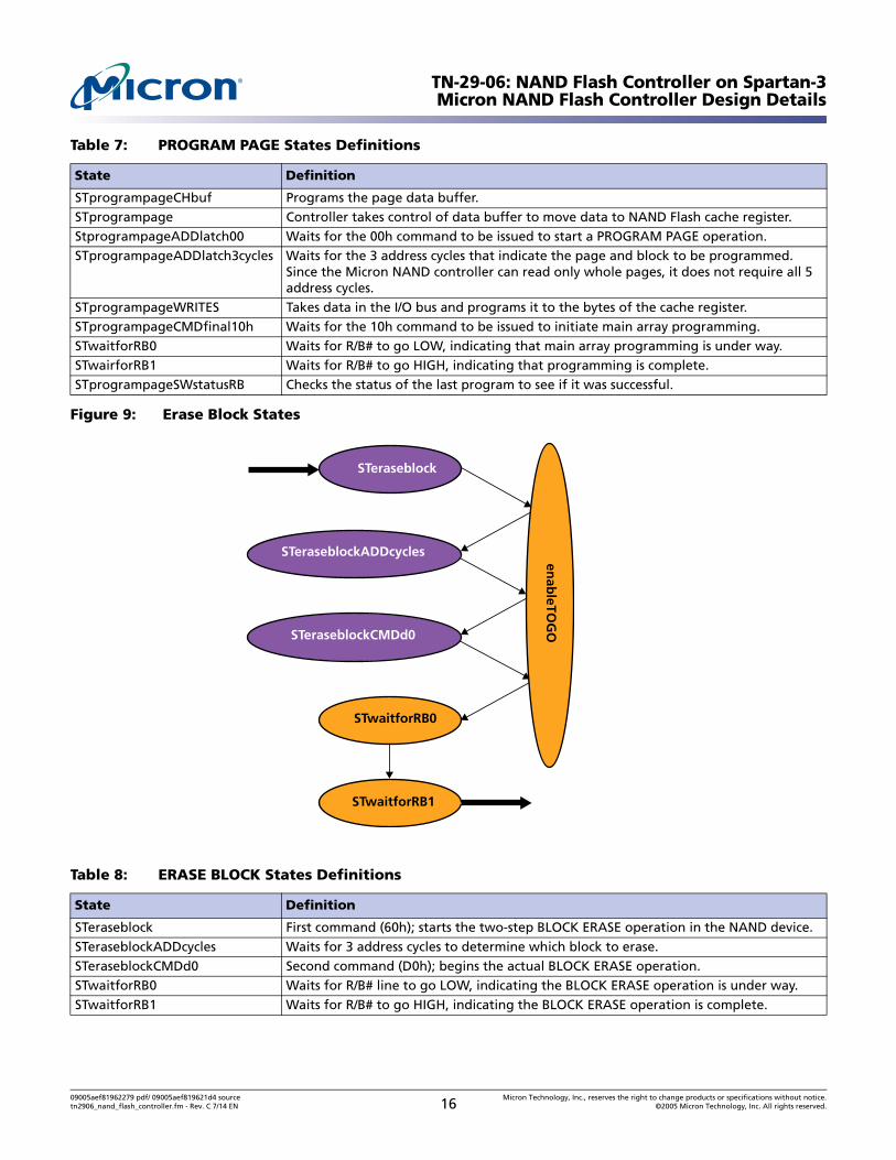
Figure 9: Erase Block States
Table 7: PROGRAM PAGE States Definitions
State Definition
STprogrampageCHbuf Programs the page data buffer.STprogrampage Controller takes control of data buffer to move data to NAND Flash cache register.StprogrampageADDlatch00 Waits for the 00h command to be issued to start a PROGRAM PAGE operation.STprogrampageADDlatch3cycles Waits for the 3 address cycles that indicate the page and block to be programmed.
Since the Micron NAND controller can read only whole pages, it does not require all 5 address cycles.
STprogrampageWRITES Takes data in the I/O bus and programs it to the bytes of the cache register.STprogrampageCMDfinal10h Waits for the 10h command to be issued to initiate main array programming.STwaitforRB0 Waits for R/B# to go LOW, indicating that main array programming is under way.STwairforRB1 Waits for R/B# to go HIGH, indicating that programming is complete.STprogrampageSWstatusRB Checks the status of the last program to see if it was successful.
Table 8: ERASE BLOCK States Definitions
State Definition
STeraseblock First command (60h); starts the two-step BLOCK ERASE operation in the NAND device.STeraseblockADDcycles Waits for 3 address cycles to determine which block to erase.STeraseblockCMDd0 Second command (D0h); begins the actual BLOCK ERASE operation.STwaitforRB0 Waits for R/B# line to go LOW, indicating the BLOCK ERASE operation is under way.STwaitforRB1 Waits for R/B# to go HIGH, indicating the BLOCK ERASE operation is complete.
STeraseblock
STeraseblockADDcycles
STeraseblockCMDd0
STwaitforRB0
STwaitforRB1
enab
leTOG
O
09005aef81962279 pdf/ 09005aef819621d4 source Micron Technology, Inc., reserves the right to change products or specifications without notice.tn2906_nand_flash_controller.fm - Rev. C 7/14 EN 17 ©2005 Micron Technology, Inc. All rights reserved.
TN-29-06: NAND Flash Controller on Spartan-3Micron NAND Flash Controller Design Details
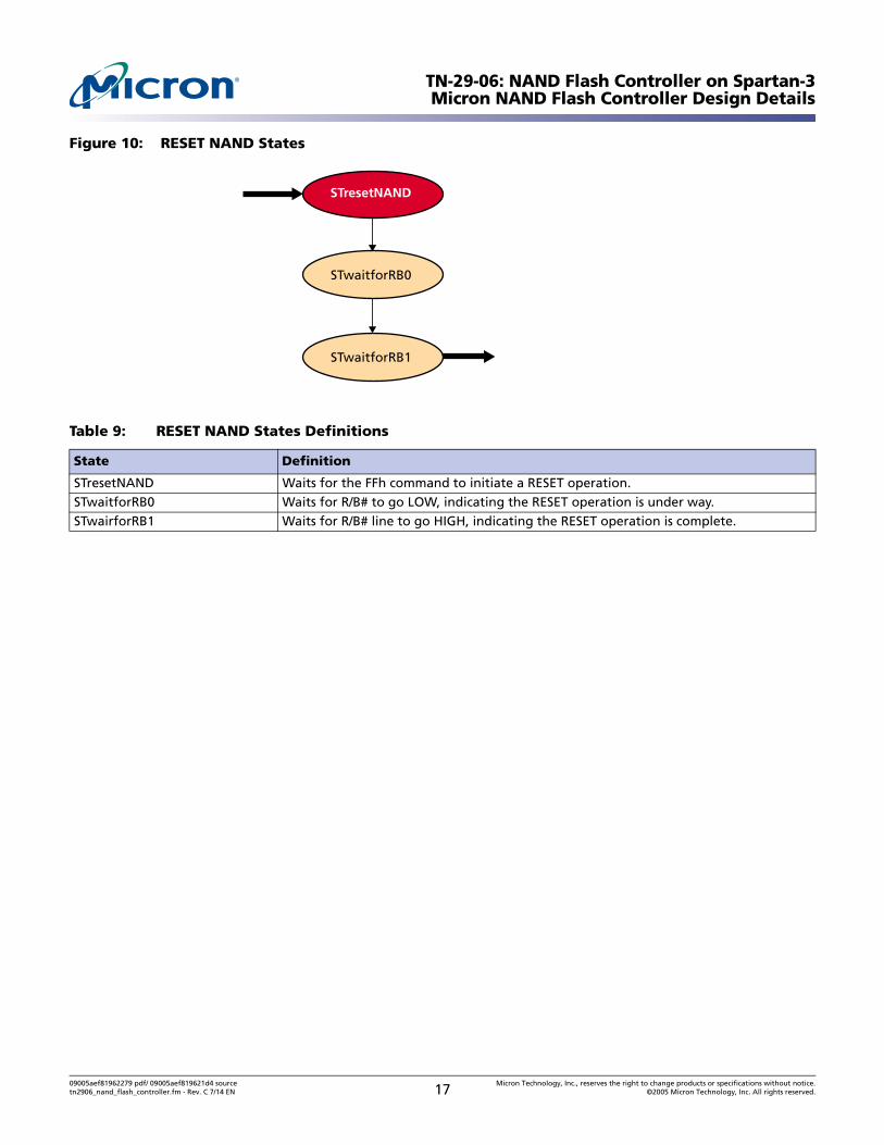
Figure 10: RESET NAND States
Table 9: RESET NAND States Definitions
State Definition
STresetNAND Waits for the FFh command to initiate a RESET operation.STwaitforRB0 Waits for R/B# to go LOW, indicating the RESET operation is under way.STwairforRB1 Waits for R/B# line to go HIGH, indicating the RESET operation is complete.
STresetNAND
STwaitforRB0
STwaitforRB1
09005aef81962279 pdf/ 09005aef819621d4 source Micron Technology, Inc., reserves the right to change products or specifications without notice.tn2906_nand_flash_controller.fm - Rev. C 7/14 EN 18 ©2005 Micron Technology, Inc. All rights reserved.
TN-29-06: NAND Flash Controller on Spartan-3Micron NAND Flash Controller Design Details
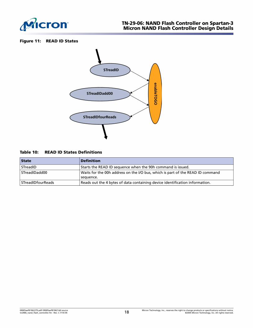
Figure 11: READ ID States
Table 10: READ ID States Definitions
State Definition
STreadID Starts the READ ID sequence when the 90h command is issued.STreadIDadd00 Waits for the 00h address on the I/O bus, which is part of the READ ID command
sequence.STreadIDfourReads Reads out the 4 bytes of data containing device identification information.
STreadID
STreadIDadd00
STreadIDfourReads
enab
leTOG
O
09005aef81962279 pdf/ 09005aef819621d4 source Micron Technology, Inc., reserves the right to change products or specifications without notice.tn2906_nand_flash_controller.fm - Rev. C 7/14 EN 19 ©2005 Micron Technology, Inc. All rights reserved.
TN-29-06: NAND Flash Controller on Spartan-3Micron NAND Flash Controller Design Details
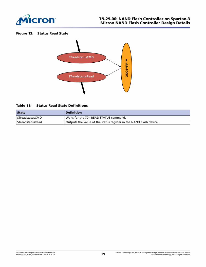
Figure 12: Status Read State
Table 11: Status Read State Definitions
State Definition
STreadstatusCMD Waits for the 70h READ STATUS command.STreadstatusRead Outputs the value of the status register in the NAND Flash device.
STreadstatusCMD
STreadstatusReaden
ableTO
GO
09005aef81962279 pdf/ 09005aef819621d4 source Micron Technology, Inc., reserves the right to change products or specifications without notice.tn2906_nand_flash_controller.fm - Rev. C 7/14 EN 20 ©2005 Micron Technology, Inc. All rights reserved.
TN-29-06: NAND Flash Controller on Spartan-3Limitations *************
Limitations *************
Paging and Partial-Page WRITEs
The Micron NAND Flash ECC controller does not support partial-page WRITEs. When the PROGRAM command is issued, the controller takes whatever is in the buffer and writes it to the NAND Flash. Therefore, the host should fill in “1” at each location where no data is to be written to the page.
Bad-Block Management
The Micron NAND Flash controller does not perform bad-block management in hard-ware, as this is a software function. The Micron NAND Flash specification requires that a bad block be marked “bad” at the factory, by writing a byte other than 0xFF into byte 2,048 (the first byte of the extra space) of page 0 or page 1 of the bad block. Precautions should be taken to ensure that bad blocks are not inadvertently left unmarked by removal of the “bad” marking. When the bad-block mark is lost (for example, by erasing a bad block without a mechanism for recording its location), its location cannot be retrieved again, and a malfunction may result.
ECC Module
Using the Micron NAND Flash Controller with the Micron ECC Module
The Micron ECC module uses the standard NAND Flash interface, with interrupt and enable lines added on the host side. This interface plugs directly into the Micron NAND Flash controller and can also be used to easily make a glueless interface with built-in ECC.
If the controller is being used with the ECC module, it gives the host the ECC debug fea-ture of reading the 8 bytes of error information from the ECC module. These 8 bytes of error information can be used for testing purposes, to calculate ECC statistics. For detailed information on the format of the 8 bytes of error information, refer to Micron NAND Flash ECC module documentation at download.micron.com/pdf/technotes/nand/tn2905.pdf.
NAND Flash ECC Module Partial-Page WRITEs
The host can perform partial-page WRITEs by executing them in 512-byte sectors. This will ensure that only the intended sector is written and the remaining sectors are written with 0xFF. As in a NAND Flash device, a “1” can be programmed to a “0”, but a “0” cannot be programmed to a “1.” Writing the remaining sectors with 0xFF preserves the rest of the data in the page. The ECC for each of the blocks filled with 1s will be 1s; therefore, the ECC will not be destroyed.
09005aef81962279 pdf/ 09005aef819621d4 source Micron Technology, Inc., reserves the right to change products or specifications without notice.tn2906_nand_flash_controller.fm - Rev. C 7/14 EN 21 ©2005 Micron Technology, Inc. All rights reserved.
TN-29-06: NAND Flash Controller on Spartan-3Revisions History
Revisions History
Rev. C . . . . . . . . . . . . . . . . . . . . . . . . . . . . . . . . . . . . . . . . . . . . . . . . . . . . . . . . . . . . . . . . . . . . . . . . . . . . . . . . . . . . . . . . . . . . . . . 7/14• Removed obsolete URLs.
Rev. B . . . . . . . . . . . . . . . . . . . . . . . . . . . . . . . . . . . . . . . . . . . . . . . . . . . . . . . . . . . . . . . . . . . . . . . . . . . . . . . . . . . . . . . . . . . . . . . 5/07• “Overview” on page 1: Revised description.• “Micron NAND Flash Controller Features” on page 3: Revised description.• “Architectural Description” and “Memory-Mapped Interface” on page 4: Revised
description.• Table 1 on page 5: Revised descriptions.• Table 2 on page 6: Revised function descriptions.• “Double Data Buffering” on page 9: Revised description.• “The “enableTOG0” State” on page 11: Revised description.• “Program Page States” on page 15: Revised description.• “NAND Flash ECC Module Partial-Page WRITEs” on page 20: Revised description.• Updated Web links.
Rev. A . . . . . . . . . . . . . . . . . . . . . . . . . . . . . . . . . . . . . . . . . . . . . . . . . . . . . . . . . . . . . . . . . . . . . . . . . . . . . . . . . . . . . . . . . . . . . . . 4/05• Initial release.