Embed Size (px)
Citation preview

MP6619 5.4V to 28V, 5A,
H-Bridge Motor Driver
MP6619 Rev. 1.0 www.MonolithicPower.com 1
1/21/2021 MPS Proprietary Information. Patent Protected. Unauthorized Photocopy and Duplication Prohibited. © 2021 MPS. All Rights Reserved.
DESCRIPTION The MP6619 is an H-bridge motor driver that operates from a supply voltage up to 28V and delivers a motor current up to 5A. The MP6619 is ideally suited to drive a brushed DC motor.
The MP6619 also has cycle-by-cycle current limiting.
Full protection features include over-current protection (OCP), input over-voltage protection (OVP), under-voltage lockout (UVLO), and thermal shutdown.
The MP6619 is available in a QFN-19 (3mmx3mm) package.
FEATURES Wide 5.4V to 28V Operating Input Range Up to 5A Peak Output Current
Internal H-Bridge Driver
Cycle-by-Cycle Current Limiting 65mΩ RDS(ON) for Each Half-Bridge
MOSFET 100% Duty Cycle Operation of H-Bridge 1μA Shutdown Mode Output Short-Circuit Protection (SCP) Input Over-Voltage Protection (OVP)
Under-Voltage Lockout (UVLO) Over-Temperature Shutdown
Fault Indication Output Available in a QFN-19 (3mmx3mm)
Package
APPLICATIONS DC Motors Solenoid/Actuators
All MPS parts are lead-free, halogen-free, and adhere to the RoHS directive. For MPS green status, please visit the MPS website under Quality Assurance. “MPS”, the MPS logo, and “Simple, Easy Solutions” are trademarks of Monolithic Power Systems, Inc. or its subsidiaries.
TYPICAL APPLICATION
VIN
AGND
IN1
VCCISET
IN2
OUT2
OUT1
5.4V to 28V
MP6619
C1
C2
BST1
BST2
IFB
Optional
R2
R3
R4
C4
C5
LSS
EN M
DC
Motor
nFAULT
MP6619 – 5.4V TO 28V, 5A, H-BRIDGE MOTOR DRIVER
MP6619 Rev. 1.0 www.MonolithicPower.com 2
1/21/2021 MPS Proprietary Information. Patent Protected. Unauthorized Photocopy and Duplication Prohibited. © 2021 MPS. All Rights Reserved.
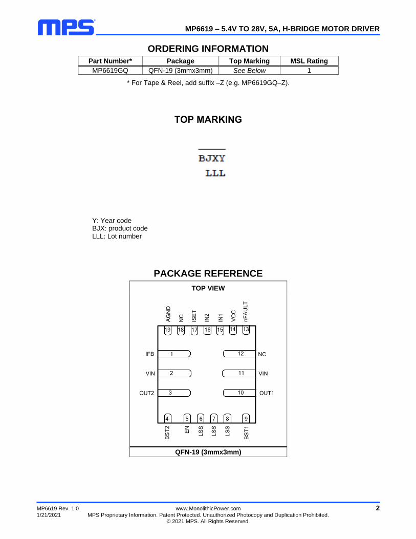
ORDERING INFORMATION
Part Number* Package Top Marking MSL Rating
MP6619GQ QFN-19 (3mmx3mm) See Below 1
* For Tape & Reel, add suffix –Z (e.g. MP6619GQ–Z).
TOP MARKING
Y: Year code BJX: product code LLL: Lot number
PACKAGE REFERENCE
TOP VIEW
151617
IN2
ISE
T
IN1
2VIN
14
VC
C
1319
AG
ND
18
NC
76 854 9
1IFB
3OUT2
11 VIN
12 NC
10 OUT1
BS
T2
EN
LS
S
LS
S
LS
S
BS
T1
nF
AU
LT
QFN-19 (3mmx3mm)

MP6619 – 5.4V TO 28V, 5A, H-BRIDGE MOTOR DRIVER
MP6619 Rev. 1.0 www.MonolithicPower.com 3
1/21/2021 MPS Proprietary Information. Patent Protected. Unauthorized Photocopy and Duplication Prohibited. © 2021 MPS. All Rights Reserved.
PIN FUNCTIONS
Pin # Name Description
1 IFB Current-sense signal feedback. Connect the IFB and LSS pins together.
2, 11 VIN Input supply.
3 OUT2 Output terminal 2.
4 BST2 Bootstrap pin for the OUT2 high-side MOSFET (HS-FET) gate driver. Connect a capacitor between the BST2 and OUT2 pins.
5 EN IC enable.
6, 7, 8 LSS Low-side source connection. For current sense, connect a current-sense resistor between the LSS pin and power ground.
9 BST1 Bootstrap pin for the OUT1 HS-FET gate driver. Connect a capacitor between BST1 and OUT1.
10 OUT1 Output terminal 1.
12, 18 NC No connection. Float this pin or connect it to AGND.
13 nFAULT Fault indication output. nFAULT is active low for fault conditions.
14 VCC 5V LDO output for internal driver and logic.
15 IN1 Output 1 control input. IN1 is pulled down internally.
16 IN2 Output 2 control input. IN2 is pulled down internally.
17 ISET Current trip voltage setting. Connect a resistor to GND from the ISET pin.
19 AGND Ground for internal logic.
ABSOLUTE MAXIMUM RATINGS (1) Supply voltage (VIN) .................................... 36V VOUTx ..................................... -0.3V to VIN + 0.3V VBST1 ................................................... VOUT1 + 6V VBST2 ................................................... VOUT2 + 6V LSS .............................................. -0.3V to +0.6V All other pins ................................... -0.3V to +6V Continuous power dissipation (TA = 25°C) (2) QFN-19 (3mmx3mm) ................................. 2.5W Junction temperature ................................ 150°C Lead temperature ..................................... 260°C Storage temperature ................ -65°C to +150°C
ESD Ratings Human body model (HBM) ........................ ±2kV Charged device model (CDM) ............. ±1.25kV
Recommended Operating Conditions (3)
Supply voltage (VIN) ......................... 5.4V to 28V Operating junction temp (TJ) .... -40°C to +125°C
Thermal Resistance (4) θJA θJC
QFN-19 (3mmx3mm) ............. 50 ....... 12 ... °C/W
Notes:
1) Exceeding these ratings may damage the device. 2) The maximum allowable power dissipation is a function of the
maximum junction temperature TJ (MAX), the junction-to-ambient thermal resistance θJA, and the ambient temperature TA. The maximum allowable continuous power dissipation at any ambient temperature is calculated by PD (MAX) = (TJ (MAX) - TA) / θJA. Exceeding the maximum allowable power dissipation can produce an excessive die temperature, which can cause the regulator to go into thermal shutdown. Internal thermal shutdown circuitry protects the device from permanent damage.
3) The device is not guaranteed to function outside of its operation conditions.
4) Measured on a JESD51-7, 4-layer PCB.

MP6619 – 5.4V TO 28V, 5A, H-BRIDGE MOTOR DRIVER
MP6619 Rev. 1.0 www.MonolithicPower.com 4
1/21/2021 MPS Proprietary Information. Patent Protected. Unauthorized Photocopy and Duplication Prohibited. © 2021 MPS. All Rights Reserved.
ELECTRICAL CHARACTERISTICS VIN = 24V, TA = 25°C, unless otherwise noted.
Note:
5) Guaranteed by design.
Parameters Symbol Condition Min Typ Max Units
Supply Voltage
VIN operating range VIN 5.4 28 V
Turn-on threshold VIN_ON VIN rising edge 5.1 5.35 V
Turn-on hysteretic voltage VIN_HY 0.3 V
IC Supply
Shutdown current IIN_SD EN = 0 1 μA
Quiescent current IIN_SBY EN = 1, no load current 1.6 2.2 mA
VCC regulator voltage VVCC 4.5 5 5.5 V
VCC regulator dropout voltage 20mA load 100 mV
Logic
Logic high threshold 1.5 V
Logic low threshold 0.4 V
IC start-up delay tDELAY EN active to switching 230 350 µs
Current Control
Current trip voltage VITRIP VITRIP = 200mV 180 200 220 mV
VITRIP = 100mV 85 100 115 mV
Off time tITRIP After ITRIP 1 ms
Power MOSFET
High-side MOSFET (HS-FET) on resistance
42 65 93 mΩ
Low-side MOSFET (LS-FET) on resistance
42 65 93 mΩ
Minimum on time 200 ns
Bootstrap for High-Side Driver
Forward voltage for BST charge 0.5 V
BST UVLO Rising edge 2 V
Protection
Over-current (OC) retry time tOCP 1 ms
OC threshold IOCP 10 A
Input over-voltage (OV) threshold VINOVP 32.2 34 35.5 V
Thermal shutdown (5) 150 °C
Thermal shutdown hysteresis(5) 20 °C
MP6619 – 5.4V TO 28V, 5A, H-BRIDGE MOTOR DRIVER
MP6619 Rev. 1.0 www.MonolithicPower.com 5
1/21/2021 MPS Proprietary Information. Patent Protected. Unauthorized Photocopy and Duplication Prohibited. © 2021 MPS. All Rights Reserved.
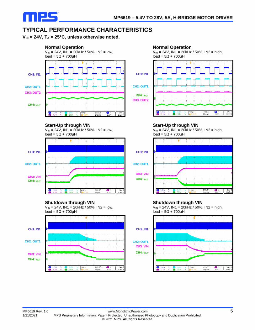
TYPICAL PERFORMANCE CHARACTERISTICS VIN = 24V, TA = 25°C, unless otherwise noted.
Normal Operation VIN = 24V, IN1 = 20kHz / 50%, IN2 = low, load = 5Ω + 700µH
Normal Operation VIN = 24V, IN1 = 20kHz / 50%, IN2 = high, load = 5Ω + 700µH
CH1: IN1
CH2: OUT1
CH3: OUT2
CH4: IOUT
CH1: IN1
CH2: OUT1
CH4: IOUT
CH3: OUT2
Start-Up through VIN VIN = 24V, IN1 = 20kHz / 50%, IN2 = low, load = 5Ω + 700µH
Start-Up through VIN VIN = 24V, IN1 = 20kHz / 50%, IN2 = high, load = 5Ω + 700µH
CH1: IN1
CH2: OUT1
CH3: VIN
CH4: IOUT
CH1: IN1
CH2: OUT1
CH3: VIN
CH4: IOUT
Shutdown through VIN VIN = 24V, IN1 = 20kHz / 50%, IN2 = low, load = 5Ω + 700µH
Shutdown through VIN VIN = 24V, IN1 = 20kHz / 50%, IN2 = high, load = 5Ω + 700µH
CH1: IN1
CH2: OUT1
CH3: VIN
CH4: IOUT
CH1: IN1
CH2: OUT1
CH3: VIN
CH4: IOUT

MP6619 – 5.4V TO 28V, 5A, H-BRIDGE MOTOR DRIVER
MP6619 Rev. 1.0 www.MonolithicPower.com 6
1/21/2021 MPS Proprietary Information. Patent Protected. Unauthorized Photocopy and Duplication Prohibited. © 2021 MPS. All Rights Reserved.
TYPICAL PERFORMANCE CHARACTERISTICS (continued) VIN = 24V, TA = 25°C, unless otherwise noted.
IC Enable VIN = 24V, IN1 = 20kHz / 50%, IN2 = low, load = 5Ω + 700µH
IC Enable VIN = 24V, IN1 = 20kHz / 50%, IN2 = high, load = 5Ω + 700µH
CH1: IN1
CH2: OUT1
CH3: EN
CH4: IOUT
CH1: IN1
CH2: OUT1
CH3: EN
CH4: IOUT
IC Disable VIN = 24V, IN1 = 20kHz / 50%, IN2 = low, load = 5Ω + 700µH
IC Disable VIN = 24V, IN1 = 20kHz/50%, IN2 = high, load = 5Ω + 700µH
CH1: IN1
CH2: OUT1
CH3: EN
CH4: IOUT
CH1: IN1
CH2: OUT1
CH3: EN
CH4: IOUT

MP6619 – 5.4V TO 28V, 5A, H-BRIDGE MOTOR DRIVER
MP6619 Rev. 1.0 www.MonolithicPower.com 7
1/21/2021 MPS Proprietary Information. Patent Protected. Unauthorized Photocopy and Duplication Prohibited. © 2021 MPS. All Rights Reserved.
FUNCTIONAL BLOCK DIAGRAM
M1
M2
M1
Driver
G1
M2
Driver
G2
M3
M4
M3
Driver
G3
M4
Driver
G4
BG&
Control
EN
LDO
VCC
ISET
G1
G3
VCC VCC
VCP VCP
OUT1
OUT2
OCP
OTP
OVP
VIN
AGND
Charge
Pump VCP
VCC VCC
BST1 BST2
LSS
IFB
Fault
Detection
Gate
Driver
Control
LogicIN2
Contr
olle
r
IN1
Curr.
Reg.
RISET
nFAULT
Current-Sense
Signal Feedback
Current Trip
Voltage Setting
G2
G4
RISEN
Figure 1: Functional Block Diagram

MP6619 – 5.4V TO 28V, 5A, H-BRIDGE MOTOR DRIVER
MP6619 Rev. 1.0 www.MonolithicPower.com 8
1/21/2021 MPS Proprietary Information. Patent Protected. Unauthorized Photocopy and Duplication Prohibited. © 2021 MPS. All Rights Reserved.
OPERATION The MP6619 is an H-bridge motor driver that operates from a supply voltage up to 28V and delivers a motor current up to 5A. Typically, the MP6619 is used to drive a brushed DC motor.
Input Logic
For the MP6619, control of each half-bridge is independent, using EN, IN1, and/or IN2 (see Table 1).
Table 1: Truth Table
EN INx OUTx
0 x Z
1 0 L
1 1 H
Shutdown Mode
If the EN signal is pulled low, the MP6619 shuts down. In shutdown mode, all circuits and blocks are disabled, and the MP6619 consumes less than 1µA of shutdown current. There is about 150ns of deglitch time on EN to avoid a mistrigger.
Current Limit
The MP6619 has a programmable current limit function. The output current flowing through both two low-side MOSFETs is sensed by an external sense resistor. If the load current reaches the current trip threshold, a current limit condition is triggered, the entire H-bridge switches to a high-impedance state with all MOSFETs turned off. After a fixed off time (tITRIP), the MOSFETs are re-enabled, and the cycle repeats.
The current limit is triggered when the IFB pin voltage (VIFB) reaches the current trip voltage (VITRIP). For example, if a 40mΩ sense resistor is connected from LSS to ground, and the current trip voltage (VITRIP) is 200mV, when the output current reaches 5A, VIFB reaches 200mV and a current trip occurs.
Current Trip Voltage Setting
The current control trip value is set by connecting a resistor between ISET and GND. When ISET is floating, the current trip voltage is set to its default (200mV). If a resistor is connected between ISET and GND, the current
trip voltage can be reduced below 200mV to reduce power loss on the sense resistor. The IC needs about 0.3ms to detect whether a resistor is available on ISET when the IC starts up for the first time. During this time, the IC is not switching. The relationship of the current trip voltage and RISET is calculated with Equation (1):
ITRIP
ISET
40V 0.2
R kΩ (1)
For example, if RISET is 80kΩ, the trip voltage is 100mV. For better accuracy, a 40kΩ to 80kΩ resistance is recommended to achieve a 200mV to 100mV current trip voltage.
Start-Up Sequence
The IC needs about 0.3ms to detect whether a resistor is available on ISET when the IC starts up for the first time. During this time, the IC is not switching.
VCC LDO Regulator
The IC employs a low-dropout (LDO) regulator to provide a constant voltage (5V) at VCC. The VCC voltage (VVCC) is used for the internal power supply of the logic circuit and driver circuit. When the input voltage drops, VVCC drops together with VIN. If VVCC drops below 4.8V, the IC triggers a power reset sequence and shuts down. The IC resumes normal operation when VVCC exceeds 5.1V.
High-Side MOSFET (HS-FET) Driver
The M1 and M3 high-side MOSFETs (HS-FETs) are N-channel MOSFETs. When M1 and M3 turn on, a bootstrap supply voltage (VBSTx) across BST1 and BST2 is required. VBSTx is generated by a combination of the internal charge pump and a 5V VCC. This allows the IC to operate at 100% duty cycle to provide enough driver voltage for the M1 and M3 HS-FETs.
Over-Current Protection (OCP)
The over-current protection (OCP) circuit limits the current through each MOSFET by reducing the gate driver voltage to the MOSFET. If the MOSFET current remains in the over-current (OC) condition (above IOCP) for longer than the OC deglitch time, all MOSFETs in the H-bridge are disabled and nFAULT is driven low.

MP6619 – 5.4V TO 28V, 5A, H-BRIDGE MOTOR DRIVER
MP6619 Rev. 1.0 www.MonolithicPower.com 9
1/21/2021 MPS Proprietary Information. Patent Protected. Unauthorized Photocopy and Duplication Prohibited. © 2021 MPS. All Rights Reserved.
The driver remains disabled for tOCP and is re-enabled automatically.
Input Over-Voltage Protection (OVP)
During operation, the energy stored in the load current is delivered to the input side during the freewheeling time. If VIN and the output current (IOUT) are high enough, the energy sent back to the input side causes VIN to rise up. To avoid IC damage due to a high voltage spike, the IC employs input voltage protection.
If voltage applied to the VIN pin is above the OVP threshold, the H-bridge output is disabled and nFAULT is driven low. This protection is released when VIN drops to a safe level.
Junction Over-Temperature Protection (OTP)
If the die temperature exceeds safe limits, all H-bridge MOSFETs are disabled and nFAULT is driven low. Once the die temperature has fallen to a safe level, normal operation resumes automatically.
Fault Indication Output (nFAULT)
The MP6619 provides an nFAULT pin that is driven active low if any of the protection circuits are activated. These fault conditions include over-current (OC), over-temperature (OT), and over-voltage (OV). nFAULT is also driven low when a current-limit trip occurs. nFAULT is an open-drain output, and requires an external pull-up resistor. Once any fault conditions are removed, nFAULT is pulled inactive high by the pull-up resistor.
Enable/Disable (EN)
To enable the MP6619, apply a logic high signal to EN, and the high-level signal time needs to be above about 10µs. Pull EN to logic low, and set the low-level signal above 100ns to shut down the IC.

MP6619 – 5.4V TO 28V, 5A, H-BRIDGE MOTOR DRIVER
MP6619 Rev. 1.0 www.MonolithicPower.com 10
1/21/2021 MPS Proprietary Information. Patent Protected. Unauthorized Photocopy and Duplication Prohibited. © 2021 MPS. All Rights Reserved.
APPLICATION INFORMATION Selecting the Input Capacitor
The input capacitor reduces the surge current drawn from the input supply and the switching noise from the device. The input capacitor impedance at the switching frequency should be less than the input source impedance to prevent the high-frequency switching current from passing through to the input. Ceramic capacitors with X5R or X7R dielectrics are recommended for their low ESR and small temperature coefficients. A higher-value capacitor is helpful for reducing input voltage ripple and noise. For most applications, two 22µF ceramic capacitors in parallel are sufficient. It is recommended to connect one capacitor to each VIN pin.
Setting the Output Current limit
If a resistor is connected between ISET and GND, the output current limit value can be calculated with Equation (2):
OUT
ISET ISEN
40 1I 0.2
R kΩ R Ω (2)
If ISET is left floating, the current limit setting formula is calculated with Equation (3):
OUT
ISEN
0.2I
R Ω (3)
For example, if RISET is 80kΩ, then the trip voltage is 100mV. For better accuracy, a 40kΩ to 80kΩ resistance is recommended to achieve a 200mV to 100mV current trip voltage.
Setting the Sense Resistor
The power loss of the sensing resistor (PLOSS_RIFB) can be calculated with Equation (4):
2
ITRIPLOSS_RIFB
ISEN
VP
R Ω (4)
To guarantee a current reference, the nominated power rating of the sensing resistor is recommended to be twice the calculated power loss with at least a 1% accuracy resistor.
PCB Layout Guidelines
Efficient PCB layout is critical for stable operation. For the best results, refer to Figure 2 on page 11 and follow the guidelines below:
1. Place the input capacitor close to VIN.
2. Use a wide copper plane for the input, output, and GND connecting wire to improve thermal performance.
3. Place as many GND vias near the output and input capacitor as possible to improve thermal performance.
4. Keep the sense resistor loop as short as possible.
5. Keep the current-sense feedback signal far away from noise sources.

MP6619 – 5.4V TO 28V, 5A, H-BRIDGE MOTOR DRIVER
MP6619 Rev. 1.0 www.MonolithicPower.com 11
1/21/2021 MPS Proprietary Information. Patent Protected. Unauthorized Photocopy and Duplication Prohibited. © 2021 MPS. All Rights Reserved.
TYPICAL APPLICATION CIRCUIT
VIN
AGND
IN1
VCCISET
IN2
OUT2
OUT1
5.4V to 28V
MP6619
C1
C2
BST1
BST2
IFB
Optional
R2
R3
R4
C4
C5
LSSnFAULT
EN M
DC
Motor
Figure 2: Typical Application Circuit
MP6619 – 5.4V TO 28V, 5A, H-BRIDGE MOTOR DRIVER
MP6619 Rev. 1.0 www.MonolithicPower.com 12
1/21/2021 MPS Proprietary Information. Patent Protected. Unauthorized Photocopy and Duplication Prohibited. © 2021 MPS. All Rights Reserved.
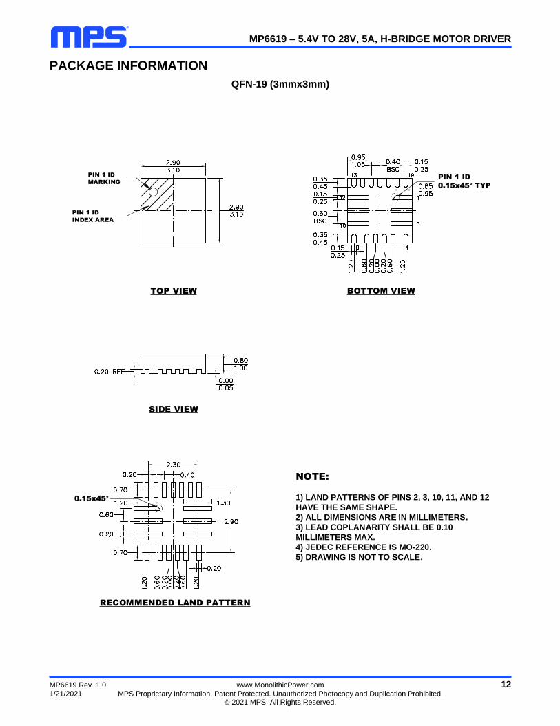
PACKAGE INFORMATION
QFN-19 (3mmx3mm)
SIDE VIEW
BOTTOM VIEW
NOTE:
1) LAND PATTERNS OF PINS 2, 3, 10, 11, AND 12
HAVE THE SAME SHAPE.
2) ALL DIMENSIONS ARE IN MILLIMETERS.
3) LEAD COPLANARITY SHALL BE 0.10
MILLIMETERS MAX.
4) JEDEC REFERENCE IS MO-220.
5) DRAWING IS NOT TO SCALE.
PIN 1 ID
MARKING
TOP VIEW
PIN 1 ID
INDEX AREA
RECOMMENDED LAND PATTERN
PIN 1 ID
0.15x45° TYP
0.15x45°

MP6619 – 5.4V TO 28V, 5A, H-BRIDGE MOTOR DRIVER
MP6619 Rev. 1.0 www.MonolithicPower.com 13
1/21/2021 MPS Proprietary Information. Patent Protected. Unauthorized Photocopy and Duplication Prohibited. © 2021 MPS. All Rights Reserved.
CARRIER INFORMATION
Pin1 1 1 1 1ABCD ABCD ABCD ABCD
Feed Direction
Part Number Package
Description Quantity/
Reel Quantity/
Tube Quantity/
Tray Reel
Diameter
Carrier Tape Width
Carrier Tape Pitch
MP6619GQ–Z QFN
(5mmx5mm) 5000 N/A N/A 13in 12mm 8mm

MP6619 – 5.4V TO 28V, 5A, H-BRIDGE MOTOR DRIVER
Notice: The information in this document is subject to change without notice. Please contact MPS for current specifications. Users should warrant and guarantee that third-party Intellectual Property rights are not infringed upon when integrating MPS products into any application. MPS will not assume any legal responsibility for any said applications.
MP6619 Rev. 1.0 www.MonolithicPower.com 14
1/21/2021 MPS Proprietary Information. Patent Protected. Unauthorized Photocopy and Duplication Prohibited. © 2021 MPS. All Rights Reserved.
REVISION HISTORY
Revision # Revision
Date Description Pages Updated
1.0 1/21/2021 Initial Release -