Embed Size (px)
Citation preview

Molecule Corrals as Templates for the Formation of Metal and Silicon
Nanostructures Jennifer D. McBride, Ben Van Tassel!, Rebecca C. Jachmann, and Thomas P. Beebe, Jr.*
Department of Chemistry
University of Utah
Salt Lake City, UT 84112
August 29, 2000 * Author to whom correspondence should be addressed:
Dr. Thomas P. Beebe, Jr. University of Delaware Department of Chemistry 175 Brown Laboratory Newark, DE 19716 Phone: (302) 831-1888 Fax: (302) 831-6335 e-mail: beebe®udel.edu
2
Abstract:
Gold and silicon nanostructures have been produced by condensing vacuum-
evaporated materials and semiconductors onto nanometer-sized etch-pit templates
preformed on the surface of highly oriented pyrolytic graphite (HOPG). Billions of
monodispersed monolayer-deep etch-pit templates, or “molecule corrals” can be
produced in a range of diameters from a few to hundreds of nanometers due to the linear
etch rate of carbon atom removal as a function of time. Evaporation and subsequent
annealing of gold and silicon has resulted in the formation of metal and semiconductor
nanostructures on the graphite basal plane. The size and shape of the nanostructures were
examined using scanning tunneling microscopy (STM), and the total coverage of the
nanostructures and other chemical properties were examined using x-ray photoelectron
spectroscopy (XPS). By varying the ratio of the total amount of material evaporated to
the diameter of the etch-pit templates, three distinct types of metal nanostructures were
observed to form on the molecule corral templates: rings, disks, and mesas. This method
of producing nanostructures is a process that is inherently parallel and allows direct
control over the final diameters and shapes (in two and three dimensions) of the
nanostructures formed.
Introduction
Nanometer-sized clusters of metallic atoms have been widely investigated due to
the size-dependent structural and electronic properties that differ from those of the bulk
metal, and from those of isolated single atoms. These nanostructures offer novel ideas
for applications in catalysis, microelectronics, sensors, biological interfaces, and

3
advanced material design. By confining or growing nanometer-sized structures,
interesting properties due to quantum confinement effects have been observed. Tailoring
these effects by controlling the island growth has generated much interest in the field of
quantum dots. 1-7
A number of methods have been developed for the production of metal
nanostructures. Several groups have employed scanning probe microscopes to deposit
various metal nanoparticles onto the highly oriented pyrolytic graphite (HOPG) basal
plane.8-16 These probe techniques offer the benefits of site-directed deposition, but
suffer from the inherent serial drawback of producing nanostructures one at a time.
Optical methods such as lithography can produce structures in a parallel fashion, however
they are limited in feature size to ~180 nm due to diffraction.17 There are also at least
three parallel processes used to generate nanoscale arrays: nanosphere lithography,17
nanochannel glass replica masking,18,19 and porous-membrane template-based
synthesis.20-23
Vacuum evaporation of metals onto HOPG has been a widely studied topic.
These previous works were carried out in order to determine the structure, aggregation,
and nucleation of metals on the graphite basal plane. Previous research8,24-27 has found
that clusters of metal atoms gather in and around defects on the surface of HOPG under
specific conditions to form metal nanostructures. Edge defects, steps or terrace edges in
the basal plane of graphite, have been observed to anchor metal nanostructures during
STM and AFM imaging. Hövel et al. capitalized on this observation, and have used
monolayer etch pits as high-density anchoring sites in the vacuum deposition of gold and
silver,28,29 in order to study the three-dimensional structure of the clusters by STM.

4
Control of molecule corral density can be accomplished actively or passively.
Active control has been accomplished by use of high-resolution ion-beam lithography in
a time-of-flight secondary ion mass spectrometer employing a Ga or Cs ion gun (the
former with nominally 60-nm spatial resolution). Exposure of the HOPG surface to
controlled doses of ions has been used to create defects. These high-defect graphite
substrates are then subjected to the oxygen etching procedure described in the
experimental section below. Ion dose density controls the overall pit density, whereas
ion energy controls the defect penetration depth and the ensuing pit depth. Active control
of patterning using ions is the subject of a forthcoming paper and will not be discussed
further.30 Passive control of etch pit density is accomplished by selecting HOPG samples
having specific, previously characterized, intrinsic defect densities. These intrinsic
defects are the starting sites for carbon etching reactions,31 and thus passive control of pit
density can be used by selecting HOPG samples with known (i.e. previously
characterized) defect densities. Unlike active control, passive control cannot be used to
control where etch pits are located on the graphite basal plane, and regular arrays are not
possible.
“Molecule corrals,” monolayer-deep etch pits which form on the basal plane of
graphite, have been used in a number of applications and investigations in our group.
They have been used to isolate ensembles of liquid crystal molecules in order to study the
nucleation rates of self assembly in various sized corrals.31-34 They have also been used
to investigate the formation and dynamics of domain boundaries in self-assembled
molecular films,35 and to study chiral “information transfer” between nearby domains of
self-assembled monolayers.34 Molecule corrals have also been used to investigate the

5
ordering of adsorbed self-assembled monolayers and the effect of tip interaction on these
self-assembled films while imaging by STM.36 In this paper, we have now combined the
vacuum evaporation of materials with “molecule corrals,” and have used them as
templates in the formation of metal and semiconductor nanostructures. By varying the
ratio of the template diameter to the amount of metal deposited, we have observed the
formation of three distinct types of nanostructures: rings, disks, and flat-topped mesas.
Experimental
Highly oriented pyrolytic graphite, ZYB grade, was generously supplied by Dr.
Arthur W. Moore of Union Carbide/Advanced Ceramics. A piece of tape-cleaved HOPG
was etched in air using a Lindberg Hevi-Duty quartz tube furnace, producing CO2 (g) and
removing C atoms. Samples were heated to 650° C inside the furnace and etched for
various times to produce monolayer-deep (3.35 Å) etch pits (typically 20 minutes etch
time to produce 700-Å-diameter templates). The etching procedure is described in
further detail elsewhere.37-39 The template structures were then imaged by STM
(typically 0.80 V – tip positive, 160 pA, 3.07 µm sec-1 tip scan rate) prior to metal
deposition in order to determine the pit density, etch-pit diameter, and pit depth. The
STM used in these studies is custom built and has been described elsewhere.40 Images
were acquired in both constant-height and constant-current (topographic) mode, using
tips mechanically cut from Pt/Ir (80:20) wire. All images were acquired at room
temperature under ambient conditions.
Etched HOPG samples containing molecule corrals were attached to a tantalum
sample holder fitted with a chromel/alumel thermocouple and placed in a commercial

6
vacuum evaporator (BOC Edwards Auto 306). Samples were resistively heated to 350°C
under vacuum with a base pressure of 2×10⁻⁶ Torr for two hours, in order to remove
surface contaminants from the freshly cleaved HOPG surface. Immediately before
material deposition, the temperature of the sample was raised to the intended annealing
temperature of 350°C or 400°C, as indicated. Varying amounts of gold from 4 to 25
monolayers (1 ML ≈ 1×10¹⁵ atoms cm-2), were deposited onto the pre-etched HOPG
samples containing molecule corrals with a deposition rate of 0.08 to 0.4 ML s-1 by
heating 99.9% gold shot (Alfa Aesar) in a tungsten boat (Edwards). The total amount of
gold deposited and the deposition rates were monitored using a quartz-crystal
microbalance (Inficon XTC/2). After deposition, the samples were annealed at 350°C
and 2×10⁻⁶ Torr for two hours. Once the annealing was complete, and the sample
temperature cooled below 100°C, the vacuum chamber was vented with high purity
nitrogen, and the samples were removed from the chamber. The samples were then
characterized by STM in air, and images were compared to those obtained prior to metal
deposition. Scanning conditions for gold-coated HOPG templates varied, but were
typically 0.60 to 0.85 V sample bias (tip positive), 70 to 100 pA tunneling current, and
1.22 to 2.04 µm sec-1 tip scan rate.
In order to use the STM tip to intentionally remove gold from the sample surface,
the scanning conditions were adjusted to 0.1 V sample bias, 1 nA tunneling current, and a
scan rate of 6.0 µm s-1. The latter experiments were necessary to examine the
relationship between nanostructure size and molecule corral template size.
Silicon wafer fragments were cleaned with methanol, then placed in 49%
hydrofluoric acid for 30 min. (CAUTION: Extreme care must be taken when

7
handling HF; please refer to MSDS for proper procedures. Use proper safety
equipment and clothing when handling). The cleaned silicon fragments were placed in
a tungsten boat and were vacuum evaporated in a manner similar to that used for gold.
Annealing temperatures were similar to those used for gold: 450° C for two hours. The
STM scanning conditions for silicon-coated HOPG templates varied, but were typically
14 mV to 0.99 V sample bias (tip positive), 50 to 80 pA tunneling current, and 1.02 µm
sec-1 tip scan rate.
HOPG samples coated with gold and silicon were also analyzed using x-ray
photoelectron spectroscopy (XPS). XPS was performed with a VG Scientific 220i-XL
instrument equipped with a monochromatic Al Kα x-ray source. Typical operating
conditions for the x-ray source were 400-µm nominal x-ray spot size (FWHM) operating
at 15 kV, 8.9 mA setting and 100 W for both survey and high-resolution spectra. A 2-
micron thick aluminum window was used to isolate the x-ray chamber from the sample
analysis chamber, in order to prevent high-energy electrons from impinging on the
sample. Survey spectra, from 0 to 1200 eV binding energy, were collected at 100-eV
pass energy with an energy resolution of ∼1 .0 eV, a dwell time of 100 ms, and a total of
two scans averaged. High-resolution spectra were collected at a pass energy of 20 eV,
energy resolution of ∼0.1 eV, dwell time of 100 ms, and a total of 7 scans averaged in the
respective binding energy ranges for C 1s (275 – 295 eV); O 1s (522 – 542 eV); Au 4f
(76 – 96 eV); and Si 2p (94 – 108 eV). The C 1s peak, centered at 284.6 eV did not
require charge shifting, therefore no charge shifting of other elemental peaks was
necessary. Peak areas were fitted using VG Eclipse software with component peaks
assigned by the authors. Quantification was performed using previously published

8
methods,41 and atomic sensitivity factors (C 1s: 1.00, O 1s: 2.93, Au 4f7/2: 9.58, Si 2p1/2:
0.28, Si 2p3/2: 0.54, and Si 2poxide: 0.82).
Results and Discussion
Flat-bottomed monolayer-deep (3.35 Å) etch pits are produced from the high-
temperature etching of HOPG in air.25,39,42 Because the diameter of the etch pits varies
linearly with the time the graphite is exposed to reaction temperature, one can directly
and conveniently control the diameter of the etch pits by varying the amount of time the
substrate is heated, as seen in Figure 1. The etch rate for these ZYB grade samples was
determined to be 30.8 ± 2.7 Å min-1 for monolayer-deep etch pits. The y-intercept of this
plot is zero within error limits (23.7 ± 43.1 Å).
Additional information about the production of monolayer and multilayer HOPG
etch pits has been reported previously by this group.37 Due to the fact that pit growth
(i.e. carbon removal) begins and ends at the same time for all of the pits, this process is
inherently parallel, and a narrow gaussian distribution of pit diameters is produced, as
seen in Figure 2. Etch pits were analyzed using scanning tunneling microscopy to gather
information about the etch pits (i.e. diameter, depth, and density of pits on the surface).
An example of these etch pits is shown in the constant-current STM image in Figure 3.
The narrow distribution of pit diameters (817 ± 86 Å in this case) is typical. The HOPG
substrates used as templates in this study had a surface pit density ranging from 3×10⁸ to
8×10⁹ pits cm-2 or 3 to 80 pits µm-2, with the majority of the samples falling at the lower
end of this range. It is interesting to note that this corresponds to an initial defect density
of 3×10⁻⁸ to 7×10⁻⁷ monolayers.

9
Gold was evaporated onto pre-characterized graphite etch-pit templates.
Following vacuum evaporation, the graphite template surface was heated to allow the
adsorbed gold to diffuse across the graphite basal plane. This results in the nucleation
and growth of gold atom islands along edges of the molecule corrals and steps on the
HOPG surface. Figures 4a and 4b depict an unusually high density of gold
nanostructures that have collected along step edges and inside etch-pit templates. We
have observed the gold structures to be fixed inside the molecule corrals, essentially
surrounded and enclosed within a circular step edge, where the monolayer-deep wall acts
as a collection site for gold nucleation and growth. As seen in Figures 4a and 4b, this
collection at step edges occurs at all step edges, including non-corral step edges. A
region with an unusually high step population was selected to illustrate this collection of
gold. A white line drawn by hand in Figure 4b indicates such a non-corral step edge
decorated with gold disk nanostructures.
Control of nanostructure shapes
By varying the ratio of the total average thickness of deposited gold to the average
etch-pit diameter, three distinct types of gold nanostructures have been observed. These
structures are gold rings, gold disks and gold mesas, as shown in Figure 5. Smaller ratios
of gold to etch-pit diameters (∼0 .02) resulted in gold diffusion and adsorption at the rims
of the monolayer-deep etch pits. This produces an array of gold-ring nanostructures. An
example structure can be seen in Figure 5a (total z-scale is approximately atomic).
Similar graphite edge decoration has been observed with silver and platinum deposited
electrochemically.8,43,44

10
As the ratio of average gold-thickness to pit-diameter increases (∼0. 04), gold
rings are added to, gradually filling in the entire corral template with gold, producing an
atomically flat circular disk having the diameter of the molecule corral on which it
formed. The filling in of the etch pits with gold is apparently due to the favorable gold
cohesive packing energy in comparison to the low gold-carbon adsorption energy on the
open HOPG terraces. An example of a partially filled gold disk structure (referred to
later as “pre-mesas”) is depicted in Figure 5b (z-dimension 40 Å). At slightly higher
annealing temperatures or longer annealing times, the six atomically flat gold island pre-
mesas shown would typically merge together to form a low-profile, flat-topped gold disk.
The fact that the inner diameters of these pre-mesas were smaller, and the outer diameters
were larger than the molecule corral templates indicates that the gold ring pre-mesa
structures are anchored on the molecule corrals. The pre-mesas essentially straddle the
monolayer-deep steps which act as collection sites for gold nucleation and growth.
With an even larger gold-thickness to template-diameter ratio (∼0. 3), the disks
begin to grow upward, and then begin to expand outward from the original etch-pit
diameter. These structures are similar to the structures produced using tip-induced
scanning probe deposition of gold and silver,8-11 although the latter must be produced
one at a time. The vertically growing disks resemble a pillar or desert mesa. The tops
appear to be nearly atomically flat with a (111) surface orientation, as evidenced by their
hexagonal structure and step intersection angles. It does not appear that the gold mesas
adopt the same epitaxial relationship, if any, with the underlying HOPG, since hexagon
edges from different hexagons are not always parallel, as also seen by Hövel et al..29 We
have grown mesas with heights varying from 20 to 100 Å. An example of a gold-mesa

11
structure is shown in Figure 5c. The line scan across the tops of these nanostructures,
Figure 5d, shows that the left and right mesas are 44 Å and 38 Å high respectively, and
atomically flat except for some adsorbed gold atoms on top. The etch pits on which these
mesas formed were ∼140 Å in diameter.
While most structures were formed on pieces of graphite with a lower density of
pit templates than that shown in Figure 4, we wanted to see if it was also possible to form
nanostructures on substrates of higher pit-density without completely coating the graphite
with a thin layer of gold. The following analysis focused on forming mesa structures.
Deposition of 25 ML of gold and annealing at a temperature of 530° C for two hours
resulted in nanostructures evenly distributed on molecule corrals on the surface of the
graphite template. Figure 6 shows the gold mesa structures formed on this etch-pit
template. As expected a high density of mesa structures has collected along a step edge
running diagonally through the image, highlighted by the two arrows. Prior to gold
deposition, the density of etch pits was determined to be (8.2 ± 0.5)×109 pits cm-2, and the
diameter of these pits was 194 ± 49 Å. After gold deposition, the density of the gold
nanostructures was found to be (1.04 ± 0.20)×1010 pits cm-2, 1.3 ± 0.2 times that of the
etch-pit templates, essentially equivalent within error limits. The diameters of the mesas
were 429 ± 73 Å, 2.2 ± 0.3 times larger than the molecule corral templates on which they
are located. This indicates that the gold mesas straddle the monolayer-deep steps, similar
to the pre-mesa growth, supporting the hypothesis that the pre-mesas gradually fill in to
form the flat-topped mesa nanostructures.
In addition to hexagonal nanostructures, many triangular gold mesa
nanostructures have also formed on this high-pit-density graphite template. This provides
12
additional evidence for the formation of well-ordered, crystalline gold nanostructures.
This transition from hexagonal to triangular nanostructure shapes has been a widely
studied topic in two-dimensional metal-on-metal growth.45-47 From the evidence shown
in the STM images of gold nanostructures, it would appear that the equilibrium
hexagonal shape of the nanostructures45 is the predominant crystalline structure.
However, the presence of non-equilibrium triangular nanostructures suggests a
temperature-dependent effect. The effect of annealing temperature on nanostructure
shape and size will be further investigated for this system.
XPS analysis of three separate spots on a gold-coated HOPG template (24 ML
gold deposited) indicates approximately 10.1 ± 3.7% surface coverage with gold, as
shown by the survey scan in Figure 7. Oxygen was also present on these samples (∼2%)
primarily due to adsorption of oxygen onto the graphite surface.
Silicon nanostructures were formed by vacuum evaporation of 60 Å of silicon
onto 120-Å-diameter molecule corrals on the HOPG basal plane. The samples were
annealed at 450°C in a vacuum of 2×10⁻⁶ Torr for two hours prior to STM analysis.
Immediately following deposition, the samples were transferred through air to be
analyzed by XPS, as shown in Figure 8. Oxygen is present on the graphite as a result of
both the etching process and surface adsorption (also seen in Figure 7 for gold).
Therefore, although oxygen was present with silicon in a ∼2: 1 atomic ratio, a direct 2:1
ratio of oxygen to SiOx can not be assumed since some oxygen is associated directly with
the carbon. It was found that the silicon nanostructures consist of both the oxidized and
metallic forms of silicon, as shown in the high-resolution Si 2p XPS spectra of Figure 9.
The peak-fitted data displays a 6.3 ratio of metallic to oxidized silicon, indicating that the

13
majority of the silicon in the nanostructures exists in the metallic form. Given the
vacuum pressure and transfer through air, it is expected that the silicon would form an
oxide layer, either during evaporation or immediately following evaporation.
These samples were then analyzed by STM and found to contain silicon
nanostructures centered on molecule-corral templates, shown in Figure 10. It can be seen
from this figure that the silicon nanostructures consist of a layered terrace structure.
Pixel height histograms values of four silicon mesa areas, outlined in black (A-D), have
been plotted and are shown in Figure 11 (region A in Figure 10 corresponds to plot 11a,
etc.). Typically, cursor line profiles or line scans between two points have been used to
analyze the topographic information contained in STM images. For such a line scan, the
number of data points analyzed depends on the number of pixels in the image. In
addition, the random error in a line scan must be estimated from the standard deviation of
data obtained from many different line scans, or by estimating the random noise in a
single line scan. However, by plotting a histogram of height values for each pixel within
a defined region, we increased the number of data points analyzed by a factor of 10
(Figures 11b and 11d) to 24 (Figure 11a). This histogram approach clearly takes
advantage of the large amount of information contained within an STM image, is more
robust to noise, and is superior to a single cursor profile.
In order to bin the data properly, slope correction must be performed on the small
area of interest in order to level the area independently in both in the x and y directions.
This was performed using a first-order slope compensation function applied on a HOPG
terrace area near the nanostructure in question, and selected by the authors. The
histograms of the four silicon nanostructure regions (Figure 11) have been analyzed by

14
fitting the data with multiple (two to four) gaussian peaks in order to determine the peak
center values and error. These silicon terraces are, on average, 4.7 ± 0.1 Å high. The
interplanar spacing of the silicon (111) terraces have been determined previously to be
3.1 Å.48 It has also been shown that the silicon (100) surface displays a bilayer domain
reconstruction where the surface periodicities are (2×1) and (1×2) alternating, with
terrace heights of 1.36 Å49,50. Further analysis of the layering behavior of these
nanostructures is planned in order to determine the orientation of these terrace layers.
Atomic resolution was not possible on the Si terraces, probably due to the oxide layer.51
Nanostructure heights and diameters
Gold ring nanostructures begin at low gold coverages as single-atom rings (see
Fig. 5a), and grow with increasing gold coverage to eventually be made up of individual
“pre-mesa” structures in a circular pattern surrounding the etch-pit templates. Each
corral contains between five and eight individual pre-mesa structures. The heights and
diameters of these individual pre-mesa gold nanostructures were compared to the heights
and diameters of a separate HOPG template sample containing “final” mesa (i.e. not pre-
mesas) nanostructures. Analysis of these two HOPG template samples resulted in the
distributions shown in Figure 12. Pre-mesa gold-ring structures have heights of 111 ± 30
Å, and diameters of 329 ± 78 Å, while final gold mesa nanostructures have heights of
116 ± 35 Å, and diameters of 429 ± 73 Å. This indicates that regardless of the total
amount of gold deposited (8.5 ML for pre-mesa gold rings and 25 ML for final gold
mesas), the annealing temperature (450° C for pre-mesa rings, 530° C for final gold
mesas), or the diameter of the etch pits (818 ± 86 Å for pre-mesa rings, 193 ± 49 Å for

15
final gold mesas), there exists an optimal height of ∼11 4 ± 46 Å for gold nanostructures
regardless of the nanostructure diameter. Therefore, any additional gold results in
horizontal expansion of the nanostructures, causing pre-mesa gold rings to gradually fill
in, and final gold mesas to expand beyond the diameter of the original etch-pit templates.
Gold Nanostructure mobility
During STM imaging of the gold nanostructures, it was found that some of the
nanostructures could be removed by the STM tip as it was scanned across the HOPG
surface. This removal of metal structures was also observed by others.15,29,52 In
agreement with those observations which in general were not made on corral-based
nanostructures, the sweeping away of the gold structures occurs primarily to
nanostructures that do not have an anchoring etch pit or a step edge beneath them, or are
incomplete pre-mesa gold ring structures with hollow centers. By varying the STM
imaging conditions (decreasing the bias, increasing the tunneling current, and increasing
the scan rate) we were able to remove gold from the underlying etch pits. It was this
ability to remove discs and mesas that allowed us to compare corral template diameters to
nanostructure diameters accurately. Figures 13a and 13b depict the same two etch-pit
templates decorated with pre-mesa gold-ring structures. Figure 13b shows that gold
contained within the molecule corral templates has migrated slightly (top arrow) due to
tip-induced movement while obtaining the image for Fig. 8a. The gold on the lower pit
has been removed or pushed to the center of the etch pit, as shown by the bottom arrow.
Figures 13c and 13d show line scans of the pre-mesa gold ring nanostructures and of the
monolayer-deep etch pit. As discussed above, pre-mesa gold ring structures are made up

16
of individual gold mesas. Line A shows the flat-topped, vertical-walled structure similar
to that seen for final gold mesas (Fig. 5d). The molecule corral template is also apparent
in this line scan, since the center of the ring structure (between the two gold-ring pre-
mesas) is 3.35 Å lower than the HOPG basal plane on either side of the two mesa
structures. Line B is a typical line scan of a 3.35-Å monolayer-deep molecule corral.
Conclusions
Gold and silicon nanostructures have been produced by condensing vacuum
evaporated materials onto nanometer-sized etch-pit templates preformed on the surface of
HOPG. Monolayer-deep etch-pit templates or “molecule corrals” can be produced in a
range of diameters from a few to hundreds of nanometers due to the linear etch rate of
carbon atom removal as a function of etch time. Evaporation and subsequent annealing
of varying amounts of gold onto these molecule corral templates has resulted in the
formation of metal nanostructures. It was found that by varying the ratio of the total
amount of metal evaporated to the diameter of the etch-pit templates, three distinct types
of nanostructures, rings, disks, and mesas, were observed to form. Smaller ratios of gold-
thickness to etch-pit diameters (0.02) resulted in gold diffusion and adsorption at the rims
of the monolayer-deep etch pits, producing arrays of gold-ring nanostructures. At a
slightly higher ratio (0.04) the small gold rings are added to, and gradually fill in the
entire corral template with gold, producing an atomically flat circular disk. With an even
larger gold-thickness to template-diameter ratio (0.3), the disks begin to grow upward,
and then begin to expand outward from the original etch-pit perimeter.
17
The tops of the gold nanostructures appear to be nearly atomically flat with a
(111) surface orientation, as evidenced by their hexagonal structure. Further evidence of
the formation of gold nanocrystals is the production of triangular nanostructures. It does
not appear that each gold mesa adopts the same epitaxial relationship, if any, with the
underlying HOPG, since hexagonal and triangular edges from different hexagons are not
always parallel or quantized in multiples of 60 degrees.
Regardless of the total amount of gold deposited, the temperature of annealing, or
the diameter of the molecule corral templates, it appears that there exists an optimal
maximum height ( ∼114 Å) for gold nanostructures. Any additional evaporation of gold
results in horizontal expansion of the structures, causing gold rings to fill in and mesas to
expand beyond the diameter of the original etch-pit templates.
Tip-induced movement of nanostructures proved a problematic issue for imaging
silver nanostructures. However, the ability to remove gold discs and mesas allowed an
accurate comparison of the diameters of the corral templates and resulting nanostructures.
This tip-induced mobility also helped to confirm that gold nanostructures are centered
over the graphite etch-pit templates.
Silicon nanostructures were also formed by vacuum evaporation of silicon onto
HOPG etch-pit templates. These nanostructures were found to consist of both the
oxidized and metallic forms of silicon, either as a result of silicon oxidation during
evaporation, or due to formation of a thin oxide film encapsulating the nanostructures. It
was found that the silicon mesas formed multilayered, terrace structures. Scanning
tunneling spectroscopy is planned to further investigate the electronic properties of
multilayered silicon nanostructures.

18
Acknowledgments
This work was supported by the National Science Foundation (CHE-9814477), IPMI
Student Award for Precious Metal Research (JDM), and the Alfred P. Sloan Foundation.
TPB acknowledges John T. Yates, Jr., to whom this volume is dedicated, and who served
as the author’s graduate advisor, for his mentoring and friendship.
References
(1) Weisbuch, C.; Binter, B. Quantum Semiconductor Structures; Academic Press:
New York, 1991.
(2) Banyai, L.; Koch, S. W. Semiconductor Quantum Dots; World Scientific:
Singapore, 1993.
(3) Alivisiatos, A. P. Science 1996, 271, 933.
(4) Leonard, D.; Medeiros-Ribeiro, G.; Drexler, H.; Pond, K.; Hansen, W.; Kotthaus, J.
P.; Petroff, P. M. Inst. Phys. Conf. Ser 1995, 141, 819.
(5) Adams, J. A.; Wang, J. N.; Beton, P. H.; Henini, M. NATO ASI Ser., Ser. E 1993,
239, 191.
(6) Olejniczak, W.; Klusek, Z.; Kobierski, P.; Belogolovskii, M. Solid State Commun.
1995, 95, 295.
(7) Samuelson, L.; Carlsson, N.; Castrillo, P.; Gustafsson, A.; Hessman, D.; Lindahl, J.;
Montelius, l.; Petersson, A.; Pistol, M.-E.; Seifert, W. Jpn. J. Appl. Phys., Part 1
1995, 34, 4392.
(8) Li, W.; Virtanen, J. A.; Penner, R. M. Applied Physics Letters 1992, 60, 1181.

19
(9) Wawro, A.; Kasuya, A.; Czajka, R.; Horiguchi, N.; Nishina, Y. Surf. Coat. Technol.
1994, 67, 173.
(10) Li, W.; Virtanen, J. A.; Penner, R. M. J. Phys. Chem. 1994, 98, 11751.
(11) Song, J. Q.; Li, C. Z.; He, H. X.; Chen, Y.; Wang, L.; Liu, Z. F. Mol. Cryst. Liq.
Cryst. 1997, 294, 51.
(12) Rohrer, H. Microelectron. Eng. 1995, 27, 3.
(13) Poetzschke, R. T.; Gervasi, C. A.; Vinzelberg, S.; Staikov, G.; Lorenz, W. J.
Electrochim. Acta 1995, 40, 1469.
(14) Hendricks, S. A.; Kim, Y.; Bard, A. J. J. Electrochem. Soc. 1992, 139, 2818.
(15) Zoval, J. V.; Stiger, R. M.; Biernacki, P. R.; Penner, R. M. J. Phys. Chem. 1996,
100, 837.
(16) Binns, C.; Bayliss, S. C. Surface Science 1989, 214, 165.
(17) Hulteen, J. C.; Van Duyne, R. P. J. Vac. Sci. Technol. A. 1995, 13, 1553.
(18) Nguyen, P. P.; Pearson, D. H.; Tonucci, R. J.; Babcock, K. J. Electrochem. Soc.
1998, 145, 247.
(19) Pearson, D. H.; Tonucci, R. J.; Bussmann, K. "Arrays of submicron metal rings
fabricated using NCG replica masks," Naval Research Laboratory, 1997.
(20) Brumlik, C. J.; Menon, V. P.; Martin, C. R. J. Mater. Res. 1994, 9, 1174.
(21) Martin, C. R. Acc. Chem. Res. 1995, 28, 61.
(22) Martin, C. R. Chem. Mater. 1996, 8, 1739.
(23) Hulteen, J. C.; Martin, C. R. J. Mater. Chem. 1997, 7, 1075.
(24) Hennig, G. R. J. Chem. Phys. 1964, 40, 2877.
(25) Chu, X.; Schmidt, L. D. Surface Science 1992, 268, 325.

20
(26) Ahn, Y.-O.; Seidl, M. Journal of Applied Physics 1995, 77, 5558.
(27) Hammiche, A.; Webb, R. P.; Wilson, I. H. J. Vac. Sci. Technol., B 1994, 12, 1413.
(28) Hövel, H.; Becker, T.; Bettac, A.; Reihl, B.; Tschudy, M.; Williams, E. J. J. Appl.
Phys. 1997, 81, 154.
(29) Hövel, H.; Becker, T.; Bettac, A.; Reihl, B.; Tschudy, M.; Williams, E. J. Appl.
Surf. Sci. 1997, 115, 124.
(30) Zhu, Y. J.; McBride, J. D.; Hansen, T. A.; Beebe, T. P., Jr. to be submitted. .
(31) Patrick, D. L.; Cee, V. J.; Beebe Jr., T. P. Science 1994, 265, 231.
(32) Patrick, D. L.; Beebe, T. P., Jr. Langmuir 1994, 10, 298.
(33) Patrick, D. L.; Cee, V. J.; Beebe, T. P., Jr. J. Phys. Chem. 1996, 100, 8478.
(34) Patrick, D. L.; Cee, V. J.; Morse, M. D.; Beebe, T. P., Jr. J. Phys. Chem. B 1999,
103, 8328.
(35) Patrick, D. L.; Cee, V. J.; Purcell, T. J.; Beebe, T. P., Jr. Langmuir 1996, 12, 1830.
(36) Stevens, F.; Buehner, D.; Beebe, T. P., Jr. J. Phys. Chem. B 1997, 101, 6491.
(37) Stevens, F.; Beebe, T. P., Jr. J. Phys. Chem. B. 1998, 102, 10799.
(38) Stevens, F.; Beebe, T. P., Jr. Comput. Chem. 1999, 23, 174.
(39) Chang, H.; Bard, A. J. J. Am. Chem. Soc. 1990, 112, 4598.
(40) Zeglinski, D. M.; Ogletree, D. F.; Beebe, T. P., Jr.; Hwang, R. Q.; Somorjai, G. A.;
Salmeron, M. B. Review of Scientific Instruments 1990, 61, 3769.
(41) Seah, M. P. Quantification of AES and XPS; Second ed.; Seah, M. P., Ed.; John
Wiley & Sons: New York, 1990; Vol. Volume 1: Auger and X-ray Photoelectron
Spectroscopy, pp 657.
(42) Chu, X.; Schmidt, L. D. Carbon 1991, 29, 1251.
21
(43) Zoval, J. V.; Lee, J.; Gorer, S.; Penner, R. M. J. Phys. Chem. B 1998, 102, 1166.
(44) Li, W.; Hsiao, G. S.; Harris, D.; Nyffenegger, R. M.; Virtanen, J. A.; Penner, R. M.
J. Phys. Chem. 1996, 100, 20103.
(45) Michely, T.; Comsa, G. Two-Dimensional Island Shapes; Michely, T.; Comsa, G.,
Ed.; World Scientific: Singapore, 1998; Vol. 14, pp 498.
(46) Barabasi, A.; Stanley, H. E. Fractal Concepts in Surface Growth; Cambridge
University Press: Cambridge, 1995.
(47) Michely, T.; Hohage, M.; Bott, M.; Comsa, G. Phys. Rev. Lett. 1993, 70, 3943.
(48) Suzuki, M.; Kudoh, Y.; Homma, Y.; Kaneko, R. Appl. Phys. Lett. 1991, 58, 2225.
(49) Alerhand, O. L.; Berker, A. N.; Joannopoulos, J. D.; Vanderbilt, D. Phys. Rev. Lett.
1990, 64, 2406.
(50) Chadi, D. J. Phys. Rev. Lett. 1987, 59, 1691.
(51) In addition, an exciting continuation of this project is to examine the individual
silicon nanostructure mesas using scanning tunneling spectroscopy (STS).
Differences in the I-V plots of multilayered terrace structures as compared to
single-layer terrace structures will be examined, as will a comparison between the
STS of both silicon nanostructures and similarly sized metal nanostructures.
(52) Stabel, A.; Eichhorst-Gerner, K.; Rabe, J. P.; Gonzalez-Elipe, A. R. Langmuir
1998, 14, 7324.

22
Figure captions
Figure 1. Plot of pit diameter vs. etch time for monolayer-deep pits produced at 650° C.
One standard deviation for each data point is shown as error bars. The etch rate of 30.8 Å
min-1 is in agreement with previously published results.37
Figure 2. Histogram of typical etch-pit template diameters produced on ZYB-grade
HOPG. Solid line shown is a gaussian distribution centered at 607 Å. Mean diameter of
pits on this sample was 607 Å with a standard deviation of 53 Å (∼9% ). The number of
pits analyzed was 244.
Figure 3. 1.00-µm2 constant-height image of monolayer-deep etch-pit templates. Image
acquired with a sample bias of -0.60 V, tunneling current of 160 pA and scan rate of 6.08
µm sec-1. Notice the narrow distribution of pit diameters. This image depicts typical pit
densities used for nanostructure production (ca. 1×10⁹ pits µm-2).
Figure 4. (a) 1.00-µm2 constant-current image of gold ring nanostructures (typical
scanning conditions). The gold has collected along a step edge, as well as along three
circular etch pit edges. These etch-pit templates are ∼75 0 Å in diameter. (b) 1.00-µm2
constant-height image (-0.60 V, 170 pA, 1.22 µm sec-1 scan rate). Gold collection along
a terrace edge has been identified with a hand-drawn white line. Many circular etch pits,
some of which are merged etch-pit templates, are decorated with gold nanostructures.
These images are typical of pre-mesa gold-ring nanostructures.
Figure 5. Constant-current topographic STM images depicting the types of
nanostructures formed on etch-pit templates. (a) 0.1-µm2 image of a small gold ring
structure. Ratio of thickness of gold deposited to pit diameter was 0.02. Etch-pit
template is ∼550 Å diameter. This image was taken with a –0.99 V sample bias and 75

23
pA tunneling current. Total z-dimension is atomic in scale. (b) 0.15-µm2 area of a large
pre-mesa gold-ring structure. The etch-pit template is ∼65 0 Å diameter, and the ratio of
gold deposited to pit diameter was 0.03. This image was taken with a sample bias of –
0.60 V, tunneling current of 154 pA and scan rate of 1.22 µm sec-1. Z-dimension
corresponds to 67 Å maximum (top right structure) and –3.35 Å minimum (center of etch
pit). The outer diameter of this pre-mesa nanostructure is approximately 1100 Å.
(c) Same scanning conditions as in (b), a 0.15-µm2 area of two hexagonal gold mesas.
(d) Line scan across the tops of the two mesa structures from left to right. The heights of
these two mesas are 44 Å and 38 Å, and they are 363 Å and 500 Å in diameter. The
mesas are atomically flat except for some adsorbed gold atoms on the tops of the
nanostructures. The ratio of deposited gold thickness to pit diameter was 0.2.
Figure 6. Constant-current STM image of gold-mesa structures (typical scanning
conditions) formed on a high density (8.2×10⁹ pits cm-2) etch-pit template. After gold
deposition, the density of the gold nanostructures was found to be 1.04×10¹⁰ pits cm-2,
∼ 1.3 times that of the etch-pit templates. A high density of mesa structures has collected
along a step edge running diagonally through the image, as highlighted by the two arrows
outside the image field of view. Notice the formation of numerous triangular gold-mesa
structures.
Figure 7. XPS survey spectrum of core-level photoelectron emission from HOPG etch
pit template coated with 49 Å of gold. Oxygen is incorporated into the graphite surface
as part of the etching process and is present in the spectrum without gold (data not
shown).

24
Figure 8. XPS survey spectrum of core-level photoelectron emission from HOPG etch
pit template coated with 60 Å of silicon. Oxygen is incorporated into the graphite surface
as part of the etching process, as well as due to the formation of a silicon oxide layer
either during deposition, or immediately following deposition. Annealing temperature
was 450°C.
Figure 9. High-resolution XPS silicon 2p core-level photoelectron spectra of an etch-pit
template substrate coated with 60 Å of vacuum-deposited silicon. The solid line is the
raw data overlayed with the sum of the fitted peaks. The higher binding energy peak
(103.3 eV) corresponds to silicon oxide (2p1/2 and 2p3/2 combined). The peak separation
between the metallic Si 2p1/2 and Si 2p3/2 is 0.6 eV. The ratio of metallic silicon to
oxidized silicon was 6.3 (the sum of the 2p3/2 and 2p1/2 normalized areas of the metallic
silicon peaks and the total normalized area of the silicon oxide peak).
Figure 10. Constant-current image (0.25 µm2) of silicon mesa structures formed on etch-
pit templates (120-Å diameter). Individual nanostructures comprised of monolayer and
multilayered terraces have been identified. Terraces are, on average, 4.7 ± 0.1 Å high,
and range from 170 to 510 Å in diameter.
Figure 11. Histogram plot of height information of the rectangular regions shown in
Figure 10 (A-D). These histograms have been analyzed by fitting the data with multiple
(two to four) gaussian peaks in order to determine the peak center values and error. Prior
to binning, image data were slope corrected by a standard first-order tilt correction
algorithm and smoothed with a 9-point Savitsky-Golay smoothing algorithm, to remove
noise spikes and increase peak definition. These silicon terraces are, on average, 4.7 ±

25
0.1 Å high. The number of data points analyzed for each histogram were: 12,065 (a),
5,913 (b), 6,715 (c), and 5,925 (d).
Figure 12. Histogram of heights and diameters of pre-mesa gold ring and “final” gold
mesa nanostructures. Each pre-mesa ring structure consists of between five and eight
individual pre-mesa structures. The heights and diameters of these individual pre-mesa
gold nanostructures were compared to the heights and diameters of a separate HOPG
template sample containing “final” gold mesa nanostructures. Analysis of these two
HOPG template samples resulted in the distributions shown above. Both pre-mesa rings
and final gold mesas have approximately the same heights. This indicates that there
exists an optimal height of ∼1 12 ± 31 Å for gold nanostructures. The number of analyzed
nanostructures forming pre-mesa gold rings was 476, and the number of final gold mesa
structures analyzed was 104.
Figure 13. Tip-induced movement of pre-mesa gold ring nanostructures inside
monolayer-deep etch-pit templates a) constant-current mode; b) constant-height mode.
Two scan cycles have occurred between the image a) and image b). The gold on the
lower pit has been pushed to the center of the etch pit, as shown by the bottom arrow. In
addition, gold has been moved slightly towards the center of the top etch pit as shown by
the top arrow. Image c) depicts the beginning of atomically flat pre-mesa gold ring
structures as seen in “Line A” from image a). Part d) depicts a typical monolayer-deep
etch-pit template with a diameter of 1009 Å “Line B” in image a).

Figure 1.doc
0 5 10 15 20 250
100
200
300
400
500
600
700
800
900
Growth of HOPG Etch Pits at 650°C
Monolayer Pit Etch Rate= 30.8 ± 2.7 Å min-1
Pit D
iam
eter
(Å)
Etch Time (min)

Figure 2.doc
300 400 500 600 700 800 9000
10
20
30
40
50
60
tetch = 20 min.
Tetch = 650 °CMean Diameter
607 Å ± 9%
Histogram of Pit Diameters for HOPG TemplatesNu
mbe
r of E
tch
Pits
Pit Diameter (Å)

Figure 3.doc
Monolayer-Deep Etch Pits on HOPGPrior to Gold Deposition

Figure 4.doc
Decoration of Etch-Pit Edges with Gold Nanostructures

Figure 5.doc
Gold Rings, Disks, and Mesason HOPG Molecule Corrals

Figure 5d.doc
0 200 400 600 800 1000 1200 14000
10
20
30
40
50Atomically Flat
Gold (111)
Line Scan of Gold Mesas Formed on HOPGHe
ight
(Å)
Distance (Å)

Figure 6.doc
Gold Mesas Produced on aHigh-Pit-Density HOPG Template

Figure 7.doc
Peak Center(eV)
FWHM(eV)
Atomic%
O1s 531.9 2.37 2.0C1s 284.6 0.55 87.9
Au 4f5/2 87.8 0.66 ---Au 4f7/2 84.2 0.68 10.1
1200 1000 800 600 400 200 00
100
200
300
400
500
O A
uger
Au 4f7/2
Au 4f5/2
Au 4
d 5/2
Au 4
d 3/2
Au 4
p 3/2
Au 4
s
O 1
s
XPS of Gold Vapor Deposited onto HOPGMolecule Corrals
C 1
s
Au 4
p 1/2
Inte
nsity
(kCP
S)
Binding Energy (eV)

Peak Center(eV)
FWHM(eV)
Atomic%
O1s 532.5 1.71 6.7C1s 284.6 0.56 83.7SiOx
Si 2p1/Si 2p3/
1200 1000
100
200
300
400
C 1s
Si 2
sSi
2p
XPS of Silicon Vapor Deposited onto HOPGMolecule Corrals
Inte
nsity
(kCP
S)
103.2 1.80 3.02 100.1 0.75 ---2 99.5 0.66 6.6O A
uger O
1s
Figure 8.doc
0 800 600 400 200 0Binding Energy (eV)

Figure 9.doc
108 106 104 102 100 98 960
1
2
3
4
5
6
Si° : SiOx = 6.3
Si 2p
High-Resolution XPS of Silicon Vapor Depositedonto HOPG Molecule Corrals
Si 2p1/2
Si 2p3/2
SiOxInte
nsity
(kCP
S)
Binding Energy (eV)

Figure 10.doc
Silicon Nanostructures Formed byVacuum Evaporation onto HOPG
Molecule Corrals

Figure 11.doc
a) b)
c) d)
Histograms of Silicon Nanostructure Heights
0.0 .00.0
0.2
0.4
0.6
0.8
1.0
eight 0.1 Å
Coun
ts (N
orm
aliz
ed)
Heig0.0 5.0 10.00.0
0.2
0.4
0.6
0.8
1.0
ht= 4.6 ± 0.1 Å
Mean Height= 4.9 ± 0.1 Å
Coun
ts (N
orm
aliz
ed)
Height (Å)
0.00.00.2
0.4
0.6
0.81.0
1.21.4
Mean Height.1 Å
Coun
ts (N
orm
aliz
ed)
Heig0.0 5.0 10.0 15.00.0
0.2
0.4
0.6
0.8
1.0
1.2
Mean Height= 5.1 ± 0.3 Å
Mean Height= 4.4 ± 0.2 Å
Mean Height= 4.4 ± 0.1 Å
Coun
ts (N
orm
aliz
ed)
Height (Å)
5
Mean H= 4.8 ±
ht (Å)
5.0
= 5.0 ± 0
ht (Å)
Mean Heig
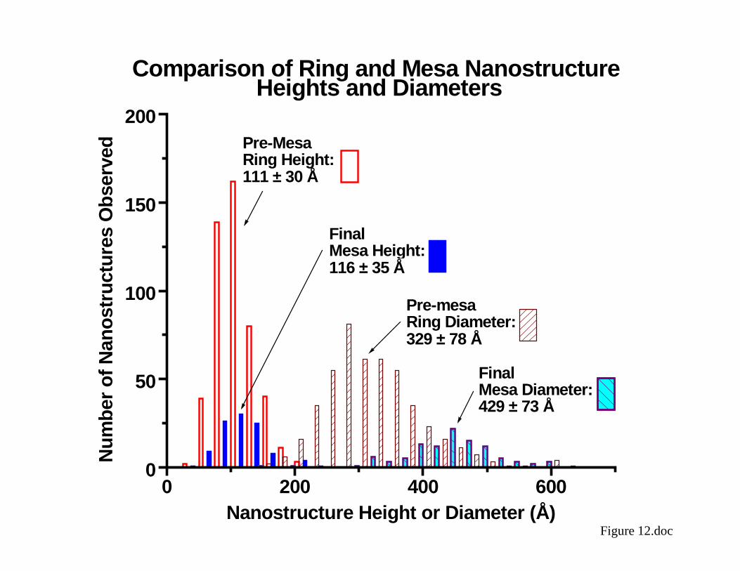
Figure 12.doc
0 200 400 6000
50
100
150
200
Comparison of Ring and Mesa Nanostructure Heights and Diameters
FinalMesa Diameter:429 ± 73 Å
FinalMesa Height:116 ± 35 Å
Pre-mesaRing Diameter:329 ± 78 Å
Pre-MesaRing Height:111 ± 30 Å
Num
ber o
f Nan
ostru
ctur
es O
bser
ved
Nanostructure Height or Diameter (Å)

Figure 13.doc
a) b)
c) d)
Tip-Induced Movement of Gold Nanostructures
0 500 1000 2000
0
1
2
3
4
5Line B
Hei
ght (
Å)
Distance (Å0 500 1000 1500 2000
01020304050607080
Monolayer-deepetch-pit
Line A
Heig
ht (Å
)
Distance (Å)
15003.4 Å
)