Embed Size (px)
Citation preview

Rev D, July 2000
July, 2000
1
AN9012
Induction Heating System Topology Review
Discrete Application Power Device DivisionFairchild Semiconductor
1. IntroductionAll IH (induction heating) applied systems are developed using electromagnetic induction whichwas first discovered by Michael Faraday in 1831. Electromagnetic induction refers to the phenom-enon by which electric current is generated in a closed circuit by the fluctuation of current inanother circuit placed next to it. The basic principle of induction heating, which is an applied formof Faraday’s discovery, is the fact that AC current flowing through a circuit affects the magneticmovement of a secondary circuit located near it. The fluctuation of current inside the primary circuitprovided the answer as to how the mysterious current is generated in the neighboring secondarycircuit. Faraday’s discovery led to the development of electric motors, generators, transformers,and wireless communications devices. Its application, however, has not been flawless. Heat loss,which occurs during the induction heating process, was a major headache undermining the overallfunctionality of a system. Researchers sought to minimize heat loss by laminating the magneticframes placed inside the motor or transformer. Faraday’s Law was followed by a series of moreadvanced discoveries such as Lentz’s Law. This law explains the fact that inductive current flowsinverse to the direction of changes in induction magnetic movement.
Heat loss, occurring in the process of electromagnetic induction, could be turned into productiveheat energy in an electric heating system by applying this law. Many industries have benefitedfrom this new breakthrough by implementing induction heating for furnacing, quenching, and weld-ing. In these applications, induction heating has made it easier to set the heating parameters with-out the need of an additional external power source. This substantially reduces heat loss whilemaintaining a more convenient working environment. Absence of any physical contact to heatingdevices precludes unpleasant electrical accidents. High energy density is achieved by generatingsufficient heat energy within a relatively short period of time.
The demand for better quality, safe and less energy consuming products is rising. Products usingIH include electronic rice cookers and pans. Safe, efficient and quick heating appliances attractmore customers. This document describes induction heating, power systems, and IH applications.

2
Rev D, July 2000
2. Types of Electric Process HeatingPrior to describing induction heating, some types of electric process heating are explained below tohelp you understand normally used heat sources.
The types of electric heating are as follows:
• Resistance Heating• Conduction Heating• Infrared Radiation Heating• Induction Heating• Dielectric Hysteresis Heating• Electric Arc Heating• Plasma Heating• Electron Beam Heating• Laser Heating
Resistance heating is the most common type of electric process heating. It uses the relationshipbetween the voltage and current of resistance in Joule’s Law.
Conduction heating exploits the heat energy generated when an object is placed between twoelectric poles, which is another application of Joule’s Law. In this case, however, a different rela-tionship exists between voltage and current, especially when the circuit current is high, becausethe object itself contains both resistance and inductance features.
The main topic of this document is induction heating, which is a combination of electromagneticinduction, the skin effect, and the principle of heat transfer. In short, induction heating refers to thegeneration of heat energy by the current and eddy current created on the surface of a conductiveobject (according to Faraday’s Law and the skin effect) when it is placed in the magnetic field,formed around a coil, where the AC current flows through (Ampere’s Law). Detailed descriptions ofinduction heating are presented in the following sections of the document.
3. Basics of Induction HeatingInduction heating is comprised of three basic factors: electromagnetic induction, the skin effect,and heat transfer. The fundamental theory of IH, however, is similar to that of a transformer. Elec-tromagnetic induction and the skin effect are described in this section. Figure 3-1 illustrates a verybasic system, consisting of inductive heating coils and current, to explain electromagnetic induc-tion and the skin effect. Figure 3-1-a shows the simplest form of a transformer, where the second-ary current is in direct proportion to the primary current according to the turn ratio. The primary andsecondary losses are caused by the resistance of windings and the link coefficient between thetwo circuits is 1. Magnetic current leakage is ignored here.

3
Rev D, July 2000
When the coil of the secondary is turned only once and short-circuited, there is a substantial heatloss due to the increased load current (secondary current). This is demonstrated in Figure 3-1-b.Figure 3-1-c shows a system where the energy supplied from the source is of the same amount asthe combined loss of the primary and secondary. In these figures, the inductive coil of the primaryhas many turns while the secondary is turned only once and short-circuited. The inductive heatingcoil and the load are insulated from each other by a small aperture. The next phase of the skineffect occurring under high frequency is presented in Section 3-2.
As the primary purpose of induction heating is to maximize the heat energy generated in the sec-ondary, the aperture of the inductive heating coil is designed to be as small as possible and thesecondary is made with a substance featuring low resistance and high permeability. Nonferrousmetals undermine energy efficiency because of their properties of high resistance and low perme-ability.
Figure 3-1: Basics of Induction Heating
3-1. Electromagnetic Induction
As shown in Figure 3-1, when the AC current enters a coil, a magnetic field is formed around thecoil according to Ampere’s Law.
N1 N2
I1 I2=I1 (N1/N2)
RL
<figure 3-1a > equivalent circuit of transformer
<figure 3-1b> secondary short
N1
I1
1
I2=I1 N1
ZL
coil current
induction current
doload secondary
coilprimary alternating
magnetic flux
H ld∫ Ni F= =
∅ µ HA=(Formula 3-1)

4
Rev D, July 2000
An object put into the magnetic field causes a change in the velocity of the magnetic movement.The density of the magnetic field wanes as the object gets closer to the center from the surface.According to Faraday’s Law, the current generated on the surface of a conductive object has aninverse relationship with the current on the inducting circuit as described in Formula 3-2. The cur-rent on the surface of the object generates an eddy current.
As a result, the electric energy caused by the induced current and eddy current is converted toheat energy as shown in Formula 3-3.
Here, resistance is determined by the resistivity (ρ) and permeability (µ) of the conductive object.Current is determined by the intensity of the magnetic field. Heat energy is in an inverse relation-ship with skin depth which is described in Section 3-2.
If an object has conductive properties like iron, additional heat energy is generated due to mag-netic hysteresis. The amount of heat energy created by hysteresis is in proportion to the size of thehysteresis. In this document, this additional energy is ignored because it is far smaller (less than10%) than the energy generated by induction current.
3-2. Skin Effect
The higher the frequency of the current administered to the coil, the more intensive is the inducedcurrent flowing around the surface of the load. The density of the induced current diminishes whenflowing closer to the center as shown in Formula 3-4 and 3-5 below. This is called the skin effect orkelvin effect. From this effect, one can easily infer that the heat energy converted from electricenergy is concentrated on the skin depth (surface of the object).
where, ix: distance from the skin (surface) of the object, current density at x.
Io: current density on skin depth (x=0)
do: a constant determined by the frequency (current penetration depth or skin depth)
where, ρ: resistivity
µ: permeability of the object
ω: Frequency of the current flowing through the object
E dλdt------ N
d∅dt--------= = (Formula 3-2)
P E2 R⁄ i2= = R (Formula 3-3)
ix ioe x do⁄–= (Formula 3-4)
do2ρµω-------= (Formula 3-5)

5
Rev D, July 2000
Formula 3-5 states that the skin thickness is determined by the resistivity, permeability, and fre-quency of the object. Figure 3-2 below is the distribution chart of current density in relation to skinthickness.
Figure 3-2: Distribution Chart of Current Density and Skin Thickness
4. Topology Of Power SystemGenerally, semiconductor switching devices operate in Hard Switch Mode in various types of PWM DC-DC converters and DC-AC inverter topology employed in a power system. In this mode, a specificcurrent is turned on or off at a specific level of voltage whenever switching occurs, as shown in Fig-ure 4-1. This process results in switching loss. The higher the frequency the more the switchingloss, which obstructs efforts to raise the frequency. Switching loss can be calculated in a simpleway as shown in Formula 4-1 below. Switching also causes an EMI problem, because a largeamount of di/dt and dv/dt is generated in the process.
where, Psw : switching loss [W]
Vsw : switching voltage [V]
Isw : switching current [A]
fs : switching frequency [kHz]
ton : switch turn-on time [s]
toff : switch turn-off time [s]
x0
io
do
currentdensity
PSW12---VSWISWfS ton toff+( )= (Formula 4-1)

6
Rev D, July 2000
Figure 4-1: Wave Form of a Switching Device
By raising the switching frequency, you can reduce the size of a transformer and filter, which helpsbuild a smaller and lighter converter with high power density. But as presented earlier, switchingloss undermines the efficiency of the entire power system in converting energy, as more losses aregenerated at a higher frequency. Switching loss can be partly avoided by connecting a simplesnubber circuit parallel to the switching circuit. However, the total amount of switching loss gener-ated in the system remains the same. The loss avoided, has in fact, just moved to the snubber cir-cuit.
Higher energy conversion efficiency at high frequency switching can be obtained by manipulatingthe voltage or current at the moment of switching to become zero. This is called “Soft Switching”,which can be subcategorized into two methods: Zero-voltage switching and Zero-current switch-ing. Zero-voltage switching refers to eliminating the turn-on switching loss by having the voltage ofthe switching circuit set to zero right before the circuit is turned on. Zero-current switching is toavoid the turn-off switching loss by allowing no current to flow through the circuit right before turn-ing it off. The voltage or current administered to the switching circuit can be made zero by using theresonance created by an L-C resonant circuit. This topology is named a “resonant converter.”
In Zero-current switching, the existing inductance is absorbed into the resonant circuit, eliminatingthe surge in voltage in a turn-off situation. A voltage surge resulting from an electric discharge ofjunction capacitance, which occurs upon turning on the switching circuit, cannot be avoided. Thismethod has a defect of causing switching loss (0.5CV2f). Zero-voltage switching, however, is freefrom such a defect by making both the existing inductance and capacitance to be absorbed by theresonant circuit. This eliminates any chance of causing a surge in current both at turn-off (causedby inductance) or turn-on (by capacitance) conditions. Zero-voltage switching enables switchingwith less loss while substantially reducing the problem of EMI at high frequency. This difference infeatures make Zero-voltage switching more desirable than Zero-current switching.
PSW(on)leakage lossconduction loss PSW(off)
0
0
0
Turn-on Turn-off Turn-onSwitchcontrol
ISW
VSW
conduction voltageleakage
toff ton

7
Rev D, July 2000
As a resonant converter provides most of the energy conversion efficiency in a power system byminimizing switching loss, it is widely used in a variety of industries. And this is also the reason whythe converter is adopted in the Induction Heating Power System Topology, which is described indetail in this document. Power systems for home appliances, e.g. electronic rice cookers, andother kinds of cookers, generally employ a ZVS (Zero-voltage switching) resonant converter, whichcan be further classified into two major types: a half-bridge series resonant converter and a quasi-resonant converter. These types of topology are studied in detail in section 5 of this document.
Resonant Converter
The resonant circuit of a resonant converter consists of a capacitor, an inductor, and resistance.Two types of resonant converters are generally used: a series resonant circuit and a parallel reso-nant circuit.
Figure 4-2 shows these two common types. When power is connected, electric energy as shown inFormula 4-3 is stored in the inductor and transferred to the capacitor. Formula 4-4 simplifies thecalculation of the amount of energy stored in the capacitor to be sent to the inductor. Resonanceoccurs while the inductor and the capacitor exchange the energy. The total amount of energystored in the circuit during resonance remains unchanged. This total amount is the same as theamount of energy stored at peak in the conductor or capacitor.
As some energy is lost due to resistance in the resonance process, the total amount of energy storedin the inductor decrements in each resonant exchange. The resonance frequency, which is the speedof energy transfer, is determined by capacitance (C) and inductance (L) as shown in Formula 4-9.
i 2I sin ωt A[ ]= (Formula 4-1)
(Formula 4-2)VC1C---- i td∫ 2I
ωC--------- ωt V[ ]cos–= =
EL12---Li2 LI2 ωt J[ ]sin2== (Formula 4-3)
EC12---CVC
2 I2
ω2C-----------= ωtcos2 LI2 ωtcos2 J[ ]== (Formula 4-4)
EL EC+ LI2 sin2( ωt cos2ωt ) LI2 I2
ω2C----------- J[ ]==
(Formula 4-5)

8
Rev D, July 2000
The inductive reactance and the capacitive reactance are summarized in Formula 4-6, and 4-7,respectively. The size of impedance in a series resonant circuit is determined as shown in Formula 4-8.
Figure 4-2: Resonant Circuit
At the resonance frequency, the inductive reactance of Formula 4-6 and the capacitive reactanceof Formula 4-7 become the same, i.e. the voltage of the power source and the current in the circuitstay at the same level. The resonance frequency can be summarized as shown in Formula 4-9. Thecurrent in the circuit reaches its peak when the source frequency becomes identical to the resonance fre-quency. It decrements when the source frequency gets higher or lower than the resonance frequency.
The properties of reactance in a circuit are called special impedance, which can be described asshown in the following Formula 4-10.
And the selection ratio of a half-bridge series resonant circuit is as shown in the following Formula4-11.
Rv
+vr
iL C
(a) Series resonant
Gi
(b) Parallel resonant
L C
XL jωL j2πfL Ω[ ]= = (Formula 4-6)
XC1
jωC----------
1j2πfC--------------- Ω[ ]= = (Formula 4-7)
Z R2 ωL 1
ωC--------–
2+ Ω[ ]= (Formula 4-8)
2πfL1
2πfC------------- fo
1
2π LC------------------- Hz[ ]=⇒= (Formula 4-9)
ZO XL XC ωOL 1ωOC------------ L
C----= = = = =
(Formula 4-10)XO
2XL XC
LC----=×=
QωOL
R----------- 1
ωoCR----------------
Zo
R------= = = (Formula 4-11)

9
Rev D, July 2000
As shown in the formula above, the smaller the resistance is than the inductance, i.e. when thesource frequency gets closer to the resonance frequency, the sharper the frequency curve of Fig-ure 4-3 and the bigger the value of Q. The numerator is the energy accumulated in the inductorduring resonance and the denominator is the average amount of energy consumed in resistance ineach cycle. The frequency curve below demonstrates the relationship between current/outputenergy and source frequency when the source voltage of the resonant circuit is set at equal. Thecurrent and output energy reaches its maximum value at resonance frequency.
In the area where the switching frequency is lower than the resonance frequency, the inductivereactance has a direct relationship with the switching frequency. In other words, the lower the fre-quency, the smaller the inductive reactance. And according to Formula 4-7, the capacitive reac-tance is in inverse relationship with the frequency. As the reactance becomes more capacitive, thecurrent gets higher than the voltage in status. When the switching frequency increases (in Formula4-8), impedance gets bigger, enlarging the amount of output energy as shown in Figure 4-3. In theopposite situation, a lower switching frequency leads to a smaller impedance, causing the outputenergy to decrement.
In the area where the switching frequency is higher than the resonance frequency, the higher theswitching frequency, the bigger the inductive reactance. Here, the value of the capacitive reac-tance becomes smaller according to Formula 4-7. The higher inductive reactance causes the cur-rent to be lower than the voltage in status. In this situation, a higher switching frequency isaccompanied by an increase of impedance (Formula 4-8), causing the output energy to be lower (asshown in Figure 4-3). When the switching frequency goes down, the impedance is decreased, rais-ing the output energy (as in Formula 4-8).
Figure 4-3: Frequency Curve
5. Induction Heating Application SystemsAdvanced technology in developing semiconductor chips switching at a high frequency has madeit possible to introduce new switching devices with sophisticated functions in a smaller size at alower price. The induction heating system, once dominant only in some specific areas like guidedmissiles, has opened a new phase in developing highly efficient electronic home appliances, e.g.rice cookers and other kinds of cookers. This section presents the operating theory of an IH ricecooker, a power systems as a whole, and more detailed description of the controlling circuit in apower system.
outputcurrent
capacitive inductive
source frequencyfo

10
Rev D, July 2000
5-1. Operating Theory of an IH Rice Cooker
The concept of induction heating, employed in the application of an IH rice cooker, was alreadyexplained in section 3. This concept can be simplified as follows. First, convert the AC current com-ing from the power source to DC using a rectifier. Then, connect this DC current to a high fre-quency switching circuit to administer high frequency current to the heating coil. According toAmpere’s Law, a high frequency magnetic field is created around the heated coil. If a conductiveobject, e.g. the container of a rice cooker is put inside the magnetic field, then induced voltage andan eddy current are created on the skin depth of the container as a result of the skin effect andFaraday’s Law. This generates heat energy on the surface of the container. Rice is cooked byusing this heat energy.
Figure 5-1: Operating Theory of IH Rice Cooker
5-2. Power System of an IH Rice Cooker
There are two types of topology used in a power system as mentioned in section 4: a half-bridgeseries resonant converter and a quasi-resonant converter. These two topologies have their ownmerits and demerits. The merits of a half-bridge series resonant converter are: stable switching,low cost, and a streamlined design. As the voltage of the circuit is limited to the level of the inputvoltage, the switching circuit can have low internal pressure, which helps reduce the cost. Thedesign of the switching control component, inside a circuit, can be streamlined. There are alsosome demerits. As the half-bridge method requires two switching circuits, the overall working pro-cess becomes more complicated and the size of the heat sink and PCB should also be larger. Inaddition, the gate operating circuits must be insulated.
One of the merits of a quasi-resonant converter is that it needs only one switching circuit inside.This enables a relatively smaller design for the heat sink and PCB, making the working process farsimpler. Another strong point is the fact that the system ground can be shared. A quasi-resonantconverter is not free from defects. Most of all, switching is relatively unstable. And high internalpressure of the switching circuit, caused by the resonant voltage administered to both sides of thecircuit, pushes the cost of the circuit higher. Besides, the design for the controlling component ismore complicated. But as mentioned earlier, technological improvements in high frequency semi-conductor switching devices has lead to innovation in terms of low price, high performance, and
powersource
rectifier
highfrequencyinverter
working coil
load
heat
AC from the power source high frequency AC high frequency magnetic field
DC

11
Rev D, July 2000
reliability. Quasi-resonant converters are now generally used because of the smaller heat sink andPCB size and a simpler operating process. The following describes the operation of a half-bridgeseries resonant converter and a quasi-resonant converter.
5-2-1. Half-bridge Series Resonant Converter
A variety of design methods are available for a power system using a half-bridge series resonantconverter. Figure 5-2 is a block diagram of a power system in a very simplified form in which reli-ability and economy are factored in. This system is comprised of an AC power supply, main powercircuit, control circuit, input current detection circuit, resonant current detection circuit, and gateoperation circuit. All the necessary procedures for designing and testing the system are shown inthe block diagram. The drawing below does not contain the heater and cooling fan. The operationof a power system as a whole is illustrated in the following figure.
Figure 5-2: Power System Using Half-bridge Series Resonant Converter
The AC (220V/60Hz) power passes through the rectifier to be transmitted to the capacitor. Capaci-tors in existing power systems are too small in capacity to do the leveling work leading to the cre-ation of rectified current in 120Hz, which is not the proper level for DC operation. The system for anIH rice cooker, however, does not require a big capacitor to make DC more leveled, as the primarypurpose of the system is to generate heat energy. Rather, the rugged form of DC helps improve thepower factor of the system. In this system, the leveling capacitor serves as a filter preventing thehigh frequency current from flowing toward the inverter and from entering the input part. Input cur-rent becomes the average of the inverter current, and the ripples flow to the leveling capacitor.
The voltage passing the leveling capacitor is turned into a square wave in the process of high fre-quency switching in the inverter. The high frequency harmonics contained in the square wave areeliminated by the Lr, Cr filter. The square wave enables resonance in the resonant circuit, which inturn, creates a magnetic field around the resonant inductor affecting the load (rice container). Eddycurrents are formed around the surface of the object, generating heat energy.
Main Power Circuit
input currentdetection
controlcircuit
MCOMGate Drive Circuit
SGH40N60UFD
resonantcurrent detection
LoadSGH40N60UFD
load
MICOMgate drive circuit

12
Rev D, July 2000
The input current flowing, through the AC input section, to the rectifier and the resonant currentflowing through the inverter to the resonant circuit are input to the control circuit. In order to controlthe maximum level of input and resonant current, the control circuit sets the switching frequency ofthe inverter, administering it to the gate of the inverter switch via the gate operating circuit.
Micom allows the detection circuit to examine the input current to determine the presence of a con-ductive object, protecting the system by manipulating the on/off status of the control circuit. Moredetailed descriptions of each part are presented below.
1) Main Power Circuit
The main power circuit employs a half-bridge series converter switching at a high frequency asshown in Figure 5-3. The switching circuit consists of an IGBT (Insulated Gate Bipolar Transistor,SGH40N60UFD). Zero voltage/current turn-on switching is enabled by turning on the IGBT whilethe diode is in turn on period. The resonant circuit comprises of resonant inductance (Lr) and reso-nant capacitance (Cr). The capacitors, C1 and C2, are the lossless turn-off snubbers for theswitches, S1 and S2.
Figure 5-3: Main Power Circuit
A circuit equivalent to a resonant circuit is described in Figure 5-4. The load in circuit (a) is equiva-lent to the circuit in (b) where the transformer has resistance connected to the secondary circuit.And this can be simplified as in the circuit (c), where R*, L*, and Cr are directly connected. R* in (c)indicates the resistance of the primary circuit of the transformer converted from the secondary. L*means the inductor on the primary side of the transformer (Lr), which is a resonant inductor com-bining the leakage inductor and the secondary inductor.
According to the actual measurement of the system L*=52.7uH and Cr=0.8uF, which leads to thefollowing formula of resonance frequency, f0.
Vdc
AC input
rectifier
inverter
resonant tank
load
S1D1 C1
D2 C1S2
LrCr
(Formula 5-1)fo1
2π LC------------------- 24.5 kHz[ ]= =

13
Rev D, July 2000
With regard to the switching frequency explained in section 4, the inductive area has more advan-tages than the capacitive area in many aspects (see reference number 18 for more information).Hence, the switching frequency of the system is set at 28kHz, which is higher than the resonancefrequency, in order to avoid noise generated within the audio frequency band.
Figure 5-4: Equivalents of the Resonant Circuit
Operation Theory
By connecting the IGBT switching circuit, S1 and S2 in parallel to diodes D1 and D2, current loss isminimized. When S1 is turned-off, D2 helps S2 stay on zero voltage/current before being turnedon, thereby substantially reducing current loss (the same is the case with S1). There is no reverse-recovery problem as the voltage on both sides remains zero after the diode is turned off. However,as the switching circuit is turned off at around the upper limit of voltage and current, some switch-ing loss results on turn-off. The capacitors C1 and C2, acting as turn-off snubbers connected inparallel to S1 and S2, keep this loss to a minimum. Upon turn-on the switching circuit starts fromzero voltage/current, so these turn-off snubbers operate as lossless turn-off snubbers.
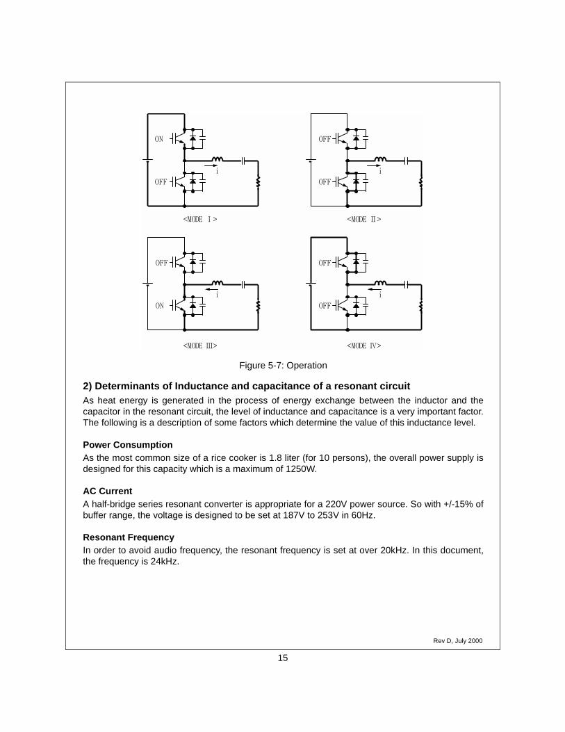
The configuration of a half-bridge series resonant converter (Figure 5-3) can be simplified as anequivalent circuit illustrated in Figure 5-5. Figure 5-6 is a wave form of a frequency cycle in eachpart of the main power circuit. Turn on S1, when the current of the L*-Cr resonant circuit flows inthe opposite direction through D1 (S1 and S2 remain off). Until t<t0, the resonant current flows inthe opposite direction through D1, rather than passing directly through S1. The following Figure 5-7 describes the resonance in each mode (I-IV).
Figure 5-5: Equivalent of the Main Power Circuit
( a ) ( b ) ( c )
load
LrCr
Lr
Cr
R
L*
R*
Cr
R*
CrL*D1S1
D2S2
C1
C2
Ai +Vc -
Vdc

14
Rev D, July 2000
Figure 5-6: Wave Form of the Main Power Circuit
MODE I: t0-t1
The resonant current flowing in an inverse direction changes its direction at the point of t=t0 flowingthrough S1. In this mode the DC-LINK voltage of Vdc lets the resonant circuit accumulate energyby supplying power through S1.
MODE II: t1-t2
When S1 is turned off at the point of t=t1, the resonant current flowing through S1 begins free-wheeling through the D2 diode. In this process, a small amount of switching turn-off loss occurs asthe S1 switch is turned off while retaining some values in voltage and current. For the followingmode, S2 is turned on when t1<t<t2. As the S2 switch remains at zero voltage/current, no switch-ing loss takes place at turn-on. And the reverse-recovery of D1 does not necessarily have to befast.
After turning off S1, the resonant current passes for a short period through the snubber C1 beforefreewheeling to D2. A detailed description of this period is not presented in this document.
MODE III: t2-t3
Right after t=t2, the current freely resonates and flows in an inverse direction through S2 which isalready turned on. Here, the resonant capacitor, Cr, serves as a source of voltage.
MODE IV: t3-t4
When S2 is turned off at t=t3, the resonant current flowing through S2 starts freewheeling throughthe D1 diode. In this process, a small amount of switching loss occurs at turn-off. For the followingmode, the S1 switch is turned on at a certain point (t3<t<t4). At this point, there is no switching lossat turn-on as the S1 switch remains at zero voltage/current. And the reverse recovery of D2 doesnot have to be fast. In this mode, the energy of the resonant circuit is converted to Vdc passing D1.The operating mode after t>t4 cycles from mode I to mode IV again as described above.
Also in this process, the resonant current passes through the snubber C2 for a short period of timebefore freewheeling to D1. This period is not explained in this document.
t0 t1 t2 t3 t4
VA Vc
i
0t
15
Rev D, July 2000
Figure 5-7: Operation
2) Determinants of Inductance and capacitance of a resonant circuit
As heat energy is generated in the process of energy exchange between the inductor and thecapacitor in the resonant circuit, the level of inductance and capacitance is a very important factor.The following is a description of some factors which determine the value of this inductance level.
Power Consumption
As the most common size of a rice cooker is 1.8 liter (for 10 persons), the overall power supply isdesigned for this capacity which is a maximum of 1250W.
AC Current
A half-bridge series resonant converter is appropriate for a 220V power source. So with +/-15% ofbuffer range, the voltage is designed to be set at 187V to 253V in 60Hz.
Resonant Frequency
In order to avoid audio frequency, the resonant frequency is set at over 20kHz. In this document,the frequency is 24kHz.
i i
i i
<MODE Ⅰ> <MODE Ⅱ>
<MODE Ⅲ> <MODE Ⅳ>
ON
OFF
OFF
OFF
OFF
OFF
OFF
ON

16
Rev D, July 2000
C (capacitance)
The computation of the amount of resonant current is as follows. Here, as the input current is theaverage of the resonant current, the input current of a cycle is computed as (resonant current/2π).
The capacitance of a resonant capacitor is determined as follows:
In this document, the standard value of capacitance is 0.8 [µF].
L (Inductance)
The inductance of the resonant inductor is computed by using the capacitance as explained aboveand in Formula 4-7.
It is important to consider whether a coil, having a value of L above, is fit for the container. Thevalue of L is determined by the thickness of the coil, and the number of turns and errors.
Figure 5-8: Common Type of Main Power Circuit
3) Actual Main Power Circuit
Figure 5-8 illustrates a main power circuit, which is used more commonly than the one in Figure 5-3.The resonant capacitor, Cr, is divided into two identical capacitors, Cr1 and Cr2 (Cr1=Cr2). By hav-ing two equal capacitors, the amount of current flowing through each capacitor is reduced to halfwhile the voltage to the capacitors remains the same. This results in less heat generation causedby ESR, and the RMS value of the ripple current in the DC-LINK capacitor is also reduced to
I 2πPV
----------- 2π 1250×187 2×-------------------------- 29.7 A[ ]= = =
C I2πfV------------- 29.7
2π 24000 187 2××------------------------------------------------------ 0.74 µF[ ]= = =
L 12πf( )2C
--------------------- 1
2π 24000×( )2 0.8 106–××
---------------------------------------------------------------------- 55 µH[ ]= = =
Cr2Lr
Cr1
Vdc
1 2( )⁄

17
Rev D, July 2000
As the total amount of resonant current flowing through the inductor is equal in both systems, theamount of heat energy generated is likewise. The amount of current in a capacitor, however,shows a difference. The flow chart of the current is not provided in this document.
5-2-2. Quasi-resonant Converter
There are a number of design methods for a power system employing a quasi-resonant converter.The following Figure 5-9 features a block diagram of such a system in a streamlined form. Thissystem was actually tested. The description of the heater is omitted in this document. The SMPS isthe block that supplies power to the DC cooling fan and the control circuit. It is designed using aBUCK converter. A detailed explanation about SMPS is not provided here.
Figure 5-9: Power System Using a Quasi-resonant Converter
The total system block comprises of a main power circuit, input current detection circuit, control cir-cuit, and SMPS circuit as shown in Figure 5-9. The basic operating concept of a quasi-resonant cir-cuit is similar to that of a half-bridge series resonant converter in that heat energy is generated.However, the methods of controlling the gate in the switching circuit are totally different. Majorfunctions of each block are as follows.
1) Main power circuit
The main power circuit features a quasi-resonant converter as in Figure 5-10. This consists of theIGBT (Insulated Gate Bipolar Transistor, SGL60N90D) and a diode connected to it in parallel. Thecircuit executes high frequency switching. By turning on the IGBT while the diode is in turn-onstate, it is possible to do a turn-on switching with the voltage and current remaining at zero. Theresonant circuit is composed of resonant inductance (Lr) and resonant capacitance (Cr).
input currentdetection
SMPS control
load
LrCr
VceVdc
Main Circuit
D1S1
MCOM
SGL60N90D
resonanttank
MICOM
InputCurrentDetection
ResonantTank

18
Rev D, July 2000
Figure 5-10: Main Power Circuit
The Equivalent of a Resonant Circuit
Figure 5-11 shows the equivalent of a resonant circuit. The resistance in circuit (b) is equivalent tothe load in circuit (a). These two circuits can be remodeled in a simpler form as circuit (c), whichconsists of R*, L*, and Cr. R* is equivalent to R of transformer (b). L* is the resonant inductor com-bining Lr of the primary circuit, the leakage inductor, and the secondary inductor.
Figure 5-11: The Equivalent of a Resonant Circuit
Operating Concept
Figure 5-12 illustrates an equivalent of the main power circuit. When D1, connected to the S1switching circuit, is in turn-on state, zero voltage turn-on switching is available as Vce of the circuitbecomes zero. In this circuit, the switch must endure high internal pressure to accommodate thehigh voltage of Vce administered to both ends of the switch.
Figure 5-13 shows the wave forms of each block of the main power circuit in a cycle. Initially, S1 isturned off by the control circuit when the current flowing through L* and S1 reaches its peak. At thispoint, Vc (0)=0V. There are four modes available, as shown in Figure 5-14.
load
CrLr
VceVdc
ac input
rectifier dc
resonanttank D1
S1
LrCr
Vdc
Lr
R
CrVdc Cr
L*R*
Vdc
(a) (b) (c)

19
Rev D, July 2000
Figure 5-12: Equivalent of a Main Power Circuit Figure 5-13: Wave Forms of the Main Power Circuit
Cr
Vce
i
VgeD1
S1
L*R*
Vdc
t0 t1 t5
t
t
t
0
0
i
Vge
Vce
0
Vdc
t6t2 t3 t4
Figure 5-14: Operation
<MODE Ⅰ>
VceL*
Vdc Cr
R*
i
<MODE Ⅱ>
VceL*
Vdc Cr
R*
i
<MODE Ⅲ>
VceL*
Vdc Cr
R*
i
D1
<MODE Ⅳ>
VceL*
Vdc Cr
R*
i
S1

20
Rev D, July 2000
MODE I: t0-t1
As mentioned earlier, the switching circuit is turned off when the resonant current flowing throughthe circuit is at its peak, i.e. at t0. In this process, a turn-off switching loss occurs. The Vce level israpidly increased by the capacitor (Cr) to become DC-LINK (Vdc) at t1.
Even when the switch is turned off at t0, the current keeps incrementing to reach its peak at t1,when Vce becomes equal to Vdc, as DC-LINK is higher than the resonant voltage. At this point, theenergy stored in the inductor begins to be transferred to the capacitor.
MODE II: t1-t4
As Vdc is lower than Vce after t1, the current decreases to zero at t2, when the resonant voltagereaches its maximum. This is also the point where the transfer of the energy stored in the inductorto the capacitor is completed. The peak level of the resonant voltage has a direct relationship withthe turn-on time of the switch (MODE IV: t5-t6).
After t2, the capacitor starts discharging the energy to the inductor, which causes the voltage andthe current flowing in inverse to decrement and reach its minimum level at t3, i.e. Vce=Vdc,respectively. Passing t3, the resonant current increases as Vce<Vdc and the discharge is com-pleted at t4.
MODE III: t4-t5
After t4, the energy sent by the capacitor and stored in the inductor, is converted to DC-LINK as theD1 diode is forward biased. The resonant current is flowing through D1 during the time S1 is turned on.
MODE IV: t5-t6
As the switching circuit remains turned on while the current is freewheeling through D1, the currentflows in the right direction through the circuit and the inductor starts to store the energy, whichmakes it possible to do a zero voltage turn-on switching.
At t6, the switching circuit is turned off, returning to MODE I. As the peak level of the voltage is indirect relationship with the on-duty frequency, one can manipulate this level, i.e. output energy, byadding or reducing the on-duty frequency.
Note that the wave form of the resonant voltage changes whenever DC-LINK becomes low orthere is any change in load impedance. As explained earlier in the description of half-bridge seriesresonant converters, the bandwidth of DC-LINK (Vdc) ranges from zero to maximum as the capac-itor has a small capacity. The wave forms of the resonant voltage can be divided into three typesas shown in Figure 5-15.
Figure 5-15: Wave Forms of Resonant Voltage
t0
Vce
Vdc
Vcex2Vcex1A B C

21
Rev D, July 2000
In this figure A, B, C, and D are the waveforms of the voltage at early turn-on, normal loading, lightloading, and late turn-on situation, respectively. If the waveform of C is generated under normal cir-cumstances, it means that the value of the inductor or the capacitor is not properly set. When thewaveform of A or D appears in a normal situation, the turn-off time of the switching frequencyshould be adjusted.
While the switching circuit is on, the amount of energy stored in the inductor must be large enough.Otherwise, resonance takes place in a light loading condition. In this situation the resonant voltagehas a finite value (Vcex2) other than zero, eliminating the freewheeling period of MODE III (t4-t5)and therefore disabling a zero voltage turn-on. The following amount of energy stored in the capac-itor is lost as a result of turning on the circuit:
The quality factor (Q) of the resonant circuit must be properly maintained to keep the maximumlevel of energy stored in the inductor or capacitor as high as possible. If Q is too large, it is harderto generate heat energy. And this has a lot to do with the material used in making the container ofthe cooker. The following computation summarizes the explanation above:
= energy stored in L/ energy consumed by load in each cycle
Figure 5-16: Wave Forms At a Non-zero Voltage Turn-On
2) Main Power Circuit
The main power circuit shown in Figure 5-17 is used more than the one in Figure 5-12. By relocat-ing the capacitor as in Figure 5-17, the voltage administered to the capacitor can be substantiallyreduced, which results in a lower internal voltage inside the capacitor. As the amount of the currentflowing to the inductor is the same in both systems, the heat energy generated in the load is alsothe same. However, the current flowing to the capacitor or DC-LINK is not the same in the two dif-ferent main power circuits. This current is not illustrated in this document.
W12---CrV
2cex2fs=
t
t
t
0
0
Vge
Vce
i
0
Vdc
Vcex2
Q ωLR
------- ωLi2
Ri2--------= =

22
Rev D, July 2000
Figure 5-17: Main Power Circuit
5-3. IH Cooker
The basic operating concept and structure of the power system of an IH cooker are similar to thoseof an IH rice cooker except for the load. The load resistance of an IH rice cooker is always thesame as there is only one kind of load used (the rice container). In this case, even in times of fre-quency fluctuation, the inductance and the capacitance remain stable due to a narrow variationrange. This leads to a simple design of the control circuit as described earlier. An IH cooker, how-ever, has a different operating environment, as different kinds of vessels are loaded on the cooker,depending on the customer’s needs. This variance of load requires the turn-off time of frequency tobe changed accordingly. This is important consideration in designing the system for an IH cooker.Otherwise, the switching circuit will be damaged due to excessive switching loss which occurs dur-ing resonance similar to A and D in Figure 5-15.
Figure 5-18 is a basic form of a control system designed to meet the requirement explained above.Illustrations of other systems are not presented in this document as they are quite similar to that ofIH rice cookers.
Lr
Cr

23
Rev D, July 2000
Figure 5-18: Power System for IH Cookers Using a Quasi-resonant Converter
The control system above is designed to keep the level of output energy stable by controlling theupper limit of the voltage. A picture of a circuit employing individual circuits is provided to clearlydescribe it.
Given below is a further description of the control system.
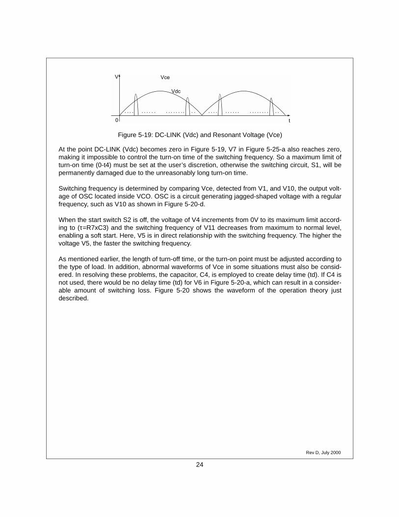
The wave forms of the resonant voltage and DC-LINK are shown in Figure 5-19. The frequency ofthe DC-LINK wave form is 120Hz, which is far smaller than the switching frequency (about 27kHz).The peak voltage level is varied depending on the size of the DC-LINK. The turn-on time of theswitching circuit is determined by comparing the sizes of DC-LINK and the resonant voltage (Vce).
+
-V2
Vcc
+
-KA358
KA393R4
R5
C1V3
C2
R8C3
D1
+
-
Vcc
KA393
U2 R15
V8D2
U3
R1
R2
R3
R7
U1
V7C4
R9
R10
R11
Vce
R12
R13
R14
Vdc
R16
C945
O S C
Vcc
V11
Lr
Cr
+
-
KA393
U5
R7
V13
R21
R22
R23
R6
VccVref
Vce
S2
S1
DRIVER
R17
R19R18
R20
U4
VceVdc
V1
V4
V5
V6 V9
V14
V12
V10
C5
24
Rev D, July 2000
Figure 5-19: DC-LINK (Vdc) and Resonant Voltage (Vce)
At the point DC-LINK (Vdc) becomes zero in Figure 5-19, V7 in Figure 5-25-a also reaches zero,making it impossible to control the turn-on time of the switching frequency. So a maximum limit ofturn-on time (0-t4) must be set at the user’s discretion, otherwise the switching circuit, S1, will bepermanently damaged due to the unreasonably long turn-on time.
Switching frequency is determined by comparing Vce, detected from V1, and V10, the output volt-age of OSC located inside VCO. OSC is a circuit generating jagged-shaped voltage with a regularfrequency, such as V10 as shown in Figure 5-20-d.
When the start switch S2 is off, the voltage of V4 increments from 0V to its maximum limit accord-ing to (τ=R7xC3) and the switching frequency of V11 decreases from maximum to normal level,enabling a soft start. Here, V5 is in direct relationship with the switching frequency. The higher thevoltage V5, the faster the switching frequency.
As mentioned earlier, the length of turn-off time, or the turn-on point must be adjusted according tothe type of load. In addition, abnormal waveforms of Vce in some situations must also be consid-ered. In resolving these problems, the capacitor, C4, is employed to create delay time (td). If C4 isnot used, there would be no delay time (td) for V6 in Figure 5-20-a, which can result in a consider-able amount of switching loss. Figure 5-20 shows the waveform of the operation theory justdescribed.
. . . . . . . . . . . . . .. . . . . .
0
V Vce
Vdc
. . . . . . . . . . . . . .. . . . . .
t

25
Rev D, July 2000
Figure 5-20: Waveform of Each Part In the Control System
When the resonant frequency is slowed by a different load, the turn-on point of the switching fre-quency moves from t3 to t4. If it becomes faster, the point moves from t3 to t2.
Voltage overload protection is enabled by detecting V14. As the resistance R20 is designed to belarger than R19, it is used when the voltage overload protection circuit is activated, whereas R19operates in normal operation. There are a number of methods available for designing the gatedriver (U4).
This concludes the overall description of the IH system. Understanding the basic concepts ofinduction heating and a power system with a resonant converter should precede any attempt atdeveloping IH system applications. Please refer to the documents listed below for more detailedinformation.
Vce
V6V7
t
t
t
0
V
0
V8
0
V9
0
V
t
0
V1
t
V5
V10
Vce
0
Vce
t
t1 t2 t3 t4
delay (td)
(a)
(b)
(c)
(d)
(e)
(f)
heavy load

26
Rev D, July 2000
REFERENCES
1. H.H SUNG, Zero-voltage switching induction heating power supply, Power System
2. K.H.Liu and F.C.Lee, Resonant switches-A unified approach to improve performances of switching converters, IEEE INTELEC Conference Record, pp.344~351, 1984.
3. K.H.Liu, R.Oruganti and F.C.Lee, Resonant switches-Topologies and characteristics, IEEE Power Electronics Specialists Conference Record, pp.106~116, 1985.
4. K.H.Liu and F.C.Lee, Zero-voltage switching technique in DC-DC converters, IEEE Power Electronics Specialists Conference Record, pp.58~70, 1986.
5. W.A.Tabisz, P.Gradzki and F.C.Lee, Zero-voltage-switched buck and flyback converters- Experimental results at 10MHz, IEEE Power Electronics Specialists Conference, pp.404~413, 1987.
6. W.A.Tabisz and F.C.Lee, Zero-voltage switching multi-resonant technique in DC-DC convert-ers, IEEE Power Electronics Specialists Conference Record, pp.9~17, 1988.
7. W.A.Tabisz and F.C.Lee, Development of power supply for induction heating, Annual Project Report for ERL/ITRI of VPEC, July 1991.
8. L.Grajales, W.A.Tabisz and F.C.Lee, Development of power supply for induction heating, Annual Project Report for ERL/ITRI of VPEC, July 1992.
9. L.Grajales, K.R.Wang and F.C.Lee, Development of power supply for induction heating, Annual Project Report for ERL/ITRI of VPEC, July 1993.
10. W.C.Moreland, The induction range:Its performance and its development problems, IEEE Transactions on Industry Applications, vol.IA-9, pp.81~85, 1973.
11. P.H.Peters, A portable cool-surface induction cooking appliance, IEEE Transactions on Indus-try Applications, vol.IA-10, no.6, pp.814~822, 1974.
12. H.Omori, M.Nakaoka, H.Yamashita and T.Maruhashi, A novel type induction-heating single-ended resonant inverter using new bipolar darlington transistor, IEEE PESC Proc., pp.590~599, 1985.
13. P.Jain and S.B.Dewan, Starting problems associated with a transformer coupled load in a series inverter, IEEE Transactions on Magnetics, vol.24, no.6, pp.2895~2897, 1988.
14. G.Zaiser, G.Fischer, M.Bruckmann and H.Doht, ZVS driver for voltage-controlled switches in resonant converters, Power Conversion, June 1995 Proceedings, pp.481~489.
15. H.W.Koertzen, J.D.van Wyk and J.A.Ferreira, Design of the half-bridge series resonant con-verter for induction heating, IEEE PESC Record, vol.2, pp.729~735, 1995.
16. S.Hinchliffe and L.Hobson, Review of solid state devices and circuits for HF electric process heating applications:Part_ devices, Int'l Journal of Electronics, vol.61,no.2,pp.143~167, 1986.

27
Rev D, July 2000
17. S.Hinchliffe and L.Hobson, Review of solid state devices and circuits for HF electric process heating applications:Part_ circuit, Int'l Journal of Electronics, vol.61,no.3,pp.261~279, 1986.
18. M.Orfeuil & A.Robin, Electric Process Heating, Battelle Press, 1987
19. J.Davies, Induction Heating Handbook, McGraw-Hill, 1979
20. M.G.Lozinskii, Industrial Applications of Induction Heating, Pergamon Press, 1969
21. N.Mohan, T.M.Undeland & W.P.Robbins, Power Electronics: Converters, Applications, and Design, John Wiley & Sons, 1989
TRADEMARKS
The following are registered and unregistered trademarks Fairchild Semiconductor owns or is authorized to use and is notintended to be an exhaustive list of all such trademarks.
ACEx™Bottomless™CoolFET™CROSSVOLT™E2CMOS™FACT™FACT Quiet Series™FAST®
FASTr™GTO™
HiSeC™ISOPLANAR™MICROWIRE™POP™PowerTrench®
QFET™QS™Quiet Series™SuperSOT™-3SuperSOT™-6
SuperSOT™-8SyncFET™TinyLogic™UHC™VCX™
DISCLAIMERFAIRCHILD SEMICONDUCTOR RESERVES THE RIGHT TO MAKE CHANGES WITHOUT FURTHER NOTICE TO ANYPRODUCTS HEREIN TO IMPROVE RELIABILITY, FUNCTION OR DESIGN. FAIRCHILD DOES NOT ASSUME ANY LIABILITYARISING OUT OF THE APPLICATION OR USE OF ANY PRODUCT OR CIRCUIT DESCRIBED HEREIN; NEITHER DOES ITCONVEY ANY LICENSE UNDER ITS PATENT RIGHTS, NOR THE RIGHTS OF OTHERS.
LIFE SUPPORT POLICY
FAIRCHILD’S PRODUCTS ARE NOT AUTHORIZED FOR USE AS CRITICAL COMPONENTS IN LIFE SUPPORT DEVICESOR SYSTEMS WITHOUT THE EXPRESS WRITTEN APPROVAL OF FAIRCHILD SEMICONDUCTOR INTERNATIONAL.As used herein:1. Life support devices or systems are devices or systemswhich, (a) are intended for surgical implant into the body, or(b) support or sustain life, or (c) whose failure to perform whenproperly used in accordance with instructions for use providedin the labeling, can be reasonably expected to result insignificant injury to the user.2. A critical component is any component of a life support
device or system whose failure to perform can be reasonablyexpected to cause the failure of the life support device orsystem, or to affect its safety or effectiveness.
PRODUCT STATUS DEFINITIONS
Definition of Terms
Datasheet Identification Product Status Definition
Advance Information Formative or In Design
This datasheet contains the design specifications for product development. Specifications may change in any manner without notice.
Preliminary First Production This datasheet contains preliminary data, and supplementary data will be published at a later date.Fairchild Semiconductor reserves the right to make changes at any time without notice in order to improve design.
No Identification Needed Full Production This datasheet contains final specifications. Fairchild Semicon-ductor reserves the right to make changes at any time without notice in order to improve design.
Obsolete Not In Production This datasheet contains specifications on a product that has been discontinued by Fairchild semiconductor.The datasheet is printed for reference information only.