Embed Size (px)
Citation preview

[ 43 ]
201 McLean Boulevard • Paterson, New Jersey 07504 • Tel: (973) 881-8800 • Fax: (973) 881-8361E-Mail: [email protected] • World Wide Web: http://www.synergymwave.com
INTRODUCTION
Radiocommunication requires that we shift a baseband informa-tion signal to a frequency or frequencies suitable for electromag-netic propagation to the desired destination. At the destination, wereverse this process, shifting the received radiofrequency signalback to baseband to allow the recovery of the information it con-tains. This frequency-shifting function is traditionally known as mix-ing; the stages that perform it, as mixers. Any device that exhibitsamplitude-nonlinear behavior can serve as a mixer, as nonlineardistortion results in the production, from the signals present at theinput of a device, of signals at new frequencies. Even a rusty screwor bolt on an antenna element can act as a mixer, producing un-wanted IMD products that appear at the receiver input.
Although mixers are equally important in wireless transmissionand reception, traditional mixer terminology favors the receiving casebecause mixing was first applied as such in receiving applications.Thus, the signal to be frequency-shifted is applied to the mixer’s RFport, and the frequency-shifting power or voltage (from a local oscil-lator [LO]) is applied to the mixer’s LO port, resulting in two outputsat the mixer’s intermediate frequency (IF) port. If the wanted IF islower in frequency than the RF signal, the mixer is a downconverter;if the wanted IF is higher than the RF, the mixer is an upconverter.Converter may also be used as a term for a single stage that simul-taneously acts as mixer and LO.
For a given RF signal, an ideal mixer with a perfect LO (that is, anLO with no harmonics and no noise sidebands) would produce onlytwo IF outputs : one at the frequency sum of the RF and LO, andanother at the frequency difference between the RF and LO. Filter-ing can be used to select the desired IF product and reject the un-wanted one, which is sometimes referred to as the IF image.
Figure 1 - Relationship between a mixer’s image and desired-signal responses. The image is 2fIF away from the desiredsignal.
The simultaneous generation of LO+RF and LO−RF outputs re-sults not from a departure of mixer performance from the ideal, butfrom the mathematics of mixing itself. Another unavoidable mixingartifact, the RF image response, also results from the mathematicsof mixing rather than mixer nonideality. Just as a given RF/LO com-bination produces two IF outputs (LO+RF and LO−RF, the IF and IFimage), the mixer will produce output at the desired IF (LO+RF orLO−RF) in response to two possible RF inputs: one at LO+IF and
another at LO−IF (Figure 1). The undesired response, the RF im-age (traditionally referred to merely as the image), is 2fIF removedfrom the desired response. Even if no manmade signals exist at theRF image frequency, reducing a mixer’s RF image response canbe important because noise at that frequency, including that pro-duced by circuitry between the mixer and antenna, will still be mixedto the desired IF, degrading the signal-to-noise ratio. Filtering andphasing techniques can be used to reduce the RF or IF image re-sponses—filtering if the image is sufficiently removed from the de-sired response for filtering to provide the necessary rejection, phas-ing if the desired and image responses are insufficiently spaced forfiltering to work, as in the case of a double-conversion receiver inwhich signals at a high first IF (for example, 50 to 70 MHz), must beconverted to a very low first IF, such as 25 kHz.
The output of every real mixer includes a vast number of addi-tional unwanted products, including noise, the fundamentals of themixer’s RF and LO signals and their harmonics, and the sums anddifferences of the RF and LO and their harmonics. Intermodulationdistortion between multiple signals present at the RF port, and IFoutput resulting from the mixing to IF of LO noise-sideband energyby strong adjacent signals further complicate a mixer’s output spec-trum and may compromise system performance.
All mixers are multipliers in the sense that the various new out-puts they produce can be described mathematically as the multipli-cative products of their inputs.
Let us now consider the basic theory of mixers. Mixing is achievedby the application of two signals to a nonlinear device. Dependingupon the particular device, the nonlinear characteristic may differ.However, it can generally be expressed in the form:
(1-1)
The exponent n is not necessarily an integer, V may be a dc off-set voltage, and the signal voltages v1 and v2 may be expressed asv1 = V1 sin (ω1t) and v2 = V2 sin (ω2t).
When n = 2, (1-1) may then be written as:
(1-2)
This assumes the use of a device with a square-law characteris-tic. A different exponent will result in the generation of other mixingproducts, but this is not relevant for a basic understanding of theprocess. Expanding (1-2),
(1-3)
The output comprises a direct current and a number of alternat-ing current contributions. We are interested only in that portion of
MIXERS
[ 44 ]
201 McLean Boulevard • Paterson, New Jersey 07504 • Tel: (973) 881-8800 • Fax: (973) 881-8361E-Mail: [email protected] • World Wide Web: http://www.synergymwave.com
the current that generates the IF; so, if we neglect those terms thatdo not include both V1 and V2, we may write:
(1-4)
This means that at the output, we have the sum and differencesignals available, and the one of interest may be selected by the IFfilter.
PROPERTIES OF MIXERS
1-1-1 Conversion Gain/Loss
Even though a mixer works by means of amplitude-nonlinearbehavior in its device(s), we generally want (and expect) it to act asa linear frequency shifter. The degree to which the frequency-shiftedsignal is attenuated or amplified is an important mixer property.Conversion gain can be positive or negative; by convention, nega-tive conversion gains are often stated as conversion loss.
In the case of a diode (passive) mixer, the insertion loss is calcu-lated from the various loss components:
Loss (dB) = Conversion Loss + Transformer Loss+ Losses due to harmonic generation + Diode Loss (1-5)
In the case of a doubly balanced mixer, we must add the trans-former losses (on both sides) and the diode losses as well as themixer sideband conversion, which accounts, by definition, for 3 dB.Ideally, the mixer produces only one upper and one lower sideband,which results in the 3-dB loss compared to the input signal. Also,the input and output transformers add about 0.75 dB on each side,and of course there are the diode losses because of the seriesresistances of the diodes. This total loss is still defined as conver-sion loss for all Synergy mixers.
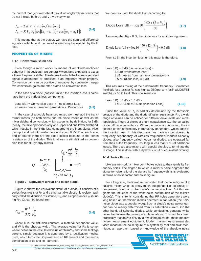
Figure 2—Equivalent circuit of a mixer diode.
Figure 2 shows the equivalent circuit of a diode. It consists of aseries (loss) resistor RS and a time-variable electronic resistor, typi-cally called the diffusion resistance, RD, and a capacitance CD shunt-ing RD. CD can be found from
(1-6)
where D is the diffusion constant, a material-dependent value,and W is the physical width. The average value for RD is some-where between the calculated value of 26 mV/ID and some leakagecurrent, simply because it is generated by a rectification mecha-nism, which turns the LO power into an RF current and then into acombination of dc and RF currents.
We can calculate the diode loss according to:
(1-7)
Assuming that RS = 8 Ω, the diode loss for a diode-ring mixer,
(1-8)
From (1-5), the insertion loss for this mixer is therefore:
Loss (dB) = 3 dB (conversion loss) +1.5 dB (transformer loss) +1 dB (losses from harmonic generation) +
0.5 dB (diode loss) = 6 dB (1-9)
This assumes mixing at the fundamental frequency. Sometimesthe diode loss resistor RS is as high as 25 Ω per arm (as in a MOSFETswitch), or 50 Ω total. This now results in
Loss (dB) = 3 dB + 1.5 dB +1 dB + 3 dB = 8.5 dB (Insertion Loss) (1-10)
Since the value of RS is partially determined by the thresholdvoltage of the diode and the diode diffusion resistance, RD, a widerange of values can be noticed for different drive levels and mixertopologies. Figure 2 shows a shunt capacitance CD, the so-calleddiode diffusion capacitance. When the diode is conducting, the in-fluence of this nonlinearity is frequency-dependent, which adds tothe insertion loss. In this discussion we have not considered itsfrequency-dependency. At wireless frequencies, modern Schottkydiodes, also frequently called hot-carrier diodes, are operated farfrom their cutoff frequency, resulting in less than 1 dB of additionallosses. There are also mixers with special circuitry to terminate theIF image. This is done with a diplexer circuit or equivalent circuitry.
1-1-2 Noise Figure
Like any network, a mixer contributes noise to the signals its fre-quency-shifts. The degree to which a mixer’s noise degrades thesignal-to-noise ratio of the signals its frequency-shifts is evaluatedin terms of noise factor and noise figure.
For a long time, the literature has stated that the noise figure of apassive mixer, which is pretty much independent of its circuit ar-rangement, is equal to the mixer’s conversion loss. But this ne-glects the influence of the white-noise contribution of the mixer’sdiode(s). This is ironic, considering that RF noise generators werelong based on thermionic diodes operated in saturation (the 5722noise diode was a popular type). Such a diode’s noise-power out-put can be readily determined from its saturation current. On theother hand, all Schottky diodes, while conducting, generate whitenoise that follows the same principle as above. This fact has beenpractically recognized only by a few companies that make modernnoise-measurement equipment. Modern noise-measurement de-vices measure the noise figure of a system by “hot and cold” tech-nique, an approach based on knowledge of the absolute noise

[ 45 ]
201 McLean Boulevard • Paterson, New Jersey 07504 • Tel: (973) 881-8800 • Fax: (973) 881-8361E-Mail: [email protected] • World Wide Web: http://www.synergymwave.com
energy emitted under hot conditions (conductance). This methodhas the advantage that it can be used up to several tens of giga-hertz, while the old vacuum-tube-based noise generators ran out ofsteam at around 1 GHz due to the inability to match the tube to the50-Ω termination. This was typically accomplished by connecting a50-Ω resistor between anode and ground (without dc connection),followed by a low-pass filter, which would match the tube capaci-tance and other parasitics to the required termination of 50 Ω, purelyresistive.
In reality, we can take the loss calculation from above and addthe Schottky noise generated by the diodes as they are driven bythe local oscillator.
If a Schottky diode is used as a noise generator in the conductivemode, it generates a continuous frequency spectrum, possibly upto several gigahertz. There is a mathematical relationship betweenthe noise power spectrum emitted by the diode and the time-aver-aged current of this diode, which generates the noise. If the noisesource impedance is set (typically 50 Ω), the available noise powercan be calculated according to:
(1-11)
wheree = 1.6 × 10⁻¹⁹ coulombsIs = saturation current of the diode∆f = effective noise bandwidthFor S11 = 0 or proper termination of this circuit (RG = Rterm):
(1-12)
Calculated at a bandwidth of 1 Hz:
(1-13)
If
(1-14)
the noise factor becomes
(1-15)
If the values for e and kT0 are inserted,
(1-16)
Example. Assume the passive mixer mentioned above with its 6-dB conversion loss is considered and a dc current of 15 mA resultsas a function of the LO drive. Since ID gets cancelled, the noisefactor (F) of the diode portion equals
(1-17)
The noise figure, NF, is 10 log F, or 0.413 dB. Now this numberand the insertion loss must be added. The resulting noise figurewould be 6.413 dB. This is consistent with published measurementdata.
Exact mathematical nonlinear approach. The exact noise factorof a real mixer is computed by the formula
(1-18)
where
N0(ωIF) = total noise power (per unit bandwidth) delivered to theIF load at intermediate frequencyKB = Boltzmann’s constantT0 = Reference temperature (290 or 300 K is commonly used)GTc(ωRF) = Transducer conversion gain from ωRF to ωRF.Let us now further elaborate on (1-18). We may write
(1-19)
where NS is noise-generated by the RF source resistance andtransferred to the IF load through frequency conversion, NINT is noisegenerated internally to the mixer, and NL is noise generated by theIF termination. If the source resistance is held at temperature T0,NS will basically originate from noise generated at the RF and im-age frequencies, which are transferred to the IF with approximatelythe same conversion loss, plus a relatively small contribution trans-ferred from other sidebands with a smaller conversion loss. Wemay then write synthetically
(1-20)
where a is a coefficient slightly larger than 1. NINT(ωRF) is gener-ated by transformer losses, by the diode Schottky noise and by thediode resistive parasitics, and in principle may take on any value; inparticular, it may be zero if both the transformers and the diodes areideal (that is, if the latter are pure nonlinear resistors). As for NL(ωIF),by Nyquist’s theorem the IF load resistor RL may be described as anoiseless resistor in series with a noise voltage source whose

[ 46 ]
201 McLean Boulevard • Paterson, New Jersey 07504 • Tel: (973) 881-8800 • Fax: (973) 881-8361E-Mail: [email protected] • World Wide Web: http://www.synergymwave.com
mean-square voltage (per unit bandwidth) is
(1-21)
where TL is the IF termination temperature. If the IF load is drivenby a source with an output impedance Zout(ωIF), the noise poweractually delivered to the load will obviously be
(1-22)
In addition to Nout, the thermal noise originating from the IF termi-nation delivered to the IF load at ωIF will also include contributionsfrom other sidebands that are back-converted by the mixernonlinearities with a relatively small conversion gain. Thus we maywrite
(1-23)
where b is slightly larger than 1. If we now introduce the mixerconversion loss, namely
(1-24)
and combine (1-18) with (1-19), (1-20) and (1-23), we finally getthe noise factor expression
(1-25)
In the normal region of operation of the mixer (sufficient LO drive)we may assume
(1-26)
so that (1-25) becomes
(1-27)
Multiplying the log10 of F by 10 gives us the exact mixer noisefigure in dB.
Table 1-1 shows how the noise figure and conversion loss varywith LO power for a generic diode DBM (Figure 3). “Starving” a di-ode mixer by decreasing its LO drive rapidly degrades its perfor-mance in all respects.
Table 1-1 Noise Figure and Conversion Lossversus LO Power for a Diode DBM
LO Power (dBm) NF (dB) Conversion Loss (dB)−10.0 45.3486 −45.1993−8.0 32.7714 −32.5264−6.0 19.8529 −19.2862−4.0 12.1154 −11.3228−2.0 8.85188 −8.055850.0 7.26969 −6.515612.0 6.42344 −5.692114.0 5.85357 −5.154046.0 5.50914 −4.844398.0 5.31796 −4.6687110.0 5.19081 −4.5496012.0 5.08660 −4.4588714.0 4.99530 −4.3880616.0 4.91716 −4.3332218.0 4.85920 −4.2940720.0 4.82031 −4.26763
Figure 3 — Generic diode DBM.
1-1-3 Linearity
1-dB compression point. Like other networks, a mixer is ampli-tude-nonlinear above a certain input level; above this point, theoutput level fails to track input-level changes proportionally. Thisfigure of merit, P−1dB, identifies the single-tone input-signal level atwhich the output of the mixer has fallen 1 dB below the expectedoutput level. The 1-dB compression point in a conventional double-balanced diode mixer is approximately 6 dB below the LO power.For Triple Balanced mixers, it is usually 3 dB below the LO power.
1-dB desensitization point. This specification is another figureof merit similar to the 1-dB compression point. However, the 1-dBdesensitization point refers to the level of an interfering (undesired)input signal that causes a 1-dB decrease in nominal conversiongain for the desired signal. For a diode-ring Doulbe Balanced Mix-ers (DBM), the 1-dB desensitization point is usually 2 to 3 dB belowthe 1-dB compression point.
Dynamic range. The dynamic range of any RF/wireless systemcan be defined as the difference between the 1-dB compressionpoint and the MDS (minimum discernible signal). These two pointsare specified in units of power (dBm), giving dynamic range in dB.When the RF input level approaches the 1-dB compression point,harmonic and intermodulation products begin to interfere with thesystem performance. High dynamic range is obviously desirable,but cost, power consumption, system complexity, and reliability mustalso be considered.

[ 47 ]
201 McLean Boulevard • Paterson, New Jersey 07504 • Tel: (973) 881-8800 • Fax: (973) 881-8361E-Mail: [email protected] • World Wide Web: http://www.synergymwave.com
Harmonic intermodulation products (HIP). These are spuriousproducts that are harmonically related to the fLO and fRF input sig-nals.
(1-28)
Table 1-2 shows relative harmonic intermodulation product lev-els for a high-level diode DBM.
Intermodulation distortion (IMD). Nonlinearities in the mixer de-vices give rise to intermodulation distortion products whenever twoor more signals are applied to the mixer’s RF port. Testing this be-havior with two (usually closely spaced) input signals of equal mag-nitude can return several figures of merit depending on how theresults are interpreted. A mixer’s third-order output intercept point(IP3,out) is defined as the output power level where the spurioussignals generated by (2fRF1 ± fRF2) ± fLO and (fRF1 ± 2fRF2) ± fLO
are equal in amplitude to the desired output signal asshown in Figure 4.
Table 1-2 Typical Spurious Responses of High-Level Double-Balanced Mixer (Decibels Below fLO±fRF Response)
RFInput SignalHarmonics fLO 2fLO 3fLO 4fLO 5fLO 6fLO 7fLO 8fLO
8fRF 100 100 100 100 100 100 100 100 1007fRF 100 97 102 95 100 100 100 90 1006fRF 100 92 97 95 100 100 95 100 1005fRF 90 84 86 72 92 70 95 70 924fRF 90 84 97 86 97 90 100 90 923fRF 75 63 66 72 72 58 86 58 802fRF 70 72 72 70 82 62 75 75 100fRF 60 0 35 15 37 37 45 40 50
60 60 70 72 72 62 70 70
Figure 4 — Mixer linearity evaluation, including compressionand two-tone IMD dynamic range. P−−−−−1dB for a single-tone can-not be read directly from this graph because the values shownare the result of two-equal-tone drive.
The third order input intercept point, IP3,in—IP3 referred to theinput level—is of particularly useful value and is the most commonlyused mixer IMD figure of merit. IP3,in can be calculated accordingto:
IPn,in = IMR ¸ (n-1) + input power (dBm) (1-29)
where IMR is the intermodulation ratio (the difference in dB be-tween the desired output and the spurious signal, and n is the IMorder—in this case, 3). In a conventional diode double-balanced
mixer, IP3,in is approximately 14 dB above the single-tone 1-dB com-pression point (P-1dB)—approximately 8 dB greater than the localoscillator power.
Although designers are usually more concerned with odd-orderIM performance, second-order IM can be important in widebandsystems (systems that operate over a 2:1 or greater bandwidth).
1-1-4 LO Drive Level
A mixer’s specifications are usually guaranteed at a particular LOdrive level, usually specified as a dBm value that may be qualifiedwith a tolerance. Insufficient LO drive degrades mixer performance;excessive LO drive degrades performance and may damage mixerdevices. Commercially available diode mixers are often classifiedby LO drive level; for example, a “Level 17” mixer requires 17 dBmof LO drive.
1-1-5 Interport Isolation
In a mixer, isolation is defined as the attenuation in dB between asignal input at any port and its level as measured at any other port.High isolation numbers are desirable. Figure 5 shows LO-to-IF andLO-to-RF isolation versus frequency for a triple-balanced diodemixer. Isolation is dependent mainly on transformer and physicalsymmetry, and device balance, but the level of signals applied tothe mixer also plays a role, as shown in Figure 6.
Figure 5 — LO-IF and LO-RF isolation versus frequency for ahigh-level triple-balanced diode mixer.
Figure 6 — LO-IF isolation versus frequency and LO drivelevel for a high-level diode DBM.
[ 48 ]
201 McLean Boulevard • Paterson, New Jersey 07504 • Tel: (973) 881-8800 • Fax: (973) 881-8361E-Mail: [email protected] • World Wide Web: http://www.synergymwave.com
1-1-6 Port VSWR
The load presented by a mixer’s ports to the outside world can beof critical importance to a designer. For example, high LO-port VSWRmay result in inefficient use of available LO power, resulting in LOstarvation (underdrive) that degrades the mixer’s performance. Fig-ure 7 shows LO-port return loss versus frequency for a high-leveldiode DBM with two values of LO power. Like interport isolation,port VSWR can vary with the level of the signal applied.
Figure 7 — LO-port return loss versus frequency for ahigh-level diode DBM.
1-1-7 Dc Offset
Isolation between ports plays a major role in reducing dc offset ina mixer. Like isolation, dc offset is a measure of the unbalance ofthe mixer. In phase-detector and phase-modulator applications, dcoffset is a critical parameter.
1-1-8 Dc Polarity
Unless otherwise specified, mixers with dc output are designedto have negative polarity when RF and LO signals are of equal phase.
1-1-9 Power Consumption
Circuit power consumption is always important, but in battery-powered wireless designs it is critical. Mixer choice may be signifi-cant in determining a system’s power consumption, sometimes inways that seem paradoxical at first glance. For instance, a passivemixer might seem to be a power-smart choice because it consumesno power—until we factor in the power consumption of the circuitryneeded to provide the (often considerable) LO power a passive mixerrequires. If a mixer requires a broadband resistive termination thatwill be provided by a post-mixer amplifier operating at a high stand-ing current, the power consumption of the amplifier stage must beconsidered as well. Evaluating the suitability of a given mixer typeto a task therefore requires a grasp of its ecology as well as itsspecifications.
The simple single-diode-mixer circuit shown in Figure 1-1 is in-tended only as an illustration of the basic behavior of diode mixer. Apractical single-diode mixer would include filtering at its RF, LO andIF ports—RF filtering for image rejection, reduced LO radiation andoptimum matching of the RF source to the diode; LO filtering tokeep RF out of the LO and optimally match the LO to the diode, andIF filtering to optimally match the diode to its IF (and IF image) load,preferably while providing some rejection of the mixer’s unwanted
outputs, the strongest (and most potentially troublesome) of whichis the LO signal.
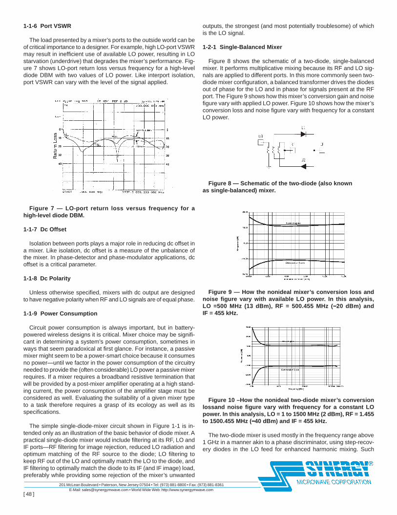
1-2-1 Single-Balanced Mixer
Figure 8 shows the schematic of a two-diode, single-balancedmixer. It performs multiplicative mixing because its RF and LO sig-nals are applied to different ports. In this more commonly seen two-diode mixer configuration, a balanced transformer drives the diodesout of phase for the LO and in phase for signals present at the RFport. The Figure 9 shows how this mixer’s conversion gain and noisefigure vary with applied LO power. Figure 10 shows how the mixer’sconversion loss and noise figure vary with frequency for a constantLO power.
Figure 8 — Schematic of the two-diode (also knownas single-balanced) mixer.
Figure 9 — How the nonideal mixer’s conversion loss andnoise figure vary with available LO power. In this analysis,LO =500 MHz (13 dBm), RF = 500.455 MHz (−−−−−20 dBm) andIF = 455 kHz.
Figure 10 –How the nonideal two-diode mixer’s conversionlossand noise figure vary with frequency for a constant LOpower. In this analysis, LO = 1 to 1500 MHz (2 dBm), RF = 1.455to 1500.455 MHz (−−−−−40 dBm) and IF = 455 kHz.
The two-diode mixer is used mostly in the frequency range above1 GHz in a manner akin to a phase discriminator, using step-recov-ery diodes in the LO feed for enhanced harmonic mixing. Such

[ 49 ]
201 McLean Boulevard • Paterson, New Jersey 07504 • Tel: (973) 881-8800 • Fax: (973) 881-8361E-Mail: [email protected] • World Wide Web: http://www.synergymwave.com
mixers are mainly used in medium-cost spectrum analyzers or mi-crowave receivers up to several tens of gigahertz, with the neces-sary transformers and baluns printed on the circuit board.
With perfectly matched diodes and perfect transformer and con-structional symmetry, no LO energy arrives at the IF and RF ports,and there is only slight attenuation between the RF and IF ports.Both building and computer modeling such a mixer is impossible:building, because perfectly matched diodes and perfect transformerand constructional symmetry cannot be achieved in practice; com-puter modeling, because floating-point mathematics runs out of gasin handling the infinite amplitude spread involved in calculating theperfect cancellation of the LO signal as it travels to the RF and IFports. That said, Figure 11 compares the mixer’s quasi-ideal port-to-port isolation (matched diodes, a perfect transformer, no strayinductances and capacitances, and a 10-megohm resistors con-nected from port to port) and nonideal port-to-port isolation (slightlymismatched diodes and 0.5 pF between the upper terminal of themiddle winding and ground).
Figure 11 — Port-to-port isolation of the quasi-ideal (identi-cal diodes and no stray capacitance) and nonideal (slightlymismatched diodes and 0.5 pF of stray capacitance betweenthe upper terminal of the middle transformer windingand ground) two-diode mixer. In this analysis, LO = 1 to 1500MHz (2 dBm), RF = 1.455 to 1500.455 MHz (−−−−−40 dBm) andIF = 455 kHz.
Figure 12 — The nonideal mixer’s output spectrum with (a)identical diodes and no stray capacitance and (b) slightly mis-matched diodes and 0.5 pF of stray capacitance between the
upper terminal of the middle transformer winding and ground.In these analyses, LO = 310.7 MHz (2 dBm), RF = 300.0 MHz (−−−−−40 dBm) and IF = 10.7 MHz. Four LO harmonics and 3 LO side-bands were used.
Figures 12a and 12b show the mixer’s output spectrum for thequasi-ideal and nonideal cases, respectively.
1-2-1 Subharmonically pumped single-balanced mixer.
Figure 13 shows a single-balanced mixer with a difference: anti-parallel diode pairs take the place of single diodes, the RF and IFare buffered from each other only by filtering, and the LO is appliedat 1/2 the frequency necessary to provide the desired frequencyconversion. The RF-to-IF isolation is limited to that provided by theseriesed input and output filtering, but the LO-to-IF isolation is higherat fLO, and much higher at 2fLO, than that achievable with a DBMwith the LO signal at 2fLO (Figure 14). Although the example shownis for an up-converting HF receiver, this technique finds applicationwell into the microwave range as the basis for I/Q modulators, inwhich carrier leakage must be reduced to a level difficult to achievewith conventional DBMs.
Figure 13 — A subharmonically pumped single-balancedmixer using antiparallel diode pairs. The LO operatesfrom 40.005 - 55.005 MHz to mix 0.01 - 30.01-MHz RF to anIF of 80 MHz.
Figure 14 —Simulated interport isolation of the subharmonicSBM. For realism, the diodes and transformers are slightlymismatched.

[ 50 ]
201 McLean Boulevard • Paterson, New Jersey 07504 • Tel: (973) 881-8800 • Fax: (973) 881-8361E-Mail: [email protected] • World Wide Web: http://www.synergymwave.com
2-1-1 Diode-Ring Double Balanced Mixer
Adding two more diodes and another transformer to the singlybalanced mixer results in a double-balanced mixer (DBM) as shownin Figure 15. A DBM’s frequency response is largely determined bythe frequency response of its transformers. The low-frequency limitis determined by the inductance of the transformer windings, thereactance of which, at the lowest frequency of interest, should be atleast four times the impedance at which the transformer operates.The upper frequency limit is determined mainly by the degradationof the transformers’ transmission-line behavior at higher frequen-cies, although the increasing importance of diode capacitance alsoplays a role.
Figure 15 —Schematic of the diode-ring doublybalanced mixer.
A DBM’s interport isolation is determined by the symmetry of itstransformers, diodes and physical construction. In practice, the ef-fects of diode mismatch can by minimized by using a diode quadring crossover with closely matched diode.
Figure 16 shows how the DBM’s conversion loss and noise figurevary with applied LO power. Figure 17 shows how the DBM’s con-version loss and noise figure vary with frequency for an LO powerof 7 dBm, with quasi-ideal and nonideal balance. Figure 18 showshow the DBM’s port-to-port isolation differs with quasi-ideal andnonideal balance for an LO power of 7 dBm. Figure 19 shows howthe DBM’s RF- and LO-port return loss varies with frequency; thesharp peak corresponds to a resonance caused by one of the straycapacitances added to simulate less-than-ideal balance in the mod-eled mixer.
Figure 16 — DBM conversion gain and noise figure versusLO power. In this analysis, LO = 310.7 MHz (−−−−−10 to 26 dBm), RF= 300 MHz (−−−−−40 dBm) and IF = 10.7 MHz.
Figure 17 — This plot of conversion gain and noise figureversus frequency for quasi-ideally and nonideallybalancedversions of the same DBM reveals that balance playsarelatively minor role in the CG and NF performance achieved.Inthese analyses, the LO (−−−−−7 dBm) sweeps from 1 MHz to 1500MHz and the RF (−−−−−40 dBm) sweeps from 1.455 to 1500.455 MHzto produce an IF of 455
Figure 18 — Interport isolation for DBMs with quasi-ideal andnonideal balance. In these analyses, the LO (−−−−−7 dBm)sweepsfrom 1 MHz to 1500 MHz and the RF (−−−−−40 dBm) sweepsfrom 1.455 to 1500.455 MHz to produce an IF of 455 kHz.
Figure 19 — Return loss versus frequency for the DBM’s RFand LO ports. The sharp peak results from a stray resonance.

[ 51 ]
201 McLean Boulevard • Paterson, New Jersey 07504 • Tel: (973) 881-8800 • Fax: (973) 881-8361E-Mail: [email protected] • World Wide Web: http://www.synergymwave.com
Figure 20 — Output spectrum of a nonideally balanced DBM.In this analysis, LO = 310.7 MHz (−−−−−7 dBm) and RF = 300 MHz(−−−−−40 dBm) for an IF of 10.7 MHz. Four LO harmonics and 3 LOsidebands were used.
Figure 21 — IF-port voltage waveform of the DBM over 100cycles of the LO signal. The 310.7-MHz LO and 10.7-MHz IFcomponents are clearly evident.
Figure 20 shows the DBM’s output spectrum. Figure 21 showsthe DBM’s output waveform over 50 cycles of the LO signal.
Two-tone testing the DBM allows us to characterize its IP3 figuresof merit. Figure 22 shows the nonideal DBM’s IF and IM3 responsesfor LO powers of −5, 1, 7 and 13 dBm. Figure 23 details how theDBM’s IP3 increases with LO drive, and Figure 24 shows the de-sired IF outputs and close third-order spurs near 10.7 MHz. Figure25 shows the DBM’s output voltage over 100 cycles of the LO sig-nal, and Figure 26 shows the anode-cathode voltage of one of thering’s diodes, also over 100 LO cycles, both under two-tone IMDtest conditions.
Figure 22 — Diode DBM IF and IM3 output versus RF powerfor four LO-drive levels. The responses for LO = 7 dBm havebeen extrapolated to show IP3. Within limits, varying a mixer’s
LO drive affects its linear IF output relatively little while signifi-cantly affecting IMD. See Figure 23. For all four analyses,LO = 310.7 MHz, RF1 = 300.0 MHz (−−−−−40 to 10 dBm), and RF2 =300.3 MHz (−−−−−40 to 10 dBm); 4 LO harmonics and 3 LO side-bands were used.
Figure 23 — Extrapolating the responses for all four LO lev-els represented in Figure 22 shows how varying a diode DBM’sLO drive shifts its third order intercept point. Although thesecurves indicate that the simulated mixer’s IP3 generally in-creases with LO drive, the improvement in IP3 is not as greatas we might expect. The reason for this is that these four analy-ses, as well as the other diode-mixer analyses in this chapter,were done using diode models with a threshold voltage (VJ) of0.23. If high-level diodes with a VJ of about 0.8 V had been used,IP3,out for the 13 dBm LO case shown here would increase to+13 dBm. IP3,in for the 13 dBm LO case would turn out to be 13dBm + insertion loss = 13 dBm + 7 dB = 20 dBm. The issue ofdiode damage aside, attempting to increase IP3 merely by driv-ing a low- or medium-barrier diode harder eventually results indiminishing returns. High-barrier diodes are essential in get-ting the best IP3 performance with high LO drive.
Figure 24 — The DBM’s output in the 11-MHz region duringtwo-tone testing. The third-order products are clearly visibleabove and below the desired output signals. The test condi-tions for this analysis are those for Figure 22 with LO = 13 dBm.

[ 52 ]
201 McLean Boulevard • Paterson, New Jersey 07504 • Tel: (973) 881-8800 • Fax: (973) 881-8361E-Mail: [email protected] • World Wide Web: http://www.synergymwave.com
Figure 28 — A mixer with a dc-coupled IF port can be usedas a phase detector.
Figure 29 — A diode-ring mixer as phase modulator.
Figure 30 — Two biphase modulators form the basis for aQPSK modulator.
Figure 25 — The DBM’s IF-output voltage over 50 cycles ofthe LO signal. The test conditions for this analysis are thosefor Figure 28 with LO = 13 dBm.
Figure 26 — The anode-cathode voltage of one of the DBM’sdiodes, also over 50 LO cycles under two-tone IMD testcondtions. The test conditions for this analysis are those forFigure 4-28 with LO = 13 dBm.
A double-balanced mixer, unless it is termination insensitive, isextremely sensitive to nonresistive termination. This is because thetransmission-line transformers do not operate properly when theyare not properly terminated, and the reflected power generates highvoltage across the diodes. This effect results in much higher distor-tion levels than in a properly terminated transformer.
2-2 Applications of mixers
2-2-1 Phase detector. Theoretically, any mixer with a dc-coupledIF port can be used as a phase detector. When two signals of equalfrequency are applied simultaneously to the reference and incom-ing signal ports, the phase detector produces a dc output at the IFport proportional to the cosine of the phase difference (Figure 28).
2-2-2 Binary phase-shift keying (BPSK) modulator. Binaryphase modulation occurs when a positive and negative signal cur-rent shifts the RF carrier between 0 and 180°. Figure 29 shows adouble-balanced mixer operating as a BPSK modulator.

[ 53 ]
201 McLean Boulevard • Paterson, New Jersey 07504 • Tel: (973) 881-8800 • Fax: (973) 881-8361E-Mail: [email protected] • World Wide Web: http://www.synergymwave.com
Figure 31 — Quadrature mixer.
Figure 32 — An image-reject mixer uses phasing to differen-tiate between its LO+IF and LO−−−−−RF IF outputs.
Figure 33 — A diode DBM can be used as a dc-controlledattenuator if PIN diodes are used instead of Schottky devicesin its ring.
2-2-3 Quadrature phase-shift keying (QPSK) modulator. A typi-cal QPSK Modulator consists of two biphase modulators, a 90° di-vider, and a 0° power combiner as shown. Data inputs at the controlports will cause the carrier to shift between 0, 90, 180 and 270° asshown in Figure 30.
2-2-4 Quadrature IF mixer. A quadrature IF Mixer produces twoIF outputs in phase quadrature. Its basic structure consists of twodouble balanced mixers, a 90° splitter and 0° splitter. The basicblock diagram is shown in Figure 31.
2-2-5 Image-reject mixer. The image-reject mixer consists of abasic quadrature IF mixer with an additional 90° hybrid at the IFports as shown in Figure 32. The primary function is to differentiatebetween the real signal and the image signal. This type of device isespecially useful in applications where the desired RF signal andimage are so close in frequency that rejecting the image withfiltering is not practical.
2-2-6 Diode attenuator/switch. A ring of PIN diodes can be usedas electronic attenuators by applying variable forward bias to thediodes (Figure 33). Maximum attenuation is achieved when the cur-rent at the control port is zero. The maximum attenuation is theisolation between the input and output port. Minimum attenuation(insertion loss) is achieved when the IF port current is 20 mA.
2-2-7 Single-sideband (SSB) or in-phase/quadrature (I/Q)modulator. SSB or I/Q modulators are useful in discriminating andremoving the lower sideband (LSB) or upper sideband (USB) gen-erated during frequency conversion, especially when the sidebandsare very close in frequency and attenuation of one of the sidebandscannot be achieved with filtering. This is the case with audio andvideo modulation, where signals from dc to 10 MHz must be con-verted to a higher frequency that is appropriate for transmission. Insuch cases, both sidebands will be very close in frequency to thecarrier frequency. With an I/Q modulator, one of the sidebands iseasily cancelled or attenuated along with its carrier.
Attenuation of the carrier has been the most troublesome aspectin the design of passive I/Q modulators. Isolation between the lo-cal-oscillator (LO) port and the RF port of the mixers, which is themain parameter in determining carrier rejection, is usually insuffi-cient at frequencies above 200 MHz.
Figure 34 — An SSB modulator matches two high-frequencymixers, a 90°°°°° hybrid, and an in-phase power combiner to pro-duce an SSB output signal.
I/Q modulator designs have basically comprised two double-bal-anced mixers (Figure 34). The mixers are fed at the LO ports by acarrier phase-shifted through a 90°. hybrid. Thus, the carrier signal’srelative phase is 0° to one mixer and 90° to the other mixer. Modu-lation signals are fed externally in phase quadrature to the two mix-ers’ IF ports. The mixers’ modulated output signals are combinedthrough a two-way, in-phase power divider/combiner.
The circuit forms a phase-cancellation network to one of the side-bands and a phase-addition network to the other sideband. Thecarrier is somewhat attenuated and is directly dependent on theinherent LO-to-RF isolation of the mixers and the modulating signallevel. In industry-standard I/Q modulators, USB suppression resultswhen the first modulation port (MOD 1) is fed with a signal that is90° in advance of the signal feeding the second modulation port(MOD 2). Opposite phasing can be arranged by changing the inter-nal phase polarity of the mixers or by interchanging the 90° hybridoutput ports to the LO ports of the mixers.

[ 54 ]
201 McLean Boulevard • Paterson, New Jersey 07504 • Tel: (973) 881-8800 • Fax: (973) 881-8361E-Mail: [email protected] • World Wide Web: http://www.synergymwave.com
The phase and amplitude imbalancesbetween the various components used inthe manufacturing of the I/Q modulatorsmust be tightly maintained for optimumSSB rejection. Matching of the two mix-ers for conversion loss and insertionphase is extremely critical, since differ-ences in these parameters will add toamplitude- and phase-imbalance errors.The 90° hybrid in the LO port must be innearly perfect phase quadrature.
Phase- and amplitude-imbalance errorsadversely affect sideband suppression(Figure 35). In most cases, a typical pas-sive I/Q modulator operates with a carrierinput level of +10 dBm, which is requiredto drive the diodes in the mixers to oper-ate in the linear range. The dynamic rangeof these mixers can be significantly im-proved by using diodes with a higher bar-rier height. The LO signal in this case mustbe increased in order to drive these di-odes into conduction in their linear range.Carrier rejection is also a problem whendesigning an SSB modulator, since onlya few decibels of suppression can beachieved in standard high-frequency mod-els. The major contributor to carrier sup-pression is the inherent LO-to-RF isola-tion through the mixers. Unfortunately, this isolation is usually poorat cellular frequencies (800 to 1000 MHz), where at least 25 dB ofcarrier rejection is necessary. In some cases, designers feed asmall amount of dc into the IF ports to control the carrier rejection,but this complicates the driver circuitry and calls for temperaturecompensation when operating at different temperatures. As anexample, an SSB modulator is assumed to operate with +10-dBmLO drive with each modulating signal at −10 dBm and in phasequadrature to each other when applied to the modulating ports(MOD 1 and MOD 2). The result will be a modulated signal at −16dBm, assuming 6-dB conversion loss. For 20-dB carrier rejectionwith respect to the desired modulated signal, the carrier must beat −36 dBm, which translates to LO-to-RF isolation of 46 dB.
For 20-dB carrier rejection with respect to the desired modu-lated signal, the carrier leakage must be at −36 dBm, which trans-lates to LO-to-RF isolation of 46 dB.
By employing a subharmonic approach, the performance of SSBmodulators can be extended beyond the limits of conventional de-signs. The approach is based on the use of subharmonic mixers inplace of Double Balanced-frequency mixers and is applicable fromabout 140 to 3000 MHz. Matched antiparallel diode pairs used insingle-ended or single-balanced mixer configurations cancel even-order intermodulation products (such as 2fLO × 2fRF, 3fLO × 3fRF,etc.) at all ports.
Single-ended mixers lack the port-to-port isolation needed forSSB modulator applications. Odd-order products of the RF andLO frequencies (even fLO × odd fRF) and (odd fLO × even fRF) ap-pear on all ports, requiring extensive filtering for satisfactory per-formance. For a single-balanced mixer, even harmonics of the LOcombining with odd harmonics of the RF appear at the IF port,whereas odd harmonics of the LO combining with even harmonicsof the RF appear at the RF and IF ports. This assumes that a
balanced transformer is placed at the LO port, which is a logicalchoice due to the fact that the highest level signal appears at theLO port. Since the desired odd-order IF products appear at both theRF and IF ports, a need arises for a diplexing network to isolate theRF and IF signals.
The subharmonic modulator design provides a unique way to iso-late the RF and IF signals. A single-balanced harmonic mixer offersgood LO-to-RF and LO-to-IF isolation but poor RF-to-IF isolation.Fortunately, harmonically related signals are spaced well apart inthe frequency spectrum, simplifying filtering of harmonically relatedsignals.
Harmonic mixing also works well with low LO power levels, withsomewhat lower 1-dB compression on the RF port than with funda-mental-frequency mixing. The ability to operate with LO frequen-cies that are a fraction of the carrier frequency (1/2, 1/4, 1/6, etc.)significantly reduces the cost of an LO source, especially at higherfrequencies. Also, using lower-frequency LO sources helps avoidthe signal-leakage problems inherent with higher-frequency LOsources. Minimizing signal leakage, especially at higher frequen-cies, becomes expensive and bulky. Subharmonic mixing offersseveral advantages:
• The technique offers the ability to operate at LO frequen-cies that are 1/2, 1/4, or 1/6 of the carrier frequency. For ex-ample, for an IF of 100 MHz at an RF of 2 GHz, the LO can be(2000±100) ÷ 2 = 950 or 1050 MHz.
• The LO’s even harmonics are strongly attenuated.• The filtering requirements for fundamental frequency and
odd harmonic signals of the LO are not critical.• The cost of generating the LO is reduced due to the fact
that the LO frequency need only be a fraction of the carrierfrequency.
As an example of the performance improvements possible withthe subharmonic mixers, units were evaluated at both cellular (935-to 960-MHz) and PCN/PCS (1.8- to 1.9-GHz) bands. For a conven-tional SSB modulator at 1.9 GHz fed with +10 dBm modulation sig-nals, carrier rejection is barely 10 dB (36).
Figure 36 — This plot of carrier and sideband rejection wasmeasured for a conventional SSB modulator operatingat 1.9 GHz.
Figure 35 — Thelevel of SSBrejection improvesas the phase andamplitude imbal-ance performanceof an SSB modula-tor improves.

[ 55 ]
201 McLean Boulevard • Paterson, New Jersey 07504 • Tel: (973) 881-8800 • Fax: (973) 881-8361E-Mail: [email protected] • World Wide Web: http://www.synergymwave.com
Figures 37 — The SSB modulator’s return loss as measuredat the local-oscillator (LO) port
Figure 38 — The novel harmonic SSB modulator’s return lossas measured at the RF port.
Sideband rejection can be improved by tuning, but the carrierrejection is controlled by the LO-to-RF isolation of the double-bal-anced mixers. Conventional double-balanced mixers with high iso-lation at cellular and PCN bands are very expensive and large whenspecial techniques are used to improve LO to-RF isolation. In con-trast, the subharmonic nature of the new approach allows the useof lower-frequency, less-expensive components in the modulators’construction.
The subharmonic modulators offer an improvement of more than15 dB in carrier suppression compared to the conventional approach.
The measured return loss at the LO and RF ports is better than18 dB (Figures 37 and 38). Measurements made on a cellular-bandSSB modulator reveal carrier rejection on the order of 40 dB.Typical insertion loss is 7 dB while sideband rejection is 30 dB(Figure 39).
Figure 39 — This plot of carrier and sideband rejection asmeasured for the novel harmonic SSB modulator operating atcellular frequencies.
By the virtue of harmonic mixing, even-order mixing products areattenuated by about 30 dB with respect to the desired modulatedoutput signal. The fundamental-frequency feedthrough into the out-
put port is approximately 5 dB lower than the desired modulatedsignal, whereas the fourth harmonic mixing with the modulating sig-nal is approximately 10 dB lower. Typical loss for fourth-harmonicmixing is 17 to 19 dB while maintaining 30 dB of carrier rejection.
Since harmonically-related products are well-spaced in frequency,filtering undesired signals is relatively inexpensive using standardoctave-bandwidth filters. Low-cost commercial bandpass filters typi-cally offer better than 40 to 50 dB attenuation of unwanted har-monic signals. Constant-impedance bandpass filters offering goodimpedance match at desired stopbands can also be used in caseswhere harmonically related products require impedance termina-tion within a system.
The subharmonic modulator design is easily applied at customfrequencies. Conversion of an SSB modulator with output frequencycorresponding to twice the LO frequency to one with output corre-sponding to four times the LO frequency requires only one compo-nent change, in the form of a signal-combining network at themodulator’s output. Although the conversion loss of the fourth-har-monic LO component mixing with the modulating signal is in thevicinity of 18 dB, the cost of generating the LO is drastically re-duced with the subharmonic modulator. In spite of higher signalloss, the carrier rejection is still at least 30 dB at the fourth har-monic, and harmonically related products can be eliminated withan inexpensive filter.
2-2-8 Triple-balanced mixer. Two diode rings can be combinedto form a double double-balanced mixer, or triple-balanced mixer(TBM), as shown in Figure 40. Triple-balanced mixers achievegreater higher dynamic range and interport isolation than double-balanced designs especially above 1 GHz at the expense of LOpower and increased complexity and size. The conversion loss ofTriple Balanced mixers increases by approximately 6 dB as the IFfrequency is lowered below the sampling LO/RF frequency towardsDC.
Figure 41 shows the circuit’s interport isolation with the circuitconfigured in a less than ideally balanced form, with small varia-tions in transformer-winding inductance and diode parameters in-troduced for more realistic modeling. Note that the mixer’s interportisolation generally less sloped with frequency, when compared withthe DBM (Figure 42).
Figure 40—A triple-balanced diode mixer. A limitation of thisconfiguration is that the internal dc common connections as-sociated with its RF and LO transformers disallow usable IFresponse down to dc.

[ 56 ]
201 McLean Boulevard • Paterson, New Jersey 07504 • Tel: (973) 881-8800 • Fax: (973) 881-8361E-Mail: [email protected] • World Wide Web: http://www.synergymwave.com
Figure 41—The triple-balanced mixer offers improved high-frequency isolation over a standard DBM.
Figure 42—The Double-balanced mixer isolation for a DBM.