Embed Size (px)
Citation preview

1
Chapter 7 Mixers
• Three-terminal non-linear or time-varying devices for
frequency conversion.
• Implemented by diode and transistor in microwave
range.
• Loss, noise and inter-modulation distortion are major
parameters.
• Diode mixer and FET mixers will be introduced

2 May 16, 2008
7.1 Mixers characteristics
Frequency conversion

3
• Up-conversion
fLO + fIF being the upper sideband (USB), and fLO – fIF being the lower sideband (LSB)
A double-sideband (DSB) signal contains both upper and lower sidebands, as in (7.3), while a
single-sideband (SSB) signal can be produced by filtering or by using a single-sideband mixer.

4
• Down-conversion
Easily selected by low-pass filtering

5
• Image frequency
• Image frequency
The RF frequency defined in (7.8b) is called the image response. The image response is
important in receiver design because a received RF signal at the image frequency of (7.8b)
is indistinguishable at the IF stage from the desired RF signal of frequency (7.8a), unless
steps are taken in the RF stages of the receiver to preselect signals only within the desired
RF frequency band.
In practice, most receivers use a local oscillator set at the upper sideband, fLO = f RF + fIF,
because this requires a smaller LO tuning ratio when the receiver must select RF signals
over a given band.
6

7
Conversion loss
• 4~7dB for diode mixer at 1~10GHz
• Transistor may even have conversion gain of a few dB.
• Minimum loss for LO power at 0~10dBm.
There are inherent losses in the frequency conversion process because of the generation
of undesired harmonics and other frequency products.
8
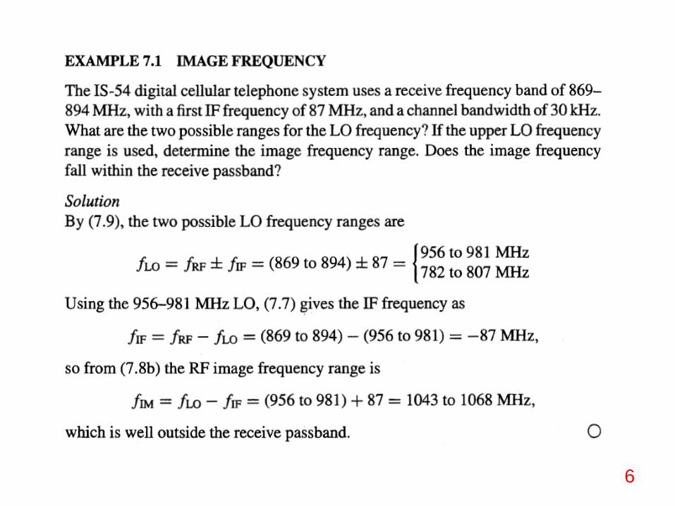
Noise figure
NF: 1~5dB typical value.
The noise figure of a mixer depends on whether its input is a single sideband signal
or a double sideband signal. This is because the mixer will down-convert noise at
both sideband frequencies (since these have the same IF), but the power of a SSB
signal is one-half that of a DSB signal (for the same amplitude).
For double side band (DSB) signal
Noise is generated in mixers by the diode or transistor elements, and by thermal sources
due to resistive losses.

9
• For single side band (SSB) signal

10
Inter-modulation distortion
Since mixers involve nonlinearity, they will produce intermodulation products.
Typical values of P3 for mixers range from 15 dBm to 30 dBm.
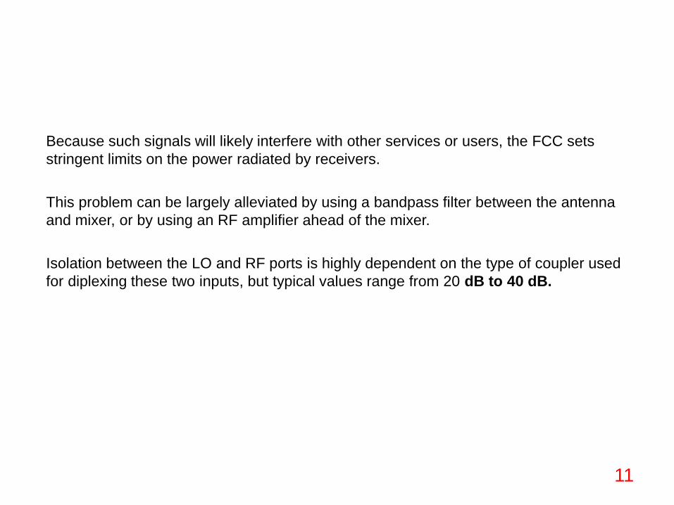
Isolation
Ideally, the LO and RF ports would be decoupled, but internal impedance mismatches and
limitations of coupler performance often result in some LO power being coupled out of the RF port.
This is a potential problem for receivers that drive the RF port directly from the antenna, because
LO power coupled through the mixer to the RF port will be radiated by the antenna.
11
Because such signals will likely interfere with other services or users, the FCC sets
stringent limits on the power radiated by receivers.
This problem can be largely alleviated by using a bandpass filter between the antenna
and mixer, or by using an RF amplifier ahead of the mixer.
Isolation between the LO and RF ports is highly dependent on the type of coupler used
for diplexing these two inputs, but typical values range from 20 dB to 40 dB.

12
7.2 Diode mixers
Small-signal diode characteristics
• Small signal, large signal and ideal switching circuit
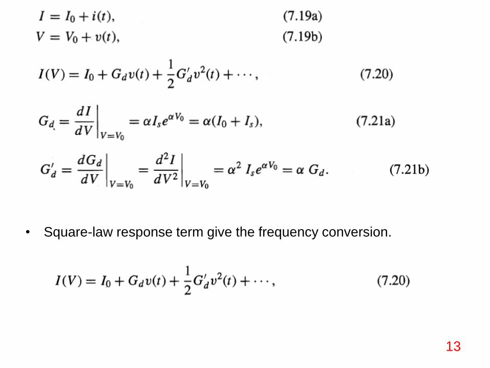
13
• Square-law response term give the frequency conversion.

14
Single-ended mixer
The RF and LO inputs are combined in a diplexer, which superimposes the two input
voltages to drive the diode. The diplexing function is easily implemented using an RF
coupler or hybrid junction to provide combining as well as isolation between the two
inputs.
The diode may be biased with a DC bias voltage, which must be decoupled from the
RF signal paths. This is done by using DC blocking capacitors on either side of the
diode, and an RF choke between the diode and the bias voltage source.
The AC output of the diode is passed through a low-pass filter to provide the desired IF
output voltage.

15

16
Large-signal
Small-signal analysis of a mixer can not accurate enough to provide a realistic result for
conversion loss.
This is primarily because the power supplied to the mixer LO port is usually large enough to
violate the small-signal approximation.
Here, a fully nonlinear analysis of a resistive diode mixer. Reactance associated with the
diode junction and package are ignored, to simplify the analysis.
Low level RF input voltage, and a much larger LO pump signal.
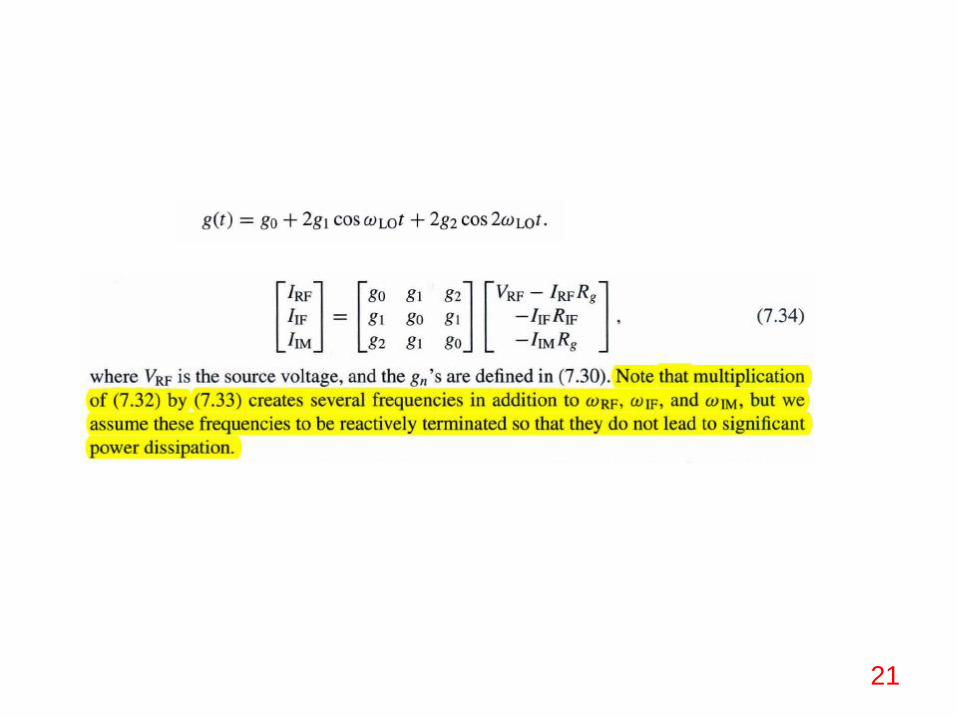
These two AC input signals generate a multitude of harmonics and other frequency products:
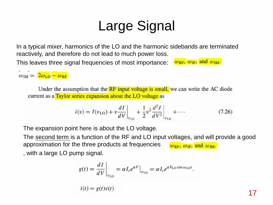
Large Signal
17
In a typical mixer, harmonics of the LO and the harmonic sidebands are terminated
reactively, and therefore do not lead to much power loss.
This leaves three signal frequencies of most importance:
The expansion point here is about the LO voltage.
The second term is a function of the RF and LO input voltages, and will provide a good
approximation for the three products at frequencies
, with a large LO pump signal.

18

Large Signal
19

20
21

22
The easiest way to find the available power from the IF port is to first find the Norton
equivalent source for the IF port.

23
The available input power from the RF source is
The available output power at the IF port is

24
The minimum conversion loss of (7.42) reduces to LC = 2, or 3 dB. This means that halt
the RF input power is converted to IF power, and half is converted to power at the image
frequency.

© M. S. Ramaiah School of Advanced Studies, Bangalore
PEMP VSD538
© M. S. Ramaiah School of Advanced Studies, Bangalore1
Mixer Circuits
Session Speaker:
D. Varun
Session 5

© M. S. Ramaiah School of Advanced Studies, Bangalore
PEMP VSD538
© M. S. Ramaiah School of Advanced Studies, Bangalore
Session Objectives
• To expound on MW and RF Mixer architectures
• To design and develop a Single Balanced / DoubleBalanced Diode Mixer & Gilbert Cell Mixer
• To illustrate various mixer performance parameters forthe developed design
• To expound on various Oscillator architectures for MWand RF frequencies
• To design and develop Hartley, Colpitts and DifferentialOscillators
• To illustrate Oscillator phase noise parameters andLeesons Equation
2

© M. S. Ramaiah School of Advanced Studies, Bangalore
PEMP VSD538
© M. S. Ramaiah School of Advanced Studies, Bangalore
Session Topics
• Introduction to RF/MW mixers
• Types of Mixers
• Unbalanced Mixer
• Balanced Mixer
• Image Reject Architectures
3
© M. S. Ramaiah School of Advanced Studies, Bangalore
PEMP VSD538
© M. S. Ramaiah School of Advanced Studies, Bangalore
RF Mixers Primer
• All RF transceiver systems require a fixed range ofelectromagnetic frequencies at any given time
• Baseband frequency at a transmitter or receiver isencoding of data to be transmitted/received into a signalat a frequency close to zero
• The process wherein signals are multiplied together andnew frequencies (IF) are generated is called RF or radiofrequency mixing
• Up-conversion is the process of translating lowerfrequency (IF) to a higher frequency (RF) and down-conversion is the process of translating RF signal to alower frequency (IF) thus enabling data extraction
4

© M. S. Ramaiah School of Advanced Studies, Bangalore
PEMP VSD538
© M. S. Ramaiah School of Advanced Studies, Bangalore
Introduction to Mixer• Mixers perform frequency translation by multiplying two signals
• Mixers are non-linear devices used in systems to translate (multiply) onefrequency to another.
• All mixer types work on the principle that a large Local Oscillator (LO) RFdrive will cause switching/modulating the incoming Radio Frequency (RF) tothe Intermediate Frequency (IF).
• The multiplication process begins by inputting two signals:
• The resulting multiplied signal will be:
5
© M. S. Ramaiah School of Advanced Studies, Bangalore
PEMP VSD538
© M. S. Ramaiah School of Advanced Studies, Bangalore
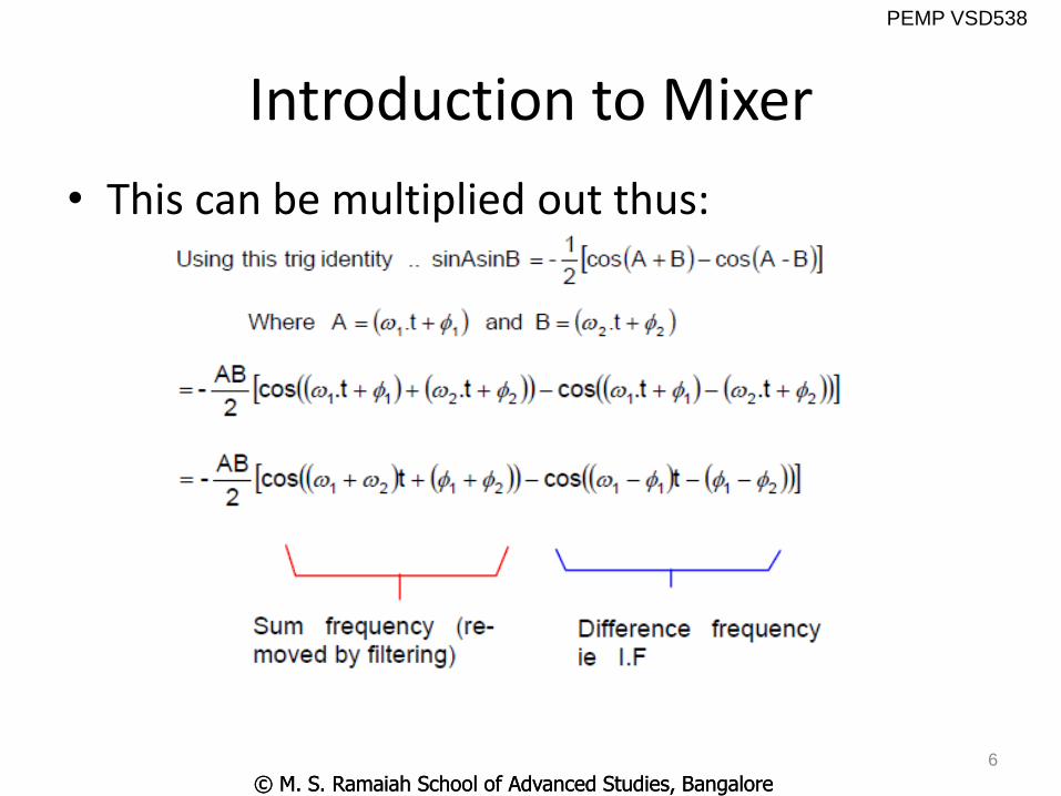
Introduction to Mixer
• This can be multiplied out thus:
6
© M. S. Ramaiah School of Advanced Studies, Bangalore
PEMP VSD538
© M. S. Ramaiah School of Advanced Studies, Bangalore
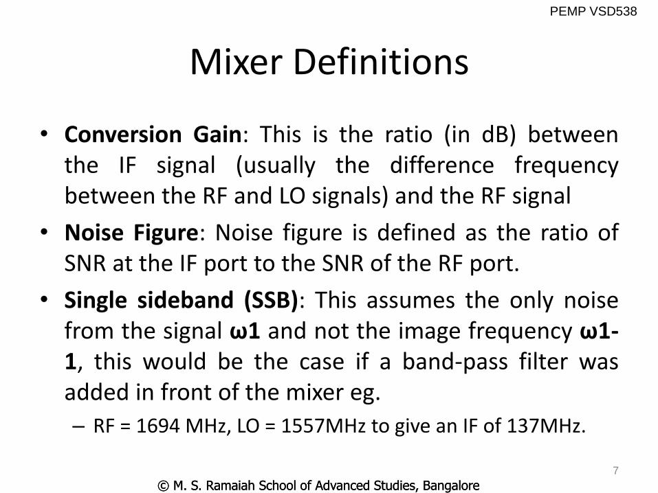
Mixer Definitions
• Conversion Gain: This is the ratio (in dB) betweenthe IF signal (usually the difference frequencybetween the RF and LO signals) and the RF signal
• Noise Figure: Noise figure is defined as the ratio ofSNR at the IF port to the SNR of the RF port.
• Single sideband (SSB): This assumes the only noisefrom the signal ω1 and not the image frequency ω1-1, this would be the case if a band-pass filter wasadded in front of the mixer eg.
– RF = 1694 MHz, LO = 1557MHz to give an IF of 137MHz.
7
© M. S. Ramaiah School of Advanced Studies, Bangalore
PEMP VSD538
© M. S. Ramaiah School of Advanced Studies, Bangalore
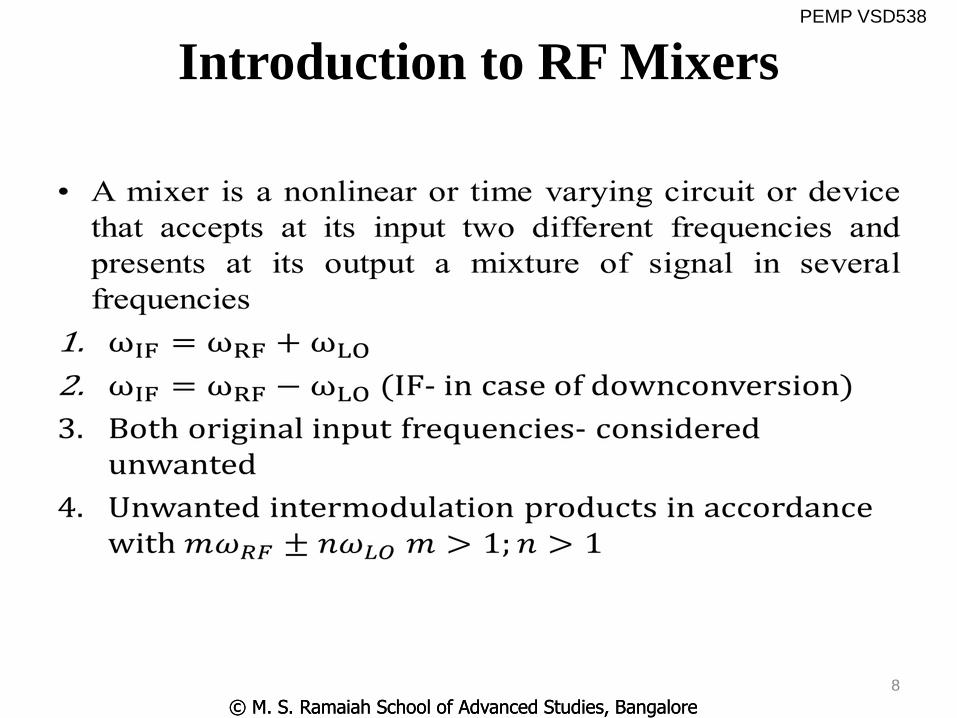
Introduction to RF Mixers
8

© M. S. Ramaiah School of Advanced Studies, Bangalore
PEMP VSD538
© M. S. Ramaiah School of Advanced Studies, Bangalore
Mixer Output Example
• When two or more signals of differing frequencies are inputto a nonlinear system, the basic nature of nonlinear systemproduces a multiplicity of output frequencies that appear atfrequencies nominally equal to the sum and difference infrequencies of the original signals
9

© M. S. Ramaiah School of Advanced Studies, Bangalore
PEMP VSD538
© M. S. Ramaiah School of Advanced Studies, Bangalore
Types of Mixers
• Mixers can be classified into two broad categories
depending on the type of nonlinear component used
viz., diode, MOS,HEMT etc..
• Active and Passive mixers are the classification based
on nonlinear components
• Mixer classification of mixers can also be based on
type of input applied
• Unbalanced and Balanced are the classes based on
input methods
10

© M. S. Ramaiah School of Advanced Studies, Bangalore
PEMP VSD538
© M. S. Ramaiah School of Advanced Studies, Bangalore
Passive & Active Mixers
• ON/OFF switch is the most common form of a RF mixer
• When ON, the RF mixer allows the signal to pass through,and when OFF it does not
• Such a mixer can be realized using any passive device likediode provided the local oscillator input is high enough toswitch the device ON
• In a passive mixer no signal propagates through when thedevice is in OFF state
• In a passive mixer the conversion loss will be 3 db
• In reality conversion losses of 6 dB to 9 dB are commonlyencountered
• Active mixers have a significant advantage over passivemixers
11

© M. S. Ramaiah School of Advanced Studies, Bangalore
PEMP VSD538
© M. S. Ramaiah School of Advanced Studies, Bangalore
Passive & Active Mixers
• Passive resistive diode mixers operate over a wide band andoffer conversion loss to the system
• Varactors operate over a narrow band and offers lowconversion gain
• These factors make the passive mixers unreliable foroperation under certain conditions
• Active multiplier mixers are used to abate the losses ofpassive mixers
• An active mixer operates over broad band widths andprovides conversion gain
• The other major advantages of high-frequency FET or BJTmixers are: multipliers devour little dc power; output ismore devoid of spurs and dissipates little heat
12
© M. S. Ramaiah School of Advanced Studies, Bangalore
PEMP VSD538
© M. S. Ramaiah School of Advanced Studies, Bangalore
Unbalanced Mixer
• A mixer functioning in any frequency requires
isolation between the ports to avoid any
intermodulation distortion
• The mixer becomes unbalanced when designed
without any port isolation
• Unbalanced mixer can be designed using a single
diode
• The local oscillator and RF signal input appear along
with the intermodulation products at the mixer output
13

© M. S. Ramaiah School of Advanced Studies, Bangalore
PEMP VSD538
© M. S. Ramaiah School of Advanced Studies, Bangalore
Unbalanced Architecture
14

© M. S. Ramaiah School of Advanced Studies, Bangalore
PEMP VSD538
© M. S. Ramaiah School of Advanced Studies, Bangalore
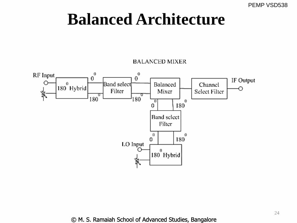
Balanced Mixer
• Grossly divided into two classes:
Singly-Balanced Mixers (SBM)
Doubly-Balanced Mixers (DBM)
• Singly-Balanced mixers use two devices, and are
usually realized as two single device mixers
connected via a 180-degree or 90-degree hybrid
• Double balanced mixers usually consist of four
untuned devices interconnected by multiple hybrids,
transformers or baluns
15

© M. S. Ramaiah School of Advanced Studies, Bangalore
PEMP VSD538
© M. S. Ramaiah School of Advanced Studies, Bangalore
Merits and Demerits
• The advantages of balanced mixers over single-device
mixers are:
Rejection of spurious responses and intermodulation
products
Better LO-to-RF, RF-to-IF and LO-to-IF isolation
Rejection of AM noise in the LO
• The disadvantage of balanced mixers is their greater LO
power requirements
• Balanced mixers often used to separate the RF and LO ports
when their frequency overlaps and filtering is impossible. In
practice a perfect doubly balanced mixer give 10- 30dB
isolation without any filtering
16
© M. S. Ramaiah School of Advanced Studies, Bangalore
PEMP VSD538
© M. S. Ramaiah School of Advanced Studies, Bangalore
Mixer Definitions
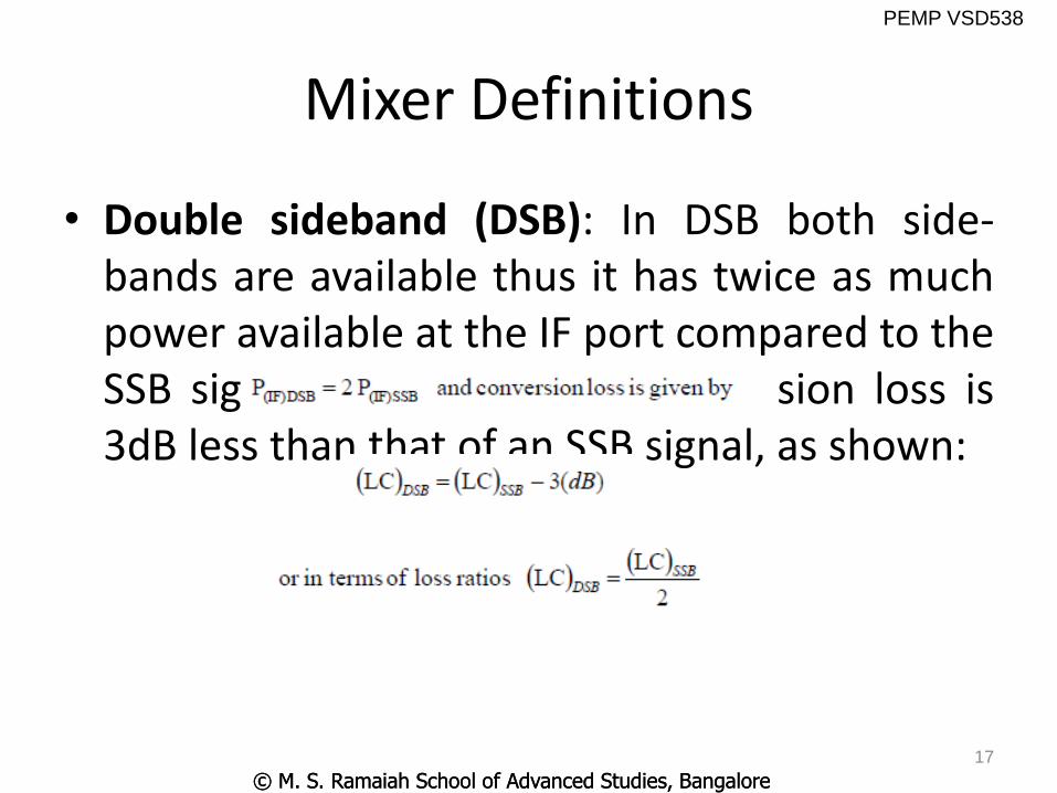
• Double sideband (DSB): In DSB both side-bands are available thus it has twice as muchpower available at the IF port compared to theSSB signal. As a result, it’s conversion loss is3dB less than that of an SSB signal, as shown:
17
© M. S. Ramaiah School of Advanced Studies, Bangalore
PEMP VSD538
© M. S. Ramaiah School of Advanced Studies, Bangalore
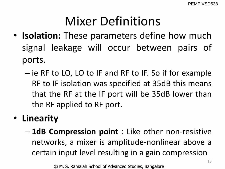
Mixer Definitions• Isolation: These parameters define how much
signal leakage will occur between pairs ofports.
– ie RF to LO, LO to IF and RF to IF. So if for exampleRF to IF isolation was specified at 35dB this meansthat the RF at the IF port will be 35dB lower thanthe RF applied to RF port.
• Linearity
– 1dB Compression point : Like other non-resistivenetworks, a mixer is amplitude-nonlinear above acertain input level resulting in a gain compression
18

© M. S. Ramaiah School of Advanced Studies, Bangalore
PEMP VSD538
© M. S. Ramaiah School of Advanced Studies, Bangalore
Gain Compression Characteristic
19

© M. S. Ramaiah School of Advanced Studies, Bangalore
PEMP VSD538
© M. S. Ramaiah School of Advanced Studies, Bangalore
1dB Compression point• Above this point the If fails to track the RF
input power level normally a 1dB rise in RFpower will result in a 1dB rise in the IF powerlevel. The 1dB compression point is measuredby plotting incident RF power against IF power
• 1dB compression point the input signal levelat which the output of the mixer has fallen1dB below the expected output level.
• For typical double balanced mixers this figureis ~ 6dB below the LO power level.
20

© M. S. Ramaiah School of Advanced Studies, Bangalore
PEMP VSD538
© M. S. Ramaiah School of Advanced Studies, Bangalore
Inter modulation (IM3)• Inter modulation: When two signals with different
frequencies are applied to a nonlinear system, the output ingeneral exhibits some components that are not harmonics ofthe input frequencies, called inter modulation (IM)
• It is measured by applying two closely spaced input tones atfrequencies F1 and F2.
• Third order products from the mixing of these tones with theLO (at frequency FLO) occur at frequencies given by:– (2F1 ± F2) ± FLO and (2F2 ± F1) ± FLO
• In the case of the mixer, the third order products of mostinterest are (2F1-F2)- FLO and (2F2-F1)-FLO as they fall in, or closeto the IF band.
21

© M. S. Ramaiah School of Advanced Studies, Bangalore
PEMP VSD538
© M. S. Ramaiah School of Advanced Studies, Bangalore
IM3 intercept point
• As a rule of thumb the IM3 intercept point is approximately 10dB above the 1dB compression point.
22
© M. S. Ramaiah School of Advanced Studies, Bangalore
PEMP VSD538
© M. S. Ramaiah School of Advanced Studies, Bangalore
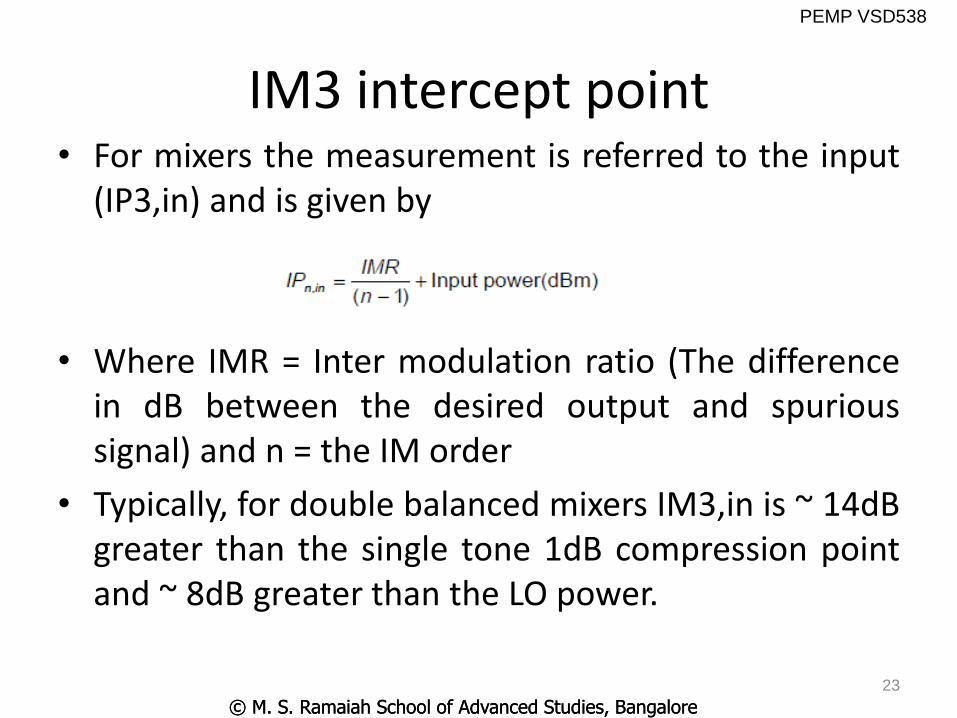
IM3 intercept point• For mixers the measurement is referred to the input
(IP3,in) and is given by
• Where IMR = Inter modulation ratio (The differencein dB between the desired output and spurioussignal) and n = the IM order
• Typically, for double balanced mixers IM3,in is ~ 14dBgreater than the single tone 1dB compression pointand ~ 8dB greater than the LO power.
23
© M. S. Ramaiah School of Advanced Studies, Bangalore
PEMP VSD538
© M. S. Ramaiah School of Advanced Studies, Bangalore
Balanced Architecture
24
© M. S. Ramaiah School of Advanced Studies, Bangalore
PEMP VSD538
© M. S. Ramaiah School of Advanced Studies, Bangalore
Image Rejection
25
Image Frequency: Frequencies with high PSD and close to RF such that the IF due
to RF generated is overshadowed by the IF due to image or frequencies that are
translated into the same IF band

© M. S. Ramaiah School of Advanced Studies, Bangalore
PEMP VSD538
© M. S. Ramaiah School of Advanced Studies, Bangalore
Image Reject Architectures
• A single stage mixer is susceptible to image distortions
corrupting the IF signal and making the detection of
signal difficult
• The concept of image rejection was realized out of dire
necessity
• Traditional mixers used a SAW bandpass filter for
image frequency rejection
• Image Rejection Mixers are useful particularly when
the desired and image are very close (low IF
frequencies) and a narrow-band channel pre-selector
(SAW) renders impracticable
26

© M. S. Ramaiah School of Advanced Studies, Bangalore
PEMP VSD538
© M. S. Ramaiah School of Advanced Studies, Bangalore
Image Reject Mixer
27
© M. S. Ramaiah School of Advanced Studies, Bangalore
PEMP VSD538
© M. S. Ramaiah School of Advanced Studies, Bangalore
Up / Down Conversion
28
© M. S. Ramaiah School of Advanced Studies, Bangalore
PEMP VSD538
© M. S. Ramaiah School of Advanced Studies, Bangalore
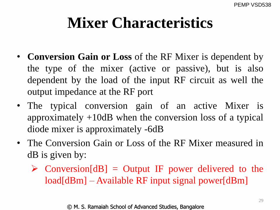
Mixer Characteristics
• Conversion Gain or Loss of the RF Mixer is dependent by
the type of the mixer (active or passive), but is also
dependent by the load of the input RF circuit as well the
output impedance at the RF port
• The typical conversion gain of an active Mixer is
approximately +10dB when the conversion loss of a typical
diode mixer is approximately -6dB
• The Conversion Gain or Loss of the RF Mixer measured in
dB is given by:
Conversion[dB] = Output IF power delivered to the
load[dBm] –Available RF input signal power[dBm]
29

© M. S. Ramaiah School of Advanced Studies, Bangalore
PEMP VSD538
© M. S. Ramaiah School of Advanced Studies, Bangalore
Mixer Characteristics
• Input Intercept Point (IIP3) is the RF input power at
which the output power levels of the unwanted
intermodulation products and the desired IF output
would be equal
• From an RF System point of view, a Mixer linearity is
more critical than Noise Figure
• The Third-Order intercept point (IP3) in a Mixer is
defined by the extrapolated intersection of the primary
IF response with the two-tone third-order
intermodulation IF product that results when two RF
signals are applied to the RF port of the Mixer
30

© M. S. Ramaiah School of Advanced Studies, Bangalore
PEMP VSD538
© M. S. Ramaiah School of Advanced Studies, Bangalore
IP3 (Intercept Point 3)
31
© M. S. Ramaiah School of Advanced Studies, Bangalore
PEMP VSD538
© M. S. Ramaiah School of Advanced Studies, Bangalore
Mixer Characteristics
• Isolation is the amount of local oscillator power that
leaks into either the IF or the RF ports
• There are multiple types of isolation: LO-to-RF, LO-
to-IF and RF-to-IF isolation
• Noise Figure is a measure of the noise added by the
Mixer itself, noise as it gets converted to the IF
output
• In a mixer noise is replicated and translated by each
harmonic of the LO that is referred to as Noise
Folding
32

© M. S. Ramaiah School of Advanced Studies, Bangalore
PEMP VSD538
© M. S. Ramaiah School of Advanced Studies, Bangalore
Diode Mixer
33
Single-device Mixer using one diode is primarily a process of matching the pumped
diode to the RF input and IF output, terminating the diode properly at LO harmonics and
unwanted mixing frequencies (other than the RF and IF), and isolating the RF, LO, and
IF ports
Isolation, and in some cases the termination, can be provided by using filters, a balanced
structure, or both
The choice depends on the frequency range and the intended application.

© M. S. Ramaiah School of Advanced Studies, Bangalore
PEMP VSD538
© M. S. Ramaiah School of Advanced Studies, Bangalore
Single Balanced Active Mixer
34
• This configuration
provides gain
• More noisy at higher
frequencies
• No isolation
• Simple and used low
end application

© M. S. Ramaiah School of Advanced Studies, Bangalore
PEMP VSD538
© M. S. Ramaiah School of Advanced Studies, Bangalore
Diode Double Balanced Mixer
• The local oscillator, LO,signal turns on first one arm(D3, D4), and then the other(D1, D2) within the diodering
• As the points where the LOsignal enters the diode ringat the junction of D1 and D4appear as a virtual earth tothe RF signal, this meansthat the points where the RFsignal enters are alternativelyconnected to ground as thediodes turn on and off
35

© M. S. Ramaiah School of Advanced Studies, Bangalore
PEMP VSD538
© M. S. Ramaiah School of Advanced Studies, Bangalore
Balanced Mixer Gilbert Cell
36
© M. S. Ramaiah School of Advanced Studies, Bangalore
PEMP VSD538
© M. S. Ramaiah School of Advanced Studies, Bangalore
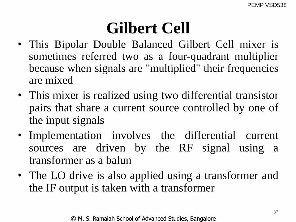
Gilbert Cell• This Bipolar Double Balanced Gilbert Cell mixer is
sometimes referred two as a four-quadrant multiplierbecause when signals are "multiplied" their frequenciesare mixed
• This mixer is realized using two differential transistorpairs that share a current source controlled by one ofthe input signals
• Implementation involves the differential currentsources are driven by the RF signal using atransformer as a balun
• The LO drive is also applied using a transformer andthe IF output is taken with a transformer
37
© M. S. Ramaiah School of Advanced Studies, Bangalore
PEMP VSD538
© M. S. Ramaiah School of Advanced Studies, Bangalore
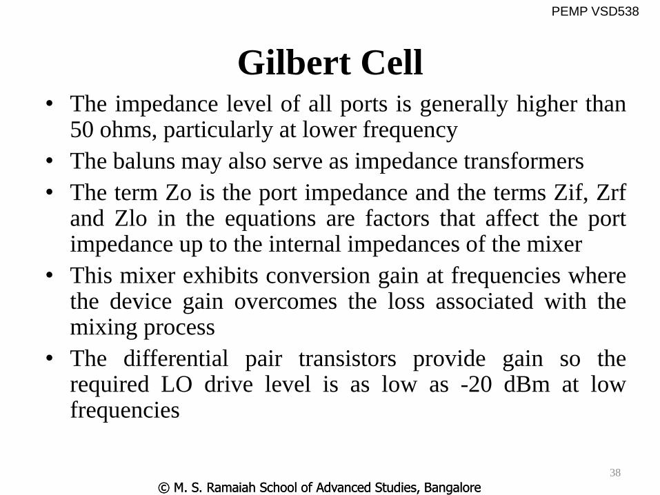
Gilbert Cell• The impedance level of all ports is generally higher than
50 ohms, particularly at lower frequency
• The baluns may also serve as impedance transformers
• The term Zo is the port impedance and the terms Zif, Zrfand Zlo in the equations are factors that affect the portimpedance up to the internal impedances of the mixer
• This mixer exhibits conversion gain at frequencies wherethe device gain overcomes the loss associated with themixing process
• The differential pair transistors provide gain so therequired LO drive level is as low as -20 dBm at lowfrequencies
38

© M. S. Ramaiah School of Advanced Studies, Bangalore
PEMP VSD538
© M. S. Ramaiah School of Advanced Studies, Bangalore
Image Reject Mixer Topologies
39
Hartley Architecture
Weaver Architecture

© M. S. Ramaiah School of Advanced Studies, Bangalore
PEMP VSD538
© M. S. Ramaiah School of Advanced Studies, Bangalore
Balun
• For the purposes of the simulation we need toconvert the differential inputs and outputs ofthe mixer to single ended source and loadimpedances. The device that achieves thisbalanced to un-balanced transformation isknown as a ‘Balun’.
40

© M. S. Ramaiah School of Advanced Studies, Bangalore
PEMP VSD538
© M. S. Ramaiah School of Advanced Studies, Bangalore
Test setup
41

© M. S. Ramaiah School of Advanced Studies, Bangalore
PEMP VSD538
© M. S. Ramaiah School of Advanced Studies, Bangalore
Inputs to mixer• As the inputs and outputs are differential balun
trans-formers have been added to convert to singleended inputs and outputs.
• The 500-ohm load Term3 correctly terminates themixer 500-ohm output impedance.
• The RF frequency is set to 2500MHz (RF_freq), Localoscillator frequency to 2250MHz (LO_freq) , resultingin an IF frequency of 250MHz (IF_Freq)..
• For correct switching of the LO transistors thevariable vg needs to be set to 1V – running thesimulation this gives Vgs across the switchingtransistor of ~ 1V. 42

© M. S. Ramaiah School of Advanced Studies, Bangalore
PEMP VSD538
© M. S. Ramaiah School of Advanced Studies, Bangalore
Simulation Results
43

© M. S. Ramaiah School of Advanced Studies, Bangalore
PEMP VSD538
© M. S. Ramaiah School of Advanced Studies, Bangalore
Simulation Results
44

© M. S. Ramaiah School of Advanced Studies, Bangalore
PEMP VSD538
© M. S. Ramaiah School of Advanced Studies, Bangalore
Simulation Results
45

© M. S. Ramaiah School of Advanced Studies, Bangalore
PEMP VSD538
© M. S. Ramaiah School of Advanced Studies, Bangalore
Simulation Results
46

© M. S. Ramaiah School of Advanced Studies, Bangalore
PEMP VSD538
© M. S. Ramaiah School of Advanced Studies, Bangalore
Summary• RF/MW mixers and Oscillators are the important building
blocks in any RF system
• Mixers are classified in to Unbalanced Mixer & Balanced
Mixer depending on the input phase
• Image Reject Architectures has been described as class of
mixers which can combat image frequencies
47

∗∗∗∗ Liam Devlin is with Plextek Communications Technology Consultants, London Road, Great Chesterford, Essex, CB10 1NY Tel: +44 (0)1799 533200 Fax: +44 (0)1799 533201 Email: [email protected]
Mixers Liam Devlin
∗∗∗∗
1. Introduction Mixers are frequency translation devices. They allow the conversion of signals between a high frequency (the RF frequency) and a lower Intermediate Frequency (IF) or baseband. In communications systems the RF is the transmission frequency, which is converted to an IF to allow improved selectivity (filtering) and an easier implementation of low noise and high gain amplification. This paper details the design of mixer circuits, concentrating on low cost Printed Circuit Board (PCB) based designs using discrete Surface Mount Technology (SMT) components.
2. The Fundamentals The non-linear behaviour of a mixing device is used to realise the mixing function. Diodes, Field Effect Transistors (FETs) and bipolar transistors can all be used as mixers and are all covered in this paper. Figure 1 shows the typical I-V characteristics of a Schottky diode, which can be described by equation (1).
.........44
33
221 ++++= VaVaVaVaI (1)
I (mA)
0
25
50
75
100
125
150
0 0.25 0.5 0.75 1 1.25 1.5
Vf (volts)
Figure 1: Typical forward I-V Characteristics of a diode
If the diode is excited by two sinusoids, Cos(ω1t) and Cos(ω2t) the current through the diode is given by equation (2).
....))()(())()(( 2212211 ++++= tCostCosatCostCosaI ωωωω (2)
When expanded this contains the term 2a2Cos(ω1t)Cos(ω2t) which has the trigonometrical relationship shown in (3). It is either the sum or difference term that is the desired output of a mixer.
))(())(()()(2 212121 tCostCostCostCos ωωωωωω ++−= (3)

Diodes are “square-law” devices, which means the function describing their non-linear behaviour has a strong a2 component. This means that if excited correctly they should be able to produce a strong mixing product. Thus the basic mixer design entails injecting the signals to be mixed and extracting the desired mixing product whilst maximising the efficiency of the conversion. One significant problem with mixers is that in addition to the wanted product, there are also numerous unwanted spurious products, often referred to as “spurs”. Figure 2 depicts the spectral output of a downconverting mixer. The Local Oscillator (LO) is mixed with the wanted RF signal to produce a copy of the RF signal at the difference frequency (the IF). In general the mixer will generate outputs at a range of frequencies given by mRF ± nLO. The spectrum shown in Figure 2 has an LO frequency below the IF, this is known as low-side injection.
One frequency of particular importance is the image frequency. This is 2IF away from the RF and will be converted directly to the same IF frequency as the RF. Noise and unwanted signals present at this frequency can severely degrade the system performance. Filtering and/or image reject mixers (covered later in this paper) are normally incorporated to address this problem. More detailed information on the system design can be found in [1]. In the case of upconverting mixers the input signal is the IF and the desired output signal is either the product or difference of the LO and IF frequencies, depending whether high-side or low-side injection is being used. If the wanted output is LO+IF, the difference product (LO-IF) is termed the unwanted side-band, or image and must be rejected by filtering or the use of an image-reject mixer. Most mixers incorporate some form of filtering which helps to reduce the levels of the unwanted spurious outputs. Another commonly used technique, which helps reduce spurious outputs, is the use of balanced mixer designs. More detail on balanced mixer design is included in Section 4.
3. Mixer Terminologies Listed below are some of the terms used in referring to mixers or mixing performance: Conversion loss: The ratio of the wanted output signal level to the input, normally expressed in dB. Noise Figure: The ratio of the Signal to Noise Ratio (SNR) at the input compared to the SNR at the output, measured at 290K. To avoid ambiguity this paper will use the term noise figure to refer to the value of this ratio in dB and the term noise factor to refer to the value as an absolute ratio.
Double Sideband (DSB) Noise Figure: Includes noise and signal contributions at both the RF and the image frequencies. Single Sideband (SSB) Noise Figure: No image signal is included although image noise is included. Provided the mixer performance is the same at the image and the wanted frequencies, the SSB noise factor = twice the DSB noise factor.
Compression: For small input signal levels, each dB increase in signal level results in a dB increase in the output signal level. As the input signal level continues to increase, the conversion loss of the mixer will
LO
RF
IF(RF-LO)
2LO 2RF
Image(LO-IF)
2IF
3IF2RF-LO
Figure 2: Mixer spectral output

eventually start to increase. The 1dB compression point is the input signal level at which the conversion loss has increased by 1dB. Mixers should be used “backed-off” from the 1dB compression point as in addition to distortion of the wanted signal, operation at or close to it would give rise to significant increases in the levels of the spurious outputs. Third Order Intercept Point. This is a figure of merit to give an indication of the mixer’s signal handling capability. In particular it provides an indication of the levels of third order products a mixer is likely to produce under multi-tone excitation. It is measured by applying two closely spaced input tones at frequencies F1
and F2. Third order products from the mixing of these tones with the LO (at frequency FLO) occur at frequencies given by: (2F1±F2)±FLO and (2F2±F1)±FLO. In the case of a downconvert mixer, the third order products of most interest are (2F1-F2)-FLO and (2F2-F1)-FLO as they fall in, or close to the IF band. Figure 3 depicts the IF output spectrum of a downconvert mixer under two-tone excitation.
The third order intercept point itself is an entirely imaginary point, at which the third order product becomes as
large as the direct downconverted product. The level of the third order products rises at three times the rate of increase of the input signal level and fundamental output level. The mixer’s output referred third order intercept point (TOIout) is given by equation (4), all values are in dB and it is the dB value of ∆L which is divided by 2.
2
LPTOI IFout
∆+= (4)
With mixers, the third order intercept point is often referred to the input, which just requires adding the conversion loss to TOIout. Linearity. The linearity of a mixer refers to its signal level handling ability. Thus a mixer with high linearity will have a high TOI. Spur’s. An abbreviation of spurious product. The term is used to describe any unwanted mixing product. Sub-harmonic mixer. This is a mixer circuit designed to accept an LO input at a fraction (often a half) of the desired LO mixing frequency. Harmonic mixer. This is just another term for sub-harmonic mixer but is more commonly used for circuits employing higher multiples of the input LO to produce the mixing LO. Pump. A term sometimes used to describe the LO drive. The LO input is said to be “pumping” the mixer. Image frequency. For high side injection (FLO > FRF) this is FLO + FIF, for low side injection (FLO < FRF) it is FLO - FIF. In downconvert mixers, it is a frequency that is converted directly to IF along with the IF itself. In upconvert mixers it is an unwanted sideband which, without additional filtering, is usually at a similar level to the wanted signal.
(2F1-F2)-FLO(2F2-F1)-FLO
F1-FLOF2-FLO
∆∆∆∆L
PIF
Figure 3: IF spectrum for mixer third order intercept
point measurement

Image-reject mixers. A more complex mixer configuration, which has the advantage of providing inherent cancellation of the image signal. Image enhancement. A method for reducing the conversion loss of a mixer by terminating the image frequency in an appropriate reactive impedance. Should be used with caution as the resultant mixer can have severely degraded intermodulation performance [5]. Also, the exact image impedance is normally found empirically.
4. Diode Mixers Most modern diode mixer designs use Schottky diodes. The main reason for this is that the Schottky diode is a majority carrier device which means it has a higher switching speed than p-n junction diodes [2]. In-expensive plastic packaged diodes are now available, which are suitable for designing mixers up to around 13GHz. Manufactures normally specify the intended application of a particular diode and the selection of a suitable diode is a vital step in diode mixer design. It is also common for manufacturers to refer to diodes as low, medium or high barrier. The higher the barrier height, the higher the forward voltage required to turn the diode on. The exact definition of what constitutes a low, medium or high barrier is open to the manufacturer’s interpretation. However, broadly speaking, for a forward current of 1mA, low barrier diodes require a forward voltage of around 0.2 - 0.3V, medium 0.4 - 0.5V and high 0.6 - 0.7V. The higher the barrier, the higher the LO drive which will be required to obtain low loss mixing but the resultant mixer should have greater linearity. The electrical equivalent circuit for a packaged Schottky diode is shown in Figure 4. Also shown in Figure 4 is a typical RF Schottky diode in a SOT23 package; with a pencil tip for size comparison, Lp and Cp are the packaging parasitics. Rs is the parasitic series resistance of the diode and Cj and Rj are the non-linear components of the Schottky diode junction. The non-linearity of Rj is responsible for the square law behaviour of the diodes DC characteristics (Figure 1).
C j(V) Rj(V)
Rs
Lp
Cp
Figure 4: Equivalent circuit of a packaged Schottky diode and a photograph of a SOT23
packaged diode, with pencil tip for size reference
Most diode mixer designs utilise unbiased diodes, however forward biasing of the diodes, so a small DC current flows, can offer reduced conversion losses. This is particularly the case when limited LO drive is available. The diode is biased to have a quiescent operating point close to the region of maximum non-linearity in its operating characteristics which allows the diodes square law characteristic to be traversed with lower levels of LO drive.

4.1. Single-ended Diode Mixers Mixers, which utilise a single diode as the mixing element, have no inherent isolation between the mixer ports and are known as single-ended designs. Figure 5 shows a basic block diagram of a single-ended mixer.
One of the main difficulties with single-ended designs is that the LO and RF inputs must be separated with a diplexer filter. They are normally relatively closely spaced and separating the two frequency bands can be problematic. Coupled with this, the fact that no inherent spurious suppression is afforded by this topology, it is not surprising that few modern diode mixer designs are single-ended. The exception to this is high mm-wave frequency designs, which are still often realised with a single diode.
A step-by-step procedure for designing a single ended mixer is given below:
1. Choose a suitable diode for the application. Factors effecting this choice include operating frequency, available LO drive, cost versus performance trade-offs and package style.
2. Design the IF filter, the techniques described in [3] can be used. In addition to having low insertion loss it is important that it presents a high input impedance at the LO and RF frequency's. See also the comments on matching, below.
3. Design the RF and LO filters [3], in addition to having low loss and providing a diplexing action which gives isolation between the two inputs, the common output of these filters must provide a high impedance across the IF frequency band. See also the comments on matching, below.
4. Large signal simulators are now commonly available and most manufacturers supply large signal models for their diodes. It is strongly recommended that, when possible, a large signal analysis of the mixer be carried out prior to fabrication.
Matching: If a diode is considered as a switch, being either open or short-circuit, then impedance matching between the mixer ports and the diode is not possible and indeed not necessary. However, it is more appropriate to think of a mixer diode as a square-law device. The impedance that the diode presents is a time varying impedance, dependent on the LO level and frequency. It is the time-averaged value of the diode’s impedance, which must be used if matching is attempted. If an accurate large signal model and the packaging parasitics are available, simulation of the LO-dependant diode impedance is possible. For those without access to a large-signal simulator an estimate of the time-averaged value of Rj(V) and Cj(V) can be made. Matching to the diode can improve the performance of a mixer but it must be addressed with care. It is important to note that the filter requirements detailed in steps 2 and 3, above must still be satisfied with any matching networks present. Linearity: The best way to improve the linearity of a diode mixer is to increase the LO drive level. Higher barrier-height diodes should be used for best performance, provided that adequate LO drive is available. Techniques such as image-enhancement should be avoided as this can degrade linearity [5].
4.2. Single-balanced Diode Mixers A single-balanced diode mixer uses two diodes. Either the LO drive or the RF signal is balanced (applied in anti-phase), adding destructively at the IF port of the mixer and providing inherent rejection. The level of rejection is dependent on the amplitude and phase balance of the balun, providing the balanced drive, and the matching between the two diodes. A rejection of 20 to 30dB is normally possible for good discrete designs. Other advantages of a singly-balanced design are rejection certain mixer spurious products, depending on the exact configuration, and suppression of Amplitude Modulated (AM) LO noise. AM noise could be a significant
R F
LO
IF
Figure 5: Basic block diagram of a single-ended
mixer
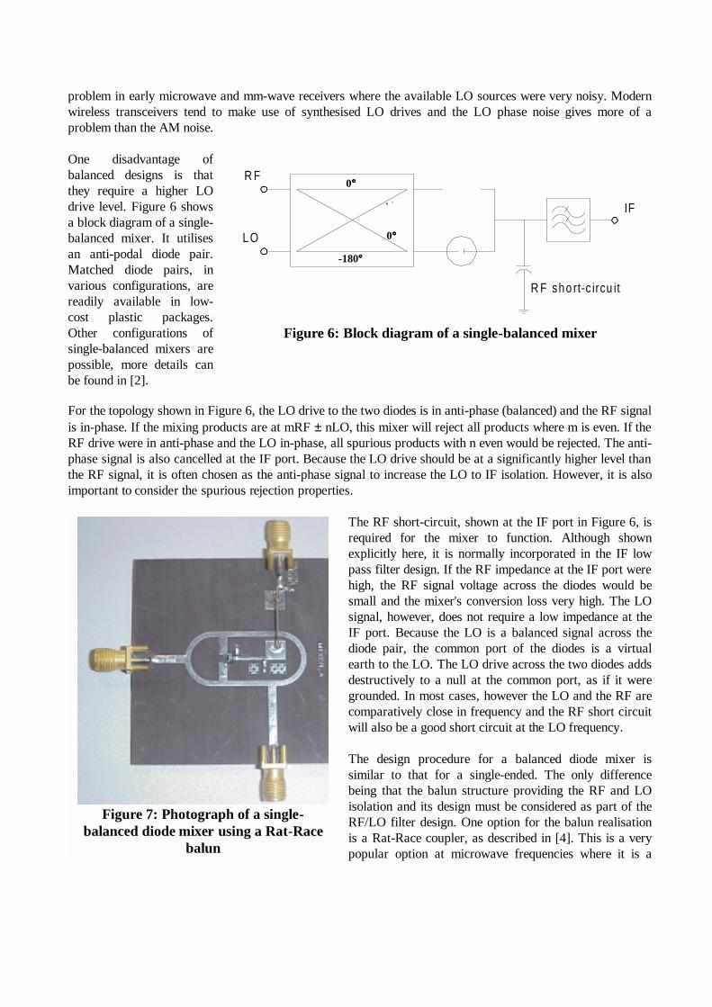
problem in early microwave and mm-wave receivers where the available LO sources were very noisy. Modern wireless transceivers tend to make use of synthesised LO drives and the LO phase noise gives more of a problem than the AM noise. One disadvantage of balanced designs is that they require a higher LO drive level. Figure 6 shows a block diagram of a single-balanced mixer. It utilises an anti-podal diode pair. Matched diode pairs, in various configurations, are readily available in low-cost plastic packages. Other configurations of single-balanced mixers are possible, more details can be found in [2]. For the topology shown in Figure 6, the LO drive to the two diodes is in anti-phase (balanced) and the RF signal is in-phase. If the mixing products are at mRF ± nLO, this mixer will reject all products where m is even. If the RF drive were in anti-phase and the LO in-phase, all spurious products with n even would be rejected. The anti-phase signal is also cancelled at the IF port. Because the LO drive should be at a significantly higher level than the RF signal, it is often chosen as the anti-phase signal to increase the LO to IF isolation. However, it is also important to consider the spurious rejection properties.
The RF short-circuit, shown at the IF port in Figure 6, is required for the mixer to function. Although shown explicitly here, it is normally incorporated in the IF low pass filter design. If the RF impedance at the IF port were high, the RF signal voltage across the diodes would be small and the mixer's conversion loss very high. The LO signal, however, does not require a low impedance at the IF port. Because the LO is a balanced signal across the diode pair, the common port of the diodes is a virtual earth to the LO. The LO drive across the two diodes adds destructively to a null at the common port, as if it were grounded. In most cases, however the LO and the RF are comparatively close in frequency and the RF short circuit will also be a good short circuit at the LO frequency. The design procedure for a balanced diode mixer is similar to that for a single-ended. The only difference being that the balun structure providing the RF and LO isolation and its design must be considered as part of the RF/LO filter design. One option for the balun realisation is a Rat-Race coupler, as described in [4]. This is a very popular option at microwave frequencies where it is a
0 °
0°°°°
0°°°°
-180°°°°
R F
L O
IF
R F sho rt-c ircu it
Figure 6: Block diagram of a single-balanced mixer
Figure 7: Photograph of a single-
balanced diode mixer using a Rat-Race balun

comparatively small structure that can be produced inexpensively on a printed substrate. Figure 7 shows a photograph of a prototype realisation of such a mixer. It covers the HIPERLAN RF band of 5.15 to 5.35GHz with a 700MHz IF, measured conversion loss is 7dB and the input referred 1dB compression point is +5dBm for an LO drive level of +8dBm. A SOT-23 packaged anti-podal diode pair has been used and a 1pF 0603 capacitor is used to realise the RF short at the IF port, whilst forming the first element of the IF low-pass filter. Figure 8 shows a 1.5GHz single-balanced mixer realised on an FR4 substrate with a lumped element balun. This had a conversion loss of 9dB for an LO drive of +8dBm. The ceramic resonator filter to the bottom left of Figure 8 is the RF image filter. At the output of this filter is the lumped element RF filter of the mixer. It connects to the common port of the antipodal diode pair (in the SOT23 package). The IF port of the mixer (at the top centre of Figure 8) is also connected to the common port of the diode pair via a filter. The output of the RF filter needs to present an open circuit to the output of the IF filter and vice-versa. The LO input is to the bottom right and a simple lumped element balun providing a differential drive across the diode pair.
4.3. Double-balanced Diode Mixers A double-balanced diode mixer normally make use of four diodes in a ring or star configuration with both the LO and RF being balanced. All ports of the mixer are inherently isolated from each other. Matched diode rings (fabricated in close proximity on the same substrate material) are readily available in SOT143 plastic packages. The advantages of a double-balanced design over a single balanced design are increased linearity, improved suppression of spurious products (all even order products of the LO and/or the RF are suppressed) ant the inherent isolation between all ports. The disadvantages are that they require a higher level LO drive and require two baluns. Figure 9 shows a block diagram of a double-balanced quad-ring diode mixer. Details of the star topology can be found in [2]. The operation of a double balanced mixer is best understood by considering the diodes as switches. The LO alternately turns the right hand pair and left hand pair of diodes on and off in anti-phase. Points ‘a’ and ‘c’ are virtual earths to the RF signal and can be considered as connected to ground. Thus points ‘b’ and ‘d’ (the balanced RF signal) are alternately connected to ground (at points ‘a’ and ‘c’). This means an in-phase RF signal and an anti-phase RF signal are alternately routed to the IF port under control of the LO. Thus the signal at the IF port is effectively the RF signal multiplied by an LO square wave of peak magnitude ±1.
Figure 8: Photograph of a single-balanced
mixer with lumped element balun
IF
R F
LO
a
b
c
d
Figure 9: Block diagram of a double-balanced
diode mixer

This action is easily demonstrated using simple mathematical processing software. Figure 10 shows a sinusoidal voltage waveform at a frequency of 1GHz, this is the RF waveform. Figure 11 shows a square wave at a frequency of 870MHz, this is the LO switching waveform. Multiplication of the two will produce a waveform wit a strong component at the difference frequency (IF) of 130MHz.
0 5 10 15 20
1
0
1
Vrfn
tn
Figure 10: RF voltage waveform versus time in ns
0 5 10 15 20
1
0
1
Vlon
tn
Figure 11: LO voltage waveform versus time in ns
Figure 12 shows the result of multiplying the RF and LO waveforms. A low frequency sinusoid is clearly visible. This is a replica of the RF signal (i.e. a sinusoid) translated to the IF frequency of 130MHz. Although this method of mixer analysis provides a qualitative understanding of how the mixer functions, it is not adequate to predict the RF functionality. Ideal square wave multiplication, such as this, results in a conversion loss of 3.9dB. In practice diode-ring mixers have additional losses (in the baluns and diodes) and imperfections which increase the conversion loss actually achieved. A loss of between 6 and 8dB is typical for a
0 5 10 15 20 25 30 35 40
1
0
1
Vifn
tn
Figure 12: IF voltage waveform (Vrf*Vlo) versus time in ns
well designed diode ring mixer. In order to predict accurately the mixer’s performance, large signal circuit simulation must be performed. The block diagram in Figure 9 shows the differential RF and LO signals provided using wire-wound ferrite transformers. Wire-wound transformers can be used at frequencies up to over 2GHz but lower cost printed or lumped element baluns are often implemented in practical mixers. At higher frequencies wire wound transformers become impractical and printed and/or lumped baluns become the norm. Care should be taken to consider how the performance of these baluns differs from wound transformers; additional filtering may be necessary. An overview of practical balun configurations is given in Section 5.
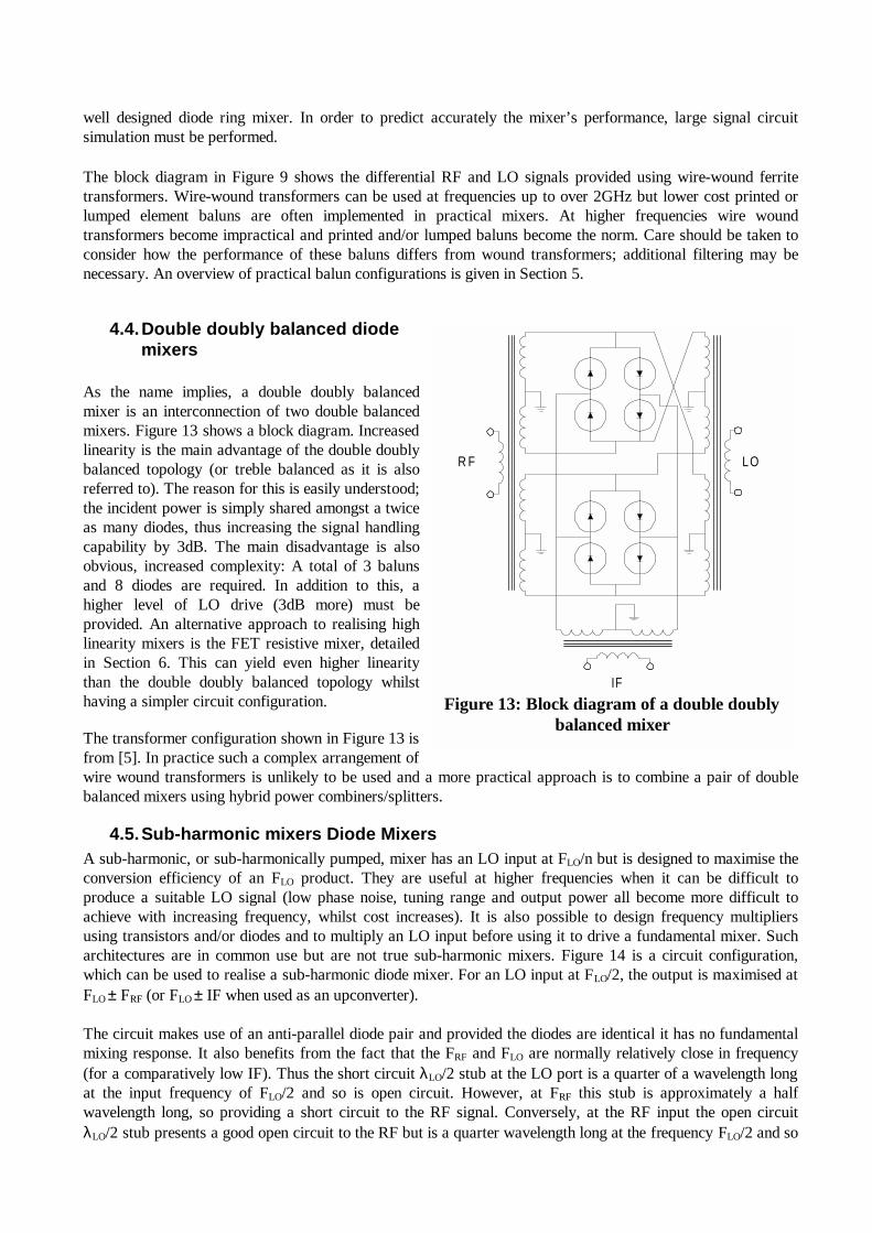
4.4. Double doubly balanced diode mixers
As the name implies, a double doubly balanced mixer is an interconnection of two double balanced mixers. Figure 13 shows a block diagram. Increased linearity is the main advantage of the double doubly balanced topology (or treble balanced as it is also referred to). The reason for this is easily understood; the incident power is simply shared amongst a twice as many diodes, thus increasing the signal handling capability by 3dB. The main disadvantage is also obvious, increased complexity: A total of 3 baluns and 8 diodes are required. In addition to this, a higher level of LO drive (3dB more) must be provided. An alternative approach to realising high linearity mixers is the FET resistive mixer, detailed in Section 6. This can yield even higher linearity than the double doubly balanced topology whilst having a simpler circuit configuration. The transformer configuration shown in Figure 13 is from [5]. In practice such a complex arrangement of wire wound transformers is unlikely to be used and a more practical approach is to combine a pair of double balanced mixers using hybrid power combiners/splitters.
4.5. Sub-harmonic mixers Diode Mixers A sub-harmonic, or sub-harmonically pumped, mixer has an LO input at FLO/n but is designed to maximise the conversion efficiency of an FLO product. They are useful at higher frequencies when it can be difficult to produce a suitable LO signal (low phase noise, tuning range and output power all become more difficult to achieve with increasing frequency, whilst cost increases). It is also possible to design frequency multipliers using transistors and/or diodes and to multiply an LO input before using it to drive a fundamental mixer. Such architectures are in common use but are not true sub-harmonic mixers. Figure 14 is a circuit configuration, which can be used to realise a sub-harmonic diode mixer. For an LO input at FLO/2, the output is maximised at FLO ± FRF (or FLO ± IF when used as an upconverter). The circuit makes use of an anti-parallel diode pair and provided the diodes are identical it has no fundamental mixing response. It also benefits from the fact that the FRF and FLO are normally relatively close in frequency (for a comparatively low IF). Thus the short circuit λLO/2 stub at the LO port is a quarter of a wavelength long at the input frequency of FLO/2 and so is open circuit. However, at FRF this stub is approximately a half wavelength long, so providing a short circuit to the RF signal. Conversely, at the RF input the open circuit λLO/2 stub presents a good open circuit to the RF but is a quarter wavelength long at the frequency FLO/2 and so
IF
LOR F
Figure 13: Block diagram of a double doubly
balanced mixer

is short circuit. The IF is normally far enough away from the RF frequency to allow easy realisation of an IF filter presenting an open circuit output to the RF port.
RF
LO/2IF
λLO
/2λLO/2
Figure 14: Block diagram of a sub-harmonic diode mixer
A photograph showing a practical implementation of this type of sub-harmonic mixer is shown in Figure 15. It uses an antiparallel diode pair in a low cost SOT 23 package. The IF port is to the left, going into a low pass filter ending in an 0402 chip inductor which is open circuit resonant at the RF frequency of 11.7 to 12.7GHz. The IF frequency is 1 to 2GHz and the FLO/2 input is fixed at 5.35GHz (FLO=10.7GHz).
Figure 15: Photograph of a 12GHz sub-harmonically pumped mixer
The conversion loss versus RF frequency has been measured for this mixer at three LO input power levels (+5dBm, +8dBm and +10dBm), a graph of the results is shown in Figure 16. For LO drive levels of 8 or 10dBm the conversion loss is between 9.5 and 11dB, which is only slightly more than would have been achieved
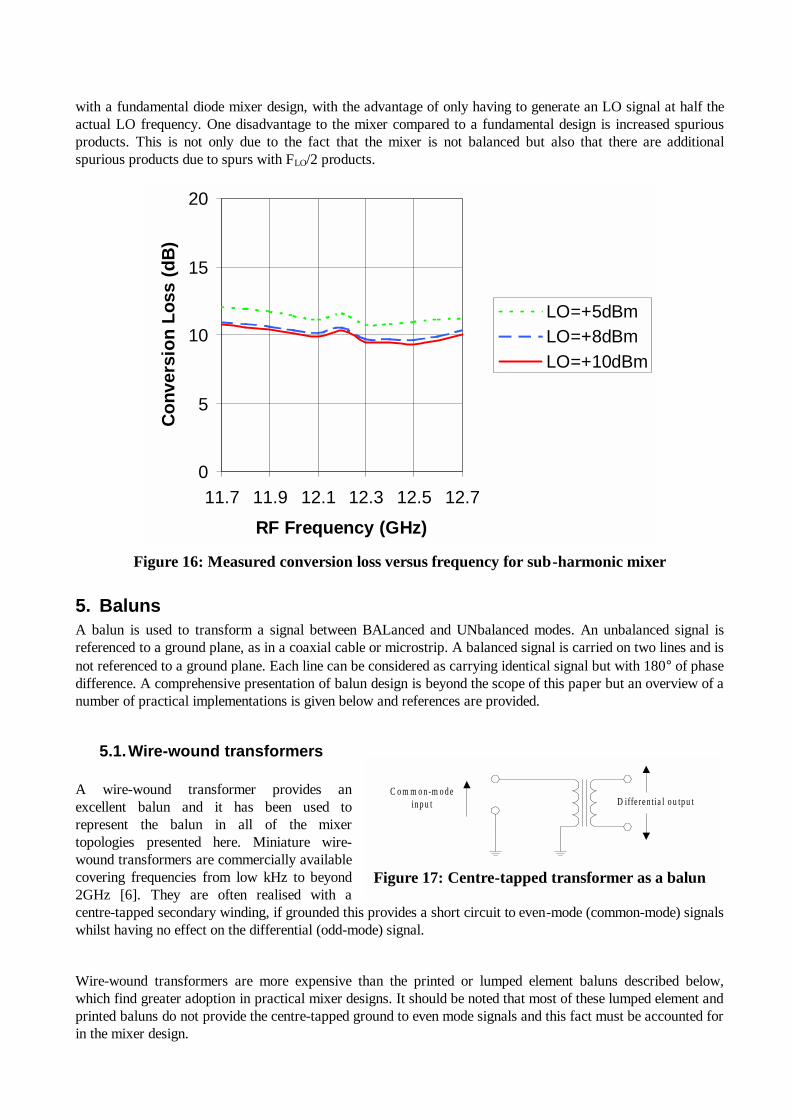
with a fundamental diode mixer design, with the advantage of only having to generate an LO signal at half the actual LO frequency. One disadvantage to the mixer compared to a fundamental design is increased spurious products. This is not only due to the fact that the mixer is not balanced but also that there are additional spurious products due to spurs with FLO/2 products.
0
5
10
15
20
11.7 11.9 12.1 12.3 12.5 12.7
RF Frequency (GHz)
Co
nver
sio
n L
oss
(dB
)
LO=+5dBmLO=+8dBmLO=+10dBm
Figure 16: Measured conversion loss versus frequency for sub-harmonic mixer
5. Baluns A balun is used to transform a signal between BALanced and UNbalanced modes. An unbalanced signal is referenced to a ground plane, as in a coaxial cable or microstrip. A balanced signal is carried on two lines and is not referenced to a ground plane. Each line can be considered as carrying identical signal but with 180° of phase difference. A comprehensive presentation of balun design is beyond the scope of this paper but an overview of a number of practical implementations is given below and references are provided.
5.1. Wire-wound transformers A wire-wound transformer provides an excellent balun and it has been used to represent the balun in all of the mixer topologies presented here. Miniature wire-wound transformers are commercially available covering frequencies from low kHz to beyond 2GHz [6]. They are often realised with a centre-tapped secondary winding, if grounded this provides a short circuit to even-mode (common-mode) signals whilst having no effect on the differential (odd-mode) signal.
Wire-wound transformers are more expensive than the printed or lumped element baluns described below, which find greater adoption in practical mixer designs. It should be noted that most of these lumped element and printed baluns do not provide the centre-tapped ground to even mode signals and this fact must be accounted for in the mixer design.
C o m m o n -m o d ein p u t D iffe ren tia l o u tp u t
Figure 17: Centre-tapped transformer as a balun

5.2. Printed baluns There are a wide range of printed balun topologies [7] they have the advantage of being inexpensive, realised as they are on the Printed Circuit Board (PCB) or Microwave Integrated Circuit (MIC) substrate. On the downside they can be quite large, particularly at lower RF frequencies. The rat-race coupler shown in Section 4.1 is commonly used at microwave frequencies for bandwidths of up to around 10-20%.
Possibly the simplest printed balun is the coupled line balun [8], also called a parallel-line balun shown in Figure 18. The structure is a quarter of a wavelength long at the centre frequency. It is capable of bandwidths of over an octave, provided the coupling between the lines is high enough. In practice this is not normally the case for the simple edge coupled balun shown in Figure 18. A more practical approach is to
use multiple coupled lines as shown in Figure 19 or, where multi-layer substrate processing is available, to adopt a broad-side coupler topology as in Figure 20. This broadside-coupled implementation is often referred to as a parallel plate balun.
C o m m o n -m o d ein p u t
D iffe ren tia l o u tp u t
Figure 20: Coupled line balun, using broadside coupler structure
An improvement on the parallel-line balun is a printed version of the “Marchand Balun”. This is derived from the co-axial balun, described by Nathan Marchand in 1944 [9]. The printed version of the Marchand balun is shown in its simplest form in Figure 21. This is more tolerant to low even mode impedance (low coupling ratio) than the parallel line balun and has a wider bandwidth.
C o m m o n-m o d ein pu t
D iffe ren tia l o u tp u t
O penC ircu it
C o m m o n -m o d ein p u t
D iffe ren tia l o u tp u t
Figure 18: Simple coupled line balun
D iffe ren tia l o
C o m m o n -m o d ein p u t
Figure 19: Coupled line balun using multiple coupled lines

Figure 21: Printed Marchand Balun
As with the parallel line balun, improved performance is obtained if multiple planar section are used [10] or if a broadside coupling topology is adopted [11]. One draw back to using these printed baluns at lower RF frequencies is their size. One technique to reducing the size is to include lumped elements and printed structures, as shown in Figure 22. This allows acceptable balun performance to be achieved with significant area reduction [12]. As with the parallel line and Marchand baluns, the use of broadside, rather than edge, coupling will yield tighter coupling and improved performance.
5.3. Lumped Element Baluns Lumped element baluns are based around the fact that the insertion phase through a low pass filter lags the insertion phase through a high pass filter [13]. It therefore possible to design low pass and high pass filters that have a relatively constant 180° difference in insertion phase. A wide range of topologies is possible and for narrow band designs, very simple structures can be adequate [14]. Figure 23 shows a lumped element implementation of a rat-race splitter/combiner [7]. Signals incident on the Σ port split equally in amplitude and phase, whilst signals incident on the ∆ port split equally in phase but have a 180° phase difference. Design equations are shown in the figure, Zo is t he system impedance.
CC
C C
2C 2C
L
LL
In /O u t1
In /O u t2 ∆
Σ
oo
o ZC
L 21
==ω
ω
Figure 23: Lumped element realisation of a rat-race splitter
5.4. Active Baluns Active baluns have a number of disadvantages:
• Degraded intermodulation performance for the resultant mixer • Amplitude and phase balance is normally poorer than for passive designs • Discrete realisations sensitive to package parasitics
D iffe ren tia l o u tp u t
C o m m o n -m o d ein p u t
Figure 22: Reduced size printed
balun

• DC bias is required • The output impedances of each port can be significantly different
Figure 24 shows three possible active balun realisations.
3 -p or t p h ase sp l itter C -B /C -E a m p li fier L on g -ta il p a i r
Figure 24: Active balun topologies
The 3-port phase splitter only really works well at lower frequencies but can be quite compact. The C-B/C-E balun can work well over quite wide bandwidths provided parasitics are well modelled. The long-tail pair is commonly used in integrated realisations, closer inspection will reveal it is extremely similar in architecture to the C-B/C-E topology.
6. FET Mixers FETs can be used in mixers in both active and passive modes. Active FET mixers are transconductance mixers using the LO signal to vary the transconductance of the transistor. They have the advantage of providing the possibility of conversion gain rather than loss and can also have lower noise figures than passive designs. Figure 25 shows the simplest realisation of a transconductance mixer, biasing circuitry has been omitted for clarity. The RF (and LO) short circuit at the drain is important to ensure that the value of Vds is not moved significantly from its DC bias point by the applied LO. This ensures the magnitude of the time varying transconductance is maximised so optimising the conversion gain. Unfortunately it also means that this mixer topology is not well suited to realising upconverters. The topology of Figure 25 has the disadvantage that some form of diplexing is required to separate the RF and LO inputs which are incident on the same port. For this reason dual gate FET mixers are often used. This toplogy is essentially a cascode arrangement of two transistors as shown in Figure 26, although in practice four terminal dual gate FET devices are sometimes used.
IF O utput
R F short-circu it
R F and LOInput
Figure 25: Simple transconductance mixer

The RF input is applied to the bottom device which is matched using the well-known techniques developed for amplifier design, the LO signal is applied to the top device, which is often resistively matched. One advantage
this structure has is that the LO and RF signals are inherently isolated. It can be used to develop compact mixers with conversion gain, as described in [15]. Although the potential of conversion gain rather than loss, which the transconductance mixer offers, is attractive the downside is that they tend to have lower linearity than passive designs. When used in passive mode, the FET is used as a switch. Its suitability for switch realisation
stems from the fact that its drain-source resistance behaves as a voltage variable resistor, the resistance being set by the gate-source voltage [16]. When used as a switch, a FET is operated with the drain and source at zero volts DC. The RF signal path is drain to source and the gate is the control terminal. It can be represented by the simplified equivalent circuit shown in Figure 27.
Rg
Vg
Figure 27: Simplified equivalent circuit of a passive switching FET
A simple FET switching mixer, which can provide high linearity for moderate LO drive levels, is shown in Figure 28. The gates of the FETs are biased part way between 0V and pinch off, this allows the LO signal to move the FETs between their “on” and “off” states. At lower RF frequencies FET gates have a high input impedance and the load for the differential LO signal is thus approximately 2Rg (Figure 28). By setting Rg to a moderately high value say (200 or 300Ω), increased gate voltage swing can be obtained for the same LO level as compared to driving a 100Ω differential load. At higher frequencies, the input capacitance of the FET gate presents a lower reactance and the LO voltage swing will be reduced for the same LO power level. FET switching mixers will not function well if the gates are left unbiased. If the LO signal is large enough to turn the FETs “off” on the negative cycle, it will drive the gate-source junction in to forward bias on the positive cycle. It is vital that the gate bias voltage is set appropriately if optimum mixer performance is to be obtained. For discrete implementations this gives a problem as the specified range of pinch-off voltages for the FETs can be very wide (-0.5V to –2.5V is a typical range). Whilst integrated designs can overcome this problem with on-chip bias circuitry, for discrete designs there are two solutions: Select on test resistors can be used to set the bias or a supply of FETs with a reduced range of pinch-off voltages can be agreed with the manufacturer. Both solutions have cost penalties.
IF O u tp u t
R F sho rt-c ircu itR F In pu t
LO In pu t
Figure 26: Dual gate FET mixer topology
R g R g
G ate B ias
LO
IF
R F
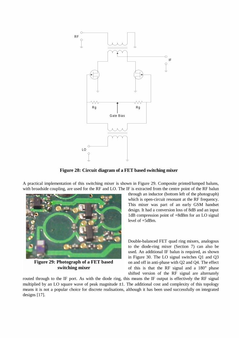
Figure 28: Circuit diagram of a FET based switching mixer
A practical implementation of this switching mixer is shown in Figure 29. Composite printed/lumped baluns, with broadside coupling, are used for the RF and LO. The IF is extracted from the centre point of the RF balun
through an inductor (bottom left of the photograph) which is open-circuit resonant at the RF frequency. This mixer was part of an early GSM handset design. It had a conversion loss of 8dB and an input 1dB compression point of +8dBm for an LO signal level of +5dBm.
Double-balanced FET quad ring mixers, analogous to the diode-ring mixer (Section 7) can also be used. An additional IF balun is required, as shown in Figure 30. The LO signal switches Q1 and Q3 on and off in anti-phase with Q2 and Q4. The effect of this is that the RF signal and a 180° phase shifted version of the RF signal are alternately
routed through to the IF port. As with the diode ring, this means the IF output is effectively the RF signal multiplied by an LO square wave of peak magnitude ±1. The additional cost and complexity of this topology means it is not a popular choice for discrete realisations, although it has been used successfully on integrated designs [17].
Figure 29: Photograph of a FET based switching mixer

IF
R F
LO
Q 1 Q 2
Q 3Q 4
Figure 30: FET quad ring mixer
7. BJT Mixers Discrete bipolar mixers tend to find applications in low cost, low power receivers such as discrete implementations of pager front ends. Designs can be compact, inexpensive and have conversion gain, however they tend to have poor linearity. Figure 31 shows two typical implementations of low cost, discrete bipolar mixers.
IF O u tput
R F sho rt-c ircu it
LO Inpu t
R F Inpu t
IF O u tput
R F sho rt-c ircu it
LO Inpu t
R F Inpu t
Figure 31: Low cost discrete bipolar mixer topologies
There is a wide range of commercially available Si bipolar integrated RF receivers and transceivers. The mixers they contain differ significantly from the discrete implementations described above. The transistors fabricated close to each other on an IC behave very similarly (they are well matched) and the die area they occupy is smaller than that occupied by passive components [18]. This leads to different circuit topologies being exploited with the almost universal choice for mixer realisation being the double-balanced “Gilbert Cell” [19] shown in Figure 32. A long-tail differential pair amplifies the RF input to the mixer. This determines the gain of the mixer and limits its linearity. The differential outputs of this amplifier are switched, by the LO signal, alternately to each of the differential IF outputs. Once again it is essentially a multiplication of the RF by ±1 at the LO frequency. This circuit relies on the different transistors being well matched and a discrete realisation is not practical.

RF input
LO input
IF output
Bias
Figure 32: Double-balanced ("Gilbert Cell") mixer
8. Image Reject Mixers Image reject mixers comprise two balanced mixers, of any topology, driven in quadrature by the RF signal. The LO drive to each mixer is in-phase and the IF output is combined in quadrature. Figure 33 shows a block diagram of an image reject mixer, the arrows representing the relative phases of the respective signals. M1 and M2 are the conversion gain/loss of the two mixers as a factor.
In-phas esplitter
R F
L O–3dB, 90° Hybrid –3dB, 90° Hybrid
2
RF
2
LO
2
LO2
RF
2
)(1 LORFM −⋅
2
)(2 LORFM −⋅
2
)(2 RFLOM −⋅
2
)(1 RFLOM −⋅
2
)(1 RFLOM −⋅
2
)(2 RFLOM −⋅
2
)(1 RFLOM −⋅
2
)(2 RFLOM −⋅2
)(2 LORFM −⋅
2
)(1 LORFM −⋅
IF o u tp u t is L O -R F (w a n te d )
2
)(1 LORFM −⋅
2
)(2 LORFM −⋅
IF o u tp u t is R F -R L O (im a g e )
Figure 33: Block diagram of an image reject mixer
To achieve perfect image cancellation, the mixers must be identical and the amplitude balance and phase shift of all quadrature and in-phase splitters perfect. An integrated solution will yield higher image rejection than a discrete and image reject mixer ICs are commercially available. With care, a discrete implementation should be able to achieve over 20dB of image rejection. The rejection of a discrete implementation can be improved if tuning of the circuit is carried out but this is not normally a viable option for high volume commercial products.

9. Summary This paper has attempted to explain the operation of RF mixers and to provide guidelines for their design. Diode, FET and BJT implementations have been considered and a number of practical examples presented.
10. References
[1] Hunter, M.T.J. “The Basics of System Design”, Proceedings of the IEE Tutorial Colloquium on “How to Design RF Circuits”, Wednesday 5th April 1999, Savoy Place, London
[2] Maas, S.A. “Microwave Mixers”, Artech House, ISBN 0-89006-605-1 [3] Walker, J.L.B. “Filters”, Proceedings of the IEE Tutorial Colloquium on “How to Design RF Circuits”,
Wednesday 5th April 1999, Savoy Place, London [4] Walker, J.L.B. ”Improvements to the Design of the 180° Rat Race Coupler and its Application to the
design of Balanced Mixers with High LO to RF Isolation”, IEEE MMT-S Digest, 1997, Vol. II, pp 747-750
[5] Maas, S.A. “Two-Tone Intermodulation in Diode Mixers”, IEEE MTT-Transactions, Vol. MTT-35, No.
3, March 1987, pp 307-314 [6] Nishizuka, N et al, “Analysis of Frequency Characteristics of Small-Sized Wide-Band Compound
Transformers”, IEEE Transactions on Magnetics, Vol. 34, No. 4, July 1998 [7] Sturdivant, R, “Balun Designs for Wireless, …Mixers, Amplifiers and Antennas”, Applied Microwave,
Summer 1993, pp 34-44 [8] Cho, C and Gupta, K.C., “A New Design Procedure for Single-Layer and Two-Layer Three-Line
Baluns”, IEEE Transactions on Microwave Theory and Techniques, Vol. 46, No. 12, December 1998, pp 2514-2519
[9] Marchand, N. “Transmission-Line Conversion”, Electronics December 1944, pp 142-145
[10] Schellenberg, J. and Hien, D, “Low-Loss Monolithic Baluns for K/Ka-Band Applications”, IEEE, MTT-
S Digest, 1999 [11] Tutt, M.N., et al, “A Low Loss, 5.5GHz – 20GHz Monolithic Balun”, IEEE MMT-S Digest, June 1997,
pp 933 - 936
[12] Ojha, S.P., Branner, G.R. and Kumar, B.P., “A Miniaturized Lumped-Distributed Balun for Modern Wireless Communication System”, IEEE MTT-S digest, 1997, pp 1347-1350
[13] Devlin, L.M. “Digitally Controlled, 6 Bit, MMIC Phase Shifter for SAR Applications”, Proceedings of
the 22nd European Microwave Conference, 1992 pp 225-230 [14] Miron, D.B., “The LC Immittance Inverter”, RF Design, January 2000, pp 20-26 [15] Tsironis, C et al, “Dual-Gate MESFET Mixers”, IEEE MTT Transactions, Vol. MTT-32, No. 3, March
1984, pp248-255 [16] Devlin, Liam, “The Design of Integrated Switches and Phase Shifters”, Proceedings of the IEE Tutorial
Colloquium on “Design of RFICs and MMICs”, Wednesday 24th November 1999, pp 2/1-14

[17] Devlin, L.M. Buck, B.J., Dearn, A.W., Clifton, J.C., Frier A.A.G., Geen, M.W., “A High Volume, Low Cost, Plastic Packaged, 2.4GHz Transceiver MMIC”, Proceedings of the third annual Wireless Symposium, Santa Clara, CA, 1995, pp 121-125
[18] Devlin, L.M., “RF ICs for Commercial Wireless Applications”, IEE tutorial colloquium on the Design of
RFICs and MMICs, 26th Nov. 1997, pp 2/1-2/11 [19] Gilbert, Barrie, “A Precise Four-Quadrant Multiplier with Subnanosecond Response”, IEEE Journal of
Solid-State Circuits, Dec. 1968, pp365-373

RF Electronics Chapter 5: Mixers Page 1
2002-2009, C. J. Kikkert, through AWR Corp.
Mixers
Introduction Figure 1 shows the typical block diagram of a Transmitter and a Receiver. It can be seen that in both cases frequency translation is achieved by the use of a Mixer. The mixers can be either passive mixers using diodes or they can be active mixers using transistors or FETs. In many receivers and transmitters, a succession of mixing and filtering stages are used, to ensure that the filtering requirements can be satisfied.
A mixer is used as an up-converter when the output frequency is higher than the input frequency. This is typical in a transmitter. A mixer is used as a down-converter when the output frequency is lower than the input frequency. This is typical for a receiver.
RF in Filter andRF Amplifier Mixer Filter and
IF AmplifierTransformer Demodulator or ADC
Mixer Filter andRF Amplifier
LocalOscillator
LocalOscillator
Filter andIF AmplifierMatching Modulator
or DACRF out
Transmitter
Receiver
Audio orData In
Audio orData Out
Figure 1. Typical transmitter and receiver block diagram.
Figure 2. Frequencies of a mixer.
Figure 2 shows the frequencies that need to be considered when using a mixer. For a down-converter the Radio Frequency (RF) signal is mixed with a Local Oscillator (LO)

RF Electronics Chapter 5: Mixers Page 2
2002-2009, C. J. Kikkert, through AWR Corp.
signal to produce sum and difference frequencies. The sum frequency is outside the operating frequency range of the system and the difference frequency is the required Intermediate Frequency (IF) signal, which is filtered and amplified using an IF filter and its associated amplifiers.
The RF filter should be sufficiently narrow so that the image frequency is not passed through the RF filter, since the difference frequency of the image frequency and the local oscillator is at exactly the same frequency as the required IF signal.
An ideal multiplier is a perfect mixer since when the LO signal is multiplied by an RF signal then sum and difference frequencies are generated, the difference frequency being the required IF signal and the sum signal being an unwanted high frequency component, which is normally filtered out. For an up-converter, the LO signal is multiplied by an IF signal and a double sideband suppressed carrier RF signal results. The aim in mixer design is thus to make the mixer behave as close to an ideal multiplier as possible.
There are two types of mixers: 1) Passive mixers, using diodes, where the LO power provides the power for the mixer. 2) Active mixers, where transistors or FETs supplied with DC power provide the mixing action.
Definition of Terms
Conversion Loss For a down-converter, the conversion loss is the ratio of the wanted IF output signal to the RF input signal. Most mixers are used in receivers, for which this definition is applicable. For up-conversion, the conversion loss is the ratio of one of the wanted RF output signal spectral components to the IF input signal. For an ideal mixer, half the input power is frequency shifted to the difference frequency and half the power is shifted to the sum frequency. The conversion loss is the ratio of either the sum or the difference component to the input signal. An ideal passive mixer will thus have a conversion loss of 3 dB. Practical balanced or double balanced mixers typically have a conversion loss of less than 6 dB. The conversion loss does depend on the amount of LO signal power applied to the LO port as can be seen in figures 11, 20 and 28. The mixer is normally operated at a LO power close to that giving the lowest conversion loss. Active mixers can have a conversion gain.
The conversion loss must be taken into account in noise figure calculations of a receiver. A mixer with a 6 dB conversion loss typically has a 6.5 dB noise figure. For high quality receivers, an amplifier with a gain much greater than the conversion loss is normally used before the mixer, to ensure that the mixer does not dominate the noise performance of the receiver.
Isolation In practice it is desirable to have isolation between the LO, RF and IF ports of the mixer. Typical double balanced mixers have more than 30 dB isolation between all ports. Single diode mixers have virtually no isolation between ports. Since single diode mixers are used in TV receivers, the LO signal is coupled to the antenna, which radiates the LO signal. In countries where TV licences are required, the detector vans look for the LO radiation and match the radiation coming from a house with any licence fee
RF Electronics Chapter 5: Mixers Page 3
2002-2009, C. J. Kikkert, through AWR Corp.
payment. One can also do a good survey to find out what TV channel people are watching by simply driving around a street with a spectrum analyser and noting the LO frequencies. For a balanced mixer, the isolation is directly related to the match between the diodes used. As a result many manufacturers sell matched sets of diodes, specially for use in mixers. In many cases two or 4 diodes come as one package.
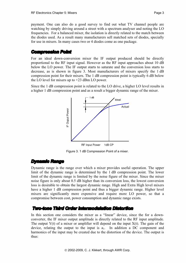
Compression Point For an ideal down-conversion mixer the IF output produced should be directly proportional to the RF input signal. However as the RF input approaches about 10 dB below the LO power. The IF output starts to saturate and the conversion loss starts to decrease, as is shown in figure 3. Most manufacturers of mixers specify the 1 dB compression point for their mixers. The 1 dB compression point is typically 6 dB below the LO level for mixers up to +23 dBm LO power.
Since the 1 dB compression point is related to the LO drive, a higher LO level results in a higher 1 dB compression point and as a result a bigger dynamic range of the mixer.
Figure 3. 1 dB Compression Point of a mixer.
Dynamic Range Dynamic range is the range over which a mixer provides useful operation. The upper limit of the dynamic range is determined by the 1 dB compression point. The lower limit of the dynamic range is limited by the noise figure of the mixer. Since the mixer noise figure is only about 0.5 dB higher than its conversion loss, the lowest conversion loss is desirable to obtain the largest dynamic range. High and Extra High level mixers have a higher 1 dB compression point and thus a bigger dynamic range. Higher level mixers are significantly more expensive and require more LO power, so that a compromise between cost, power consumption and dynamic range exists.
Two-tone Third Order Intermodulation Distortion In this section one considers the mixer as a linear device, since the for a down-converter, the IF mixer output amplitude is directly related to the RF input amplitude. The output Y(t) of a mixer or amplifier will depend on the input X(t). The gain of the device, relating the output to the input is a1. In addition a DC component and harmonics of the input may be created due to the distortion of the device. The output is thus:

RF Electronics Chapter 5: Mixers Page 4
2002-2009, C. J. Kikkert, through AWR Corp.
....)()()()()()( 55
44
33
2210 tXatXatXatXatXaatY Eqn. 1
For the devices we are considering, the terms above the 5th harmonic are so small they can be ignored.
When two signals X1 and X2 are used as input. The output will then be:
....)()()()(
)()()()()()()(5
2154
214
3213
22122110
tXtXatXtXa
tXtXatXtXatXtXaatY Eqn. 2
When X1(t) is a sinewave of frequency F1 and X2(t) is a sinewave of frequency F2 , (F2 > F1) the frequency components at the fundamental and different intermodulation frequencies can be collected as follows:
The fundamental frequency component, i.e. at F1 due to X1(t) and at F2 due to X2(t) is:
531531 425
49)
835
8310
85()
213
43( aaaaaaYF Eqn. 3
The Third Order Intermodulation (3IM) frequencies are 3IM(upper) due to F1 2F2 and 3IM(lower) due to 2F1 F2 , and are given by:
53533 825
43)
8310
215(
21
43 aaaaY IM Eqn. 4
The Fifth Order Intermodulation (5 IM) frequencies are 5IM(upper) due to 2F1 3F2
and 5IM(lower) due to 3F1 2F2 , and are given by:
555 85
8110
21 aaY IM Eqn. 5
The frequencies of these spectral components are shown in figure 4.
Figure 4. IM distortion of an amplifier or mixer.
The second order intermodulation (2IM) and the fourth order intermodulation (4IM) distortion produced by the amplifier or mixer does not create any components near the desired frequency components an as a result the 2IM and 4IM performance is less important for an amplifier. The second order intermodulation produces the required mixing action in a mixer and is thus of utmost importance.

RF Electronics Chapter 5: Mixers Page 5
2002-2009, C. J. Kikkert, through AWR Corp.
The third order IM (3IM) and fifth order IM performance is very important in linear amplifiers since when two tones are used as an input to the amplifier, the 3IM and 5IM distortion results in additional frequency components, which again can not be filtered out, as can be seen in figure 4. The 5IM components are often too small to be observed in a spectrum like figure 4. For mobile phone base-stations, these IM signals are likely to create interference in adjacent mobile phone channels, as a result the IM performance of amplifiers and mixers are a critical part of their specification.
Third Order Intercept Point In practice a1 >> a3 >> a5, so that the fundamental frequency components are proportional to a1, the 3IM components are proportional to a3 and the 5IM components are proportional to a5. If the input signals are increased by 1 dB, then the 3IM components will increase by 3 dB since they are caused by 3
213 )()( tXtXa in equation 2 and the 5IM components will increase by 5 dB since they are caused by
5215 )()( tXtXa in equation 2.
A popular method of determining the linearity of a mixer is the "third-order intercept" approach. The Third-Order Intercept Point is a theoretical point on the RF input versus IF output curve where the desired input signal and third-order products become equal in amplitude as RF input is raised.
Figure 5. Third order intercept point.
As the RF signal increases by 1 dB, the 3IM distortion component increases 3 dB. The Third Order Intercept Point is determined by increasing the RF level and noting both the desired and the 3IM levels. The third order intercept point is the point where the extension of the plotted desired output and 3IM output level versus RF input meet, as shown in figure 5. It is not possible to drive the mixer to those RF levels. As a rule of thumb the third order intercept point is about 8 to 10 dB above the LO level for a typical diode based double balanced mixer and up to 15 dB above the LO level for passive FET mixers. Passive FET mixers however have a much narrower bandwidth.
The third order intercept point is useful in determining the RF level required for a specified 3IM distortion performance. If for example, the 3IM signal is to be 40 dB below the required signal, then the RF level must be 20 dB below the Third Order Intercept Point, since then the desired signal will be 20 dB below the intercept point and the 3IM signals will be 3*20 = 60 dB below the intercept point.

RF Electronics Chapter 5: Mixers Page 6
2002-2009, C. J. Kikkert, through AWR Corp.
LO Level Mixer manufacturers make mixers to operate at different LO power levels. For standard level mixers, the LO power required is +7 dBm. Other mixer power levels are +10, +13, +17, +23, +27 dBm. Minicircuits denote their mixer according to the LO power required, so a Level 7 mixer requires a LO power of +7 dBm. For a good Double Balanced Mixer, the third order intercept point (IP3) is 10 dB above the LO level. By having a higher power level available, the manufacturers are able to control the diode I-V characteristics more to ensure that the a2 coefficient in the binomial expansion of the diode I-V characteristic shown as Equation 1, 2, 6 and 7 is maximized in relation to the other terms, thus minimizing the unwanted components.
Example A maximum RF input signal of -10 dBm and a level of third order intermodulation products (3IM) of 60 dB below the desired signals is required for a specific application. For a typical 7 level mixer, the IP3 point is +17 dBm. The RF signal at -10 dBm is thus 27 dB below the IP3 point. This will result in the 3IM signals being (3-1)*27= 54 dB below the wanted signal.
Similarly, a level 10 mixer will result in the 3IM signals being (3-1)*30 = 60 dB below the wanted signals, a level 13 mixer will result in the 3IM signals being (3-1)*33 = 66 dB below the wanted signals. A level 17 mixer will result in the 3IM signals being (3-1)*37 = 74 dB below the wanted signals. A level 23 mixer will result in the 3IM signals being (3-1)*43 = 86 dB below the wanted signals and a level 27 mixer will result in the 3IM signals being (3-1)*47 = 94 dB below the wanted signals. The higher the LO level, the higher the cost of the mixer. A level 10 mixer with thus be the lowest cost device, which will satisfy the specifications.
Single Diode Mixer Single diode mixers use a single diode to produce the required frequency components.
Single diode mixers are often used in cost critical applications, such as Radio or TV receivers, where the low cost is more important than good performance. With the advent of low cost active mixer ICs, single diode mixers are progressively being used less. Single diode mixers are very suitable for microwave applications like speed guns and shopping centre door openers, where the transmitted signal is used as the LO for the received signal, and the receiver diode is simply mounted in the antenna horn. The resulting IF signal is the difference frequency, which is due to the speed of the car being detected or the speed of the person moving towards the door.
A single diode mixer requires a diplexer to separate the high frequency RF and LO signal from the low frequency IF signal. Since the single diode mixer is normally a lower cost consumer type application, the diplexer is normally kept simple with either a first or second order high pass and low pass filters.
Figure 6 shows a simple diplexer consisting of second order high pass and low pass filters. The crossover frequency is chosen to be 20 MHz, allowing baseband signals up to 15 MHz to be used. To obtain the best impedance looking into port 1, series elements are required to connect to port 1. A Butterworth high pass and low pass filter design is a good starting point and optimisation can be used to improve the impedance matches resulting in the diplexer performance as shown in figure 7.

RF Electronics Chapter 5: Mixers Page 7
2002-2009, C. J. Kikkert, through AWR Corp.
Figure 6. Diplexer circuit.
Figure 7. Frequency response of diplexer after optimisation.
Figure 8. Circuit diagram of a single diode mixer as a down-converter.
CAPID=C1C=110.5 pF
INDID=L1L=558.9 nH
INDID=L3L=580.2 nH
CAPID=C3C=113.2 pF
PORTP=1Z=50 Ohm
PORTP=2Z=50 Ohm
PORTP=3Z=50 Ohm
SDIODEID=SchotkyEG=1.11
oo
o
n1:1
n2:1
1
2
3
4
5
XFMRTAPID=XF2N1=1N2=1
CAPID=C5C=110.5 pF
CAPID=C6C=113.2 pF
INDID=L5L=580.2 nH
INDID=L6L=558.9 nH
PORTFP=1Z=50 OhmFreq=100 MHzPwr=-5 dBm
PORT_PS1P=2Z=50 OhmPStart=0 dBmPStop=10 dBmPStep=2 dB
PORTP=3Z=50 Ohm
LO Port
RF Port
IF Port

RF Electronics Chapter 5: Mixers Page 8
2002-2009, C. J. Kikkert, through AWR Corp.
Figure 8 shows the circuit diagram of a single diode mixer. The transformer is normally not included in the circuit, since in this case it is simply a non-inverting transformer. It is included here to illustrate the differences between the single diode mixer of figure 8 and the balanced mixer of figure 19.
The mixing behaviour of a single diode mixer can be demonstrated by considering the current flowing through the diode of figure 8. The current can be expressed as:
55
44
33
2210 aaaaaa VaVaVaVaVaaI Eqn. 6
If two voltages Va and Vb are now applied to the diode, due to the LO and the RF signals, then the current will be
5
54
4
33
2210
)()()()()(
baba
bababaa
VVaVVaVVaVVaVVaaI
Eqn. 7
The term )2()( 222
22 bbaaba VVVVaVVa contains the required baVVa22 , which
results in the sum and difference frequencies. All the other terms cause unwanted frequency components. It is thus desirable to use diodes with an I-V characteristic where a2 is large in comparison with the other terms in the binomial expansion of the I-V characteristic. Some of the additional frequency components due to the a3 , a4 and higher order diode nonlinearities, can fall close to the desired frequency thus causing an interference.
Computer simulation of Mixers The advanced RF Computer simulation programs like MWO and ADS allow mixers to be simulated accurately. A mixer requires two inputs, both at different frequencies and the output is normally at a frequency that is different from both the inputs to the mixer. The simulation is thus very different from that of a linear device, like a transformer, hybrid or filter.
The frequencies used for the simulation are set by the Project Options menu. For the single diode mixer of figure 8, these frequencies are used by the PORT_PS1 port element, which is applied to the LO port (Port 2). The PORT_PS1 element allows the signal power to be varied as specified by the parameters for the PORT_PS1 element.
Figure 9. Typical Measurements for a mixer.

RF Electronics Chapter 5: Mixers Page 9
2002-2009, C. J. Kikkert, through AWR Corp.
A PORTF element produces a single tone signal with frequency and power level set by the parameters for that element. For a down-conversion mixer, the PORTF element is applied to the RF port. The RF simulation will then use these frequency and power levels to determine the time waveforms at the IF port, using a Spice modelling of the diode and the circuit. Figure 9 shows the typical measurements that can be made on a mixer. The first one is the conversion loss.
Figure 10. Parameters for conversion loss measurements.
The conversion loss of the mixer can be determined as the LO power level is varied, by setting the relevant parameters of the PORT_PS1 element to provide a power level sweep at the LO port. The sum or difference frequency that is analysed for determining the conversion loss is set by the parameters for the Large Signal S parameter (LSSnm) measurement shown in figure 10. The conversion loss is determined as the ratio of the power levels at the specified frequencies of port 1 as input and port 3 as output.
For a realistic determination of performance of the mixer, a LO frequency of 105 MHz and an RF frequency of 100 MHz with a level of -5 dBm is chosen. The project frequency is set as a single frequency at 105 MHz. If a range of frequencies are specified, then one or all of these can be used for the conversion loss. It is thus possible to determine the conversion loss for a range of LO frequencies as well. For a LO input at 105 MHz and an RF input at 100 MHz, the desired IF output is at 5 MHz. The appropriate harmonic index combinations are selected such that the input is at 100 MHz and the output is at 5 MHz, as indicated in figure 10. MWO automatically calculates the relevant frequency as the harmonic indices are changed.
Figure 11 shows the resulting conversion loss as a function of LO power level for the single diode mixer of figure 8. Note that the conversion loss decreases with an increasing LO drive level. A higher LO power level increases the power consumption of the mixer, requires a higher power LO source and dissipates more heat. By comparing figures 11 and 20, it can be seen that the conversion loss of the single diode mixer is very poor.
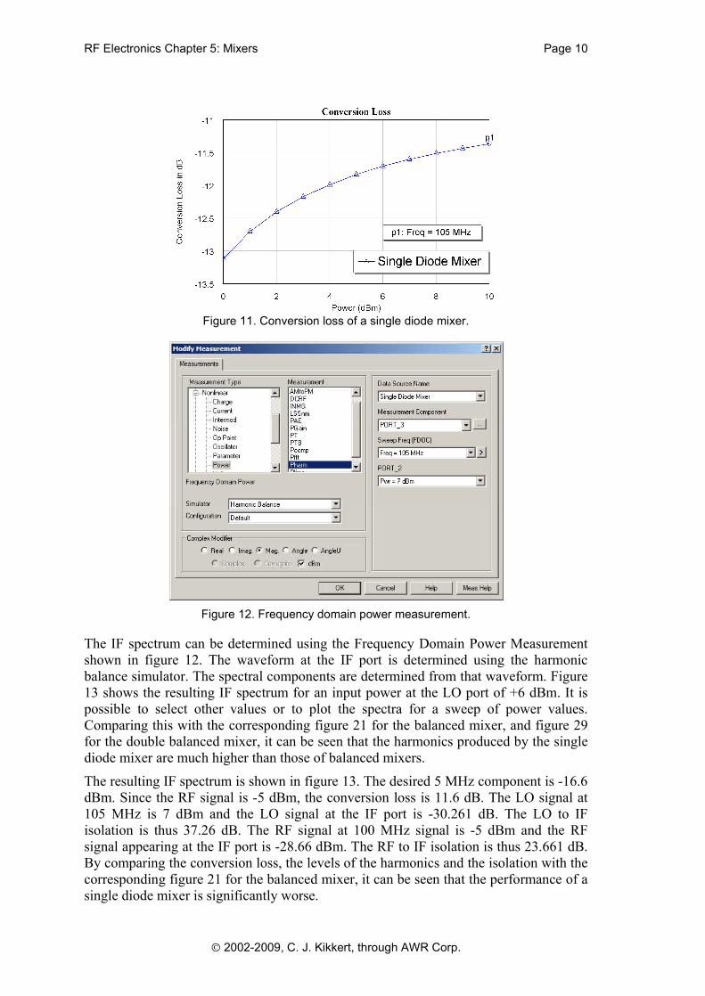
RF Electronics Chapter 5: Mixers Page 10
2002-2009, C. J. Kikkert, through AWR Corp.
Figure 11. Conversion loss of a single diode mixer.
Figure 12. Frequency domain power measurement.
The IF spectrum can be determined using the Frequency Domain Power Measurement shown in figure 12. The waveform at the IF port is determined using the harmonic balance simulator. The spectral components are determined from that waveform. Figure 13 shows the resulting IF spectrum for an input power at the LO port of +6 dBm. It is possible to select other values or to plot the spectra for a sweep of power values. Comparing this with the corresponding figure 21 for the balanced mixer, and figure 29 for the double balanced mixer, it can be seen that the harmonics produced by the single diode mixer are much higher than those of balanced mixers.
The resulting IF spectrum is shown in figure 13. The desired 5 MHz component is -16.6 dBm. Since the RF signal is -5 dBm, the conversion loss is 11.6 dB. The LO signal at 105 MHz is 7 dBm and the LO signal at the IF port is -30.261 dB. The LO to IF isolation is thus 37.26 dB. The RF signal at 100 MHz signal is -5 dBm and the RF signal appearing at the IF port is -28.66 dBm. The RF to IF isolation is thus 23.661 dB. By comparing the conversion loss, the levels of the harmonics and the isolation with the corresponding figure 21 for the balanced mixer, it can be seen that the performance of a single diode mixer is significantly worse.

RF Electronics Chapter 5: Mixers Page 11
2002-2009, C. J. Kikkert, through AWR Corp.
Figure 13. IF spectrum of a single diode mixer as a down-converter.
If a two-tone RF input signal is used, the single diode mixer has a high level of IM components. As a result, the single diode mixer requires more stringent RF filtering to avoid those IM signals being generated by the mixer and appearing in the IF output. The single diode mixer also requires more stringent IF filtering to remove those unwanted IF components from the IF signal, to prevent the unwanted signals from effecting the demodulated output from the receiver. Most AM radios use single diode mixers and this is one reason why their performance is poor compared to FM radios.
The voltage and current time waveforms can also be determined, using the Vtime and Itime measurements. The measurements can be done at a single LO power level or at a range of levels as is done by selecting plot all traces instead of the 0 dBm level in the Port_2 entry of the Itime measurement window shown in figure 14. Alternately, as has been done in this project, a limited power sweep can be obtained by performing multiple single level measurements as shown in figure 9.
Figure 14. Itime measurement setting.

RF Electronics Chapter 5: Mixers Page 12
2002-2009, C. J. Kikkert, through AWR Corp.
Figure 15. IF currents for a single diode mixer as a down-converter.
Figure 15 shows the resulting IF currents of a single diode mixer, notice with the 2nd order filters used in the diplexer, there is still significant RF current components present in the IF signal. A higher order filter will improve the isolation, but will not improve the performance sufficiently to justify the additional cost. For the frequencies used, the output spectra and conversion loss will be the same if higher order diplexer filters are used. As can be seen from figure 15, the single diode mixer has a significant DC current component, which changes with LO drive level.
To operate the mixer as an up-converter, the PORTF element is applied to the IF port and the signal generated by that port is set to 5 MHz and a power of -5 dBm. The mixer output is then at the RF port. The resulting circuit diagram for the single diode mixer as an up-converter is shown in figure 16. The same measurements can be performed as for the down-converter.
Figure 16. Circuit diagram of a single diode mixer as an up-converter.
The RF output spectrum is shown in figure 17. From this spectrum it can be seen that the conversion loss, being the amplitude of the 100 MHz RF component due to the 5 MHz IF signal is the same as for the down-converter. The components around 100 MHz show a large 105 MHz LO component in the RF output, indicating only a 8.6 dB LO-RF isolation. The LO spectral component at the RF port is larger than any of the wanted
SDIODEID=SchotkyEG=1.11
oo
o
n1:1
n2:1
1
2
3
4
5
XFMRTAPID=XF2N1=1N2=1
CAPID=C6C=113.2 pF
INDID=L5L=580.2 nH
INDID=L6L=558.9 nH CAP
ID=C1C=110.5 pF
PORTFP=1Z=50 OhmFreq=5 MHzPwr=-5 dBm
PORT_PS1P=2Z=50 OhmPStart=0 dBmPStop=10 dBmPStep=2 dB
PORTP=3Z=50 Ohm
LO Port
RF Port
IF Port
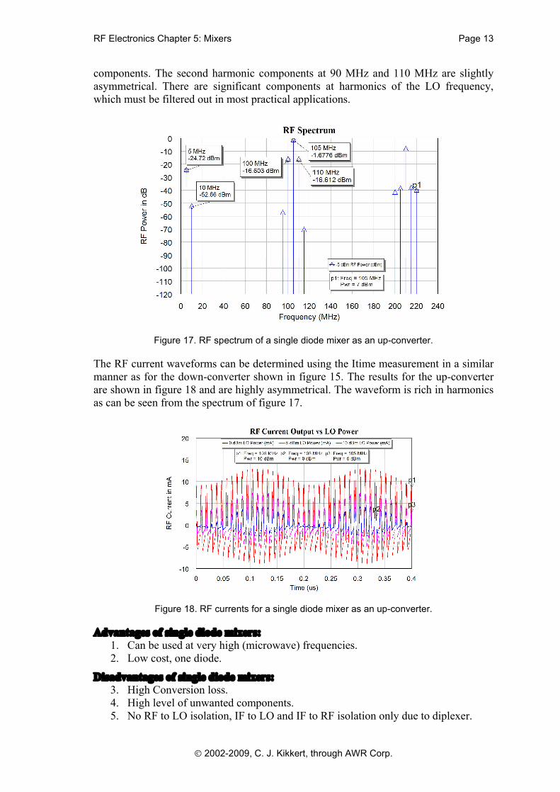
RF Electronics Chapter 5: Mixers Page 13
2002-2009, C. J. Kikkert, through AWR Corp.
components. The second harmonic components at 90 MHz and 110 MHz are slightly asymmetrical. There are significant components at harmonics of the LO frequency, which must be filtered out in most practical applications.
Figure 17. RF spectrum of a single diode mixer as an up-converter.
The RF current waveforms can be determined using the Itime measurement in a similar manner as for the down-converter shown in figure 15. The results for the up-converter are shown in figure 18 and are highly asymmetrical. The waveform is rich in harmonics as can be seen from the spectrum of figure 17.
Figure 18. RF currents for a single diode mixer as an up-converter.
Advantages of single diode mixers: 1. Can be used at very high (microwave) frequencies. 2. Low cost, one diode.
Disadvantages of single diode mixers: 3. High Conversion loss. 4. High level of unwanted components. 5. No RF to LO isolation, IF to LO and IF to RF isolation only due to diplexer.

RF Electronics Chapter 5: Mixers Page 14
2002-2009, C. J. Kikkert, through AWR Corp.
Balanced Mixer Adding a second diode to the circuit shown in figure 19 results in a balanced mixer. The first diode has Va+Vb across it and the second diode has Va-Vb where voltage Va is the LO and Vb is the RF voltage. The currents through the diodes are thus:
5
54
4
33
22101
)()()()()(
baba
bababaD
VVaVVaVVaVVaVVaaI
Eqn. 8
5
54
4
33
22102
)()()()()(
baba
bababaD
VVaVVaVVaVVaVVaaI
Eqn. 9
The difference between the diode currents flows into the IF port and RF port, so that the current flowing through the IF and RF port is:
5
532
54
533
4
3232121
22010)(8
2642
bbabababa
bbababDDRFIF
VaVVaVVaVVVVa
VVVaVVaVaIII Eqn. 10
For a single diode mixer the current through the IF and RF port is the same as is shown in equation 8. Comparing equation 10 with equation 8, it can be seen that most of the unwanted components cancel. The only components that are in the IF band are:
)(84 3342 bababaIF VVVVaVVaI Eqn. 11
Which is close to ideal multiplication as the a4 term is normally very small.
Since the LO voltage, Va >> the RF voltage, Vb , the VaVb and the Va3Vb terms
dominate. The Vb and the Va2Vb terms do not produce any frequency components in the
region of interest. For an ideal mixer one wants the a, c, d and e components to be as small as possible, the manufacturers of mixers ensure their diodes satisfy this as much as possible. The balanced mixer will thus have a much better performance than the single diode mixer.
Figure 19. Circuit diagram of a balanced mixer.
The circuit diagram of the balanced mixer is shown in figure 19. The only difference between that and the circuit for the single diode mixer of figure 8 is the use of the second diode, but having the second diode results in a significant performance improvement.
SDIODEID=SchotkyEG=1.11
oo
o
n1:1
n2:1
1
2
3
4
5
XFMRTAPID=XF2N1=1N2=1 CAP
ID=C5C=110.5 pF
CAPID=C6C=113.2 pF
INDID=L5L=580.2 nH
INDID=L6L=558.9 nH
SDIODEID=Schotky1EG=1.11
PORTFP=1Z=50 OhmFreq=100 MHzPwr=-5 dBm
PORT_PS1P=2Z=50 OhmPStart=0 dBmPStop=10 dBmPStep=1 dB
PORTP=3Z=50 Ohm
LO PortRF Port
IF Port

RF Electronics Chapter 5: Mixers Page 15
2002-2009, C. J. Kikkert, through AWR Corp.
Figure 20. Conversion loss of a balanced diode mixer.
The conversion loss of the mixer is shown in figure 20. The conversion loss is far less than that of a single diode mixer. For LO levels of around 7 dBm, any variation in LO power does not cause any change in conversion loss, so that the mixer is then very insensitive to AM noise of the LO. This is an important advantage of the balanced mixer over the single diode mixer.
Figure 21. IF spectrum of a balanced diode mixer as a down-converter.
Figure 21 shows the IF spectrum of the balanced mixer. As expected from the equation 10, many of the unwanted spectral components have significantly reduced amplitudes compared with the single diode mixer. The second harmonic of the desired IF signal, at 10 MHz and caused by the mixing process, is more than 40 dB below the desired 5 MHz signal. The LO signal appearing in the IF spectrum is -87.9 dBm, since the LO signal is 7 dBm, the LO to IF isolation is 94.9 dB.
The RF signal appearing at the IF port is -31.939 dBm. Since the RF signal is -5 dBm, The RF to IF is isolation is 26.9 dB. This can only be improved by using a higher order diplexer as part of the mixer, or by using another mixer configuration like the double balanced mixer.
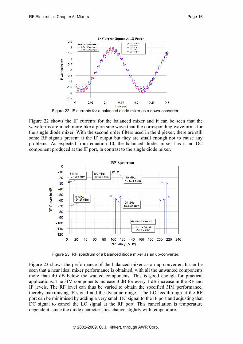
RF Electronics Chapter 5: Mixers Page 16
2002-2009, C. J. Kikkert, through AWR Corp.
Figure 22. IF currents for a balanced diode mixer as a down-converter.
Figure 22 shows the IF currents for the balanced mixer and it can be seen that the waveforms are much more like a pure sine wave than the corresponding waveforms for the single diode mixer. With the second order filters used in the diplexer, there are still some RF signals present at the IF output but they are small enough not to cause any problems. As expected from equation 10, the balanced diodes mixer has is no DC component produced at the IF port, in contrast to the single diode mixer.
Figure 23. RF spectrum of a balanced diode mixer as an up-converter.
Figure 23 shows the performance of the balanced mixer as an up-converter. It can be seen that a near ideal mixer performance is obtained, with all the unwanted components more than 40 dB below the wanted components. This is good enough for practical applications. The 3IM components increase 3 dB for every 1 dB increase in the RF and IF levels. The RF level can thus be varied to obtain the specified 3IM performance, thereby maximising IF signal and the dynamic range. The LO feedthrough at the RF port can be minimised by adding a very small DC signal to the IF port and adjusting that DC signal to cancel the LO signal at the RF port. This cancellation is temperature dependent, since the diode characteristics change slightly with temperature.
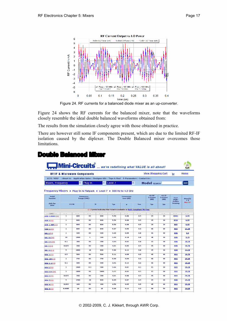
RF Electronics Chapter 5: Mixers Page 17
2002-2009, C. J. Kikkert, through AWR Corp.
Figure 24. RF currents for a balanced diode mixer as an up-converter.
Figure 24 shows the RF currents for the balanced mixer, note that the waveforms closely resemble the ideal double balanced waveforms obtained from:
The results from the simulation closely agree with those obtained in practice.
There are however still some IF components present, which are due to the limited RF-IF isolation caused by the diplexer. The Double Balanced mixer overcomes those limitations.
Double Balanced Mixer
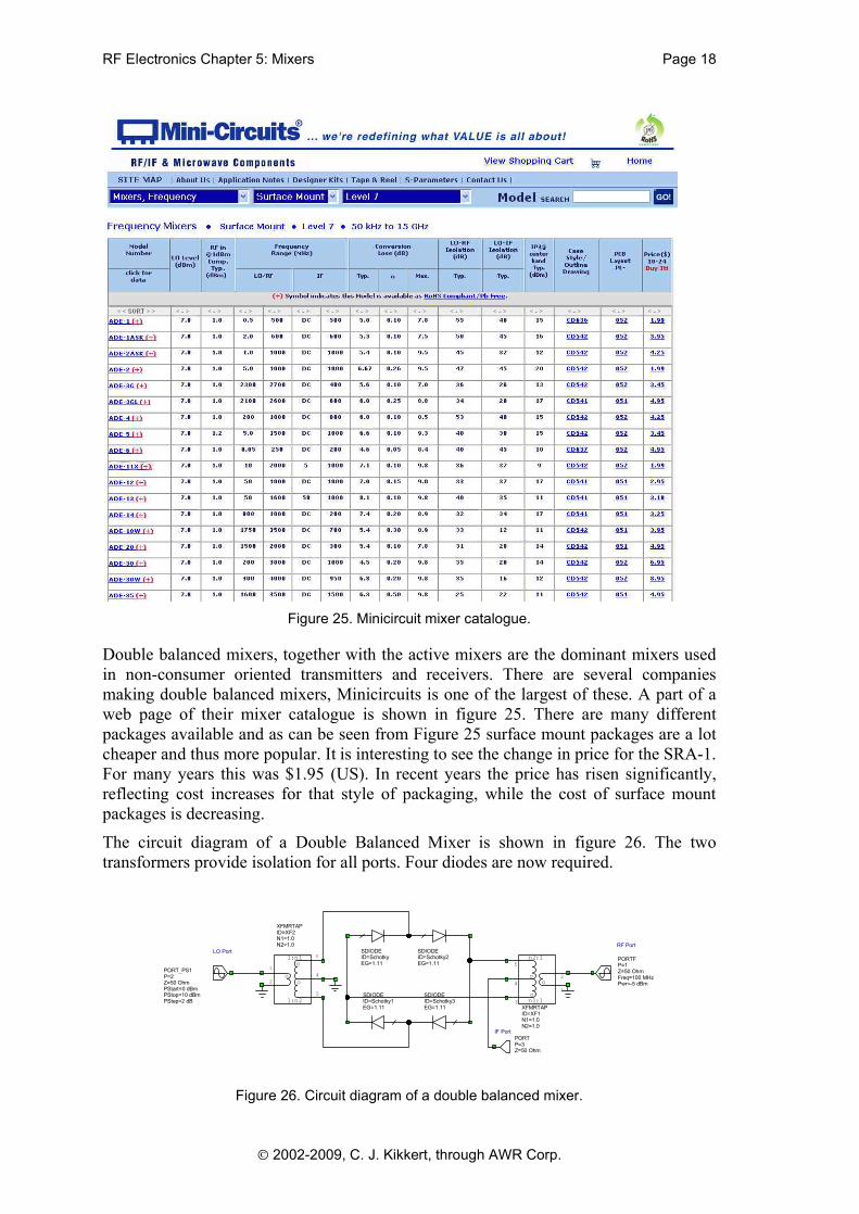
RF Electronics Chapter 5: Mixers Page 18
2002-2009, C. J. Kikkert, through AWR Corp.
Figure 25. Minicircuit mixer catalogue.
Double balanced mixers, together with the active mixers are the dominant mixers used in non-consumer oriented transmitters and receivers. There are several companies making double balanced mixers, Minicircuits is one of the largest of these. A part of a web page of their mixer catalogue is shown in figure 25. There are many different packages available and as can be seen from Figure 25 surface mount packages are a lot cheaper and thus more popular. It is interesting to see the change in price for the SRA-1. For many years this was $1.95 (US). In recent years the price has risen significantly, reflecting cost increases for that style of packaging, while the cost of surface mount packages is decreasing.
The circuit diagram of a Double Balanced Mixer is shown in figure 26. The two transformers provide isolation for all ports. Four diodes are now required.
Figure 26. Circuit diagram of a double balanced mixer.
SDIODEID=SchotkyEG=1.11
oo
o
n1:1
n2:1
1
2
3
4
5
XFMRTAPID=XF2N1=1.0N2=1.0
SDIODEID=Schotky1EG=1.11
SDIODEID=Schotky2EG=1.11
SDIODEID=Schotky3EG=1.11
oo
o
n1:1
n2:1
1
2
3
4
5
XFMRTAPID=XF1N1=1.0N2=1.0
PORTFP=1Z=50 OhmFreq=100 MHzPwr=-5 dBm
PORT_PS1P=2Z=50 OhmPStart=0 dBmPStop=10 dBmPStep=2 dB
PORTP=3Z=50 Ohm
LO PortRF Port
IF Port

RF Electronics Chapter 5: Mixers Page 19
2002-2009, C. J. Kikkert, through AWR Corp.
Figure 27a Mixer with +ve voltage applied at the IF port.
For the analysis of the mixer consists of considering what happens if a +ve input signal is applied to the IF port. Under those conditions the diodes shown in figure 27a conduct and the others are an open circuit. As a result a positive signal applied to the LO port, then a positive signal is obtained at the RF port.
Figure 27 b. Mixer with ve voltage applied at the IF port.
If a -ve input signal is applied to the IF port, the diodes shown in figure 27b conduct and the others are an open circuit. As a result if a positive signal is applied to the LO port, then a positive signal is obtained at the RF port. If a zero voltage signal is applied at the IF port all the diodes are equal resistances and the LO signal is cancelled at the RF port. In practice having a smaller IF voltage results in a smaller RF voltage. The RF signal is thus the LO signal multiplied by the IF signal, resulting in a proper mixing action.
Figure 28. Conversion loss of a double balanced diode mixer.
SDIODEID=SchotkyEG=1.11
oo
o
n1:1
n2:1
1
2
3
4
5
XFMRTAPID=XF2N1=1.0N2=1.0
SDIODEID=Schotky3EG=1.11
oo
o
n1:1
n2:1
1
2
3
4
5
XFMRTAPID=XF1N1=1.0N2=1.0
PORTFP=1Z=50 OhmFreq=100 MHzPwr=-5 dBm
PORT_PS1P=2Z=50 OhmPStart=0 dBmPStop=10 dBmPStep=2 dB
PORTP=3Z=50 Ohm
LO PortRF Port
IF Port
oo
o
n1:1
n2:1
1
2
3
4
5
XFMRTAPID=XF2N1=1.0N2=1.0
oo
o
n1:1
n2:1
1
2
3
4
5
XFMRTAPID=XF1N1=1.0N2=1.0
SDIODEID=Schotky1EG=1.11
SDIODEID=Schotky2EG=1.11
PORTFP=1Z=50 OhmFreq=100 MHzPwr=-5 dBm
PORT_PS1P=2Z=50 OhmPStart=0 dBmPStop=10 dBmPStep=2 dB
PORTP=3Z=50 Ohm
LO PortRF Port
IF Port

RF Electronics Chapter 5: Mixers Page 20
2002-2009, C. J. Kikkert, through AWR Corp.
Figure 28 shows that the conversion loss of a Double Balanced Mixer is approximately 0.5 dB less than that of a balanced mixer and more than 6 dB less than that of a single diode mixer. Comparing the IF spectrum of a down-converting Double Balanced Mixer as shown in figure 29 this with the corresponding figures 13 and 21 for single and balanced diode mixers, it can be seen that there are no spectral components in the 80 to 120 MHz frequency range. The difference signal at 5 MHz and the sum signal at 205 MHz are the same amplitude. The signal at 215 MHz is due to the third harmonic of the input signal mixing with the local oscillator. In a receiver, these harmonic signals must be evaluated, to ensure that they do not cause signals in the IF frequency band.
Figure 29. IF spectrum of a double balanced diode mixer as a down-converter.
Figure 30. IF currents for a balanced diode mixer as a down-converter.
Figure 30 shows the IF currents. There is a significant high frequency content. Figure 31 shows the same IF currents with the IF signal passed through a 25 MHz low pass filter to remove the high frequency components. The waveform looks like an ideal Sine wave and there is little change in the output as the LO power is changes between 0 dBm and 10 dBm. The LO AM noise will thus have little effect on the IF output.

RF Electronics Chapter 5: Mixers Page 21
2002-2009, C. J. Kikkert, through AWR Corp.
Figure 31. IF currents of figure 29 with frequency components >25 MHz removed.
Figure 32. RF spectrum of a double balanced diode mixer as an up-converter.
Figure 33. RF currents for a double Balanced Diode Mixer as an up-converter.

RF Electronics Chapter 5: Mixers Page 22
2002-2009, C. J. Kikkert, through AWR Corp.
Figure 32 shows the RF spectrum of a double balanced mixer as an up-converter. The desired spectrum around the 105 MHz LO is ideal, with no unwanted spectral components. Figure 33 shows the corresponding RF currents. The spectrum and the waveform is very similar to that for an ideal multiplier. Double balanced mixers can be used as analogue multipliers in applications like a phase detector or a true RMS power meter.
Figure 34 shows the construction of a simple home made double balanced mixer, the transformers are held in-place with Silastic (Silicone Sealant). The diodes are conventional Shottky-Barrier diodes that have been matched for their V-I characteristic in order to obtain the best LO RF isolation.
Figure 34. Construction of a Double Balanced Mixer for use in Practical Sessions.
Figure 35. Measured performance of the mixer of figure 34.

RF Electronics Chapter 5: Mixers Page 23
2002-2009, C. J. Kikkert, through AWR Corp.
The measured performance of the mixer is shown in Figure 35. The transformers for this mixer were designed for operation at 1 MHz, as a result an IF frequency of 250 kHz and an LO of 10 MHz was used for the spectrum in figure 35. For the measurement of figure 35, the LO signal was at a frequency of 10 MHz and a level of +7 dBm. The IF signal was at a frequency of 300 Hz and a level of -10 dBm. The measured conversion loss is 6 dB and the LO RF isolation is -60 dB. This mixer performs well for RF and LO signals in the range of 30 kHz to 30 MHz and IF signals up to 30 MHz.
Comparing the spectrum around the LO in figure 35 with the corresponding spectrum around the LO in figure 32, shows that in practice there will be some LO RF carrier feed-through due to a slight mismatch of the diodes. Figure 35 shows that the 5IM distortion components, 1.250 MHz from the LO frequency at the centre of the plot, are bigger than the 3IM components , 750 kHz from the LO frequency.
Microwave Mixers At microwave frequencies (>1 GHz) transformers become difficult to make. In addition the capacitance associated with the diodes used in the mixer cause the diodes to become less efficient as a mixer. As a result, mixers at microwave frequencies have higher conversion losses than mixers used at lower frequencies. Conversion losses of 6 to 10 dB are typical. Transformer based mixers are available for frequencies up to 12 GHz.
At microwave frequencies, transmission lines are often used to produce the two outputs with a 180 phase shift, to provide a replacement for the transformer in the balanced mixer shown the figure 19. The circuit for the corresponding microwave mixer is shown in figure 36. In this design, the mixer is used for a down-converter for a weather satellite receiver and uses a 1565 MHz Local Oscillator to shift a 1700 MHz RF signal to a 135 MHz IF frequency.
Figure 36. Circuit diagram of a Microwave Balanced mixer.
The conversion loss for this mixer is shown in figure 37, and is 0.3 dB less than the conversion loss for corresponding transformer based mixer, shown in figure 20. Figure 38 shows the spectrum for the mixer as a down converter. The mixer performs well and the spectrum is similar to that of the transformer based mixer in figure 21.
Changing the transformer to a transmission line will thus not change the performance of the mixer very much apart from a reduction of the bandwidth, since the transmission line only produces a 180 phase shift at a single frequency. However in many
SDIODEID=Schotky1
SDIODEID=Schotky2 CAP
ID=C1C=4.5 pF
TLINID=TL1Z0=50 OhmEL=180 DegF0=1565 MHz
TLINID=TL2Z0=70.7 OhmEL=90 DegF0=1565 MHz IND
ID=L2L=22.5 nH
CAPID=C2C=4.5 pF
TLSCID=TL3Z0=50 OhmEL=90 DegF0=1565 MHz
TLSCID=TL4Z0=50 OhmEL=90 DegF0=1565 MHz
INDID=L3L=22.4 nH
PORT_PS1P=2Z=50 OhmPStart=0 dBmPStop=10 dBmPStep=1 dB
PORTFP=1Z=50 OhmFreq=1700 MHzPwr=-5 dBm
PORTP=3Z=50 Ohm
RF Port
LO Port
IF Port
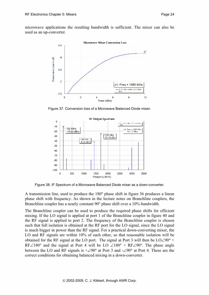
RF Electronics Chapter 5: Mixers Page 24
2002-2009, C. J. Kikkert, through AWR Corp.
microwave applications the resulting bandwidth is sufficient. The mixer can also be used as an up-converter.
Figure 37. Conversion loss of a Microwave Balanced Diode mixer.
Figure 38. IF Spectrum of a Microwave Balanced Diode mixer as a down-converter.
A transmission line, used to produce the 180 phase shift in figure 36 produces a linear phase shift with frequency. As shown in the lecture notes on Branchline couplers, the Branchline coupler has a nearly constant 90 phase shift over a 10% bandwidth. The Branchline coupler can be used to produce the required phase shifts for efficient mixing. If the LO signal is applied at port 1 of the Branchline coupler in figure 40 and the RF signal is applied to port 2. The frequency of the Branchline coupler is chosen such that full isolation is obtained at the RF port for the LO signal, since the LO signal is much bigger in power than the RF signal. For a practical down-converting mixer, the LO and RF signals are within 10% of each other, so that reasonable isolation will be obtained for the RF signal at the LO port. The signal at Port 3 will then be LO 90 + RF 180 and the signal at Port 4 will be LO 180 + RF 90 . The phase angle between the LO and RF signals is + 90 at Port 3 and - 90 at Port 4. These are the correct conditions for obtaining balanced mixing in a down-converter.

RF Electronics Chapter 5: Mixers Page 25
2002-2009, C. J. Kikkert, through AWR Corp.
Microwave mixer using a Branchline Coupler
Figure 39. Circuit diagram of a balanced mixer with a Branchline coupler.
Figure 40. Circuit diagram the Branchline coupler used as a subcircuit in Figure 39.
Correct biasing for the diodes must be provided, such that all the RF and LO energy is dissipated in the diodes and all the resulting low frequency energy is passed to the IF port and is not reflected back into the RF or LO ports.
The transmission lines consisting of TL12 and TL8 and consisting of TL11 and TL14 are also one quarter wavelength long at the RF and LO frequencies and thus form a short circuit at those frequencies and an open circuit at the IF frequency. All the RF and LO energy coming from the Branchline coupler is thus dissipated in the diodes.
The Short circuited transmission lines consisting of TL9 and TL4 and consisting of TL10 and TL5 are one quarter wavelength long at the LO and RF frequencies, so that they are an open circuit at the LO and RF frequencies and a short circuit at the IF frequency. All the frequency components at the IF signal band are thus passed unhindered to the IF port 3 of the mixer. To make the removal of the LO and RF signals at the IF port as effective as possible, the size of capacitor C1 is chosen to act as a short circuit to the RF and LO signals but have little effect at the IF frequency.
SDIODEID=Schotky1
SDIODEID=Schotky2
12
3
MTEEID=TL1W1=3 mmW2=W50 mmW3=1 mm
1 2
3MTEEID=TL2W1=W50 mmW2=3 mmW3=1 mm
MLSCID=TL4W=1 mmL=LIFS mm
MLSCID=TL5W=1 mmL=LIFS mm
MLINID=TL6W=W50 mmL=LI1 mm
12
3
MTEEID=TL7W1=W50 mmW2=3 mmW3=3 mm
MLEFID=TL8W=3 mmL=LRFS mm
1 2
3
MTEEID=TL13W1=3 mmW2=W50 mmW3=3 mm
1
2
3
MTEEID=TL15W1=W50 mmW2=W50 mmW3=W50 mm
MLINID=TL18W=W50 mmL=17 mm
MCURVEID=TL11W=3 mmANG=90 DegR=5 mm
MCURVEID=TL12W=3 mmANG=90 DegR=5 mm
MCURVEID=TL19ANG=90 DegR=3 mm
MCURVEID=TL20ANG=90 DegR=3 mm
MCURVEID=TL10W=1 mmANG=90 DegR=5 mm
MCURVEID=TL9W=1 mmANG=90 DegR=5 mm
MSUBEr=3.38H=0.8128 mmT=0.035 mmRho=0.7Tand=0.0027ErNom=3.38Name=RO/RO1
CAPID=C1C=4 pF
MLINID=TL3W=W50 mmL=LI1 mm
MLINID=TL16W=W50 mmL=LI2 mm
MLINID=TL17W=W50 mmL=LI2 mm
MLINID=TL21W=W50 mmL=10 mm
1 2
3
MTEEID=TL22W1=W50 mmW2=W50 mmW3=3 mm
MLEFID=TL14W=3 mmL=LRFS mm
1
2
3
4
SUBCKTID=S1NET="Branchline"
PORTFP=1Z=50 OhmFreq=1700 MHzPwr=-11.5 dBm
PORT_PS1P=2Z=50 OhmPStart=0 dBmPStop=10 dBmPStep=1 dB
PORTP=3Z=50 Ohm
LIFS=21.68LRFS=19.39
LI1=4LI2=6.557
MLINID=TL1W=W35 mmL=L2 mm
MLINID=TL4W=W35 mmL=L2 mm
1 2
3
MTEE$ID=TL5
12
3
MTEE$ID=TL6
1 2
3
MTEE$ID=TL7
12
3
MTEE$ID=TL8
MSUBEr=3.38H=0.8128 mmT=0.035 mmRho=0.7Tand=0.0027ErNom=3.38Name=RO1
MLINID=TL9W=W50 mmL=5 mm
MLINID=TL10W=W50 mmL=5 mm
MLINID=TL11W=W50 mmL=5 mm
MLINID=TL12W=W50 mmL=5 mm
MCURVEID=TL22ANG=90 DegR=RB mm
MCURVEID=TL2ANG=90 DegR=RB mm
MCURVEID=TL3ANG=90 DegR=RB mm
MCURVEID=TL13ANG=90 DegR=RB mm
MCURVEID=TL14ANG=90 DegR=RB mm
MCURVEID=TL15ANG=90 DegR=RB mm
MCURVEID=TL17ANG=90 DegR=RB mm
MCURVEID=TL18ANG=90 DegR=RB mm
PORTP=1Z=50 Ohm
PORTP=3Z=50 Ohm
PORTP=4Z=50 Ohm
PORTP=2Z=50 Ohm
RB=4.46 W50=1.851L3=28.7L2=L3-W50/2
L1=27.7W35=3.13
W50C=1.83
LO
RF
LO(Ang90) + RF(Ang180)
LO(Ang180) + RF(Ang90)
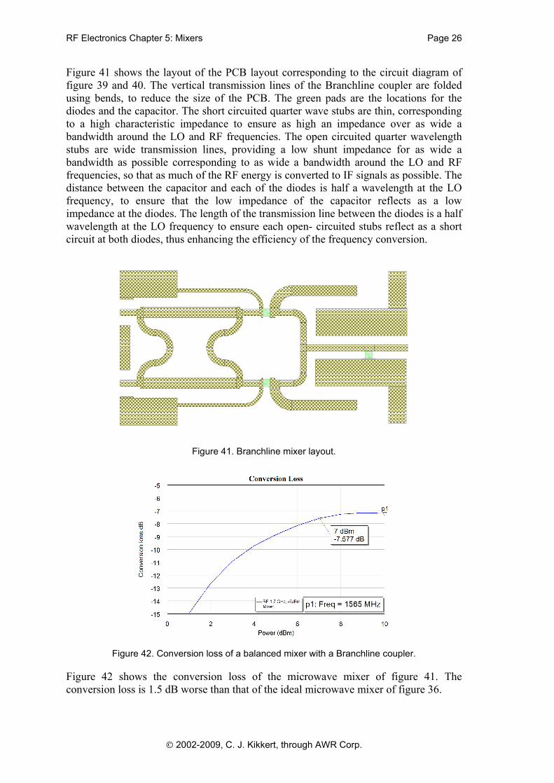
RF Electronics Chapter 5: Mixers Page 26
2002-2009, C. J. Kikkert, through AWR Corp.
Figure 41 shows the layout of the PCB layout corresponding to the circuit diagram of figure 39 and 40. The vertical transmission lines of the Branchline coupler are folded using bends, to reduce the size of the PCB. The green pads are the locations for the diodes and the capacitor. The short circuited quarter wave stubs are thin, corresponding to a high characteristic impedance to ensure as high an impedance over as wide a bandwidth around the LO and RF frequencies. The open circuited quarter wavelength stubs are wide transmission lines, providing a low shunt impedance for as wide a bandwidth as possible corresponding to as wide a bandwidth around the LO and RF frequencies, so that as much of the RF energy is converted to IF signals as possible. The distance between the capacitor and each of the diodes is half a wavelength at the LO frequency, to ensure that the low impedance of the capacitor reflects as a low impedance at the diodes. The length of the transmission line between the diodes is a half wavelength at the LO frequency to ensure each open- circuited stubs reflect as a short circuit at both diodes, thus enhancing the efficiency of the frequency conversion.
Figure 41. Branchline mixer layout.
Figure 42. Conversion loss of a balanced mixer with a Branchline coupler.
Figure 42 shows the conversion loss of the microwave mixer of figure 41. The conversion loss is 1.5 dB worse than that of the ideal microwave mixer of figure 36.
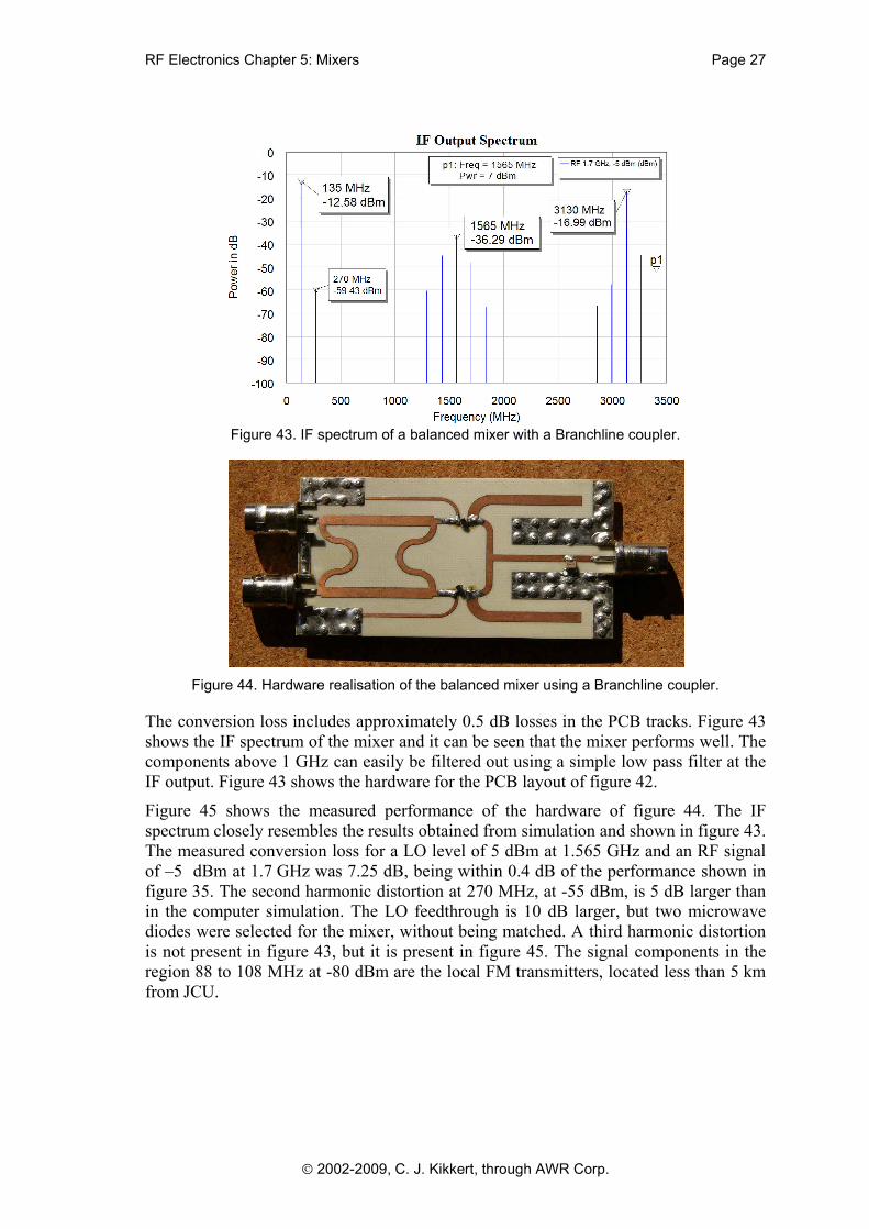
RF Electronics Chapter 5: Mixers Page 27
2002-2009, C. J. Kikkert, through AWR Corp.
Figure 43. IF spectrum of a balanced mixer with a Branchline coupler.
Figure 44. Hardware realisation of the balanced mixer using a Branchline coupler.
The conversion loss includes approximately 0.5 dB losses in the PCB tracks. Figure 43 shows the IF spectrum of the mixer and it can be seen that the mixer performs well. The components above 1 GHz can easily be filtered out using a simple low pass filter at the IF output. Figure 43 shows the hardware for the PCB layout of figure 42.
Figure 45 shows the measured performance of the hardware of figure 44. The IF spectrum closely resembles the results obtained from simulation and shown in figure 43. The measured conversion loss for a LO level of 5 dBm at 1.565 GHz and an RF signal of 5 dBm at 1.7 GHz was 7.25 dB, being within 0.4 dB of the performance shown in figure 35. The second harmonic distortion at 270 MHz, at -55 dBm, is 5 dB larger than in the computer simulation. The LO feedthrough is 10 dB larger, but two microwave diodes were selected for the mixer, without being matched. A third harmonic distortion is not present in figure 43, but it is present in figure 45. The signal components in the region 88 to 108 MHz at -80 dBm are the local FM transmitters, located less than 5 km from JCU.

RF Electronics Chapter 5: Mixers Page 28
2002-2009, C. J. Kikkert, through AWR Corp.
Figure. 45, Measured spectrum of Branchline coupler mixer of figure 44.
Active Single transistor mixer
Figure 46. Active single diode mixer (AWR example, Low_Power_Mixer).
Figure 46 shows the Low_Power_Mixer active single diode mixer from the Microwave office mixer examples. An active single transistor mixer has a similar spectral performance to a passive single diode mixer, but has a conversion gain. The mixer of figure 46 has a conversion gain of more than 10 dB. Active single transistor mixers are used in many consumer devices like radio and TV.
CAPID=CrfC=1.8 pF
0 V 0 mA
I_METERID=ICC10.755 V
0.516 mA
DCVSID=VCC1V=1 V
1 V0.521 mA
RESID=R1R=470 Ohm
0.521 mA
RESID=R2R=8200 Ohm
0.00511 mA
INDID=LifL=270 nH
0.516 mA
INDID=LrfL=6.6 nH
0.00511 mA
CAPID=CpIFC=33 pF
0 V
0.755 V0 mA CAP
ID=CsIFC=13.3 pF
0 V0 mA
CAPID=CloC=0.5 pF
0.713 V0 mA
0 V
RESID=RLR=RL Ohm
0 mA
CAPID=DC_block1C=2e5 pF
0.713 V0 mA CAP
ID=DC_block2C=2e5 pF
0.755 V0 mA
Xo Xn. . .
SWPVARID=PloSwpVarName="Plo"Values=stepped(-70,-35,5)UnitType=PowerLog
Xo Xn. . .
SWPVARID=PrfSwpVarName="Prf"Values=stepped(-80,-50,5)UnitType=PowerLog
Xo Xn. . .
SWPVARID=RLSwpVarName="RL"Values= 1500,4700 UnitType=Resistance
C
B
E
1
2
3
SUBCKTID=S1NET="MMBR941"
0.00511 mA
0.516 mA
PORTP=3Z=50 Ohm
0 V0 mA
PORT1P=1Z=50 OhmPwr=Plo dBW
0 V0 mA
PORTFP=2Z=50 OhmFreq=900 MHzPwr=Prf dBW
0 V0 mA
Plo=-40
Prf=-80
RL=1500

RF Electronics Chapter 5: Mixers Page 29
2002-2009, C. J. Kikkert, through AWR Corp.
Gilbert Cell Active Mixer: It is possible to use two transistors in a push-push amplifier configuration and thus produce an active balanced mixer. However, the Gilbert Cell or long tail multiplier is much more commonly used as an active mixer, as it provides close to ideal multiplier performance. The Gilbert cell mixer is used in many ICs. There is a Gilbert-Cell mixer in the examples provided by MWO. That Gilbert cell example has been simplified to illustrate its principle of operation as shown in figure 45. Gilbert Cell mixers with very good IM performances and a frequency range from DC to 5 GHz are available.
Figure 47 shows the basic circuit diagram of a Gilbert Cell mixer. Normally all these components would be included in an IC. Figure 48 shows the corresponding conversion gain. The LO and RF frequencies are chosen to be the same as that for the microwave mixer of figure 36 and 39. The circuit consists of 3 parts, the left part consisting of transistors TR1 to TR7 is the Gilbert Cell multiplier. Transistor TR1 is a constant current source for the long tail pair amplifiers making up the Gilbert Cell. The resistor chain R1 to R4 is a biasing chain, providing the biasing voltages. Transistors TR8 to TR11 form the output buffer amplifier, with transistors TR9 and TR11 being constant current sources and TR8 and TR10 being voltage followers.
A fully differential output circuit is required to obtain the best LO isolation, without having to tune the RL13 and RL24 for best LO IF isolation. The differential IF output also minimises the IF harmonic output at 270 MHz.
Figure 47. Basic Gilbert Cell active multiplier.
The Gilbert Cell mixer is different from the diode mixers in that the best performance is obtained when the LO signal does not cause saturation in the transistors of the Gilbert Cell. Figure 48 shows that the largest signal that can be used without the mixer saturating too much is -6 dBm and that level of LO power has been used for the
RESID=RIFR=25 Ohm
RESID=RSHL23R=50 Ohm
RESID=RSHL4R=50 Ohm
DCVSID=V1V=12 V
RESID=RL13R=400 Ohm
RESID=R1R=1000 Ohm
RESID=R2R=550 Ohm
RESID=R3R=500 Ohm
RESID=R4R=450 Ohm
RESID=RQB3R=27 Ohm
RESID=RQB2R=27 Ohm
RESID=RSHR1R=50 Ohm
RESID=RSHR2R=50 Ohm
CAPID=C2_RFINC=1e4 pF
CAPID=C1_LOINC=1e4 pF
CAPID=COUTC=1e5 pF
CAPID=CRFC=1e5 pF
CAPID=CLOC=1e5 pF
C
B
E
1
2
3
GBJT3ID=TR4
C
B
E
1
2
3
GBJT3ID=TR5
C
B
E
1
2
3
GBJT3ID=TR6
C
B
E
1
2
3
GBJT3ID=TR7
C
B
E
1
2
3
GBJT3ID=TR1
C
B
E
1
2
3
GBJT3ID=TR8
C
B
E
1
2
3
GBJT3ID=TR2
RESID=RL24R=400 Ohm
C
B
E
1
2
3
GBJT3ID=TR9
CAPID=CRF1C=1e5 pF
CAPID=CRF2C=1e5 pF
CAPID=CRF3C=1e5 pF
C
B
E
1
2
3
GBJT3ID=TR3
CAPID=COUT1C=1e5 pF
C
B
E
1
2
3
GBJT3ID=TR10
C
B
E
1
2
3
GBJT3ID=TR11
RESID=RIF1R=25 Ohm
RESID=RQB1R=27 Ohm
o o1:n11
2
3
4
XFMRID=X1N=1
PORT_PS1P=1Z=50 OhmPStart=-15 dBmPStop=0 dBmPStep=3 dB
PORTFP=2Z=50 OhmFreq=1700 MHzPwr=-18 dBm
PORTP=3Z=50 Ohm
LO
RF
+IF
-IF
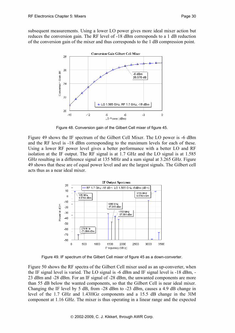
RF Electronics Chapter 5: Mixers Page 30
2002-2009, C. J. Kikkert, through AWR Corp.
subsequent measurements. Using a lower LO power gives more ideal mixer action but reduces the conversion gain. The RF level of -18 dBm corresponds to a 1 dB reduction of the conversion gain of the mixer and thus corresponds to the 1 dB compression point.
Figure 48. Conversion gain of the Gilbert Cell mixer of figure 45.
Figure 49 shows the IF spectrum of the Gilbert Cell Mixer. The LO power is -6 dBm and the RF level is -18 dBm corresponding to the maximum levels for each of these. Using a lower RF power level gives a better performance with a better LO and RF isolation at the IF output. The RF signal is at 1.7 GHz and the LO signal is at 1.585 GHz resulting in a difference signal at 135 MHz and a sum signal at 3.265 GHz. Figure 49 shows that these are of equal power level and are the largest signals. The Gilbert cell acts thus as a near ideal mixer.
Figure 49. IF spectrum of the Gilbert Cell mixer of figure 45 as a down-converter.
Figure 50 shows the RF spectra of the Gilbert Cell mixer used as an up-converter, when the IF signal level is varied. The LO signal is -6 dBm and IF signal level is -18 dBm, -23 dBm and -28 dBm. For an IF signal of -28 dBm, the unwanted components are more than 55 dB below the wanted components, so that the Gilbert Cell is near ideal mixer. Changing the IF level by 5 dB, from -28 dBm to -23 dBm, causes a 4.9 dB change in level of the 1.7 GHz and 1.43HGz components and a 15.5 dB change in the 3IM component at 1.16 GHz. The mixer is thus operating in a linear range and the expected
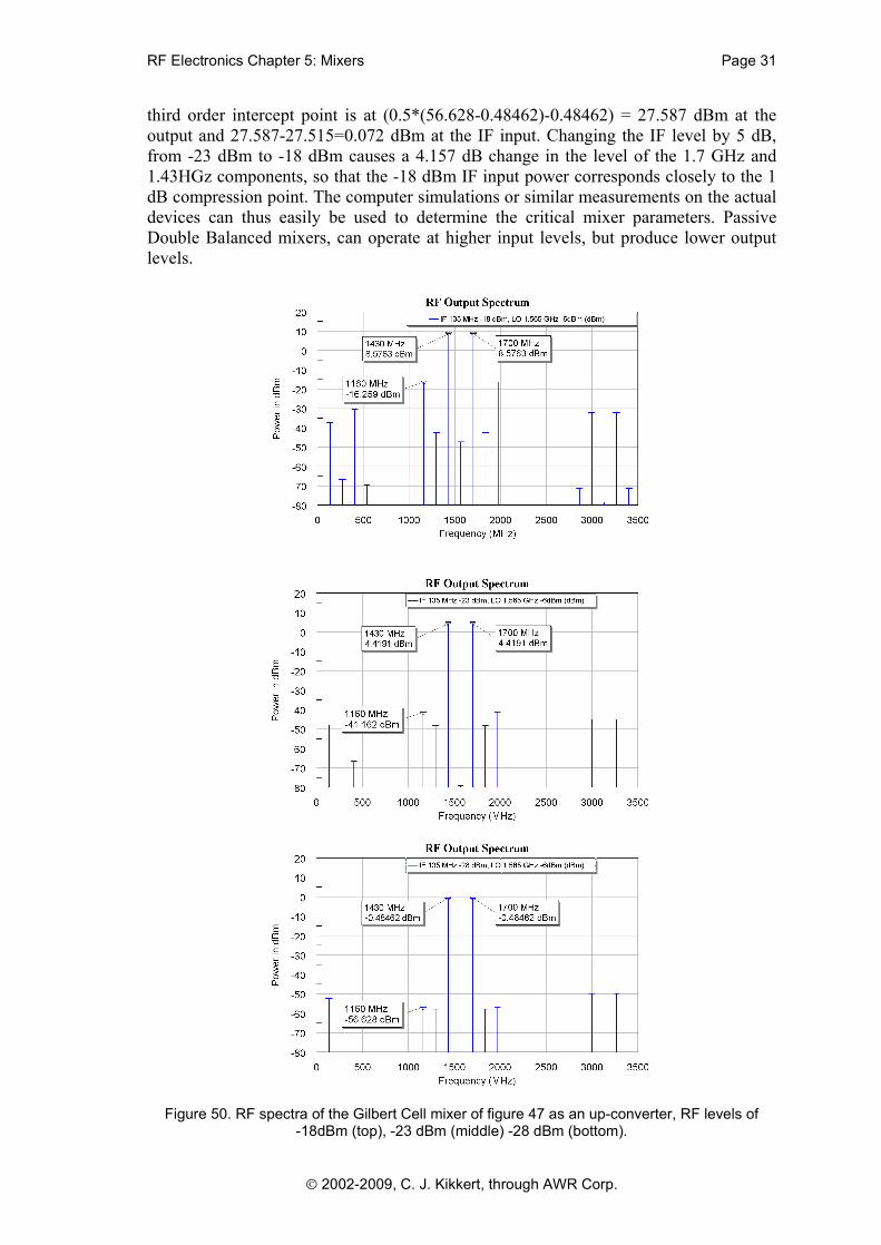
RF Electronics Chapter 5: Mixers Page 31
2002-2009, C. J. Kikkert, through AWR Corp.
third order intercept point is at (0.5*(56.628-0.48462)-0.48462) = 27.587 dBm at the output and 27.587-27.515=0.072 dBm at the IF input. Changing the IF level by 5 dB, from -23 dBm to -18 dBm causes a 4.157 dB change in the level of the 1.7 GHz and 1.43HGz components, so that the -18 dBm IF input power corresponds closely to the 1 dB compression point. The computer simulations or similar measurements on the actual devices can thus easily be used to determine the critical mixer parameters. Passive Double Balanced mixers, can operate at higher input levels, but produce lower output levels.
Figure 50. RF spectra of the Gilbert Cell mixer of figure 47 as an up-converter, RF levels of
-18dBm (top), -23 dBm (middle) -28 dBm (bottom).
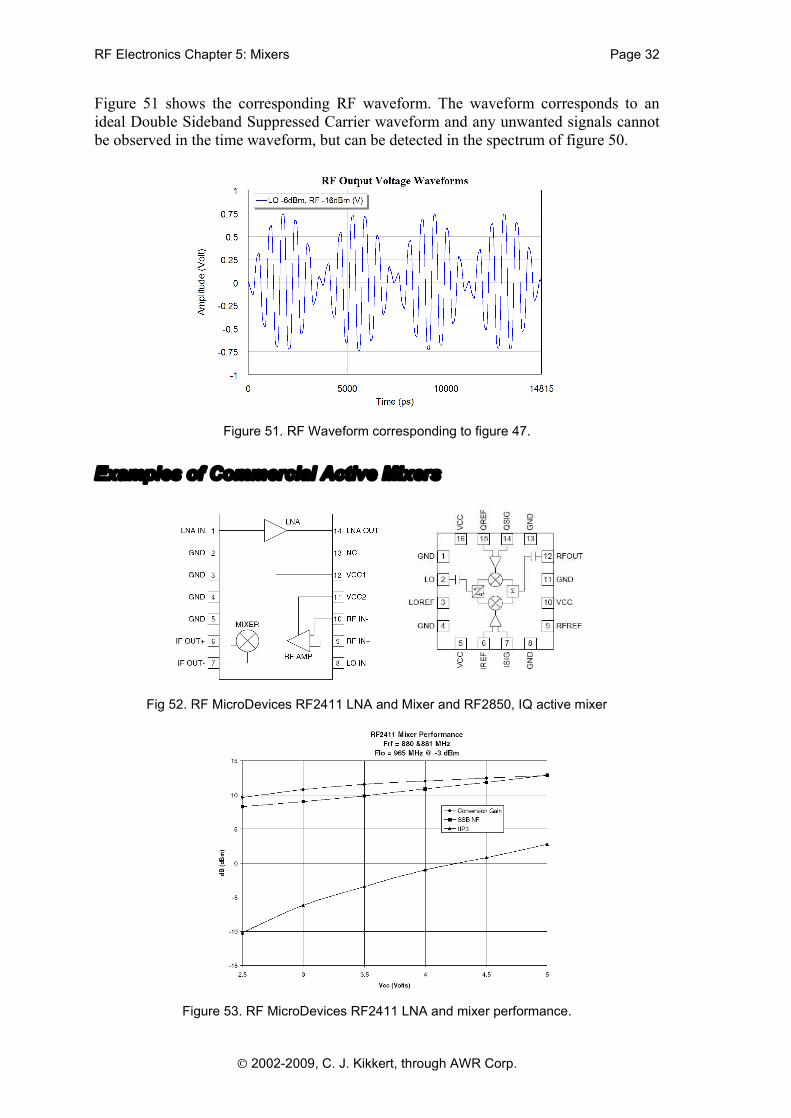
RF Electronics Chapter 5: Mixers Page 32
2002-2009, C. J. Kikkert, through AWR Corp.
Figure 51 shows the corresponding RF waveform. The waveform corresponds to an ideal Double Sideband Suppressed Carrier waveform and any unwanted signals cannot be observed in the time waveform, but can be detected in the spectrum of figure 50.
Figure 51. RF Waveform corresponding to figure 47.
Examples of Commercial Active Mixers
Fig 52. RF MicroDevices RF2411 LNA and Mixer and RF2850, IQ active mixer
Figure 53. RF MicroDevices RF2411 LNA and mixer performance.

RF Electronics Chapter 5: Mixers Page 33
2002-2009, C. J. Kikkert, through AWR Corp.
Many manufacturers produce active mixers for use in commercial equipment. In particular mixers for use in mobile and cordless phones, wireless LANs and similar consumer devices are readily available. The RF2411 Receiver front end and the RF2850 IQ active mixer, produced by RF MicroDevices are some examples of commercial active mixers. Figure 52 shows the pin connections of two commercial mixer ICs.
As shown in figure 53, the LNA used in the RF2411 IC, has a noise figure which varies from 1.7 dB at 500 MHz to 2.5 dB at 1500 MHz. The gain of the LNA is 17 dB at 1 MHz and slopes to 11 dB at 1500 MHz. The RF2411 can thus be used in many commercial applications.
Quadrature Mixers
Figure 54. Block diagram of a quadrature mixer.
In quadrature mixers a 90 degree hybrid, like a Branchline coupler is used to produce two LO signals, corresponding to Sine and Cosine of the LO frequency. The Cosine signal is then multiplied with the In-Phase (I) component of the baseband signal, and the Sine signal is multiplied with the Quadrature (Q) component of the baseband signal, as shown in figure 54. The resulting signals are then added using a combiner like a Wilkinson hybrid to produce the RF signal. When the I and Q signals are the Hilbert transform of each other, then a Single Sideband RF signal results. When the I and Q signals are an RF signal that is passed through a 90 hybrid then the image frequency components are suppressed. When the I and Q signals are individually controlled baseband signals a vector modulated RF signal results. In most cases the I and Q signals are produced using Digital Signal Processing techniques. Quadrature mixers are thus required for the vector modulation used in many modern communication systems.
The 90 Degree hybrids required for quadrature mixers can also be produced using LC networks, so that quadrature hybrids at frequencies below 500 MHz are possible. As an example, Minicircuits make quadrature mixers at a wide range of frequencies as shown in figure 55.
Local oscillators produced using phase locked loops or using Direct Digital Synthesis, can have two outputs which have an exact 90 degree phase difference over a wide range of frequencies, as is required for the quadrature mixers.

RF Electronics Chapter 5: Mixers Page 34
2002-2009, C. J. Kikkert, through AWR Corp.
Fig 55. Minicircuit IQ mixers. (From their catalogue)
Active IQ Mixers The RF2850 IQ mixer shown in figure 52, is used as an up-converter for mobile radio applications. This mixer used Gilbert cells for the mixers. Using an IQ mixer allows the required RF output signal to be produced, without the need to filter out unwanted sidebands. In addition a zero IF frequency can be used, so that the LO is at the centre of the RF band, again avoiding the need for filters. Such RF filters are large and heavy. It is desirable to have a small and light mobile phone. An I and Q signal, up to 250 MHz can be used, together with a LO signal in the range 1.7 GHz to 2.5 GHz, to produce a quadrature modulated RF signal in the range 1.7 GHz to 2.5 GHz. A typical carrier suppression of 25 dB unadjusted and 55 dB adjusted is obtained. The mixer has a typical (unadjusted) unwanted sideband suppression of 45 dB. The mixer performance satisfies all the mobile radio standards. These are low cost devices aimed for a consumer market.
For modern signal generators, IQ modulation is used to produce the complex modulated waveforms used in modern communication systems. The mixers used in such signal generators are often active (Gilbert cell) IQ mixers. Computer controlled DC bias (control and calibration) signals are used to ensure that the carrier feed-through, Quadrature phase shifts and I and Q gains are correct. The design of such ICs can cost more than one million dollars. The resulting devices have a better performance than those of figure 55 or 56, but each mixer will also be more expensive.
LTC Mixers At higher frequencies, it becomes more difficult to wind the transformers required for the mixers. Low Temperature Cofired (LTC) thick film technology allows a circuit to be made up from multiple layers of ceramic materials. By depositing conductive of magnetic inks, a set of layers can form a strip-line transmission line, a ferrite loaded hybrid or it can contain semiconductor elements like diodes. Because high dielectric constant materials are used, the resulting package can be made small. Since the process can be automated, lower production costs result. Minicircuits use this technology for

RF Electronics Chapter 5: Mixers Page 35
2002-2009, C. J. Kikkert, through AWR Corp.
producing high frequency mixers. A typical example is their IQBG-2000 I&Q modulator. The block diagram is the same as the IQ mixer in figure 54. This device is designed for the 1.8 GHz to 2 GHz mobile phone market. The Package is shown in figure 56. This LTC IQ mixer has an image rejection of better than 30 dB, which is comparable to the transformer based mixers shown in figure 53, but this isolation could not be obtained using conventional transformer based technology. More details on LTC circuits are given in the lectures on Circuit Manufacture.
Fig 56. Minicircuits LTC IQ mixer, IQBG-2000. (From www.minicircuits.com)
Other Mixers Mixer manufacturers make other types of mixers, such as triple balanced mixers, which result in a better input impedance and double balanced mixers using FETs in a passive mode (no DC supplied to the FET) in order to obtain an improved IP3 performance. The description of such devices are beyond the scope of these notes, but some further details can be found at the Minicircuits web site (www.minicircuits.com).