Embed Size (px)
Citation preview
MICROWAVE INTEGRATED PHASED-ARRAY TRANSMITTERS IN SILICON
Thesis by
Abbas Komijani
In Partial Fulfillment of the Requirements
For the Degree of
Doctor of Philosophy
CALIFORNIA INSTITUTE OF TECHNOLOGY
Pasadena, California
2006
(Defended August 22, 2006)

ii
© 2006
Abbas Komijani
All Rights Reserved

iii
Acknowledgement
I would like to express my deep and sincere gratitude to all who made this work
possible. I am especially grateful to Professor Ali Hajimiri for his constant support and
guidance throughout my Ph.D. studies. His broad vision, together with his remarkable
knowledge of our field of research, has proved to be invaluable in defining my research
direction. He has been a great instructor, supervisor, and friend.
I would like to thank my other committee members: Dr. Sander Weinreb, Professor
David Rutledge, Professor Shuki Bruck, Professor Changhuei Yang, and Dr. Larry
D'Addario for their assistance, helpful comments, and insightful suggestions.
I am also grateful to my colleagues: Arun Natarajan, Xiang Guan, Aydin Babakhani,
Hossein Hashemi, Ehsan Afshari, Behnam Analui, James Buckwalter, Ichiro Aoki, Scott
Kee, Donhee Ham, Hui Wu, Roberto Aparicio, Chris White, Yu-Jiu Wang, Hua Wang,
Edward Keehr, Florian Bohr, and Sam Mandegaran. This work would not have been
possible without their help.
I would also like to thank the Caltech staff: Michelle Chen, Naveed Near-Ansari, John
Lilley, Niklas Wadefalk, Linda Dozsa, Jim Endrizzi, and Tess Legaspi, whose support
has created a student-friendly environment.
This research has been supported by the Lee Center for Advanced Networking, the
Office of Naval Research, the National Science Foundation, and trusted foundry program
of DARPA.
I am thankful to my supportive friend, Payman Shanjani, who has always encouraged
me to excel.
I would like to thank my loving parents, who have taught me to achieve my goals, and

iv
my brothers and sisters, who have always believed in me. Their unconditional love has
been the greatest source of energy to me.
My greatest thanks are due to Shiva, my beloved wife, whose caring, understanding,
and positive attitude have always encouraged me to go forward during difficult times.
Her never-ending love and support are what made the completion of this work possible.
v
Abstract
Phased-array systems, a special case of multiple-input-multiple-output (MIMO)
systems, take advantage of spatial directivity and array gain to increase spectral
efficiency. Implementing a phased-array system at high frequency in a commercial
silicon process technology presents several challenges. This thesis focuses on the
architectural and circuit-level trade-offs involved in the design of the silicon-based fully
integrated phased-array transmitters.
As the first implementation, a four-element 24GHz 0.18µm CMOS phased-array
transmitter with integrated power amplifiers is presented. On-chip power amplifiers use
substrate-shielded slow-wave transmission lines for impedance matching and can
generate up to 14dBm of output power. The transmitter employs a two-step upconversion
architecture with 4.8GHz as the intermediate frequency (IF) and uses a single 19.2GHz
synthesizer serving as the local oscillator (LO) generator. The phased-array, employing
the LO phase shifting architecture, achieves 23dB of peak to null-ratio when all four
elements are used, demonstrates a beam steering range covering all signal incident angles,
and can support a data rate of 500Mbps with a quadrature phase-shift keying (QPSK)
baseband signal.
As the second implementation with a modified phase shifting architecture, an integrated
4-element 77GHz Silicon-Germanium (SiGe) phased-array transceiver is presented. Two-
step conversion, envisioning a dual-mode 77GHz/24GHz operation, is used at both the
receiver and the transmitter paths. A differential phase of 52GHz is generated by the on-
chip voltage-controlled oscillator (VCO) and is distributed to all radio frequency (RF)
paths. The phase shifting is performed at the LO ports of the RF mixers with continuous
analog phase shifters. The quadrature signal of the second LO, at the IF frequency of
vi
26GHz, is generated by dividing the VCO frequency by a factor of 2 using a cross-
coupled injection-locked frequency divider. The on-chip 77GHz power amplifier with an
output power of 17.5dBm and peak power added efficiency (PAE) of 14% achieves the
best performance demonstrated in silicon. A single transmitter path achieves a 40dB
conversion gain at 77GHz with 2.5GHz of bandwidth and a maximum output power of
12.5dBm.
The measured results demonstrate the feasibility of using silicon-based integrated
phased-arrays for wireless communication and vehicular radar applications.

vii
Contents
Acknowledgements iii
Abstract v
List of Figures x
List of Tables xv
Chapter 1 Introduction..................................................................................................... 1
1.1 Organization ........................................................................................................2
Chapter 2 Fundamentals of Multi-Path Transceivers................................................... 4
2.1 A Historical Note ................................................................................................5
2.2 High Frequency Circuit Design: Challenges and Opportunities .........................6
2.3 Phased-Array Principles ......................................................................................8
2.4 Phased-Arrays: A Special Case of Multiple-Input Multiple-Output (MIMO) Systems....................................................................................................................13
2.5 Phased-Array Applications ...............................................................................14
2.6 Phased-Array Architectures ..............................................................................19
2.6.1 Time Delay vs. Phase Shift................................................................... 19
2.6.2 Implementation of the Phase Shift: Choice of Architecture................. 21
2.6.3 Effects of Narrowband Approximation ................................................ 24
2.6.4 Using OFDM to Remedy the Error Caused by the Constant Phase Shift Approximation............................................................................................... 28
2.7 Wireless Communication at Millimeter-Wave Frequencies .............................30
2.8 Chapter Summary..............................................................................................33
Chapter 3 A 24GHz, +14.5dBm Fully-Integrated Power Amplifier in 0.18μm CMOS........................................................................................................................................... 35
3.1 Introduction .......................................................................................................36

viii
3.2 Power Requirements in the 24GHz Band..........................................................37
3.3 Circuit Design ...................................................................................................38
3.3.1 Substrate-Shielded Coplanar Waveguide Structure.............................. 38
3.3.2 Characterization of the Substrate-Shielded CPW Structure ................. 41
3.3.3 Single-Transistor Power Gain and Stability ......................................... 44
3.3.4 Stability of the Cascode Pair................................................................. 46
3.3.5 Amplifier Design .................................................................................. 48
3.3.6 Low-Frequency Stability of the Amplifier ........................................... 50
3.3.7 Wirebond and Pad Parasitic Effects ..................................................... 50
3.4 Experimental Results.........................................................................................51
3.5 Chapter Summary..............................................................................................57
Chapter 4 A Fully-Integrated 24GHz Phased-Array Transmitter in CMOS........... 58
4.1 Introduction .......................................................................................................58
4.2 Transmitter Architecture ...................................................................................60
4.3 Power Amplifier and on-chip Balun .................................................................65
4.4 Experimental Results.........................................................................................67
4.5 Chapter Summary..............................................................................................76
Chapter 5 A Wideband 77GHz, 17.5dBm Fully-Integrated Power Amplifier in Silicon............................................................................................................................... 77
5.1 Introduction .......................................................................................................77
5.2 The Required Amplifier Power for Automotive RADAR Application ............78
5.3 Conductor-Backed Coplanar Waveguide as the Transmission Line Structure .80
5.4 Amplifier Design...............................................................................................84
5.4.1 Circuit Schematic and Bias................................................................... 84
5.4.2 Design of the Matching Networks........................................................ 87
5.4.3 Output Stage Power Combining ........................................................... 89
5.4.4 Simulation and Layout Methodology ................................................... 91
5.5 Measurement Results ........................................................................................93
ix
5.6 Chapter Summary..............................................................................................99
Chapter 6 A 77GHz Fully-Integrated Phased-Array Transceiver........................... 101
6.1 Introduction .....................................................................................................102
6.2 Local LO-Path Phase-Shifting Architecture....................................................104
6.3 Transceiver Architecture .................................................................................107
6.4 Circuit Design .................................................................................................111
6.4.1 52GHz Phase Rotator ......................................................................... 111
6.4.2 Power Amplifier and On-Chip Image-Rejection Filter ...................... 115
6.4.3 IF and RF Stages................................................................................. 116
6.4.4 52GHz Voltage-Controlled Oscillator................................................ 118
6.5 Measurement Results ......................................................................................119
6.6 Chapter Summary............................................................................................128
Chapter 7 Conclusion ................................................................................................... 129
7.1 Recommendations for Future Work................................................................130
Bibliography 147
x
List of Figures
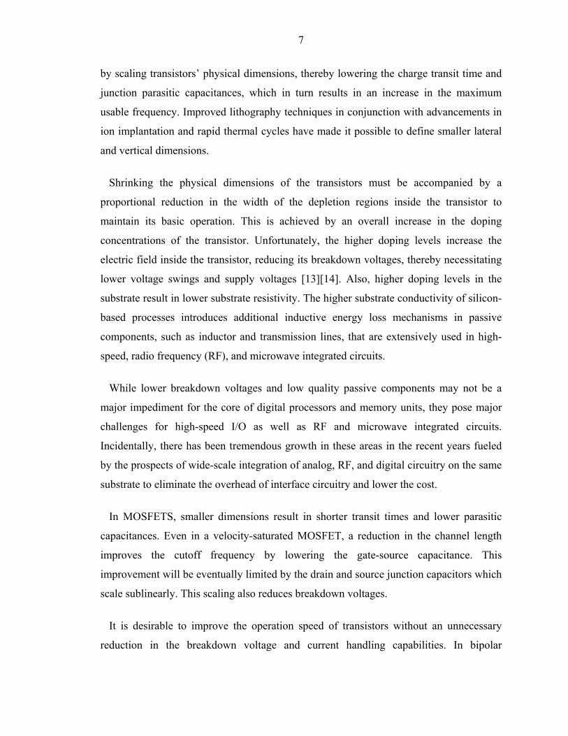
Figure 2.1 (a) Phased-array transmitter focuses the beam at a desired angle. (b) Phased-array receiver focuses on desired signal while it attenuates interferer coming from other direction. ............................................................................................................................. 9
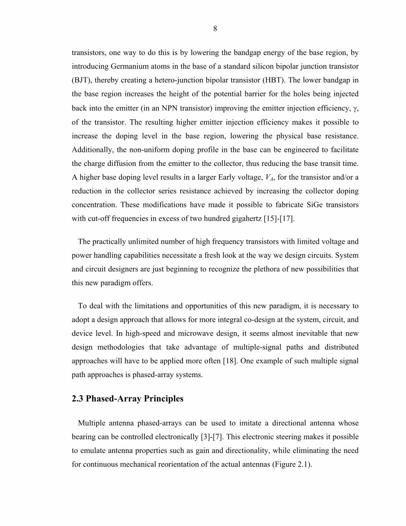
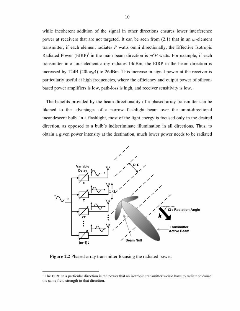
Figure 2.2 Phased-array transmitter focusing the radiated power. .................................. 10
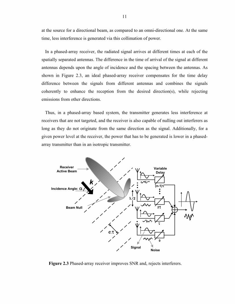
Figure 2.3 Phased-array receiver improves SNR and, rejects interferers. ....................... 11
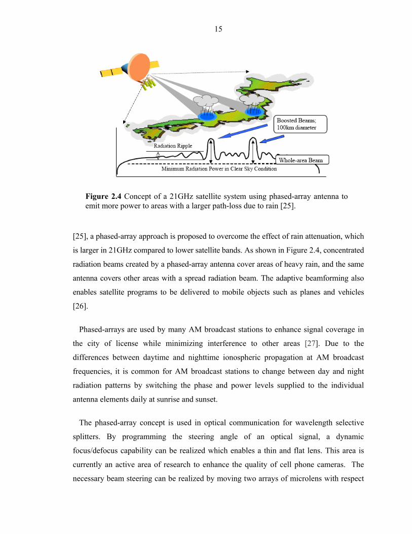
Figure 2.4 Concept of a 21GHz satellite system using phased-array antenna to emit more power to areas with a larger path-loss due to rain [25]..................................................... 15
Figure 2.5 Automotive radar sensors providing multiple driving-aid functions............. 17
Figure 2.6 Narrowband approximation of a delay with a constant phase shift................ 20
Figure 2.7 Understanding the source of dispersion in a phased-array transmitter when a time delay is approximated with a constant phase shift. (a) Time delay in RF provides wideband beam forming. (b) Equivalent system by moving the delay before the mixer. (c)(d) Elimination of time delay in baseband results in dispersion. Note that only phase shift is required now, and it can be implemented in the LO, IF, or RF paths................... 20
Figure 2.8 Different architectures for implementing phase shift. (a) RF phase shifting. (b) IF phase shifting. (c) Digital phase shifting. (d) LO-path phase shifting. ........................ 22
Figure 2.9 (a)(b) Simulated constellation spreading due to constant phase shift approximation for an eight element phased-array transmitter (or receiver) employing a QPSK modulation for bandwidths 750MHz and 7.5GHz. Carrier frequency is 24GHz, and incidence angle is 90o. (c) EVM for the two constellations in parts (a) and (b) versus angle of incidence. (d) The effect of phase quantization error for 3-bit, 4-bit, and 5-bit resolution at different beam angles, as compared with a continuous LO phase-shift resolution........................................................................................................................... 25
Figure 2.10 EVM improvement provided by normalized OFDM-QPSK modulation over ordinary QPSK modulation for an 8-elemt and 16-element receiver (or transmitter). ..... 29
Figure 2.11 Comparison of channel capacities for different system parameters demonstrate the tradeoffs of moving to high frequencies. (a) Channel capacity for EIRP = 0.1W, BW = 4%. (b) Channel capacity for EIRP = 1W, BW = 1% [53]. ........................ 32
xi
Figure 2.12 Channel capacity for different transmitter-receiver separations at 24GHz [53]. ................................................................................................................................... 33
Figure 3.1 A 4-path phased-array transmitter for a 24GHz point-to-point wireless connection. ........................................................................................................................ 37
Figure 3.2 Combination of (a) CPW and (b) Microstrip structures to realize (c) substrate-shielded CPW structure..................................................................................................... 39
Figure 3.3 Electric and Magnetic field distributions from 3D EM simulations of (a), (b) a normal CPW structure, and (c), (d) a substrate-shielded CPW structure. ........................ 41
Figure 3.4 Die photo of the substrate-shielded CPW test structure; shield layer consists of 4μm-wide stripes with 2μm spacing. ........................................................................... 42
Figure 3.5 Simulated and measured S-parameters of the transmission line. (a) Reflection parameter (S11) and (b) Transmission parameter (S21). ..................................................... 43
Figure 3.6 Unilateral model of MOS transistor with conjugate-matched source and load terminations is used to calculate the maximum unilateral power gain. ............................ 45
Figure 3.7 Model of MOS amplifier used to derive stability criterion. ........................... 46
Figure 3.8 (a) Self-bias of cascode transistor pair. (b) Equivalent circuit for the analysis of stability. ........................................................................................................................ 47
Figure 3.9 Schematic of the 24GHz, 14.5dBm fully-integrated CMOS power amplifier............................................................................................................................................ 49
Figure 3.10 Design of the output matching network; the smith chart reference impedance is the characteristic impedance of the transmission lines (27.5Ω).................................... 50
Figure 3.11 Die micrograph of the amplifier; chip size: 0.7mm x 1.8mm........................ 52
Figure 3.12 Large-signal measurement setup. ................................................................. 52
Figure 3.13 Output power and amplifier gain vs. available input power using a 2.8V supply................................................................................................................................ 54
Figure 3.14 Two-tone measurement of the amplifier; the two tones are applied at 23.9GHz and 24GHz......................................................................................................... 54
Figure 3.15 Measured S-parameters of the amplifier; VG1= VG3=1V, VDD=2.8V, and Isupply=100mA. (a) Reflection parameters. (b) Transmission parameters. ........................ 56
Figure 4.1 (a) 4-element LO phase-shift phased-array transmitter. (b) Array gain for 4-element phased-array transmitter. ..................................................................................... 62
Figure 4.2 Architecture and floorplan of 24GHz 4-element phased-array transmitter. ... 64

xii
Figure 4.3 Architecture of the single transmitter element and transmitter frequency plan............................................................................................................................................ 65
Figure 4.4 Balun for differential to single-ended conversion at PA input. ...................... 66
Figure 4.5 Two-stage on-chip power amplifier. .............................................................. 67
Figure 4.6 Die micrograph of 24GHz 4-element phased-array transmitter. .................... 68
Figure 4.7 Measurement setup to characterize transmitter performance. ........................ 69
Figure 4.8 PA output matching with probe-based testing and wirebonds to PCB........... 70
Figure 4.9 Phased-array measurement setup.................................................................... 72
Figure 4.10 Comparison of theoretical and measured array pattern with two and four elements active.................................................................................................................. 73
Figure 4.11 Output spectrum of transmitter for 100- and 500-Mbps QPSK input. (a) Output spectrum for 100-Mbps QPSK input. (b) Output spectrum for 500-Mbps QPSK input. ................................................................................................................................. 74
Figure 5.1 (a) Typical range and resolution for a long-range car radar. (b) The required main beam width to be able to resolve two cars in two adjacent lanes. (c) Calculation of the directivity of the transceiver. ...................................................................................... 80
Figure 5.2 (a) Conductor-backed coplanar waveguide transmission line structure used for matching in the amplifier. (b) The simulated magnetic field distribution of the structure, showing most of the return current coming from the side shields. ................................... 82
Figure 5.3 The simulated isolation between two side-by-side 400μm, 50Ω microstrip lines with sideshield (W = 5μm, S = 7.5μm) and without sideshield (W = 13μm).......... 83
Figure 5.4 Schematic of the 77GHz power amplifier including element values. ............ 84
Figure 5.5 Transistor in the open base and open emitter configurations. ........................ 85
Figure 5.6 fT versus breakdown voltage relationship of SiGe HBTs [102]. .................... 86
Figure 5.7 Load-pull simulation of the four stages of the power amplifier, together with the actual realized load impedances.................................................................................. 88
Figure 5.8 Lowering sensitivity to matching errors in the output stage: load-pull result of the output stage plotted for different reference characteristic impedances in the matching network. ............................................................................................................................ 89
Figure 5.9 (a) Power combining without individual branch match, but satisfying global match to the load. (b) Scattering behavior for one of the incident waves at the combining point. (c) Scattering behavior when all the branches are driven in-phase. (d) Cancellation of branch reflection through superposition and symmetry. .............................................. 91
xiii
Figure 5.10 Die micrograph of the 77GHz power amplifier, chip size: 1.35x0.45mm2.. 92
Figure 5.11 Layout of one of the output parallel branches consisting of two transistors (depicted as Q5 in the amplifier schematic and layout). ................................................... 93
Figure 5.12 Waveguide-based large-signal measurement setup used for the large signal characterization of the PA................................................................................................. 94
Figure 5.13 Small-signal gain (S21) of the amplifier simulated and measured between 65GHz and 100GHz.......................................................................................................... 95
Figure 5.14 Frequency variation of the output power of the BWO. ................................ 95
Figure 5.15 Measured large-signal parameters of the amplifier at 77GHz...................... 97
Figure 5.16 Measured saturated power and PAE for a supply range of 1-2.5V. ............. 97
Figure 5.17 Measured saturated power, gain, and PAE versus frequency....................... 98
Figure 6.1 (a) Centralized LO-path phase shifting approach. (b) Earlier implementations of the centralized multiple phase generation approach................................................... 105
Figure 6.2 Local LO-path phase shifting architecture. .................................................. 106
Figure 6.3 Simulated phase noise of the 50GHz synthesizer......................................... 107
Figure 6.4 Architecture of the fully-integrated 77GHz phased-array transceiver. ........ 109
Figure 6.5 (a) Schematic of the 52GHz phase rotator in each element. (b) Use of interpolation to generate phase shift. (c) Simulated amplitude variation of phase rotator. (d) Layout of the phase rotator........................................................................................ 113
Figure 6.6 (a) Distribution of the possible phase shifts due to limited DAC resolution (plotted in one quadrant). (b) RMS phase shift error versus DAC resolution. (c) Maximum phase shift quantization error. ....................................................................... 114
Figure 6.7 (a) The schematic of the transmitter IF filter. (b) Layout of the filter test structure. (c) Simulated and measured reflection coefficient (S11) and (d) transmission coefficient (S21) of the filter test structure....................................................................... 116
Figure 6.8 IF Stage......................................................................................................... 117
Figure 6.9 RF Stage. ...................................................................................................... 118
Figure 6.10 52GHz voltage-controlled oscillator. ......................................................... 119
Figure 6.11 Die micrograph of the 4-element 77GHz phased-array transceiver. .......... 121
Figure 6.12 Transmitter single-element measurement setup. ........................................ 122
Figure 6.13 (a) VCO tuning range for different cutting points in the t-line. (b) VCO tuning curve (after cutting two bars) with divider locking range. .................................. 123
xiv
Figure 6.14 Stand-alone VCO phase noise. ................................................................... 124
Figure 6.15 Transmitter conversion gain and output power at 77GHz (single-element).......................................................................................................................................... 124
Figure 6.16 In-situ measurement of the phased-array pattern through on-chip loopback mode................................................................................................................................ 126
Figure 6.17 Loopback array pattern with two elements active. ..................................... 126

xv
List of Tables Table 2.1 Gain loss due to phase shifter quantization...................................................... 28
Table 3.1 Simulated and measured parameters of the transmission line at 24GHz with wideband fitting. ............................................................................................................... 43
Table 3.2 Measured performance summary of the power amplifier ................................ 55
Table 4.1 Transmitter Performance Summary ................................................................. 75
Table 5.1 Amplifier Performance Summary.................................................................... 98
Table 5.2 Comparison between this work and previously reported integrated high-frequency PAs................................................................................................................. 100
Table 6.1 77GHz phased-array transmitter performance summary ............................... 127
1
Chapter 1 Introduction
Introduction
Today, silicon and specially RF CMOS are the dominating force in most commercial
wireless applications. Cellular radio, wireless local area networks (WLAN), global
positioning system (GPS), and Bluetooth are just examples of the silicon-centric
paradigm in wireless communications [1]. The transition from III-V based technologies
(that were accompanied by bipolar and BiCMOS ones) to a CMOS-dominated mindset
has taken less than a decade. This seemingly ubiquitous adoption of silicon, and
particularly CMOS, is no accident. It stems from the reliable nature of silicon process
technologies that make it possible to integrate millions of transistors on a single chip with
extraordinary yields, combined with the digital-friendly nature of the CMOS processes.
Silicon offers a new set of possibilities and challenges for RF and microwave
applications. While the high cut off frequencies of the SiGe heterojunction bipolar
transistors (HBTs) and the seemingly perpetual shrinking feature sizes of the MOSFETs
hold a lot of promise [2], new design techniques needs to be devised to deal with the
realities of these technologies, such as low breakdown voltages, lossy substrates, large
interconnect parasitics, and high frequency coupling issues. To deal with the limitations
and opportunities of this new paradigm in high-speed and microwave design, it seems
almost inevitable that new design methodologies that take advantage of multiple-signal
paths and distributed approaches will have to be applied more often. One example of
such multiple signal path approaches is phased-array systems.
Phased-array systems, a special case of multiple-input-multiple-output (MIMO)
systems, take advantage of spatial directivity and array gain to increase spectral
2
efficiency. Integration of high-frequency phased-array systems in silicon (e.g., CMOS)
promises a future of low-cost radar and gigabit-per-second wireless communication
networks. In communication applications, phased-array provides an improved SNR via
formation of a beam and reduced interference generation for other users. The practically
unlimited number of active and passive devices available on a silicon chip and their
extremely tight control and excellent repeatability enable new architectures that are not
practical in compound semiconductor module-based approaches.
The objective of this work is to investigate the possibility and find new techniques to
overcome the difficulties encountered in integration of theses systems at millimeter-wave
frequencies in silicon-based processes.
1.1 Organization
After reviewing multiple-path radio transceiver fundamentals, the basic operation of
phased-arrays will be discussed in Chapter 2. Then, the advantages, architectures, and
applications of phased-arrays will be discussed in detail.
Chapters 3 and 4 will present the first step of implementing these systems in silicon. A
24-GHz 0.18µm CMOS phased-array transmitter with integrated power amplifiers is
presented. On-chip power amplifiers use substrate-shielded slow-wave transmission lines
for impedance matching and can generate up to 14dBm of output power. The transmitter
employs a two-step upconversion architecture with 4.8GHz as the IF frequency and uses
a single 19.2GHz synthesizer serving as the LO generator. The phased-array, employing
the LO phase shifting architecture, achieves 23dB of peak to null ratio when all four
elements are used, demonstrates a beam steering range covering all signal incident angles,
and can support a data rate of 1Gb/s with a QPSK baseband signal.
As the second step in proliferation of theses system, a second version of these systems
operating at a higher frequency and with a modified architecture to overcome difficulties
encountered in the first implementation will be presented in Chapters 5 and 6. An
integrated 4-element 77GHz SiGe phased-array transceiver is presented that uses a two-
step conversion at both the receiver and the transmitter paths. A differential phase of
3
52GHz is generated by the VCO and distributed to all RF paths. The phase shifting is
performed at the LO ports of the RF mixers with continuous analog phase shifters. The
quadrature signal of the second LO is generated by dividing the VCO frequency by a
factor of 2 using a cross-coupled injection-locked frequency divider. The on-chip 77GHz
power amplifier with an output power of 17.5dBm and peak power added efficiency
(PAE) of 14% achieves the best performance demonstrated in silicon. A single
transmitter path achieves a 40dB conversion gain at 77GHz with 2.5GHz of bandwidth
and a maximum output power of 12.5dBm.
Finally, a summary of the highlights and some recommendations for future work will
be given in Chapter 7.
4
Chapter 2 Fundamentals of Multi-Path Transceivers
Fundamentals of Multi-Path Transceivers
It is becoming increasingly difficult to achieve further improvements in spectral
efficiency using purely time and frequency domain methods. Interestingly, there are
spatial methods that can be used to improve data rates without the dreaded increase in
bandwidth. Therefore, exploiting the spatial dimension for improving spectral efficiency
is an area of rapidly increasing interest. Multiple antenna systems have been identified as
one means of effectively increasing the spectral efficiency by taking advantage of spatial
directivity and diversity as well as array gain via the multi-path scattering that is present
in most indoor and urban environments. The antenna size and the spacing between the
elements are inversely proportional to the frequency. This inspires a move to higher
frequencies to leverage spatial processing techniques, as multiple antenna systems can be
made physically smaller. In addition, larger bandwidths are available at higher
frequencies. Small-sized, highly-integrated, low-power multiple antenna systems can also
be used for ranging and sensing applications, i.e., radar.
The parallel nature of a phased-array antenna transceiver alleviates the power handling
and noise requirements for individual active devices used in the array. This makes the
system more robust to the failure of individual components. In the past, such systems
have been implemented using a large number of microwave modules, adding to their cost
and manufacturing complexity [3]-[7]. This chapter deals with the architectural and
circuit-level challenges that need to be addressed to make silicon-based integration of
phased-arrays at microwave frequencies a reality.

5
2.1 A Historical Note
Gordon Moore’s seminal paper published in 1965 [2] starts with the following
prediction:
“The future of integrated electronics is the future of electronics itself. The
advantages of integration will bring about a proliferation of electronics, pushing
this science into many new areas.
Integrated circuits will lead to such wonders as home computers - or at least
terminals connected to a central computer - automatic controls for automobiles, and
personal portable communications equipment. The electronic wristwatch needs only
a display to be feasible today.
But the biggest potential lies in the production of large systems. In telephone
communications, integrated circuits in digital filters will separate channels on
multiplex equipment. Integrated circuits will also switch telephone circuits and
perform data processing.
Computers will be more powerful, and will be organized in completely different
ways. For example, memories built of integrated electronics may be distributed
throughout the machine instead of being concentrated in a central unit. In addition,
the improved reliability made possible by integrated circuits will allow the
construction of larger processing units. Machines similar to those in existence today
will be built at lower costs and with faster turn-around.”
Today–almost forty years later – we have witnessed the realization of these predictions.
Moore’s law, predicting a doubling in the number of transistors on a single chip every 18
months, continues to apply. In many cases, we have access to more transistors than we
are capable of using. The die area of most mixed-mode, high-speed, and/or RF integrated
circuits is not even limited by the active devices. Instead, passive components such as
linear capacitors, on-chip spiral inductors, and/or transmission lines are the primary area
consumers in these ICs. Silicon-based technologies (e.g., CMOS and SiGe BiCMOS)
6
continue to provide us with an ever-increasing number of transistors that in many cases
render human creativity the primary bottleneck to further advancements.
In the last paragraph of Gordon Moore’s 1965 paper, he also predicted that:
“Even in the microwave area, structures included in the definition of integrated
electronics will become increasingly important. … The successful realization of such
items as phased-array antennas, for example, using a multiplicity of integrated
microwave power sources, could completely revolutionize radar.”
Integration of a complete phased-array system in silicon results in substantial
improvements in cost, size, and reliability. At the same time, it provides numerous
opportunities to perform on-chip signal processing and conditioning without having to go
off-chip, leading to additional savings in cost and power. The multiple signal paths
operating in harmony on both the transmitter and receiver side provide benefits at the
system and circuit level. The use of such phased-arrays is not restricted to traditional
areas such as radar alone. For example, high frequency integrated phased-array-based
systems will make gigabit-per-second directional point-to-point communication networks
feasible. At the circuit level, the division of the signal into multiple parallel paths relaxes
the signal handling requirements of individual transistors.
In this thesis, two complete phased-array systems are presented which demonstrate the
first successful implementation of an entire microwave system in silicon. The first one is
a fully-integrated CMOS-based 4-element phased-array transmitter with on-chip power
amplifiers [8][9], and the second one a 0.12μm SiGe 4-element phased-array transceiver
with integrated dipole antennas [10][11][12]. Such phased-array systems can be used for
high speed directional communications as well as ranging and sensing applications such
as radar. These silicon-based phased-array systems realize Moore’s last prediction almost
40 years later.
2.2 High Frequency Circuit Design: Challenges and Opportunities
The continued increase in the number and the density of active devices is mainly fueled
7
by scaling transistors’ physical dimensions, thereby lowering the charge transit time and
junction parasitic capacitances, which in turn results in an increase in the maximum
usable frequency. Improved lithography techniques in conjunction with advancements in
ion implantation and rapid thermal cycles have made it possible to define smaller lateral
and vertical dimensions.
Shrinking the physical dimensions of the transistors must be accompanied by a
proportional reduction in the width of the depletion regions inside the transistor to
maintain its basic operation. This is achieved by an overall increase in the doping
concentrations of the transistor. Unfortunately, the higher doping levels increase the
electric field inside the transistor, reducing its breakdown voltages, thereby necessitating
lower voltage swings and supply voltages [13][14]. Also, higher doping levels in the
substrate result in lower substrate resistivity. The higher substrate conductivity of silicon-
based processes introduces additional inductive energy loss mechanisms in passive
components, such as inductor and transmission lines, that are extensively used in high-
speed, radio frequency (RF), and microwave integrated circuits.
While lower breakdown voltages and low quality passive components may not be a
major impediment for the core of digital processors and memory units, they pose major
challenges for high-speed I/O as well as RF and microwave integrated circuits.
Incidentally, there has been tremendous growth in these areas in the recent years fueled
by the prospects of wide-scale integration of analog, RF, and digital circuitry on the same
substrate to eliminate the overhead of interface circuitry and lower the cost.
In MOSFETS, smaller dimensions result in shorter transit times and lower parasitic
capacitances. Even in a velocity-saturated MOSFET, a reduction in the channel length
improves the cutoff frequency by lowering the gate-source capacitance. This
improvement will be eventually limited by the drain and source junction capacitors which
scale sublinearly. This scaling also reduces breakdown voltages.
It is desirable to improve the operation speed of transistors without an unnecessary
reduction in the breakdown voltage and current handling capabilities. In bipolar
8
transistors, one way to do this is by lowering the bandgap energy of the base region, by
introducing Germanium atoms in the base of a standard silicon bipolar junction transistor
(BJT), thereby creating a hetero-junction bipolar transistor (HBT). The lower bandgap in
the base region increases the height of the potential barrier for the holes being injected
back into the emitter (in an NPN transistor) improving the emitter injection efficiency, γ,
of the transistor. The resulting higher emitter injection efficiency makes it possible to
increase the doping level in the base region, lowering the physical base resistance.
Additionally, the non-uniform doping profile in the base can be engineered to facilitate
the charge diffusion from the emitter to the collector, thus reducing the base transit time.
A higher base doping level results in a larger Early voltage, VA, for the transistor and/or a
reduction in the collector series resistance achieved by increasing the collector doping
concentration. These modifications have made it possible to fabricate SiGe transistors
with cut-off frequencies in excess of two hundred gigahertz [15]-[17].
The practically unlimited number of high frequency transistors with limited voltage and
power handling capabilities necessitate a fresh look at the way we design circuits. System
and circuit designers are just beginning to recognize the plethora of new possibilities that
this new paradigm offers.
To deal with the limitations and opportunities of this new paradigm, it is necessary to
adopt a design approach that allows for more integral co-design at the system, circuit, and
device level. In high-speed and microwave design, it seems almost inevitable that new
design methodologies that take advantage of multiple-signal paths and distributed
approaches will have to be applied more often [18]. One example of such multiple signal
path approaches is phased-array systems.
2.3 Phased-Array Principles
Multiple antenna phased-arrays can be used to imitate a directional antenna whose
bearing can be controlled electronically [3]-[7]. This electronic steering makes it possible
to emulate antenna properties such as gain and directionality, while eliminating the need
for continuous mechanical reorientation of the actual antennas (Figure 2.1).
9
A phased-array transmitter or receiver consists of several signal paths, each connected
to a separate antenna. The antenna elements of the array can be arranged in different
spatial configurations [7]. The array can be formed in one, two, or even three dimensions,
with one, or two-dimensional arrays being more common.
The principle of operation of a phased-array is similar for a receiver or a transmitter.
Figure 2.2 shows a simplified n-element phased-array transmitter. When the input signal,
s(t), is distributed to elements that delay the signal by multiples of τ, the combined signal
in a direction, θ, is given by
( ) ( )1
0
sin1n
k
dS t s t k n kc
θτ−
=
⎛ ⎞= − − − −⎜ ⎟⎝ ⎠
∑ . (2.1)
Therefore, the signals from all elements add up coherently in the
direction, 1 .sin cdτθ − ⎛ ⎞= ⎜ ⎟
⎝ ⎠, where d is the spacing between antennas and c is the velocity
of light. This coherent addition increases the power radiated in the desired direction,
(a) (b)
Antenna ArrayTransmitter
Beam Null
ReceiverAntenna Array
Transmitter Active Beam
ReceiverActive Beam
Interference
Figure 2.1 (a) Phased-array transmitter focuses the beam at a desired angle. (b) Phased-array receiver focuses on desired signal while it attenuates interferer coming from other direction.
10
while incoherent addition of the signal in other directions ensures lower interference
power at receivers that are not targeted. It can be seen from (2.1) that in an m-element
transmitter, if each element radiates P watts omni directionally, the Effective Isotropic
Radiated Power (EIRP)1 in the main beam direction is m2P watts. For example, if each
transmitter in a four-element array radiates 14dBm, the EIRP in the beam direction is
increased by 12dB (20log104) to 26dBm. This increase in signal power at the receiver is
particularly useful at high frequencies, where the efficiency and output power of silicon-
based power amplifiers is low, path-loss is high, and receiver sensitivity is low.
The benefits provided by the beam directionality of a phased-array transmitter can be
likened to the advantages of a narrow flashlight beam over the omni-directional
incandescent bulb. In a flashlight, most of the light energy is focused only in the desired
direction, as opposed to a bulb’s indiscriminate illumination in all directions. Thus, to
obtain a given power intensity at the destination, much lower power needs to be radiated
1 The EIRP in a particular direction is the power that an isotropic transmitter would have to radiate to cause the same field strength in that direction.
Variable Delay
k
c.
Beam Null
TransmitterActive Beam
(m-1)
2
0
/ 2
: Radiation Angle
Figure 2.2 Phased-array transmitter focusing the radiated power.
11
at the source for a directional beam, as compared to an omni-directional one. At the same
time, less interference is generated via this collimation of power.
In a phased-array receiver, the radiated signal arrives at different times at each of the
spatially separated antennas. The difference in the time of arrival of the signal at different
antennas depends upon the angle of incidence and the spacing between the antennas. As
shown in Figure 2.3, an ideal phased-array receiver compensates for the time delay
difference between the signals from different antennas and combines the signals
coherently to enhance the reception from the desired direction(s), while rejecting
emissions from other directions.
Thus, in a phased-array based system, the transmitter generates less interference at
receivers that are not targeted, and the receiver is also capable of nulling out interferers as
long as they do not originate from the same direction as the signal. Additionally, for a
given power level at the receiver, the power that has to be generated is lower in a phased-
array transmitter than in an isotropic transmitter.
Variable Delay
k
c.
Beam Null
ReceiverActive Beam
(n-1)
2
0
/ 2
Incidence Angle:
SignalNoise
Figure 2.3 Phased-array receiver improves SNR and, rejects interferers.

12
The advantage of phased-array receivers is not limited to nulling out interferers. A
phased-array approach also provides better sensitivity at the receiver. For a given receiver
sensitivity, the output signal-to-noise-ratio (SNR) sets an upper limit on the noise figure
of the receiver. The noise figure, NF, is defined as the ratio of the total output noise
power to the output noise power caused only by the source [19]. Consider the n-path
phased-array receiver, shown in Figure 2.3. Since the input signals add coherently, the
combined output is given by
Sout= n2G1G2Sin , (2.2)
where n is number of elements, and G1 and G2 correspond to the gains before and after
signal combining. The antenna’s noise temperature is primarily determined by the
temperature of the object(s) it is pointed at. With sufficient antenna spacing, the black-
body radiation noise of each antenna is uncorrelated to the noise of the other antennas in
the array. References [20] and [21] investigate the validity of this assumption and also the
effect of back-radiation of each receiver input noise to the other receivers through
antenna coupling, which makes their noises partially correlated. Furthermore, the receiver
noise sources in each signal path before power combining are independent.
Assuming that the antenna noise contributions in different elements are uncorrelated,
the output total noise power is given by
Nout=n(Nin+N1)G1G2+N2G2 , (2.3)
where N1 and N2 are the input-referred noise contributions of the stages corresponding
to gains G1 and G2, and Nin is the noise at the input of each antenna.
If a single receiver chain is used instead, the output signal would be
Sout= G1G2Sin (2.4)
and the noise power at the output of receiver will be
Nout=(Nin+N1)G1G2+N2G2 . (2.5)
13
Thus, compared to the output SNR of a single-path receiver, the output SNR of the
array is improved by a factor between n and n2 depending on the noise and gain
contribution of different stages.
For a given NF, an n-element receiver can improve the sensitivity by 10log10(n) in dB
compared to a single-path receiver. For instance, if the noise from the antennas is
uncorrelated, an 8-path phased-array can improve the receiver sensitivity by 9dB. In other
words, the time-delayed signals from the antenna array add in amplitude (coherently),
while the noise adds in power (incoherently). This results in a 10log10(n) [dB]
improvement in the SNR at the output of the n element phased-array receiver.
Thus, in a system based on phased-arrays at the transmitter and receiver, the higher
SNR and lower interference increases channel capacity. Furthermore, the directivity of
the phased-array transmitter-receiver system permits higher frequency reuse due to better
interference suppression and rejection, leading to increased network capacity.
2.4 Phased-Arrays: A Special Case of Multiple-Input Multiple-Output
(MIMO) Systems
The antenna arrays can be implemented on either the transmit side (Multiple-Input
Single-Output: MISO), the receive side (Single-Input Multiple-Output: SIMO), or on
both ends (Multiple-Input Multiple-Output: MIMO).
In MIMO systems, prevalent multi-path scattering increases channel capacity by
creating stochastically independent channels between each of the transmitter and receiver
antenna array elements. For example, if there are n elements in each of the transmitter
and receiver sides, scattering effectively creates n parallel channels between the
transmitter and the receiver [22][23]. The theoretically promised linear increase in
capacity is never fully realized in practice, because the effective channels created are not
completely independent. Although the improvement factor is often less than n, practical
demonstrations of MIMO systems have shown that a substantial increase in channel
14
capacity is possible (20-40 bit/s/Hz for an 8 transmitter-12 receiver MIMO system [24]).
However, the spacing between the antennas has proven to be a practical barrier to the
implementation of multiple antenna arrays for mobile applications at frequencies in the
low GHz range (e.g., λ ~ 15cm @ 2GHz). The size constraints mandate the move to
higher frequencies.
Phased-arrays, historically employed in radar and radio astronomy applications, are a
class of multiple antenna systems. As discussed in Section 2.3, they can form beams and
nulls in desired directions by controlling the time delay and gain of the signal in each
path independently, while improving the sensitivity of the receiver. The array gain and
spatial directivity achieved in a phased-array system provide a logarithmic increase in
channel capacity with increase in the number of elements in the phased-array due to the
logarithmic dependence of channel capacity on SNR.
The improvement in the SNR at the target phased-array receiver and reduction in the
level of interference generated for the other users because of the directionality of a
phased-array transmitter leads to a substantially higher data rates and frequency reuse
ratios, while lowering the power requirements of the transmitter. Although there are more
active elements in a phased-array system, its power consumption is still lower than that of
single-path systems for the same data rate.
2.5 Phased-Array Applications
The phased-array concept has been widely used in radar systems which emit
continuous-wave or pulse signals at certain directions and obtain the information of
distant objects by analyses of the reflected waves. Radar is a fundamental apparatus for
surveillance, object tracking, remote sensing, projectile guidance, and synthetic imaging.
The electronic scanning of the beam of phased-array radar is orders of magnitude faster
than the traditional radar rotated by mechanical motors.
Phased-arrays have been used for satellite TV broadcasting and reception. Compared to
the traditional parabolic dish systems, the phased-array implementation is more robust to
environmental changes such as wind, rain, or snow, and is easier to be mounted on roofs. In
15
[25], a phased-array approach is proposed to overcome the effect of rain attenuation, which
is larger in 21GHz compared to lower satellite bands. As shown in Figure 2.4, concentrated
radiation beams created by a phased-array antenna cover areas of heavy rain, and the same
antenna covers other areas with a spread radiation beam. The adaptive beamforming also
enables satellite programs to be delivered to mobile objects such as planes and vehicles
[26].
Phased-arrays are used by many AM broadcast stations to enhance signal coverage in
the city of license while minimizing interference to other areas [27]. Due to the
differences between daytime and nighttime ionospheric propagation at AM broadcast
frequencies, it is common for AM broadcast stations to change between day and night
radiation patterns by switching the phase and power levels supplied to the individual
antenna elements daily at sunrise and sunset.
The phased-array concept is used in optical communication for wavelength selective
splitters. By programming the steering angle of an optical signal, a dynamic
focus/defocus capability can be realized which enables a thin and flat lens. This area is
currently an active area of research to enhance the quality of cell phone cameras. The
necessary beam steering can be realized by moving two arrays of microlens with respect
Figure 2.4 Concept of a 21GHz satellite system using phased-array antenna to emit more power to areas with a larger path-loss due to rain [25].
16
to each other. Alternatively, the phase shifting can be done through patterning of an
electrical addressing network on the substrate of a liquid crystal waveplate [28].
Refractive index changes large enough to realize full-wave phase shifts can be created
using low (<10V) voltage applied to the liquid crystal phase plate electrodes.
The benefits of phased-array for enhancing signal qualities in wireless communications
have been proved by field experiments. For instance, in [29], a 4-element 2GHz phased-
array receiver with adaptive beamforming is tested with over 250 experiments in rural,
suburban, and urban channels with two mutually interfering transmitters. The
measurement results demonstrate 30 to 50dB SINR improvements in rural, line-of-sight
scenarios, and over 20dB SINR improvements in urban and suburban outdoor, non line-
of-sight, peer-to-peer scenarios. An investigation on 60GHz indoor wireless channels
using a ray-tracing algorithm [30] shows microwave wireless channels exhibit different
properties compared to low-GHz channels due to the significant attenuation to the ultra-
high frequency signal by the building materials and air. Simulation for a typical office
environment shows that the received 60-GHz signal power is more concentrated in one
direction. Using a directional transmitter and receiver with 30o beam width, a delay
spread of less than 10ns and a k-factor (ratio of the power in dominant signal component
to the sum of that in the random multi-path component) of more than 7dB are achieved at
90% of the locations, compared to a delay spread greater than 23ns and a k-factor of less
than 5dB in 50% of the locations when an isotropic transmitter and receiver are used.
Considering that the array gain compensates the added path loss introduced at these high
frequencies and that the high operating frequencies reduces the dimension of the antenna
array, the phased-array approach is an enabling technique to realize microwave consumer
wireless communications.
17
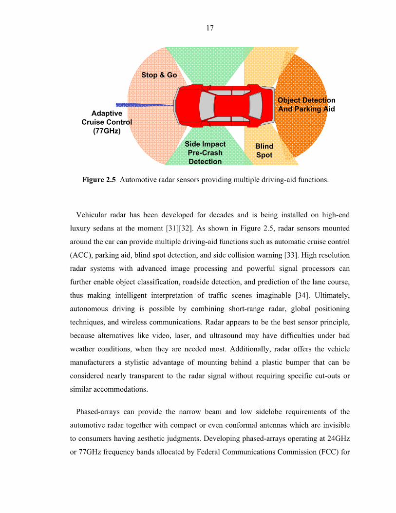
Vehicular radar has been developed for decades and is being installed on high-end
luxury sedans at the moment [31][32]. As shown in Figure 2.5, radar sensors mounted
around the car can provide multiple driving-aid functions such as automatic cruise control
(ACC), parking aid, blind spot detection, and side collision warning [33]. High resolution
radar systems with advanced image processing and powerful signal processors can
further enable object classification, roadside detection, and prediction of the lane course,
thus making intelligent interpretation of traffic scenes imaginable [34]. Ultimately,
autonomous driving is possible by combining short-range radar, global positioning
techniques, and wireless communications. Radar appears to be the best sensor principle,
because alternatives like video, laser, and ultrasound may have difficulties under bad
weather conditions, when they are needed most. Additionally, radar offers the vehicle
manufacturers a stylistic advantage of mounting behind a plastic bumper that can be
considered nearly transparent to the radar signal without requiring specific cut-outs or
similar accommodations.
Phased-arrays can provide the narrow beam and low sidelobe requirements of the
automotive radar together with compact or even conformal antennas which are invisible
to consumers having aesthetic judgments. Developing phased-arrays operating at 24GHz
or 77GHz frequency bands allocated by Federal Communications Commission (FCC) for
Object Detection And Parking Aid
Blind Spot
Side ImpactPre-Crash Detection
Adaptive Cruise Control
(77GHz)
Stop & Go
Figure 2.5 Automotive radar sensors providing multiple driving-aid functions.
18
vehicular radar applications is an intense research topic at the moment [31]-[40].
Radio astronomy is another important application area of phased-array. The next
generation radio telescope demands sensitivity one or two orders of magnitude higher
than current telescopes in use, requiring a total collecting aperture of approximately one
square kilometer [41]. Instead of using an ultra-giant single parabolic antenna, such a
system can be implemented with an array of more than one-hundred million small
antenna elements, providing additional benefits such as adaptive radio-interferences
rejection and multiple simultaneous beam formation.
Biomedication is an emerging yet promising application of phased-array. In [42], a
microwave imaging method is proposed using a phased-array to detect early-stage breast
cancer. The antenna array placed at the breast surface emits the wideband impulses
sequentially by each antenna. The beam-forming is employed at the receiver to focus the
backscattered signal from the malignant tumor and compensate for the frequency-
dependent propagation effect. The signal reflection is primarily due to the dielectric
discontinuity at the edge of the malignant tumors and the normal breast tissue. The
relevant contrast is an order of magnitude higher for microwave than for X-ray or
ultrasound [43], suggesting a much higher detection probability. Microwave imaging is
also a much cheaper solution than other current alternatives such as magnetic resonance
imaging (MRI) and is less harmful to the patients than X-ray. In [44], a hyperthermia
system is presented using a conformal phased-array to treat tumors in human limbs. The
array consists of 8 dipole radiators mounted on a cylindrical surface, focusing EM waves
to the tumor inside the limb to heat it to a higher temperature than surrounding tissues.
The thermal pattern can be varied by adjusting the amplitude and phase of each antenna
element. Tumors heated repeatedly to higher temperatures sometimes exhibit regression
and necrosis.
Phased-array electronic systems can also be applied to fields where the information
carrier is not EM waves, such as ultrasound imaging in biomedication [45] or sonar
system for underwater applications [46].
19
In summary, phased-array provides us with various ways to explore the space
dimension and take advantage of space diversity conveniently using electronic methods.
Its potential application range is only limited by the imagination of the engineers.
2.6 Phased-Array Architectures
2.6.1 Time Delay vs. Phase Shift
Phased-array is perhaps a misnomer for these systems given that true time delay, and
not phase shift, is required in each path for coherent addition of signals. As shown in
Figure 2.3, when a plane electromagnetic wave arrives at an antenna array at an angle of
α with respect to the normal to the array plane, the signal is received by each antenna at a
different time due to the difference in propagation path length. In general, an angle-
dependent time delay in each path at the receiver can compensate for the arrival delay
and effectively “listen” to a desired direction. In a one-dimensional array, the angle of
incidence, α, is related to the delay difference of two adjacent elements, τ, the spacing of
two adjacent antennas, D, and the speed of light, c, via
τα .)sin(. cD = (2.6)
The beam forming works independently of the frequency and bandwidth of the signal,
with ideal delay elements following each antenna. Unfortunately, there are practical
challenges to implement such broadband delay elements in the RF signal path, e.g., signal
attenuation, noise, and linearity degradation, as well as signal dispersion. Fortunately, in
many practical applications, particularly in wireless communications, the bandwidth of
interest is a small fraction of the center frequency, and hence a uniform delay (linear
phase) is only required over this narrow bandwidth. A simple way to realize the delay is
to approximate it with a constant phase shift (Figure 2.6). This aligns the carrier phase of
different paths. However, the modulating signal is not delayed appropriately, leading to
some dispersion in the demodulated signal creating inter-symbol interference (ISI).
Figure 2.7 graphically illustrates the mechanism by which the ISI is generated. Note that
the phase shift can be implemented in the LO, IF, or RF paths. Although mathematically
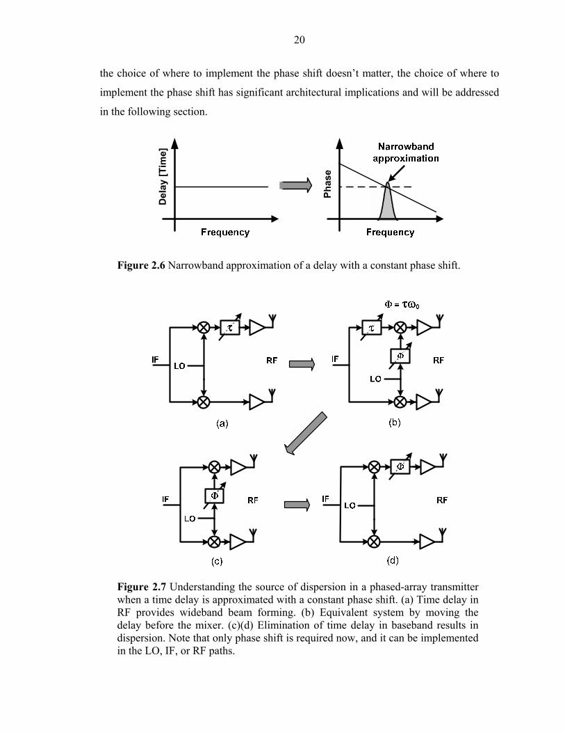
20
the choice of where to implement the phase shift doesn’t matter, the choice of where to
implement the phase shift has significant architectural implications and will be addressed
in the following section.
Del
ay [T
ime]
Phas
e
Figure 2.6 Narrowband approximation of a delay with a constant phase shift.
Figure 2.7 Understanding the source of dispersion in a phased-array transmitter when a time delay is approximated with a constant phase shift. (a) Time delay in RF provides wideband beam forming. (b) Equivalent system by moving the delay before the mixer. (c)(d) Elimination of time delay in baseband results in dispersion. Note that only phase shift is required now, and it can be implemented in the LO, IF, or RF paths.

21
2.6.2 Implementation of the Phase Shift: Choice of Architecture
Advances in silicon process technologies for integrated circuits have resulted in very
fast transistors with cut-off (unity current gain) frequencies above 200GHz. However,
transistor speed is only one of the parameters affecting the system operation. Additional
constraints imposed by the low breakdown voltages, losses of integrated passive elements,
low power budget, as well as cost and area constraints have important bearing on the
overall system performance. Therefore, the architecture of the phased-array system has to
be chosen carefully to ensure repeatability and reliability.
Ideally, broadband variable delays are needed to make the signals from all the paths
coherent before they are combined. Such a variable delay, if implemented in the signal
path at RF, can reduce power consumption. The gain of the delay stage should be
independent of the delay, as a change in amplitude with different delays will lead to
distortion when the signals are combined. Thus, the delay element should have large and
accurate variations in delay (0 to 140ps @ 24 GHz for an 8-element array, with spacing
of λ/2 between antennas) and low loss. However, implementing a broadband, low-loss,
true-time delay element at RF which is capable of large variation, occupies practical area,
and scales well with an increase in number of elements poses several problems.
As mentioned before, for narrowband signals, the delay can be approximated by a
phase shift. Figure 2.8 shows the different stages at which the phase shift can be
implemented in a simple two-element phased-array receiver example. In the signal path,
the phase shift can be provided at RF (Figure 2.8(a)), IF/baseband (Figure 2.8(b)), or
digitally (Figure 2.8(c)). Equivalently, the phase shift can also be provided by
downconverting the signal in each path with a phase-shifted LO signal (Figure 2.8(d)).
The selection of the architecture is accompanied, as always, by certain trade-offs in
power consumption, silicon area, and system reliability.
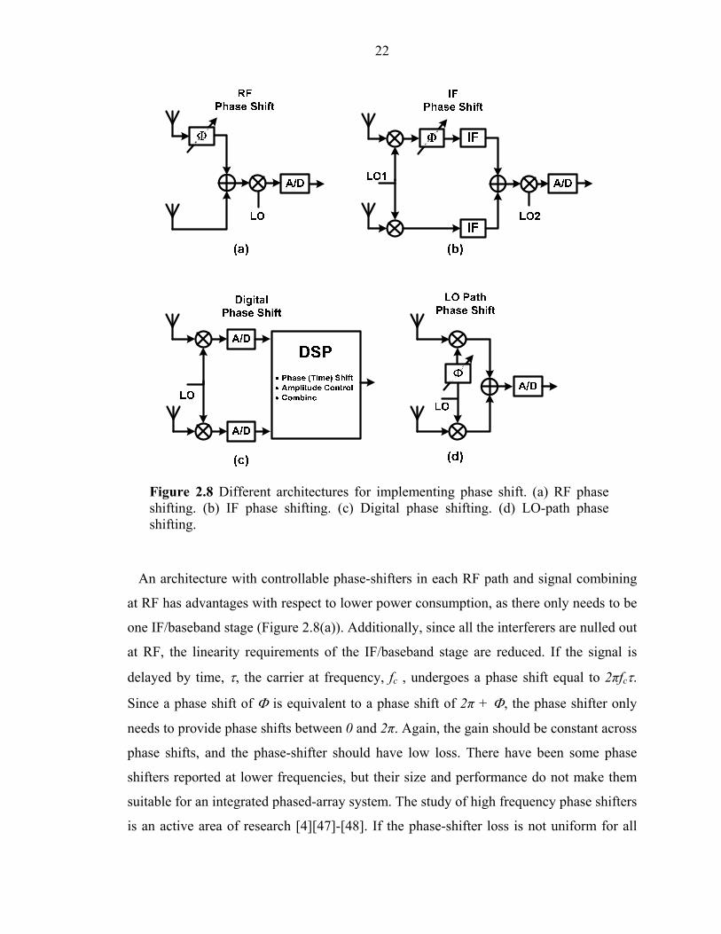
22
An architecture with controllable phase-shifters in each RF path and signal combining
at RF has advantages with respect to lower power consumption, as there only needs to be
one IF/baseband stage (Figure 2.8(a)). Additionally, since all the interferers are nulled out
at RF, the linearity requirements of the IF/baseband stage are reduced. If the signal is
delayed by time, τ, the carrier at frequency, fc , undergoes a phase shift equal to 2πfcτ.
Since a phase shift of Φ is equivalent to a phase shift of 2π + Φ, the phase shifter only
needs to provide phase shifts between 0 and 2π. Again, the gain should be constant across
phase shifts, and the phase-shifter should have low loss. There have been some phase
shifters reported at lower frequencies, but their size and performance do not make them
suitable for an integrated phased-array system. The study of high frequency phase shifters
is an active area of research [4][47]-[48]. If the phase-shifter loss is not uniform for all
Figure 2.8 Different architectures for implementing phase shift. (a) RF phase shifting. (b) IF phase shifting. (c) Digital phase shifting. (d) LO-path phase shifting.
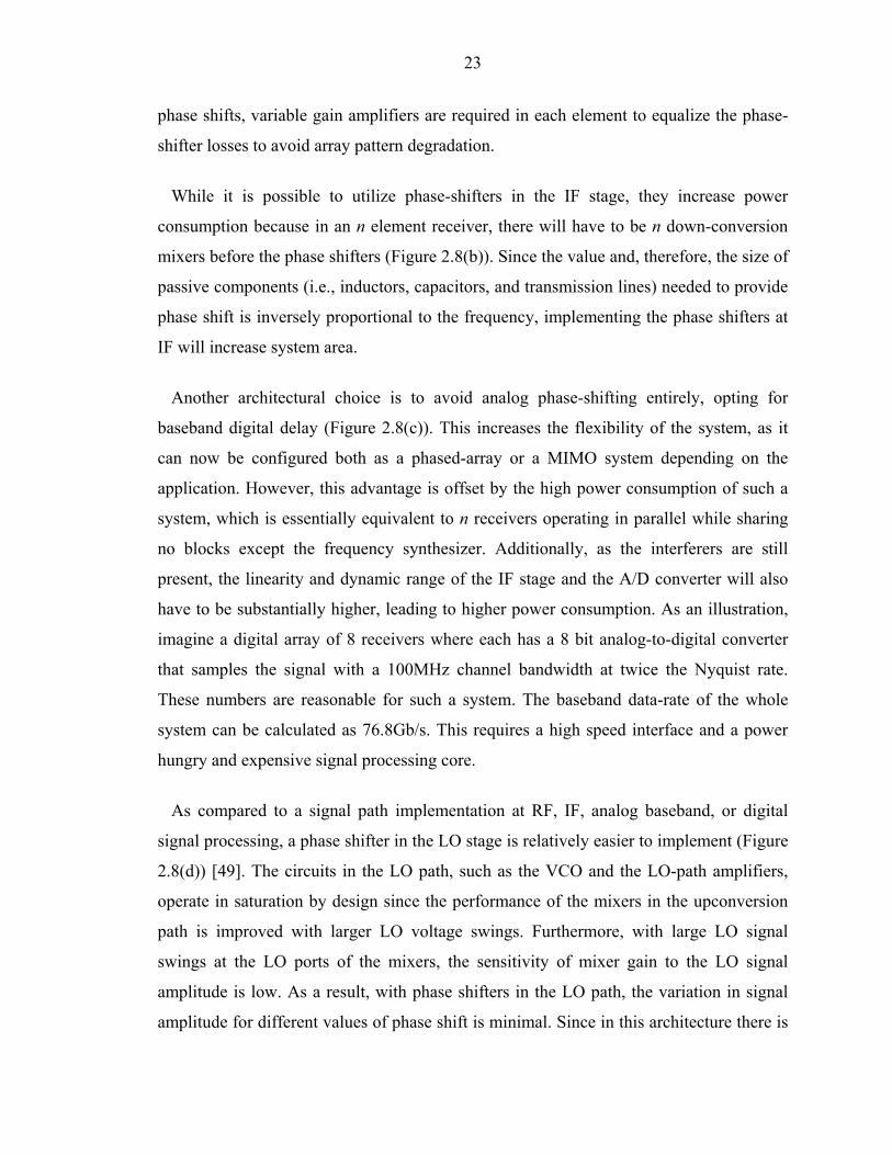
23
phase shifts, variable gain amplifiers are required in each element to equalize the phase-
shifter losses to avoid array pattern degradation.
While it is possible to utilize phase-shifters in the IF stage, they increase power
consumption because in an n element receiver, there will have to be n down-conversion
mixers before the phase shifters (Figure 2.8(b)). Since the value and, therefore, the size of
passive components (i.e., inductors, capacitors, and transmission lines) needed to provide
phase shift is inversely proportional to the frequency, implementing the phase shifters at
IF will increase system area.
Another architectural choice is to avoid analog phase-shifting entirely, opting for
baseband digital delay (Figure 2.8(c)). This increases the flexibility of the system, as it
can now be configured both as a phased-array or a MIMO system depending on the
application. However, this advantage is offset by the high power consumption of such a
system, which is essentially equivalent to n receivers operating in parallel while sharing
no blocks except the frequency synthesizer. Additionally, as the interferers are still
present, the linearity and dynamic range of the IF stage and the A/D converter will also
have to be substantially higher, leading to higher power consumption. As an illustration,
imagine a digital array of 8 receivers where each has a 8 bit analog-to-digital converter
that samples the signal with a 100MHz channel bandwidth at twice the Nyquist rate.
These numbers are reasonable for such a system. The baseband data-rate of the whole
system can be calculated as 76.8Gb/s. This requires a high speed interface and a power
hungry and expensive signal processing core.
As compared to a signal path implementation at RF, IF, analog baseband, or digital
signal processing, a phase shifter in the LO stage is relatively easier to implement (Figure
2.8(d)) [49]. The circuits in the LO path, such as the VCO and the LO-path amplifiers,
operate in saturation by design since the performance of the mixers in the upconversion
path is improved with larger LO voltage swings. Furthermore, with large LO signal
swings at the LO ports of the mixers, the sensitivity of mixer gain to the LO signal
amplitude is low. As a result, with phase shifters in the LO path, the variation in signal
amplitude for different values of phase shift is minimal. Since in this architecture there is
24
only one IF amplifier followed by two (I and Q) A/D converters the power consumption
is reduced as compared to an IF phase shift architecture.
2.6.3 Effects of Narrowband Approximation
As discussed in Section 2.6.1, the narrowband phase-shift approximation leads to some
signal distortion due to dispersion. The input signal that is distributed to each element in a
phased-array transmitter (or receiver) can be represented as ( ) ( ) ( )cos RFs t v t t tω φ= +⎡ ⎤⎣ ⎦ ,
where ( )v t and ( )tφ represent the baseband signal modulating the carrier. When phase
shifts are implemented in each element to achieve a radiation angle of θ for which the
propagation delay between successive elements differs by τ, the combined signal power is
( ) ( ) ( )1
0.cos
n
RFk
S t v t k t t kτ ω φ τ−
=
= − + −⎡ ⎤⎣ ⎦∑ . (2.7)
Thus, none of the phase-shifting architectures ensure that the baseband modulating
signals add up coherently, resulting in signal distortion. The signal degradation is
independent of the mechanism and/or the architecture used to produce the phase shift (RF
phase shift, LO phase shift, or IF/Baseband phase shift). The phase shifting approach
makes the carrier phase at different paths coherent, but due to the constant phase shift and,
hence, zero group delay, it does not synchronize the baseband modulation signals.
When the ratio of modulation bandwidth to carrier frequency increases, the signal
dispersion increases, manifested by the spreading of the constellation points. This
distortion results in a higher error vector magnitude (EVM) and results in an increased bit
error rate (BER) in wireless communication systems and in a reduced radial resolution in
radar applications. The EVM increases with an increase in the number of elements and/or
the bandwidth of the baseband signal and can be a source of error on both the transmitter
and the receiver side, leading to higher bit-error rates [50].
The effect of using phase shifting instead of true time delay compensation can be seen
in the simulation results shown in Figure 2.9(a) and (b). They show the simulated
25
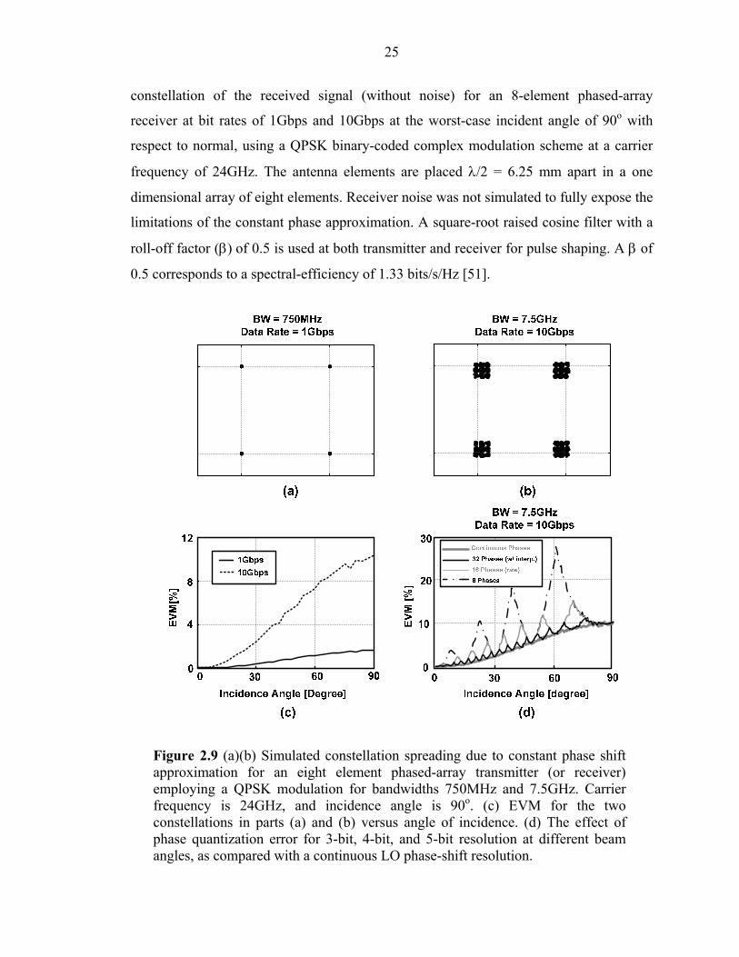
constellation of the received signal (without noise) for an 8-element phased-array
receiver at bit rates of 1Gbps and 10Gbps at the worst-case incident angle of 90o with
respect to normal, using a QPSK binary-coded complex modulation scheme at a carrier
frequency of 24GHz. The antenna elements are placed λ/2 = 6.25 mm apart in a one
dimensional array of eight elements. Receiver noise was not simulated to fully expose the
limitations of the constant phase approximation. A square-root raised cosine filter with a
roll-off factor (β) of 0.5 is used at both transmitter and receiver for pulse shaping. A β of
0.5 corresponds to a spectral-efficiency of 1.33 bits/s/Hz [51].
Figure 2.9 (a)(b) Simulated constellation spreading due to constant phase shift approximation for an eight element phased-array transmitter (or receiver) employing a QPSK modulation for bandwidths 750MHz and 7.5GHz. Carrier frequency is 24GHz, and incidence angle is 90o. (c) EVM for the two constellations in parts (a) and (b) versus angle of incidence. (d) The effect of phase quantization error for 3-bit, 4-bit, and 5-bit resolution at different beam angles, as compared with a continuous LO phase-shift resolution.
26
As the direction of the beam becomes more oblique, the delay between the paths
increases and so does the error introduced by constant phase-shift approximation. The
constellation spreading is a function of the incidence angle of the signal, ratio of signal-
bandwidth to carrier-frequency, and the pulse shaping used. Error vector magnitude
(EVM) is a measure of constellation spreading and is the root mean squared difference
between the perfectly demodulated signal and the distorted signal. The EVM of the
received signal was calculated for different signal bandwidths and angles of incidence,
and the results are plotted in Figure 2.9(c). This was done for a continuous phase control
at the LO. As can be seen, for a carrier of 24GHz, even for bit rates as high as 1Gbps and
an incidence angle of 90o (worst case), EVM is lower than 2%, and so the signal integrity
is maintained without additional equalization. Given the 250 MHz wireless
communication bandwidth, phase-shift of the carrier at 24 GHz (a BW/fcenter close to a
factor of 0.01) is a very good approximation for the delay and is sufficient for reliable
communication. However, for broadband communication or to achieve fine radial
resolutions in pulsed phased-array radars, it may be necessary to use a better
approximation of the actual delay rather than constant phase shift.
A phase shifter implementation in which the phase can be varied in discrete steps only
introduces additional dispersion for certain angles of incidence, as shown in Figure 2.9(d).
For example, in the phased-array transmitter described in Chapter 4, 16 discrete phases of
LO are interpolated to obtain 32 discrete phases (5-bit resolution) that are then used to
compensate the narrowband phase shift of the carrier frequency in each path. This
discrete method can only precisely compensate the carrier phase shift at 32 angles of
radiation between -90º and +90º. For all other angles, the signal constellation in each
transmit path is rotated by an angle equal to the phase quantization error, which depends
on the exact phase shift necessary in each path for the given angle of radiation. Since the
constellation for each transmit path is rotated differently, there will be interference
between the in-phase (I) and quadrature-phase (Q) demodulated channels at the receiver.
Figure 2.9(d) plots the simulated EVM as a function of the angle of incidence when
discrete phase shifts are used at the transmitter for 8, 16, and 32 available phases as well
as a continuous version (Figure 2.9(c)). The signal has a bandwidth of 7.5 GHz, and all
27
other simulation parameters are identical to those used in Figure 2.9(a) and (b). Using a
5-bit phase shifting scheme with phase steps of 5.6o causes a peak EVM of 12% at a
radiation angle of 75o, which is only 1.14 times larger than the peak EVM generated with
continuous phase shifting. In the latter case, the peak naturally happens at the radiation
angle of 90o, which corresponds to largest time delay between antennas. It is evident
from Figure 2.9(d) that a 3-bit phase shifting resolution results in a much larger EVM
relative to a 5-bit phase resolution. If a 3-bit phase shifting scheme with 45o phase steps
were used, this peak would occur at a radiation angle of 60o, with a peak EVM value
which is 180% higher than the peak EVM value for a continuous version. The relative
extra degradation due to a coarse phase resolution increases for lower bandwidth-to-
carrier ratios.
A higher-resolution phase shifter in RF or LO paths is also preferable because it
provides more accurate beamforming and lower sidelobe levels. A low-resolution phase
shifter introduces a gain loss due to phase quantization [52]. If an N-bit phase shifter is
used, assuming a uniform spread of phases across the array, the gain loss due to phase
quantization is given by
⎟⎠
⎞⎜⎝
⎛== ∫ N
NN N
dlossonquantizati2πsin
π2cos
π2 2π
0θθ . (2.8)
Table 2.1 shows the resulting gain loss due to phase quantization. Using only 3 bits of
resolution for the phase shifter this gain loss can be reduced to 0.22dB, which is
negligible. Therefore the major effect of phase quantization is causing dispersion
depicted in Fig. 2.11, which as discussed in next section in an OFDM system can be
further reduced by a one-tap equalizer.
28
Table 2.1 Gain loss due to phase shifter quantization.
2.6.4 Using OFDM to Remedy the Error Caused by the Constant Phase Shift
Approximation
A method to mitigate the deterministic errors caused by the phase-shift approximation
is to use a normalized orthogonal frequency division multiplexing (OFDM) modulation
scheme for the baseband input that is distributed to all the elements in the transmitter [53].
For a QPSK signal at data rate R bps, the time period of each symbol is 12sT
R= .
Therefore, the complex digital baseband signal is ( ) where is complexd s n ns nT b b= . In
OFDM, the total bandwidth of the system is divided into Nc channels, with the Nc sub-
carriers orthogonal. The baseband digital data is divided into Nc parallel streams, each of
which is used to modulate a sub-carrier [54]. Thus, each OFDM symbol consists of Nc
QPSK symbols, and for each frame (of duration NcTs)
( ).1 .2 .
0.
cc
k nN jN
d s kk
s nT b eπ−
=
= ∑ . (2.9)
Since each of the channels in the OFDM scheme is narrowband, the error due to the
time delay being replaced by a constant phase-shift can be largely corrected by
multiplying the input modulating each sub-carrier by a complex normalizing factor, αk,
such that
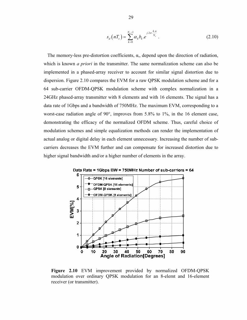
29
( ).1 .2 .
0.
cc
k nN jN
d s k kk
s nT b eπ
α−
=
= ∑ . (2.10)
The memory-less pre-distortion coefficients, αk, depend upon the direction of radiation,
which is known a priori in the transmitter. The same normalization scheme can also be
implemented in a phased-array receiver to account for similar signal distortion due to
dispersion. Figure 2.10 compares the EVM for a raw QPSK modulation scheme and for a
64 sub-carrier OFDM-QPSK modulation scheme with complex normalization in a
24GHz phased-array transmitter with 8 elements and with 16 elements. The signal has a
data rate of 1Gbps and a bandwidth of 750MHz. The maximum EVM, corresponding to a
worst-case radiation angle of 90°, improves from 5.8% to 1%, in the 16 element case,
demonstrating the efficacy of the normalized OFDM scheme. Thus, careful choice of
modulation schemes and simple equalization methods can render the implementation of
actual analog or digital delay in each element unnecessary. Increasing the number of sub-
carriers decreases the EVM further and can compensate for increased distortion due to
higher signal bandwidth and/or a higher number of elements in the array.
EVM
[%]
Figure 2.10 EVM improvement provided by normalized OFDM-QPSK modulation over ordinary QPSK modulation for an 8-elemt and 16-element receiver (or transmitter).
30
2.7 Wireless Communication at Millimeter-Wave Frequencies
Larger available bandwidth and smaller physical system size motivate a move to high
frequencies for wireless communications. In this section, the tradeoffs of wireless
communication at millimeter-wave frequencies are discussed, with an emphasis on
phased-array systems.
The beamforming and electronic beam-steering properties of phased-arrays provide a
solution to the demand for directional wireless links at high frequencies. Resonance-
based planar antennas such as dipoles or patch antennas are well-suited for an integrated
phased-array based system with electronic beam steering. A typical patch antenna array
at 24GHz, for instance, has an antenna gain of 8dB [55]. According to the antenna
theorem, the aperture area of an antenna, for a given gain, decreases with an increase in
frequency, reducing the power collected at the receiver at high frequencies [56]. The
collected power cannot be increased by increasing aperture area, as that increases antenna
gain, making the antenna more directional and hence limiting the angles at which
radiation is possible. Thus, in a resonance-antenna based communication system, the
advantage of large bandwidths at high frequencies is offset to some extent by the lower
received power and the higher receiver noise figure at high frequencies. A quantitative
analysis of this trade-off is detailed in this section.
For a transmit EIRP of PTX, the signal power at the receiver, PRX, is given by Friis’
equation [57] :
( )
2
4TX RX
RX TX l
G GP P
dλ
π= , (2.11)
where GTX, GRX are receiver and transmitter antenna gain, λ is the wavelength, d is the
distance between the transmitter and receiver, and l is the exponent, which can be higher
than the nominal value of two to account for excess path loss. In order to explore the
tradeoffs of moving to high frequencies, the channel capacity C (in bps), given by
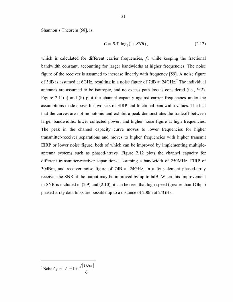
31
Shannon’s Theorem [58], is
2.log (1 )C BW SNR= + , (2.12)
which is calculated for different carrier frequencies, fc, while keeping the fractional
bandwidth constant, accounting for larger bandwidths at higher frequencies. The noise
figure of the receiver is assumed to increase linearly with frequency [59]. A noise figure
of 3dB is assumed at 6GHz, resulting in a noise figure of 7dB at 24GHz.2 The individual
antennas are assumed to be isotropic, and no excess path loss is considered (i.e., l=2).
Figure 2.11(a) and (b) plot the channel capacity against carrier frequencies under the
assumptions made above for two sets of EIRP and fractional bandwidth values. The fact
that the curves are not monotonic and exhibit a peak demonstrates the tradeoff between
larger bandwidths, lower collected power, and higher noise figure at high frequencies.
The peak in the channel capacity curve moves to lower frequencies for higher
transmitter-receiver separations and moves to higher frequencies with higher transmit
EIRP or lower noise figure, both of which can be improved by implementing multiple-
antenna systems such as phased-arrays. Figure 2.12 plots the channel capacity for
different transmitter-receiver separations, assuming a bandwidth of 250MHz, EIRP of
30dBm, and receiver noise figure of 7dB at 24GHz. In a four-element phased-array
receiver the SNR at the output may be improved by up to 6dB. When this improvement
in SNR is included in (2.9) and (2.10), it can be seen that high-speed (greater than 1Gbps)
phased-array data links are possible up to a distance of 200m at 24GHz.
2 Noise figure:
[ ]6
1HzGf
F +=
32
(a)
(b)
Figure 2.11 Comparison of channel capacities for different system parameters demonstrate the tradeoffs of moving to high frequencies. (a) Channel capacity for EIRP = 0.1W, BW = 4%. (b) Channel capacity for EIRP = 1W, BW = 1% [53].
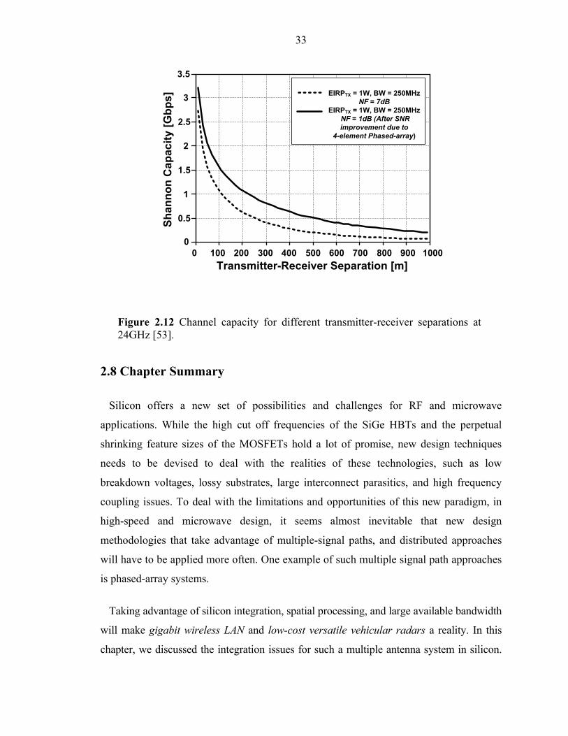
33
Transmitter-Receiver Separation [m]
Shan
non
Cap
acity
[Gbp
s]
0 100 200 300 400 500 600 700 800 900 10000
3.5
0.5
1
1.5
2
2.5
3 EIRPTX = 1W, BW = 250MHzNF = 7dB
EIRPTX = 1W, BW = 250MHz NF = 1dB (After SNR improvement due to
4-element Phased-array)
Figure 2.12 Channel capacity for different transmitter-receiver separations at 24GHz [53].
2.8 Chapter Summary
Silicon offers a new set of possibilities and challenges for RF and microwave
applications. While the high cut off frequencies of the SiGe HBTs and the perpetual
shrinking feature sizes of the MOSFETs hold a lot of promise, new design techniques
needs to be devised to deal with the realities of these technologies, such as low
breakdown voltages, lossy substrates, large interconnect parasitics, and high frequency
coupling issues. To deal with the limitations and opportunities of this new paradigm, in
high-speed and microwave design, it seems almost inevitable that new design
methodologies that take advantage of multiple-signal paths, and distributed approaches
will have to be applied more often. One example of such multiple signal path approaches
is phased-array systems.
Taking advantage of silicon integration, spatial processing, and large available bandwidth
will make gigabit wireless LAN and low-cost versatile vehicular radars a reality. In this
chapter, we discussed the integration issues for such a multiple antenna system in silicon.

34
In the rest of this thesis, the first silicon-based phased-array transmitters demonstrated at
two different frequency bands (24GHz and 77GHz) and with different architectures
suitable for each application will be presented.
35
Chapter 3 A 24GHz, +14.5dBm Fully-Integrated Power Amplifier in 0.18μm CMOS
A 24GHz, +14.5dBm Fully-Integrated Power Amplifier in 0.18μm CMOS
The quest for multi-Gigabit-per-second data rates in wireless networks has generated
interest in the large bandwidth available at high frequencies. The Industrial, Scientific,
and Medical (ISM) band at 24GHz has emerged as a viable candidate for gigabit-per-
second wireless network solutions [36]. The allocation of the 22-29GHz band for
wireless vehicular radar applications has added to the attractiveness of the frequency
spectrum around 24GHz [35]. As a result, research on 24GHz band wireless technologies
has accelerated, with receiver building blocks being demonstrated in GaAs pHEMPT [55]
and SiGe BiCMOS [33][37]. A fully-integrated eight-element phased-array receiver in
SiGe has also been reported at this frequency [60]. The implementation of these high-
frequency systems in CMOS technologies will enable unprecedented levels of integration,
making it possible to realize new architectures that combine microwave, analog, and
digital circuitry on the same substrate at low cost. While there have been some recent
efforts to implement building blocks above 20GHz on CMOS processes [61]-[64], the
power amplifier (PA) reported in this chapter, and the fully-integrated four-element
phased-array transmitter described in Chapter 4, represent the first efforts to integrate a
complete multi-element transmitter with on-chip PAs in a CMOS process at 24GHz.
In Section 3.1 challenges of implementing on-chip power amplifiers in a CMOS
technology are discussed. In Section 3.2, we calculate the output power required at
24GHz for two applications, namely wireless point-to-point communication and short-
range radar. Section 3.3 details the design of the amplifier and transmission-line-based
36
matching networks, followed by the measurement results presented in Section 3.4.
Section 3.5 summarizes the results of this work.
3.1 Introduction
An integrated CMOS power amplifier at 24GHz presents several challenges. The two
most important issues are the low unity power gain frequency, fmax,, of MOS transistors,
and the loss of on-chip passive elements, such as inductors and transmission lines,
required for impedance matching. For narrowband amplifiers, where device capacitance
is normally tuned out, fmax is a better metric for device speed than fT. In MOSFETs, fmax is
limited primarily by the series gate resistance [64][65]. Generally, MOS transistors have
lower fT and fmax as compared to SiGe bipolar transistors fabricated with the same feature
size [66]. In the 0.18μm process used in this design, the NMOS transistors, with an
optimum layout, have an fmax of 65GHz, which is almost a factor of two smaller than the
fmax of their SiGe bipolar counterparts.
Lossy on-chip passives present another barrier to the full integration of a high-
frequency PA. Skin effect results in larger ohmic losses in inductors and transmission
lines at high frequencies. The skin depth in Aluminum at 24GHz is 0.5μm, which negates
some of the advantages of a thick top metal layer, though the lateral sidewalls still help in
reducing loss. Although Copper has better conductivity, in practice its performance can
be additionally degraded by the cheese and fill rules necessary for stress relief during
fabrication. As an example the cheese rule can increase the sheet resistance of a thick
copper trace by a factor of two. Due to the relatively high conductivity of the substrate in
most CMOS processes, the inductors and coplanar waveguide transmission line structures
have substrate-induced losses as well. The combination of low active gain at high
frequencies and high loss in impedance matching networks reduces the power gain of a
single-stage amplifier. As a result, it becomes necessary to cascade an impractically large
number of amplifier stages to achieve desired output power levels.
In this design, a substrate-shielded coplanar waveguide structure is implemented that
effectively lowers substrate loss and reduces on-chip wavelength. This is an enhanced
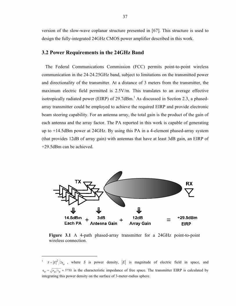
37
version of the slow-wave coplanar structure presented in [67]. This structure is used to
design the fully-integrated 24GHz CMOS power amplifier described in this work.
3.2 Power Requirements in the 24GHz Band
The Federal Communications Commission (FCC) permits point-to-point wireless
communication in the 24-24.25GHz band, subject to limitations on the transmitted power
and directionality of the transmitter. At a distance of 3 meters from the transmitter, the
maximum electric field permitted is 2.5V/m. This translates to an average effective
isotropically radiated power (EIRP) of 29.7dBm.1 As discussed in Section 2.3, a phased-
array transmitter could be employed to achieve the required EIRP and provide electronic
beam steering capability. For an antenna array, the total gain is the product of the gain of
each antenna and the array factor. The PA reported in this work is capable of generating
up to +14.5dBm power at 24GHz. By using this PA in a 4-element phased-array system
(that provides 12dB of array gain) with antennas that have at least 3dB gain, an EIRP of
+29.5dBm can be achieved.
Figure 3.1 A 4-path phased-array transmitter for a 24GHz point-to-point wireless connection.
1 o2η2ES = , where S is power density, E is magnitude of electric field in space, and
377Ωooo ≈= εμη is the characteristic impedance of free space. The transmitter EIRP is calculated by integrating this power density on the surface of 3-meter-radius sphere.
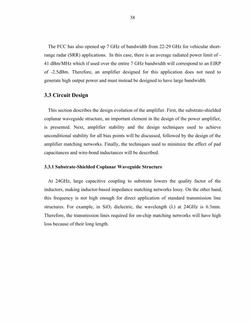
38
The FCC has also opened up 7 GHz of bandwidth from 22-29 GHz for vehicular short-
range radar (SRR) applications. In this case, there is an average radiated power limit of -
41 dBm/MHz which if used over the entire 7 GHz bandwidth will correspond to an EIRP
of -2.5dBm. Therefore, an amplifier designed for this application does not need to
generate high output power and must instead be designed to have large bandwidth.
3.3 Circuit Design
This section describes the design evolution of the amplifier. First, the substrate-shielded
coplanar waveguide structure, an important element in the design of the power amplifier,
is presented. Next, amplifier stability and the design techniques used to achieve
unconditional stability for all bias points will be discussed, followed by the design of the
amplifier matching networks. Finally, the techniques used to minimize the effect of pad
capacitances and wire-bond inductances will be described.
3.3.1 Substrate-Shielded Coplanar Waveguide Structure
At 24GHz, large capacitive coupling to substrate lowers the quality factor of the
inductors, making inductor-based impedance matching networks lossy. On the other hand,
this frequency is not high enough for direct application of standard transmission line
structures. For example, in SiO2 dielectric, the wavelength (λ) at 24GHz is 6.3mm.
Therefore, the transmission lines required for on-chip matching networks will have high
loss because of their long length.
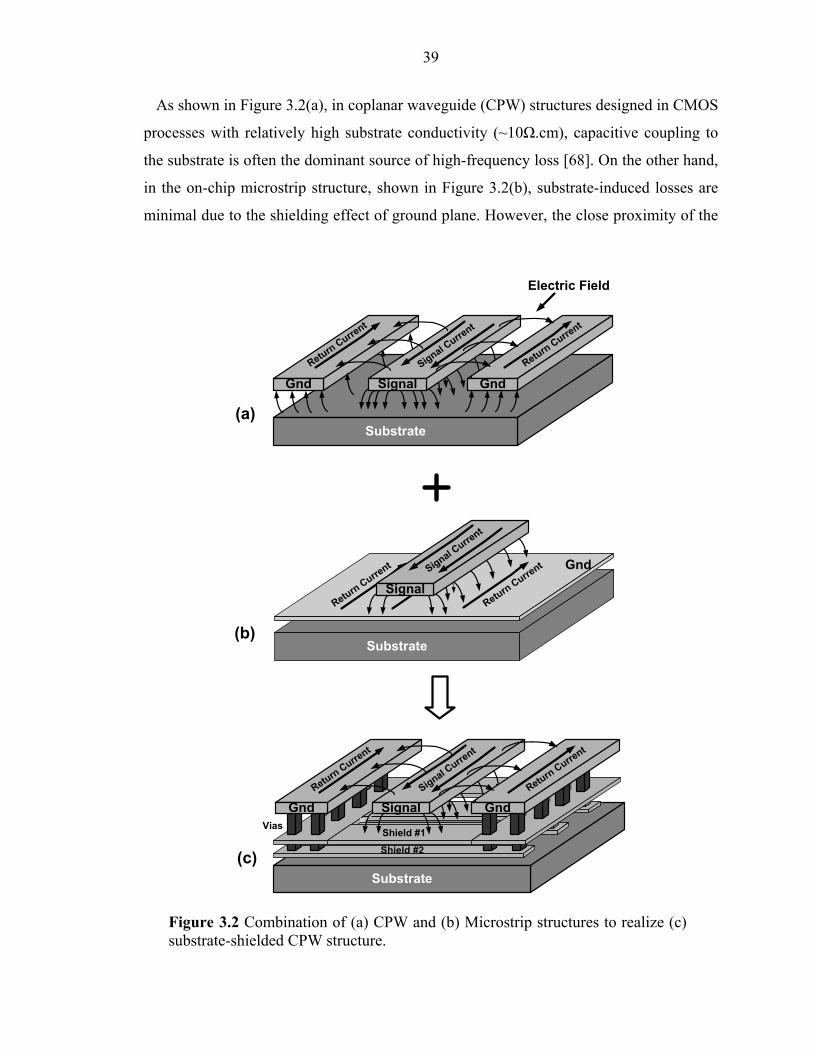
39
As shown in Figure 3.2(a), in coplanar waveguide (CPW) structures designed in CMOS
processes with relatively high substrate conductivity (~10Ω.cm), capacitive coupling to
the substrate is often the dominant source of high-frequency loss [68]. On the other hand,
in the on-chip microstrip structure, shown in Figure 3.2(b), substrate-induced losses are
minimal due to the shielding effect of ground plane. However, the close proximity of the
Substrate
00
00
Substrate
Electric Field
Gnd
Substrate
Gnd Signal Gnd
Vias
Signal Curre
nt
Return Current
Return Current
Return Current
SignalSignal C
urrent
Return Current
(b)
(a)
(c)
Gnd Signal Gnd
Shield #1
Signal Curre
nt
Return Current
Return Current
Shield #2
Figure 3.2 Combination of (a) CPW and (b) Microstrip structures to realize (c) substrate-shielded CPW structure.
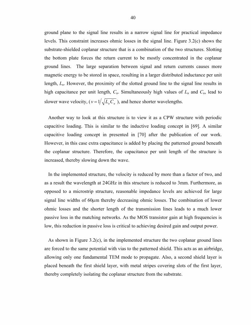
40
ground plane to the signal line results in a narrow signal line for practical impedance
levels. This constraint increases ohmic losses in the signal line. Figure 3.2(c) shows the
substrate-shielded coplanar structure that is a combination of the two structures. Slotting
the bottom plate forces the return current to be mostly concentrated in the coplanar
ground lines. The large separation between signal and return currents causes more
magnetic energy to be stored in space, resulting in a larger distributed inductance per unit
length, Lu. However, the proximity of the slotted ground line to the signal line results in
high capacitance per unit length, Cu. Simultaneously high values of Lu and Cu, lead to
slower wave velocity, ( uuCLv 1= ), and hence shorter wavelengths.
Another way to look at this structure is to view it as a CPW structure with periodic
capacitive loading. This is similar to the inductive loading concept in [69]. A similar
capacitive loading concept in presented in [70] after the publication of our work.
However, in this case extra capacitance is added by placing the patterned ground beneath
the coplanar structure. Therefore, the capacitance per unit length of the structure is
increased, thereby slowing down the wave.
In the implemented structure, the velocity is reduced by more than a factor of two, and
as a result the wavelength at 24GHz in this structure is reduced to 3mm. Furthermore, as
opposed to a microstrip structure, reasonable impedance levels are achieved for large
signal line widths of 60μm thereby decreasing ohmic losses. The combination of lower
ohmic losses and the shorter length of the transmission lines leads to a much lower
passive loss in the matching networks. As the MOS transistor gain at high frequencies is
low, this reduction in passive loss is critical to achieving desired gain and output power.
As shown in Figure 3.2(c), in the implemented structure the two coplanar ground lines
are forced to the same potential with vias to the patterned shield. This acts as an airbridge,
allowing only one fundamental TEM mode to propagate. Also, a second shield layer is
placed beneath the first shield layer, with metal stripes covering slots of the first layer,
thereby completely isolating the coplanar structure from the substrate.
41
3.3.2 Characterization of the Substrate-Shielded CPW Structure
The simulated electric and magnetic fields of a cross-section of the substrate-shielded
CPW structure with and without slotted shields is shown in Figure 3.3. In the shielded
structure the electric fields do not penetrate into the substrate, reducing capacitively-
coupled substrate losses. Though the penetration of the magnetic field into the substrate is
not affected by the presence of the shield, EM simulations indicate that this does not
contribute significantly to the loss as the eddy currents are limited.
To characterize the substrate-shielded CPW structure, a separate test structure was
fabricated in the same process as the amplifier. The test structure was designed for a
characteristic impedance of 27.5Ω, the same impedance used for impedance-matching in
Figure 3.3 Electric and Magnetic field distributions from 3D EM simulations of (a), (b) a normal CPW structure, and (c), (d) a substrate-shielded CPW structure.
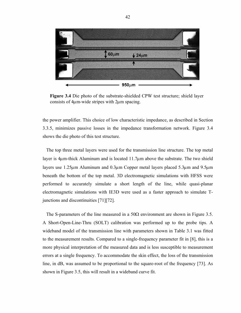
42
the power amplifier. This choice of low characteristic impedance, as described in Section
3.3.5, minimizes passive losses in the impedance transformation network. Figure 3.4
shows the die photo of this test structure.
The top three metal layers were used for the transmission line structure. The top metal
layer is 4μm-thick Aluminum and is located 11.7μm above the substrate. The two shield
layers use 1.25μm Aluminum and 0.3μm Copper metal layers placed 5.3μm and 9.5μm
beneath the bottom of the top metal. 3D electromagnetic simulations with HFSS were
performed to accurately simulate a short length of the line, while quasi-planar
electromagnetic simulations with IE3D were used as a faster approach to simulate T-
junctions and discontinuities [71][72].
The S-parameters of the line measured in a 50Ω environment are shown in Figure 3.5.
A Short-Open-Line-Thru (SOLT) calibration was performed up to the probe tips. A
wideband model of the transmission line with parameters shown in Table 3.1 was fitted
to the measurement results. Compared to a single-frequency parameter fit in [8], this is a
more physical interpretation of the measured data and is less susceptible to measurement
errors at a single frequency. To accommodate the skin effect, the loss of the transmission
line, in dB, was assumed to be proportional to the square-root of the frequency [73]. As
shown in Figure 3.5, this will result in a wideband curve fit.
Figure 3.4 Die photo of the substrate-shielded CPW test structure; shield layer consists of 4μm-wide stripes with 2μm spacing.

43
Table 3.1 Simulated and measured parameters of the transmission line at 24GHz with wideband fitting.
Figure 3.5 Simulated and measured S-parameters of the transmission line. (a) Reflection parameter (S11) and (b) Transmission parameter (S21).
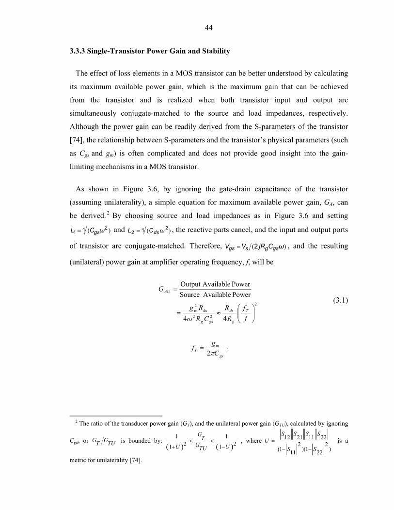
44
3.3.3 Single-Transistor Power Gain and Stability
The effect of loss elements in a MOS transistor can be better understood by calculating
its maximum available power gain, which is the maximum gain that can be achieved
from the transistor and is realized when both transistor input and output are
simultaneously conjugate-matched to the source and load impedances, respectively.
Although the power gain can be readily derived from the S-parameters of the transistor
[74], the relationship between S-parameters and the transistor’s physical parameters (such
as Cgs and gm) is often complicated and does not provide good insight into the gain-
limiting mechanisms in a MOS transistor.
As shown in Figure 3.6, by ignoring the gate-drain capacitance of the transistor
(assuming unilaterality), a simple equation for maximum available power gain, GA, can
be derived. 2 By choosing source and load impedances as in Figure 3.6 and setting
)( 21 1 ωCL gs= and )( 2
2 1 ωCL ds= , the reactive parts cancel, and the input and output ports
of transistor are conjugate-matched. Therefore, )( ωCjRVV gsgsgs 2= , and the resulting
(unilateral) power gain at amplifier operating frequency, f, will be
2
2gs
2ds
2m
44
PowerAvailableSourcePowerAvailableOutput
⎟⎟⎠
⎞⎜⎜⎝
⎛≈=
=
ff
RR
CRωRg
G
T
g
ds
g
AU
(3.1)
gs
mT C
gfπ2
= .
2 The ratio of the transducer power gain (GT), and the unilateral power gain (GTU), calculated by ignoring
Cgd, or TUGTG is bounded by: ( ) ( )21
121
1
UTUGTG
U −<<
+, where
)2
221)(2
111(
22112112
SS
SSSSU
−−= is a
metric for unilaterality [74].
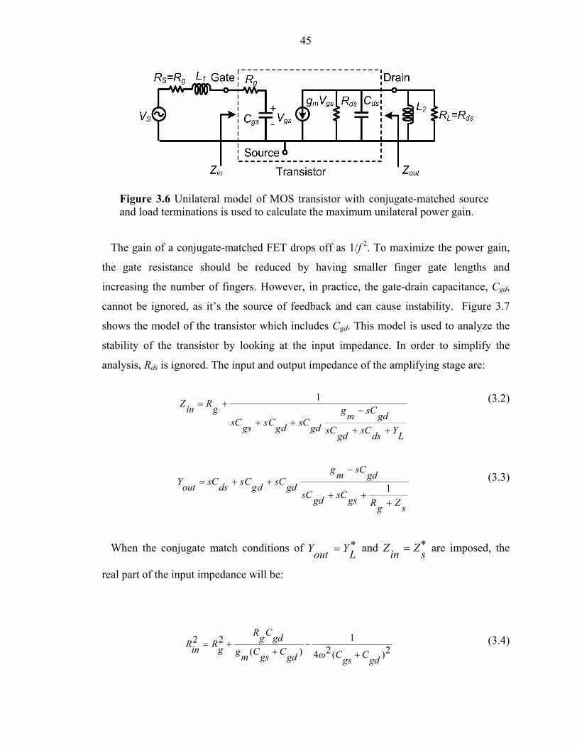
45
Figure 3.6 Unilateral model of MOS transistor with conjugate-matched source and load terminations is used to calculate the maximum unilateral power gain.
The gain of a conjugate-matched FET drops off as 1/f 2. To maximize the power gain,
the gate resistance should be reduced by having smaller finger gate lengths and
increasing the number of fingers. However, in practice, the gate-drain capacitance, Cgd,
cannot be ignored, as it’s the source of feedback and can cause instability. Figure 3.7
shows the model of the transistor which includes Cgd. This model is used to analyze the
stability of the transistor by looking at the input impedance. In order to simplify the
analysis, Rds is ignored. The input and output impedance of the amplifying stage are:
1
LYdssCgdsCgdsCmg
gdsCdgCsgssCgRinZ
++
−++
+= (3.2)
sZgRgssCgdsC
gdsCmg
gdsCdgCsdssCoutY
+++
−++=
1 (3.3)
When the conjugate match conditions of ∗= LYoutY and ∗= sΖinΖ are imposed, the
real part of the input impedance will be:
2)(24
1)(
22
gdCgsCωgdCgsCmggdCgR
gRinR+
−+
+= (3.4)
46
Since the right side of the Equation (3.4) has a negative component, in order to be able
to have input conjugate match the following condition should hold:
1
2
<<=
>
gs
gd
m
Tg
CC
fgfR
α
(3.5)
Therefore for having an amplifier with a power-matched input Rg should be comparable
to mg1 of the transistor. A more detailed analysis shows that for small values of Rg , the
presence of feedback capacitor Cgd can make the amplifier unstable. Equations (3.1) and
(3.5) demonstrate the conflicting requirements that arise when a single transistor is used
as the amplifying element. As can be seen from Equation (3.5), in order to maximize the
power gain through maximum power transfer to the transistor, Rg should be large, in
which case the power gain of the transistor will be significantly reduced as per Equation
(3.1). This conflict can be resolved by using a cascode design for the amplifying stages.
3.3.4 Stability of the Cascode Pair
As discussed in the previous section, a single MOS transistor designed for maximum
power gain in a common source configuration and conjugate matched at input and output
can be unstable. At 24GHz, this is true for the 0.18μm CMOS transistors used in the
design of the 24GHz PA. The cascode structure makes the device more unilateral, and
Rg
Cgs Vgs+-
gmVgs
Transistor
Cds
Zin Zout
ZS YL
CgdGate Drain
Source
Figure 3.7 Model of MOS amplifier used to derive stability criterion.
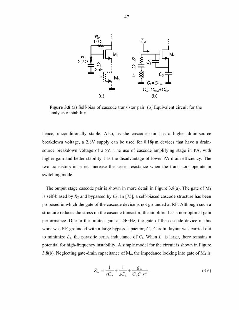
47
hence, unconditionally stable. Also, as the cascode pair has a higher drain-source
breakdown voltage, a 2.8V supply can be used for 0.18μm devices that have a drain-
source breakdown voltage of 2.5V. The use of cascode amplifying stage in PA, with
higher gain and better stability, has the disadvantage of lower PA drain efficiency. The
two transistors in series increase the series resistance when the transistors operate in
switching mode.
The output stage cascode pair is shown in more detail in Figure 3.8(a). The gate of M4
is self-biased by R2 and bypassed by C1. In [75], a self-biased cascode structure has been
proposed in which the gate of the cascode device is not grounded at RF. Although such a
structure reduces the stress on the cascode transistor, the amplifier has a non-optimal gain
performance. Due to the limited gain at 24GHz, the gate of the cascode device in this
work was RF-grounded with a large bypass capacitor, C1. Careful layout was carried out
to minimize L1, the parasitic series inductance of C1. When L1 is large, there remains a
potential for high-frequency instability. A simple model for the circuit is shown in Figure
3.8(b). Neglecting gate-drain capacitance of M4, the impedance looking into gate of M4 is
23232
11sCC
gsCsC
Z min ++= . (3.6)
Figure 3.8 (a) Self-bias of cascode transistor pair. (b) Equivalent circuit for the analysis of stability.
48
The real part of this impedance has a negative component equal to )(- 232 ωCCgm ,
indicating that the circuit can oscillate if there is a parasitic inductance between the gate
and ground. By introducing the series resistance R1, the circuit can be stabilized. The
value of R1 is chosen such that the amplifier remains stable for the largest estimated value
of L1. Using (3.6), the condition for the stability can be expressed as
2osc32
1C ωCg
R m> (3.7)
1
3211
111 , 1 −
⎟⎟⎠
⎞⎜⎜⎝
⎛++==
CCCC
CLω eq
eqosc .
For parasitic inductances up to 100pH, by placing a 2.7Ω series resistance the amplifier
will be unconditionally stable.
3.3.5 Amplifier Design
The 24GHz power amplifier shown in Figure 3.9 is a single-ended two-stage design
that can directly feed a single-ended 50Ω antenna, thereby making a Balun or a
differential antenna unnecessary. If a differential antenna is available, two amplifiers in
parallel can produce 3dB higher output power similar to [76][77].
The PA is designed to operate in class AB mode. The transistor fmax is just 65GHz, so
the harmonic content at the drain of the transistor for the 24GHz input signal is low.
Therefore, amplifier classes based on harmonic matching such as class E and class F will
not increase the amplifier efficiency significantly.
To minimize the effect of gate series resistance, Rg , which can be the limiting factor for
fmax, the finger width of transistors was chosen to be 2μm, with gate contacts at both ends.
This also allows substrate contacts to be placed closer to the device, minimizing substrate
losses in transistor.

49
As shown in Figure 3.9, the stages are designed such that all the phase shifts provided
by transmission lines required for impedance matching are small. The output stage
matching is designed to convert the 50Ω antenna impedance to the proper impedance at the
drain of M4, maximizing output power and efficiency. This proper impedance is chosen by
the load pull simulation of the cascode pair when the gate of the input transistor is driven
by a large-signal source. As shown in Figure 3.10, Ts brings down the 50Ω antenna
impedance to achieve higher output power, while Tp acts as a shorted-stub inductor to
resonate drain-substrate capacitance of M4. Inter-stage matching is designed to achieve
optimum impedance at the drain of the cascoded transistor, while input matching is
designed to ensure a good power match for large input signal amplitudes.
For minimum passive loss, the output stage characteristic impedance should be lower
than the inter-stage one, but to simplify the design and test procedures a single
characteristic impedance of 27.5Ω was used for the transmission lines across the chip. A
weighted least-mean-square (LMS) optimization with gradient-descent scheme was used
to choose this characteristic impedance and all the transmission line lengths. All 2pF
MIM capacitors used to short parallel stubs have a high width-to-length ratio to make the
electrical length of the shorted stubs more accurate.
Figure 3.9 Schematic of the 24GHz, 14.5dBm fully-integrated CMOS power amplifier.
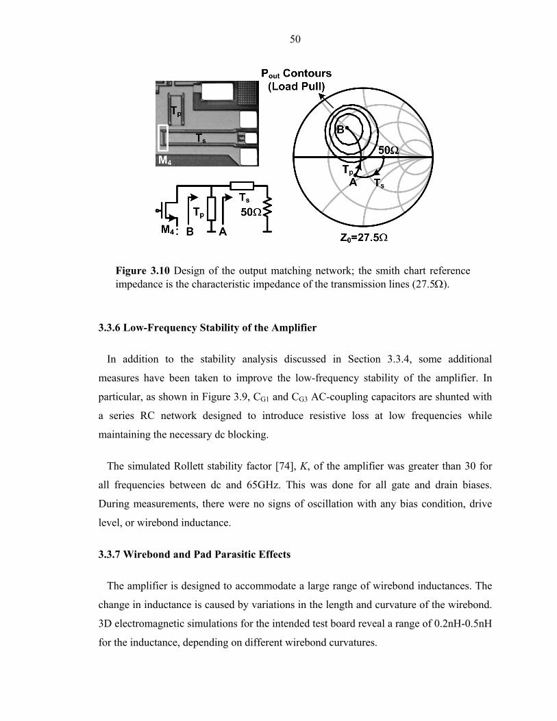
50
3.3.6 Low-Frequency Stability of the Amplifier
In addition to the stability analysis discussed in Section 3.3.4, some additional
measures have been taken to improve the low-frequency stability of the amplifier. In
particular, as shown in Figure 3.9, CG1 and CG3 AC-coupling capacitors are shunted with
a series RC network designed to introduce resistive loss at low frequencies while
maintaining the necessary dc blocking.
The simulated Rollett stability factor [74], K, of the amplifier was greater than 30 for
all frequencies between dc and 65GHz. This was done for all gate and drain biases.
During measurements, there were no signs of oscillation with any bias condition, drive
level, or wirebond inductance.
3.3.7 Wirebond and Pad Parasitic Effects
The amplifier is designed to accommodate a large range of wirebond inductances. The
change in inductance is caused by variations in the length and curvature of the wirebond.
3D electromagnetic simulations for the intended test board reveal a range of 0.2nH-0.5nH
for the inductance, depending on different wirebond curvatures.
Figure 3.10 Design of the output matching network; the smith chart reference impedance is the characteristic impedance of the transmission lines (27.5Ω).
51
Capacitors are placed in series with the input and output pads to resonate out this
inductance, as shown in Figure 3.9. In the large-inductance mode (wirebond inductance
greater than 0.4nH), the voltage swing across the series capacitance can exceed the
breakdown voltage of the MIM capacitors available in the process (~5V). A vertical
parallel-plate (VPP) capacitor with a breakdown voltage in excess of 100V is used to
prevent capacitor breakdown [78].
The substrate shield of the transmission line structure is extended beneath the bondpads,
making the bondpads part of the transmission line structure. Therefore, the pad
capacitance no longer needs to be de-embedded or taken into account separately in the
design. A large signal width of 60μm ensures that no tapering is necessary to connect the
pads into the structure, eliminating tapering discontinuities.
3.4 Experimental Results
The power amplifier was fabricated using 0.18μm CMOS transistors in a process with a
substrate resistivity of 10 Ω.cm. Shown in Figure 3.11, the chip occupies an area of
0.7mm x 1.8mm, including pads. Quasi-3D simulations were performed on the complete
structure as a part of the design cycle to verify amplifier’s performance. In our
measurement, the chip was attached to a gold-plated brass substrate using conductive
epoxy to function as a heat sink and mechanical support.
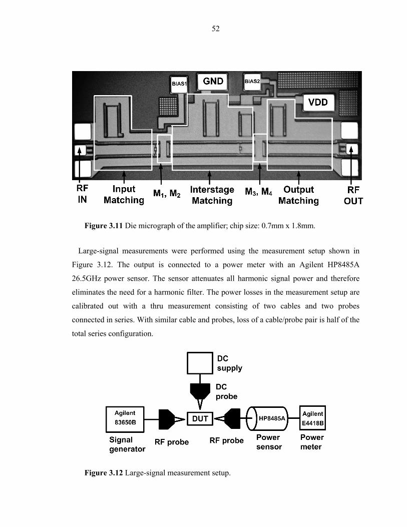
52
Figure 3.11 Die micrograph of the amplifier; chip size: 0.7mm x 1.8mm.
Large-signal measurements were performed using the measurement setup shown in
Figure 3.12. The output is connected to a power meter with an Agilent HP8485A
26.5GHz power sensor. The sensor attenuates all harmonic signal power and therefore
eliminates the need for a harmonic filter. The power losses in the measurement setup are
calibrated out with a thru measurement consisting of two cables and two probes
connected in series. With similar cable and probes, loss of a cable/probe pair is half of the
total series configuration.
Figure 3.12 Large-signal measurement setup.
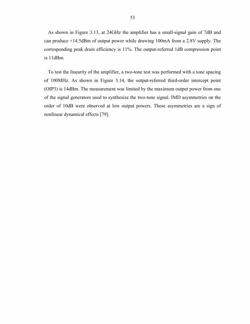
53
As shown in Figure 3.13, at 24GHz the amplifier has a small-signal gain of 7dB and
can produce +14.5dBm of output power while drawing 100mA from a 2.8V supply. The
corresponding peak drain efficiency is 11%. The output-referred 1dB compression point
is 11dBm.
To test the linearity of the amplifier, a two-tone test was performed with a tone spacing
of 100MHz. As shown in Figure 3.14, the output-referred third-order intercept point
(OIP3) is 14dBm. The measurement was limited by the maximum output power from one
of the signal generators used to synthesize the two-tone signal. IMD asymmetries on the
order of 10dB were observed at low output powers. These asymmetries are a sign of
nonlinear dynamical effects [79].
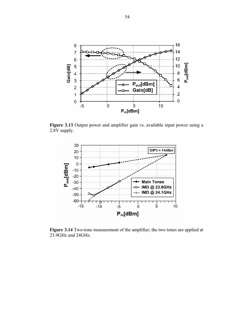
54
Figure 3.13 Output power and amplifier gain vs. available input power using a 2.8V supply.
Figure 3.14 Two-tone measurement of the amplifier; the two tones are applied at 23.9GHz and 24GHz.
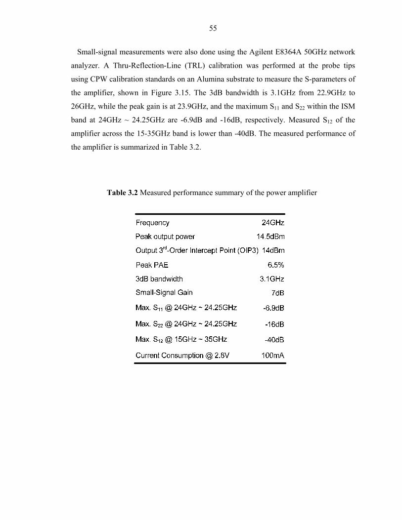
55
Small-signal measurements were also done using the Agilent E8364A 50GHz network
analyzer. A Thru-Reflection-Line (TRL) calibration was performed at the probe tips
using CPW calibration standards on an Alumina substrate to measure the S-parameters of
the amplifier, shown in Figure 3.15. The 3dB bandwidth is 3.1GHz from 22.9GHz to
26GHz, while the peak gain is at 23.9GHz, and the maximum S11 and S22 within the ISM
band at 24GHz ~ 24.25GHz are -6.9dB and -16dB, respectively. Measured S12 of the
amplifier across the 15-35GHz band is lower than -40dB. The measured performance of
the amplifier is summarized in Table 3.2.
Table 3.2 Measured performance summary of the power amplifier
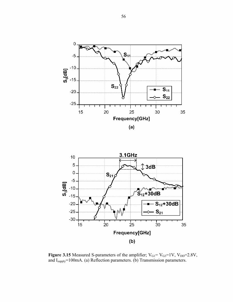
56
Figure 3.15 Measured S-parameters of the amplifier; VG1= VG3=1V, VDD=2.8V, and Isupply=100mA. (a) Reflection parameters. (b) Transmission parameters.
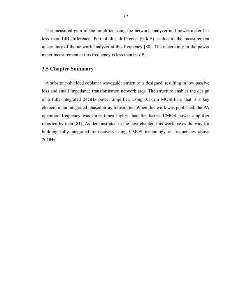
57
The measured gain of the amplifier using the network analyzer and power meter has
less than 1dB difference. Part of this difference (0.3dB) is due to the measurement
uncertainty of the network analyzer at this frequency [80]. The uncertainty in the power
meter measurement at this frequency is less than 0.1dB.
3.5 Chapter Summary
A substrate-shielded coplanar waveguide structure is designed, resulting in low passive
loss and small impedance transformation network area. The structure enables the design
of a fully-integrated 24GHz power amplifier, using 0.18μm MOSFETs, that is a key
element in an integrated phased-array transmitter. When this work was published, the PA
operation frequency was three times higher than the fastest CMOS power amplifier
reported by then [81]. As demonstrated in the next chapter, this work paves the way for
building fully-integrated transceivers using CMOS technology at frequencies above
20GHz.
58
Chapter 4 A Fully-Integrated 24GHz Phased-Array Transmitter in CMOS
A 4-Element Fully-Integrated 24GHz Phased-Array Transmitter in CMOS1
In this chapter the first fully-integrated 24GHz phased-array transmitter designed using
0.18µm CMOS transistors is presented. The four-element array includes four on-chip
CMOS power amplifiers, with outputs matched to 50Ω, that are each capable of
generating up to 14.5dBm output power at 24GHz. The heterodyne transmitter has two-
step quadrature upconversion architecture with LO frequencies of 4.8GHz and 19.2GHz,
which are generated by an on-chip frequency synthesizer. Four-bit LO-path phase
shifting is implemented in each element at 19.2GHz, and the transmitter achieves a peak-
to-null ratio of 23dB with raw beam-steering resolution of 7° for radiation normal to the
array. The transmitter can support data rates of 500Mbps on each channel (with QPSK
modulation) and occupies 6.8mm x 2.1mm of die area.
The project motivations and goals are briefly introduced in Section 4.1. The
architecture of the transmitter is detailed in Section 4.2. Section 4.3 describes the design
of the on-chip balun and power amplifier, followed by measurement results in Section 4.4.
Section 4.5 summarizes the chapter with conclusion.
4.1 Introduction
High frequency phased-array systems have been ubiquitous in the fields of radar and
radio astronomy [3]-[6]. However, these systems rely on specialized discrete components
and careful assembly of modules increasing cost and complexity of manufacturing.
Integration on silicon makes it possible to realize complex phased-array systems with on- 1 The 24GHz phased-array transmitter is a joint work of Abbas Komijani and Arun Natarajan. The phase selection circuitry and the upconversion chain were designed by Arun Natarajan and are discussed in [53].

59
chip mixed-signal and digital signal processing at lower cost and with higher reliability.
Furthermore, digital tuning and calibration in integrated systems can be used to improve
the performance of critical analog/RF parts [82][83]. Importantly, the very low
incremental cost of signal processing elements, i.e., transistors, and the benefits of
integration, such as short and robust interconnects and good component matching, enable
the realization of novel phased-array architectures that are designed specifically for
existing and emerging applications [84][85]. For instance, phased-array-based
transmitters and receivers, operating at high frequencies where large bandwidths are
available, are well-suited for high data rate directional point-to-point wireless
communication networks and for short-range radar applications such as collision
avoidance and assisted parking in automobiles.
The physical size of such integrated phased-array systems is restricted by the size of the
antennas and the spacing between them. In a system employing resonance-based antennas,
the antenna size and spacing decrease with an increase in frequency. Thus, the large
bandwidths and smaller physical system size render high frequencies attractive for
integrated phased-array implementation.
A particularly interesting frequency for integrated phased-array system implementation
is 24GHz. The Industrial, Scientific, and Medical (ISM) band at 24GHz has been opened
up for indoor wireless point-to-point communications by the FCC [35][36]. It permits
fixed, point-to-point wireless communication in the 24-24.25 GHz band subject to
limitations on the transmitted power and directionality of the transmitter.
In addition, 7GHz of spectrum from 22GHz to 29GHz has been allocated for
ultrawideband vehicular radar applications, making the 24GHz band appealing from both
wireless communication and car radar perspectives. Short-range vehicular radar systems
are expected to play an important role in collision prevention and driver assistance in the
future (e.g., assisted parking and blind spot detection). The 24 GHz band already has users,
particularly in the fields of remote sensing and astronomy. Interestingly, in addition to
specifications limiting transmitted power to different levels at different frequencies, i.e., the
spectral emissions mask, there is a spatial specification as well. The phased-array approach
60
provides a natural solution to these challenges.
CMOS process technologies are the most attractive among silicon-based technologies
for integrated-systems due to the benefits of scaling and the possibility of integrating the
digital backbone with the RF front-end. However, the low active gain of MOS transistors
and lossy passives at high frequencies have prevented any significant movement towards
integrating entire high-frequency phased-array systems on CMOS technologies. The
fully-integrated four-element 24GHz phased-array transmitter with on-chip power
amplifiers reported in this chapter is not only the first fully-integrated phased-array
transmitter but also the first system to demonstrate such levels of integration at 24GHz
using 0.18µm CMOS transistors. The transmitter reported in this work and the 8-element
phased-array SiGe receiver presented in [49] demonstrate the feasibility of 24GHz
phased-array systems in silicon-based processes.
4.2 Transmitter Architecture
The transmitter described in this work is based on the LO phase-shifting architecture
which was described in Section 2.6.2. Figure 4.1(a) shows a simplified four-element
phased-array transmitter with LO-path phase shifting. Relative phase shifts of
0, , 2 , and, 3φ φ φ are implemented in the elements. The angle of radiation, θ, is given by
1 .sin.RF
cd
φθω
− ⎛ ⎞= ⎜ ⎟
⎝ ⎠ (4.1)
where c is the velocity of light, and d is the spacing between the antennas. For d = λRF/2,
1sin φθπ
− ⎛ ⎞= ⎜ ⎟⎝ ⎠
. (4.2)
Figure 4.1(b) plots the array gain vs. angle of radiation for 16 uniformly spaced values
of φ with a step size of 22.5˚. As can be seen from the figure, the phase-shift resolution
is sufficient to radiate at all angles at close to peak array gain. The 3dB-beamwidth for
radiation that is normal to the axis of the array is 26˚, and the beam-steering resolution is
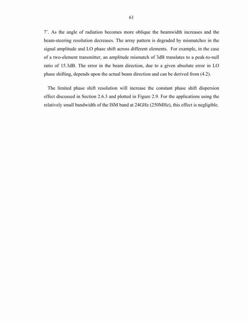
61
7˚. As the angle of radiation becomes more oblique the beamwidth increases and the
beam-steering resolution decreases. The array pattern is degraded by mismatches in the
signal amplitude and LO phase shift across different elements. For example, in the case
of a two-element transmitter, an amplitude mismatch of 3dB translates to a peak-to-null
ratio of 15.3dB. The error in the beam direction, due to a given absolute error in LO
phase shifting, depends upon the actual beam direction and can be derived from (4.2).
The limited phase shift resolution will increase the constant phase shift dispersion
effect discussed in Section 2.6.3 and plotted in Figure 2.9. For the applications using the
relatively small bandwidth of the ISM band at 24GHz (250MHz), this effect is negligible.
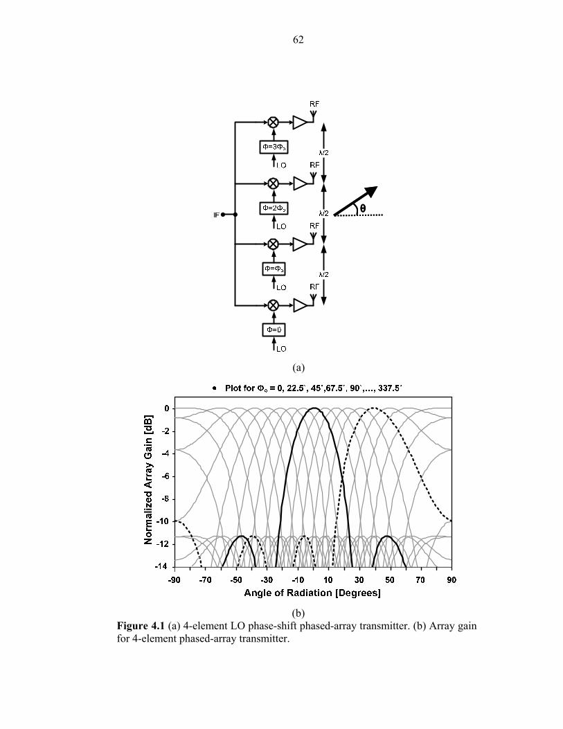
62
θθ
(a)
(b)
Figure 4.1 (a) 4-element LO phase-shift phased-array transmitter. (b) Array gain for 4-element phased-array transmitter.
63
Figure 4.2 shows the architecture and floorplan of the four-element transmitter [9]. The
four-element fully-integrated transmitter has on-chip power amplifiers [86] as well as an
integrated frequency synthesizer. Due to concerns related to frequency pulling, direct
upconversion was considered to be unsuitable. As shown in Figure 4.3, a two-step
upconversion architecture was chosen for the transmitter with LO frequencies of 4.8GHz
and 19.2GHz. The two LO frequencies are generated by a single synthesizer loop using a
divide-by-four.
Quadrature upconversion was implemented in both stages [87]. The image attenuation
of the first upconversion step depends upon the matching and quadrature accuracy of the
first upconversion step. The image signal of the second upconversion step falls at
14.4GHz and is therefore attenuated not only by the quadrature architecture but also by
the tuned stages at RF.
In the signal path, the baseband I and Q signals are upconverted to 4.8GHz by a pair of
quadrature upconversion mixers. The 4.8GHz I and Q signals are buffered and provided
to the 4.8GHz-to-24GHz upconversion mixers in each element. The output of the mixers
is amplified, and differential to single-ended conversion is performed to drive the on-chip
single-ended CMOS power amplifiers, which are matched at the output to 50Ω.
In the LO path, the output of the 16-phase 19.2GHz VCO is provided to the phase-
selectors in each element. These phase-selectors select the right phase of the LO in each
element for the desired beam direction. The phase-selection circuitry is controlled by
shift-registers that can be programmed using a digital serial interface, enabling electronic
beam-steering. The VCO is part of an on-chip frequency synthesizer which generates the
19.2GHz LO signals from a 75MHz reference. A divide-by-four in the synthesizer loop
generates the 4.8GHz LO I and Q signals for the first upconversion step.
64
Figure 4.2 Architecture and floorplan of 24GHz 4-element phased-array transmitter.
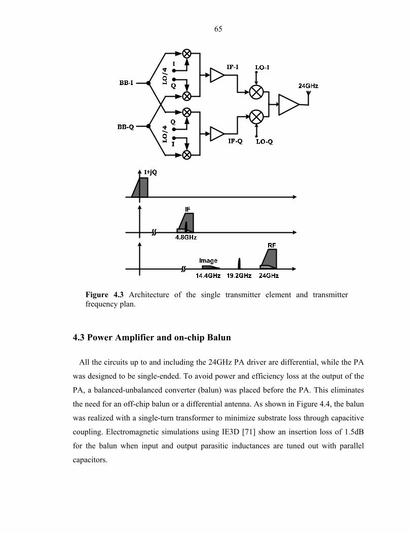
65
4.3 Power Amplifier and on-chip Balun
All the circuits up to and including the 24GHz PA driver are differential, while the PA
was designed to be single-ended. To avoid power and efficiency loss at the output of the
PA, a balanced-unbalanced converter (balun) was placed before the PA. This eliminates
the need for an off-chip balun or a differential antenna. As shown in Figure 4.4, the balun
was realized with a single-turn transformer to minimize substrate loss through capacitive
coupling. Electromagnetic simulations using IE3D [71] show an insertion loss of 1.5dB
for the balun when input and output parasitic inductances are tuned out with parallel
capacitors.
Figure 4.3 Architecture of the single transmitter element and transmitter frequency plan.
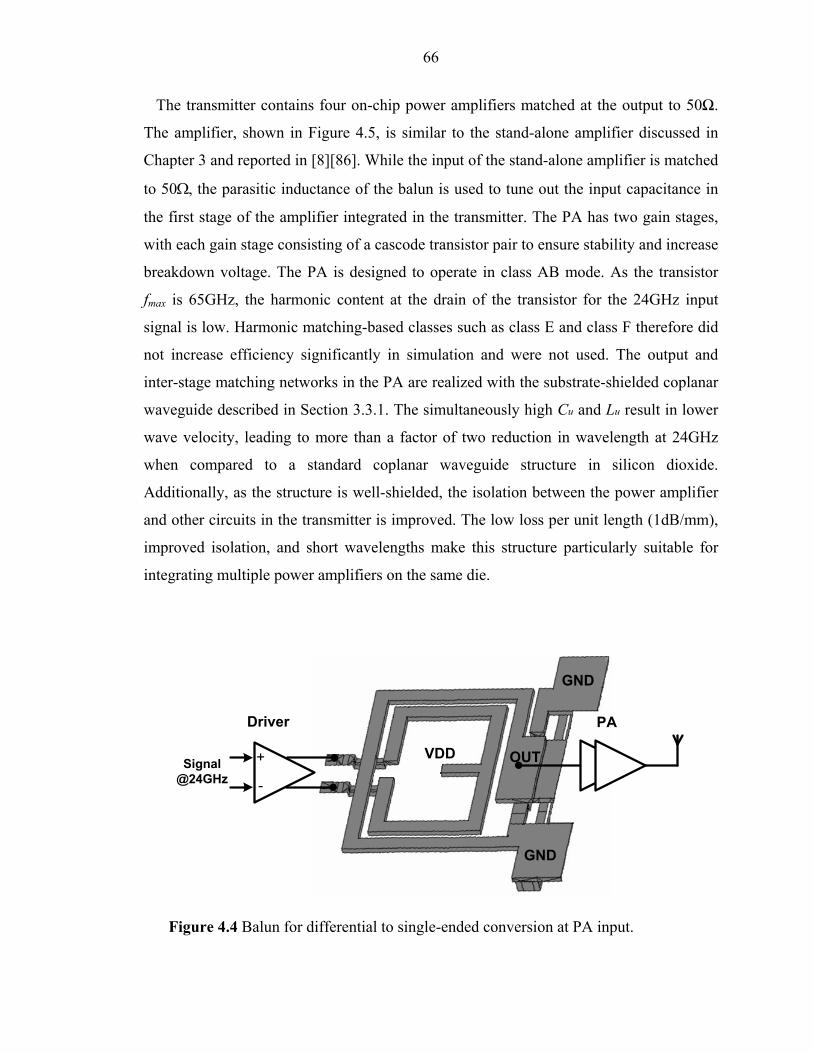
66
The transmitter contains four on-chip power amplifiers matched at the output to 50Ω.
The amplifier, shown in Figure 4.5, is similar to the stand-alone amplifier discussed in
Chapter 3 and reported in [8][86]. While the input of the stand-alone amplifier is matched
to 50Ω, the parasitic inductance of the balun is used to tune out the input capacitance in
the first stage of the amplifier integrated in the transmitter. The PA has two gain stages,
with each gain stage consisting of a cascode transistor pair to ensure stability and increase
breakdown voltage. The PA is designed to operate in class AB mode. As the transistor
fmax is 65GHz, the harmonic content at the drain of the transistor for the 24GHz input
signal is low. Harmonic matching-based classes such as class E and class F therefore did
not increase efficiency significantly in simulation and were not used. The output and
inter-stage matching networks in the PA are realized with the substrate-shielded coplanar
waveguide described in Section 3.3.1. The simultaneously high Cu and Lu result in lower
wave velocity, leading to more than a factor of two reduction in wavelength at 24GHz
when compared to a standard coplanar waveguide structure in silicon dioxide.
Additionally, as the structure is well-shielded, the isolation between the power amplifier
and other circuits in the transmitter is improved. The low loss per unit length (1dB/mm),
improved isolation, and short wavelengths make this structure particularly suitable for
integrating multiple power amplifiers on the same die.
PA
OUT
GND
GND
VDD+
-Signal
@24GHz
Driver
Figure 4.4 Balun for differential to single-ended conversion at PA input.
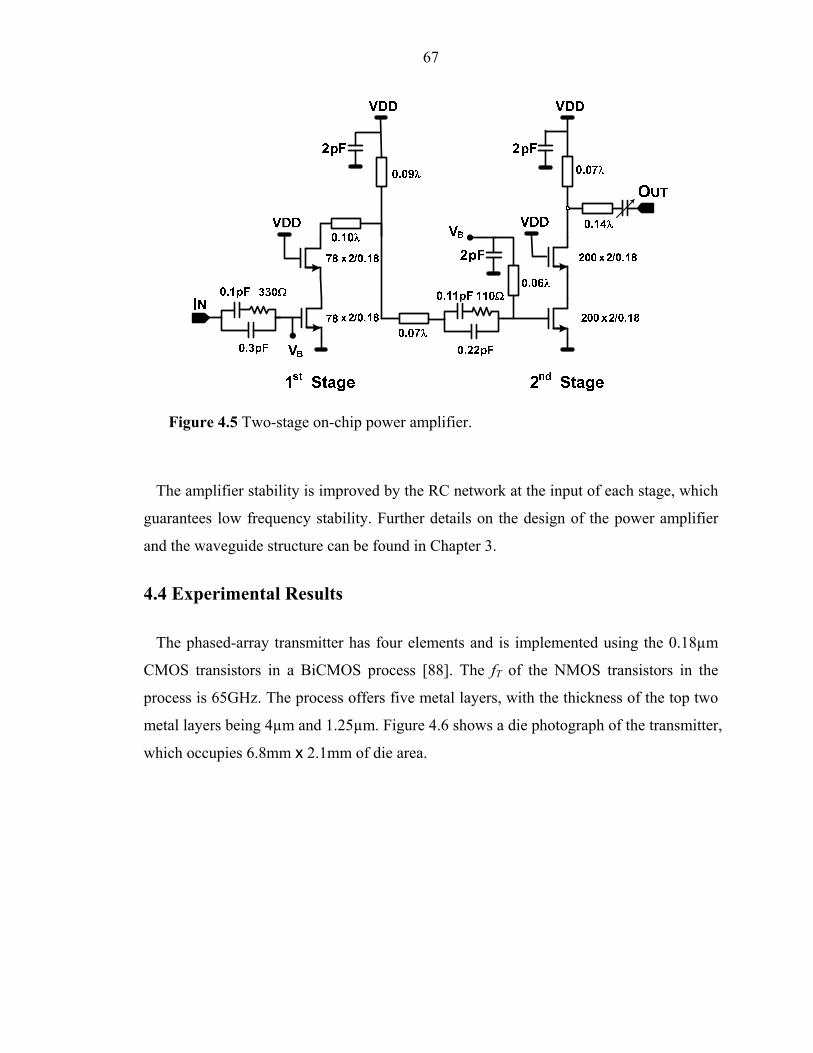
67
The amplifier stability is improved by the RC network at the input of each stage, which
guarantees low frequency stability. Further details on the design of the power amplifier
and the waveguide structure can be found in Chapter 3.
4.4 Experimental Results
The phased-array transmitter has four elements and is implemented using the 0.18µm
CMOS transistors in a BiCMOS process [88]. The fT of the NMOS transistors in the
process is 65GHz. The process offers five metal layers, with the thickness of the top two
metal layers being 4µm and 1.25µm. Figure 4.6 shows a die photograph of the transmitter,
which occupies 6.8mm x 2.1mm of die area.
Figure 4.5 Two-stage on-chip power amplifier.
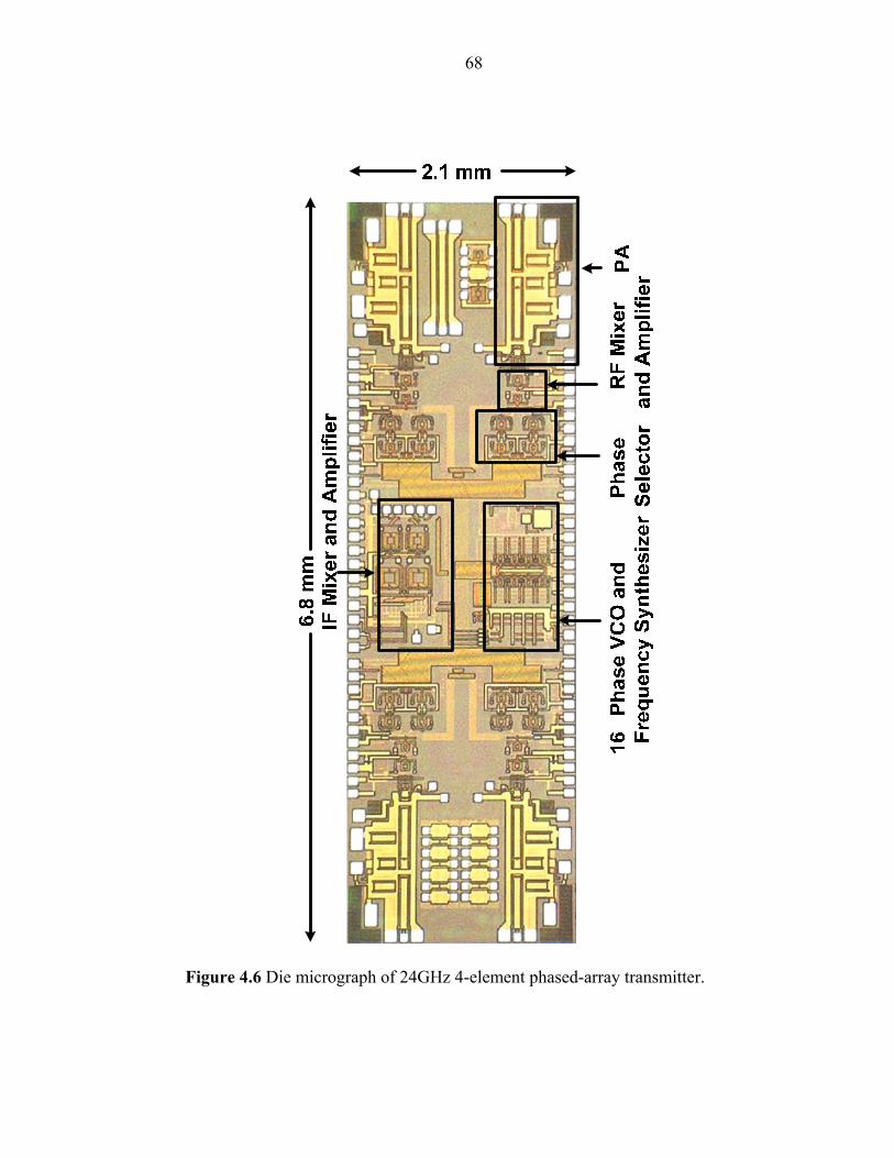
68
Figure 4.6 Die micrograph of 24GHz 4-element phased-array transmitter.
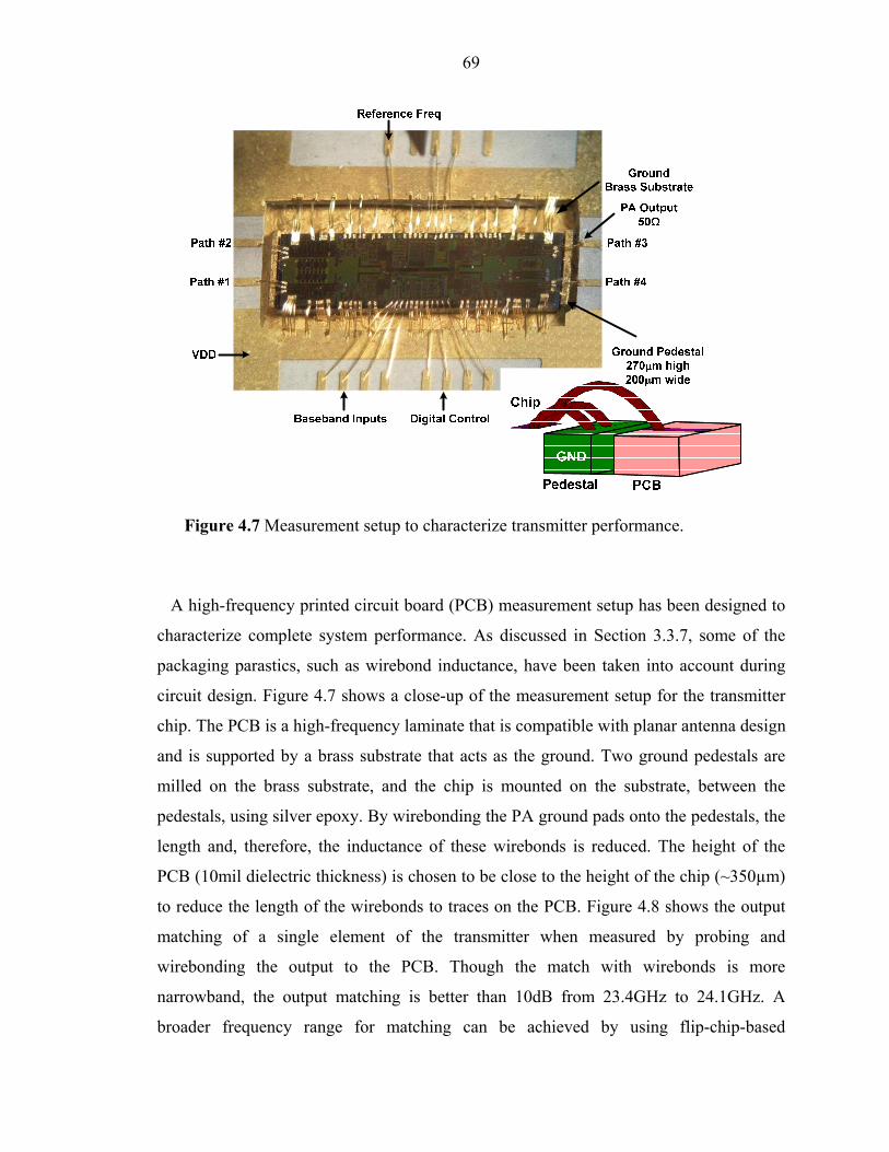
69
A high-frequency printed circuit board (PCB) measurement setup has been designed to
characterize complete system performance. As discussed in Section 3.3.7, some of the
packaging parastics, such as wirebond inductance, have been taken into account during
circuit design. Figure 4.7 shows a close-up of the measurement setup for the transmitter
chip. The PCB is a high-frequency laminate that is compatible with planar antenna design
and is supported by a brass substrate that acts as the ground. Two ground pedestals are
milled on the brass substrate, and the chip is mounted on the substrate, between the
pedestals, using silver epoxy. By wirebonding the PA ground pads onto the pedestals, the
length and, therefore, the inductance of these wirebonds is reduced. The height of the
PCB (10mil dielectric thickness) is chosen to be close to the height of the chip (~350µm)
to reduce the length of the wirebonds to traces on the PCB. Figure 4.8 shows the output
matching of a single element of the transmitter when measured by probing and
wirebonding the output to the PCB. Though the match with wirebonds is more
narrowband, the output matching is better than 10dB from 23.4GHz to 24.1GHz. A
broader frequency range for matching can be achieved by using flip-chip-based
Figure 4.7 Measurement setup to characterize transmitter performance.
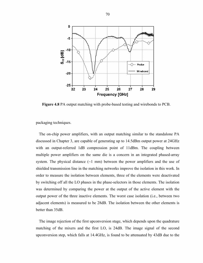
70
packaging techniques.
The on-chip power amplifiers, with an output matching similar to the standalone PA
discussed in Chapter 3, are capable of generating up to 14.5dBm output power at 24GHz
with an output-referred 1dB compression point of 11dBm. The coupling between
multiple power amplifiers on the same die is a concern in an integrated phased-array
system. The physical distance (~1 mm) between the power amplifiers and the use of
shielded transmission line in the matching networks improve the isolation in this work. In
order to measure the isolation between elements, three of the elements were deactivated
by switching off all the LO phases in the phase-selectors in those elements. The isolation
was determined by comparing the power at the output of the active element with the
output power of the three inactive elements. The worst case isolation (i.e., between two
adjacent elements) is measured to be 28dB. The isolation between the other elements is
better than 35dB.
The image rejection of the first upconversion stage, which depends upon the quadrature
matching of the mixers and the first LO, is 24dB. The image signal of the second
upconversion step, which falls at 14.4GHz, is found to be attenuated by 43dB due to the
Figure 4.8 PA output matching with probe-based testing and wirebonds to PCB.
71
additional attenuation provided by the tuned stages at RF. The limited bandwidth of the
antenna will further reduce the image of the second upconversion.
To measure the performance of the transmitter alone, without antenna non-idealities
such as coupling, the different propagation delays for each element for each direction of
radiation have to be replicated. This is done by connecting the output of each element to
variable phase shifters (Figure 4.9). By varying the relative phase shift in the external
phase shifters, the propagation delays for each beam direction can be emulated. The
output of the phase shifters is combined and measured using a spectrum analyzer or a
power meter. Figure 4.10 shows the measured performance of the transmitter with two
elements active and with all four elements active. When compared to theory, these results
demonstrate the proper functioning of the phased-array transmitter. The worst-case peak-
to-null ratio with all four elements active is 23dB.
While the PA has a bandwidth of 3.1GHz, the bandwidth of the entire transmitter is
constrained by the bandwidth of the IF stages and also by the cascade of tuned stages at
IF and RF. Figure 4.11, which shows the measured spectrum of the transmitter when a
100Mbps and 500Mbps QPSK signal is provided at baseband, indicates that the
transmitter is capable of supporting high data rates.
The entire system with four on-chip power amplifiers draws 788mA from a 2.5V
supply. The measured performance of the chip is summarized in Table 4.1.
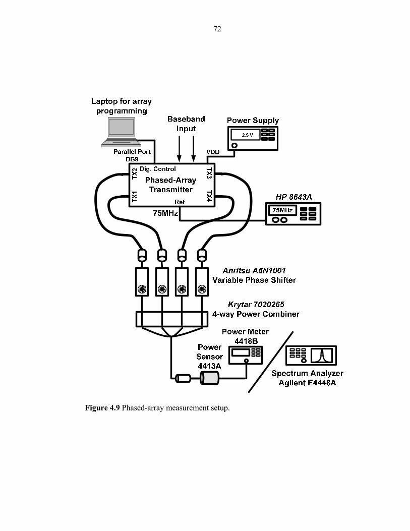
72
Figure 4.9 Phased-array measurement setup.
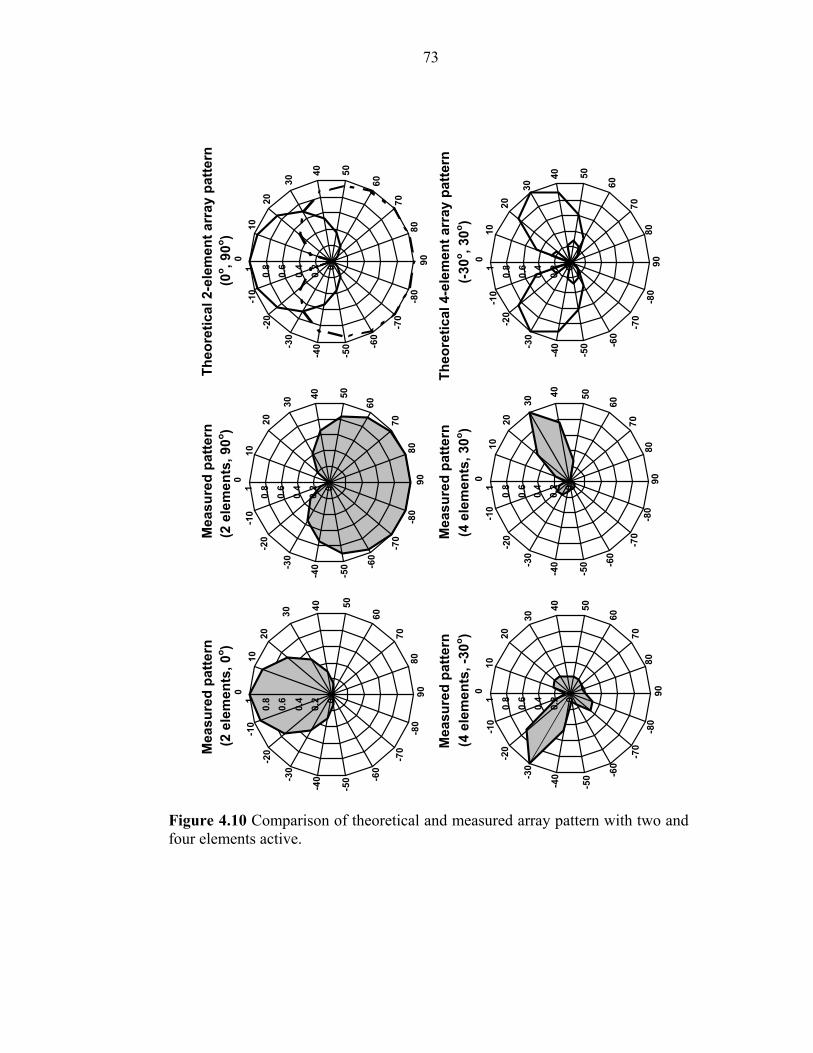
73
Figure 4.10 Comparison of theoretical and measured array pattern with two and four elements active.
Theo
retic
al 2
-ele
men
t arr
ay p
atte
rnM
easu
red
patte
rnM
easu
red
patte
rn
Theo
retic
al 4
-ele
men
t arr
ay p
atte
rnM
easu
red
patte
rnM
easu
red
patte
rn
00.
20.
4
0.6
0.81
010
20
30
40 50
60
7080
90-8
0-7
0
-60
-50
-40-3
0
-20
-10
00.
20.
40.
60.
810
1020
30
40 50
60
7080
90-8
0-7
0
-60
-50
-40-3
0
-20
-10
00.
20.
40.
60.
810
1020
30
40 50
60
7080
90-8
0-7
0
-60
-50
-40-3
0
-20
-10
00.
20.
40.
60.
810
1020
30
40 50
60
7080
90-8
0-7
0
-60
-50
-40-3
0
-20
-10
(2 e
lem
ents
, 0o )
(2 e
lem
ents
, 90o )
(0o , 9
0o )
(4 e
lem
ents
, -30
o )(4
ele
men
ts, 3
0o )(-3
0o , 30o )
00.
20.
4
0.6
0.81
010
20
30 40 50
60
7080
90-8
0-7
0
-60
-50
-40-3
0
-20
-10
00.
20.
40.
60.
810
10
20
30
40 50
60
7080
90-8
0-7
0
-60
-50
-40-3
0
-20
-10
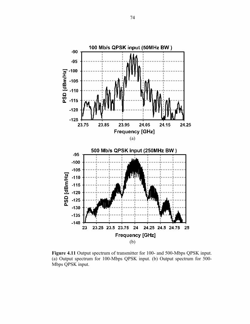
74
(a)
PSD
[dB
m/H
z]
(b)
Figure 4.11 Output spectrum of transmitter for 100- and 500-Mbps QPSK input. (a) Output spectrum for 100-Mbps QPSK input. (b) Output spectrum for 500-Mbps QPSK input.
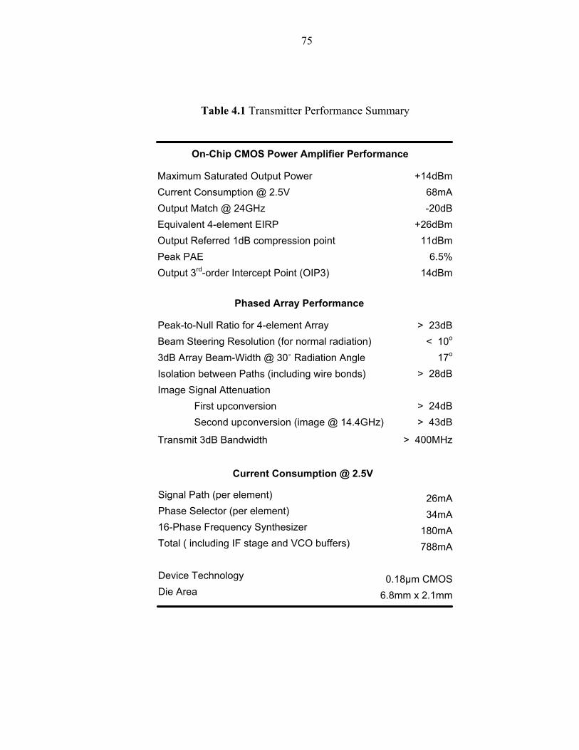
75
Table 4.1 Transmitter Performance Summary
On-Chip CMOS Power Amplifier Performance
Maximum Saturated Output PowerCurrent Consumption @ 2.5VOutput Match @ 24GHzEquivalent 4-element EIRPOutput Referred 1dB compression pointPeak PAEOutput 3rd-order Intercept Point (OIP3)
Phased Array Performance
Peak-to-Null Ratio for 4-element ArrayBeam Steering Resolution (for normal radiation)3dB Array Beam-Width @ 30˚ Radiation Angle Isolation between Paths (including wire bonds)Image Signal Attenuation First upconversion Second upconversion (image @ 14.4GHz)
Transmit 3dB Bandwidth
Current Consumption @ 2.5V
Signal Path (per element)Phase Selector (per element)16-Phase Frequency SynthesizerTotal ( including IF stage and VCO buffers)
Device TechnologyDie Area
+14dBm68mA-20dB
+26dBm11dBm
6.5%14dBm
> 23dB< 10o
17o
> 28dB
> 24dB > 43dB
> 400MHz
26mA34mA
180mA788mA
0.18μm CMOS6.8mm x 2.1mm
76
4.5 Chapter Summary
In this chapter, the first fully-integrated phased-array transmitter has been demonstrated
using 0.18µm CMOS transistors, proving the feasibility of high frequency integrated
phased-array systems on silicon-based processes. The four-bit LO-path phase-shifting
approach adopted in the transmitter has better than 10° beam-steering resolution for
radiation normal to the array. Each on-chip PA is capable of generating up to 14.5dBm
output power, translating to an EIRP of 26.5dBm. The transmitter is capable of
supporting data rates in excess of 500Mbps and is well-suited for 24GHz wireless links.
The fully-integrated four-element 24GHz phased-array transmitter with on-chip power
amplifiers reported in this chapter is not only the first fully-integrated phased-array
transmitter but also the first system to demonstrate such levels of integration at 24GHz
using 0.18µm CMOS transistors. This work demonstrates that CMOS technology is a
viable candidate for building fully-integrated transmitters at frequencies higher than
20GHz.
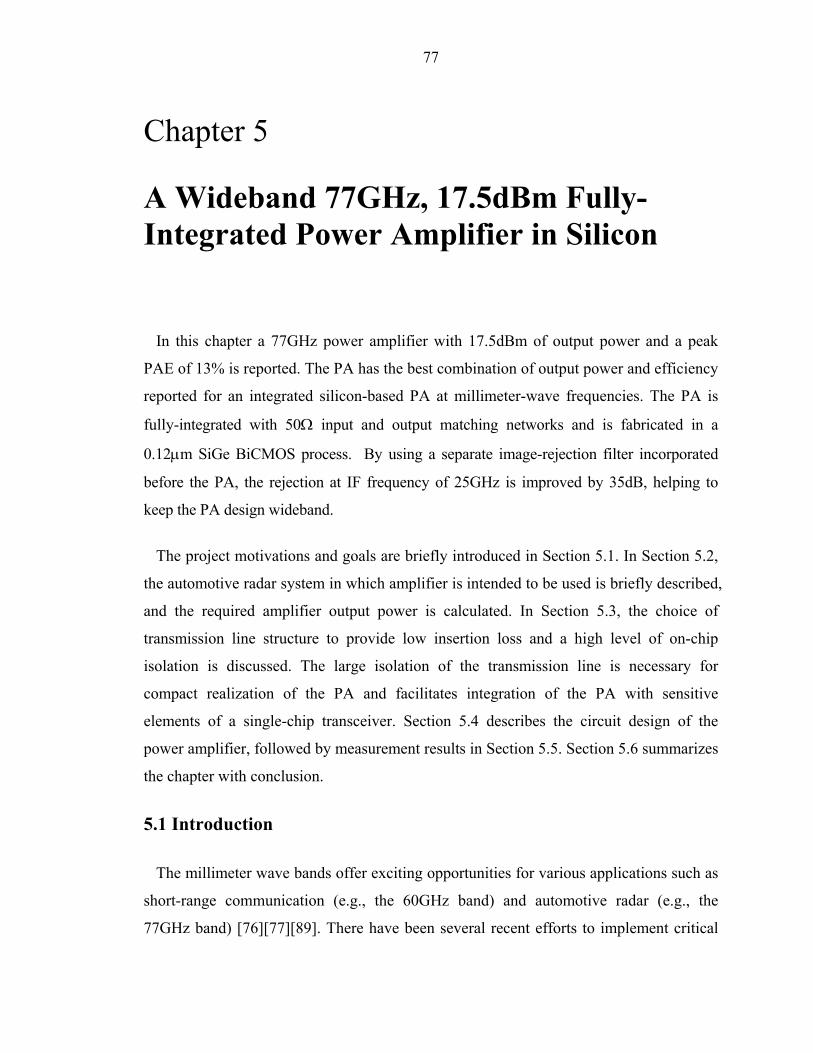
77
Chapter 5 A Wideband 77GHz, 17.5dBm Fully-Integrated Power Amplifier in Silicon
A Wideband 77GHz, 17.5dBm Fully-Integrated Power Amplifier in Silicon
In this chapter a 77GHz power amplifier with 17.5dBm of output power and a peak
PAE of 13% is reported. The PA has the best combination of output power and efficiency
reported for an integrated silicon-based PA at millimeter-wave frequencies. The PA is
fully-integrated with 50Ω input and output matching networks and is fabricated in a
0.12μm SiGe BiCMOS process. By using a separate image-rejection filter incorporated
before the PA, the rejection at IF frequency of 25GHz is improved by 35dB, helping to
keep the PA design wideband.
The project motivations and goals are briefly introduced in Section 5.1. In Section 5.2,
the automotive radar system in which amplifier is intended to be used is briefly described,
and the required amplifier output power is calculated. In Section 5.3, the choice of
transmission line structure to provide low insertion loss and a high level of on-chip
isolation is discussed. The large isolation of the transmission line is necessary for
compact realization of the PA and facilitates integration of the PA with sensitive
elements of a single-chip transceiver. Section 5.4 describes the circuit design of the
power amplifier, followed by measurement results in Section 5.5. Section 5.6 summarizes
the chapter with conclusion.
5.1 Introduction
The millimeter wave bands offer exciting opportunities for various applications such as
short-range communication (e.g., the 60GHz band) and automotive radar (e.g., the
77GHz band) [76][77][89]. There have been several recent efforts to implement critical
78
mm-wave blocks such as LNAs, VCOs, and PAs in silicon [64][76][77][90]. Penetration
of silicon integrated circuits to these frequency bands can bring the unchallenged reign of
compound semiconductors at these frequencies to an end. Although the performance of
silicon-based implementations needs to improve to match those offered by III-V-based
technologies, the true strength of silicon is in its unmatched level of integration, which
will enable a new level of complexity encompassing microwave, analog, and digital
blocks [1][9][11][12]. This unprecedented integration will result in new system-level
architectures at these frequencies previously impractical using lower yield compound
semiconductor processes, resulting in globally optimum solutions in terms of cost and
performance.
Perhaps the most challenging building block at mm-wave frequencies is the power
amplifier (PA). Prior works in silicon involve a 77GHz SiGe amplifier with 15.5dBm
output power and 5% power added efficiency (PAE) [90]. Also, in [76] and [77] two
SiGe PAs at 77GHz and 60GHz with 10-13dBm output power and 3-4% PAE have been
reported. In [91], by using multiple parallel transistors, power level has been increased to
21dBm, but still the PAE has been limited to 3%. Although further improvements in
output power using power combining is possible, the main challenge for the silicon
implementation so far has been improving the PAE. As a comparison point at similar
frequencies, PAs using III-V technologies deliver 23-28dBm of output power with 20%-
40% of PAE [92]-[95].
5.2 The Required Amplifier Power for Automotive RADAR Application
In long-range radar for cruise control and collision avoidance, the need to detect far
away cars and discriminate between closely spaced vehicles demands small radiation
beamwidth and fine beam steering resolution. As shown in Figure 5.1, the required
azimuthal resolution for the long-range radar should be around 3o. To avoid reflections
from entrance of tunnels and bridges, the required beam width in the H-plane (elevation)
should also be less than 3o. The corresponding system directivity, as shown in Figure 5.1,
will be 36dBi. Normally, for the car radar applications, the beam steering is achieved
using a dielectric lens or a Rotman lens [96]-[98]. Instead, in the radar system that the
79
amplifier in this work is designed for, a phased-array transceiver with beam steering in
both TX and RX paths is employed. This system will be presented in Chapter 6. In this
case the directivity requirement of each path is relaxed, hence reducing the required array
aperture. The 18dB required directivity at each path can be achieved with 16 elements
providing 12dB of array directivity combined with a typical directivity of a patch or
dipole antenna (~5dB). Since there is no need to scan in the elevation plane, the required
directivity in the elevation can be realized by narrowing the antenna beam in the
elevation plane (e.g., using serially-fed patches [98]-[100]). In this case just four elements
for beam steering in azimuthal plane will be enough.
Assuming 18dB of directivity for transmit and receive paths and 3dB of insertion loss
for the antenna, if each power amplifier in the 4-element phased-array generates 15dBm
of output power, the received signal power calculated using standard radar equation will
be -116dBm [74]. In this case, the target is assumed to have a cross section of 1m2
located 100m from the transmitter. Using a 4-element phased-array system with 6dB
signal to noise ratio (SNR) improvement and a receiver noise figure of 8dB [12], the
radar SNR for a 300MHz bandwidth will be -11dB. By using multiple scans or pseudo-
noise (PN) modulation similar to [40] the radar sensitivity can be improved.
By employing a commonly-used FM-CW or pulse-Doppler technique, the transmitter
power amplifier will experience a constant-envelope signal, relaxing its linearity
requirements.
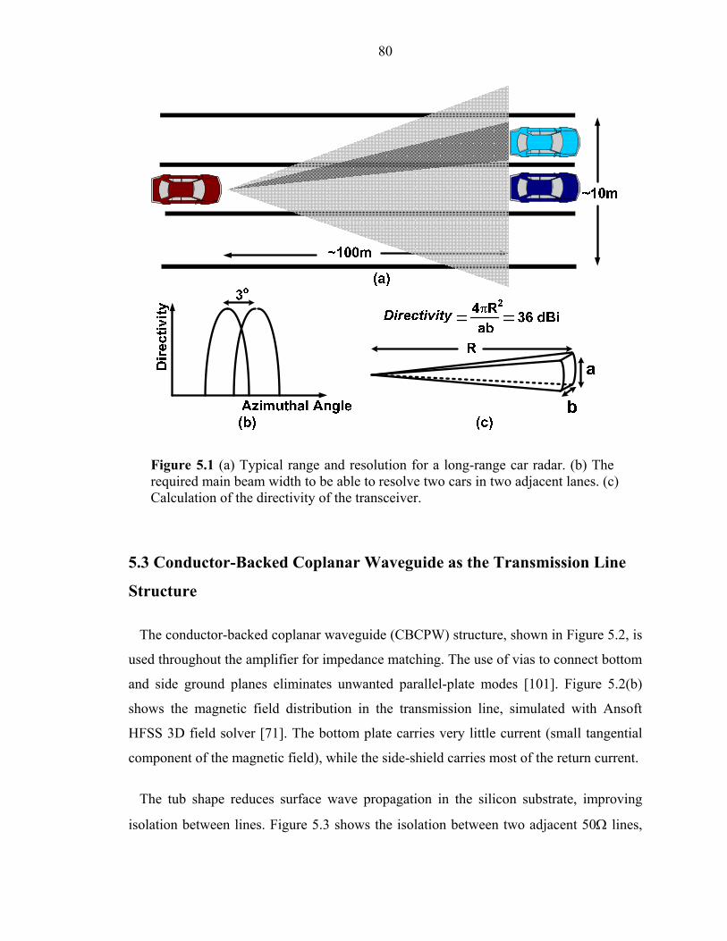
80
5.3 Conductor-Backed Coplanar Waveguide as the Transmission Line
Structure
The conductor-backed coplanar waveguide (CBCPW) structure, shown in Figure 5.2, is
used throughout the amplifier for impedance matching. The use of vias to connect bottom
and side ground planes eliminates unwanted parallel-plate modes [101]. Figure 5.2(b)
shows the magnetic field distribution in the transmission line, simulated with Ansoft
HFSS 3D field solver [71]. The bottom plate carries very little current (small tangential
component of the magnetic field), while the side-shield carries most of the return current.
The tub shape reduces surface wave propagation in the silicon substrate, improving
isolation between lines. Figure 5.3 shows the isolation between two adjacent 50Ω lines,
Figure 5.1 (a) Typical range and resolution for a long-range car radar. (b) The required main beam width to be able to resolve two cars in two adjacent lanes. (c) Calculation of the directivity of the transceiver.
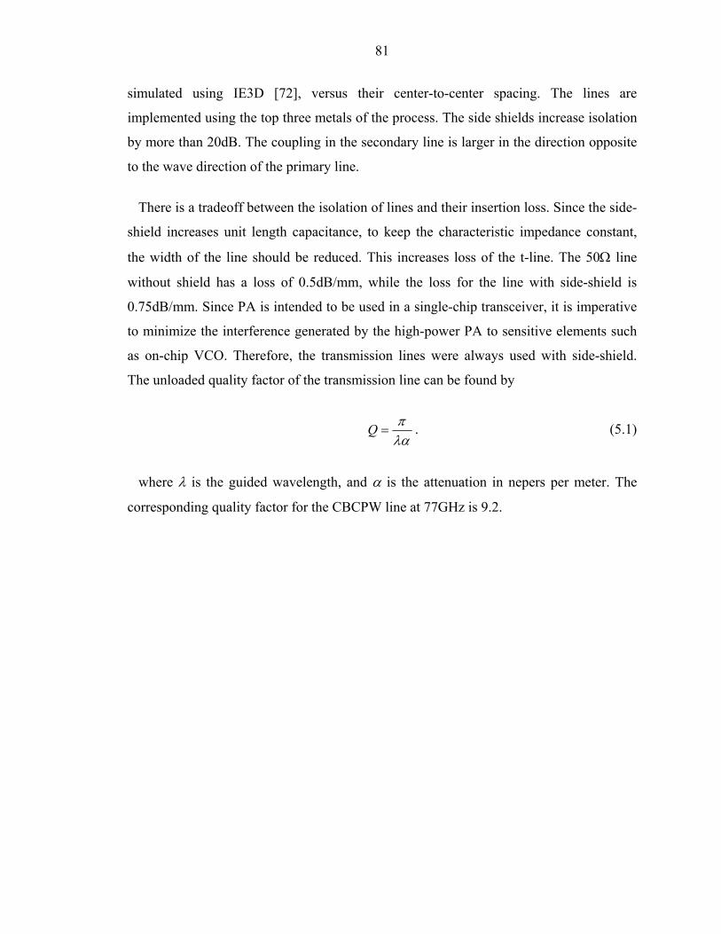
81
simulated using IE3D [72], versus their center-to-center spacing. The lines are
implemented using the top three metals of the process. The side shields increase isolation
by more than 20dB. The coupling in the secondary line is larger in the direction opposite
to the wave direction of the primary line.
There is a tradeoff between the isolation of lines and their insertion loss. Since the side-
shield increases unit length capacitance, to keep the characteristic impedance constant,
the width of the line should be reduced. This increases loss of the t-line. The 50Ω line
without shield has a loss of 0.5dB/mm, while the loss for the line with side-shield is
0.75dB/mm. Since PA is intended to be used in a single-chip transceiver, it is imperative
to minimize the interference generated by the high-power PA to sensitive elements such
as on-chip VCO. Therefore, the transmission lines were always used with side-shield.
The unloaded quality factor of the transmission line can be found by
λαπ
=Q . (5.1)
where λ is the guided wavelength, and α is the attenuation in nepers per meter. The
corresponding quality factor for the CBCPW line at 77GHz is 9.2.
82
(a)
(b)
Figure 5.2 (a) Conductor-backed coplanar waveguide transmission line structure used for matching in the amplifier. (b) The simulated magnetic field distribution of the structure, showing most of the return current coming from the side shields.

83
(a)
(b)
Figure 5.3 The simulated isolation between two side-by-side 400μm, 50Ω microstrip lines with sideshield (W = 5μm, S = 7.5μm) and without sideshield (W = 13μm).
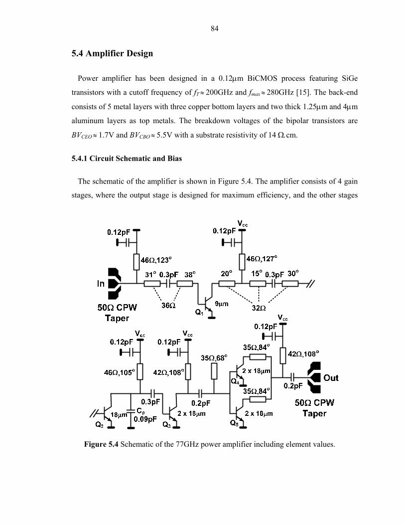
84
5.4 Amplifier Design
Power amplifier has been designed in a 0.12μm BiCMOS process featuring SiGe
transistors with a cutoff frequency of fT ≈ 200GHz and fmax ≈ 280GHz [15]. The back-end
consists of 5 metal layers with three copper bottom layers and two thick 1.25μm and 4μm
aluminum layers as top metals. The breakdown voltages of the bipolar transistors are
BVCEO ≈ 1.7V and BVCBO ≈ 5.5V with a substrate resistivity of 14 Ω.cm.
5.4.1 Circuit Schematic and Bias
The schematic of the amplifier is shown in Figure 5.4. The amplifier consists of 4 gain
stages, where the output stage is designed for maximum efficiency, and the other stages
Figure 5.4 Schematic of the 77GHz power amplifier including element values.
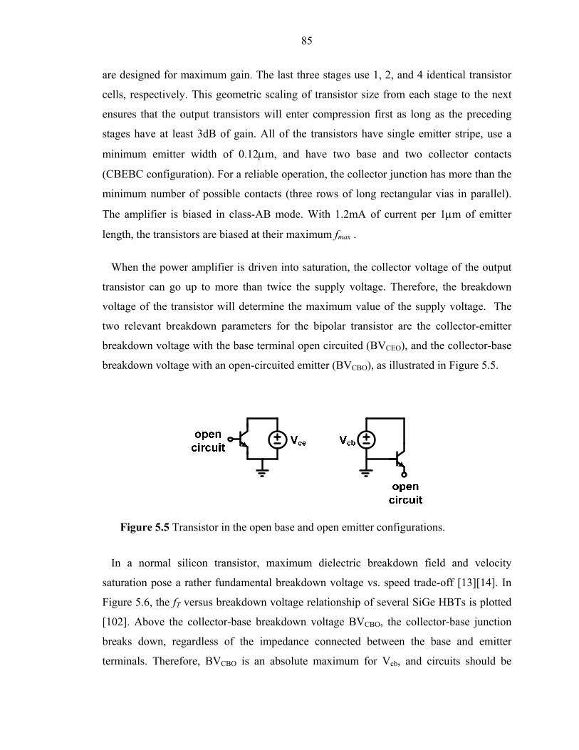
85
are designed for maximum gain. The last three stages use 1, 2, and 4 identical transistor
cells, respectively. This geometric scaling of transistor size from each stage to the next
ensures that the output transistors will enter compression first as long as the preceding
stages have at least 3dB of gain. All of the transistors have single emitter stripe, use a
minimum emitter width of 0.12μm, and have two base and two collector contacts
(CBEBC configuration). For a reliable operation, the collector junction has more than the
minimum number of possible contacts (three rows of long rectangular vias in parallel).
The amplifier is biased in class-AB mode. With 1.2mA of current per 1μm of emitter
length, the transistors are biased at their maximum fmax .
When the power amplifier is driven into saturation, the collector voltage of the output
transistor can go up to more than twice the supply voltage. Therefore, the breakdown
voltage of the transistor will determine the maximum value of the supply voltage. The
two relevant breakdown parameters for the bipolar transistor are the collector-emitter
breakdown voltage with the base terminal open circuited (BVCEO), and the collector-base
breakdown voltage with an open-circuited emitter (BVCBO), as illustrated in Figure 5.5.
Figure 5.5 Transistor in the open base and open emitter configurations.
In a normal silicon transistor, maximum dielectric breakdown field and velocity
saturation pose a rather fundamental breakdown voltage vs. speed trade-off [13][14]. In
Figure 5.6, the fT versus breakdown voltage relationship of several SiGe HBTs is plotted
[102]. Above the collector-base breakdown voltage BVCBO, the collector-base junction
breaks down, regardless of the impedance connected between the base and emitter
terminals. Therefore, BVCBO is an absolute maximum for Vcb, and circuits should be
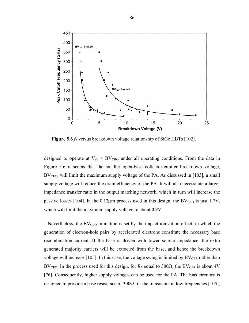
86
designed to operate at Vcb < BVCBO under all operating conditions. From the data in
Figure 5.6 it seems that the smaller open-base collector-emitter breakdown voltage,
BVCEO, will limit the maximum supply voltage of the PA. As discussed in [103], a small
supply voltage will reduce the drain efficiency of the PA. It will also necessitate a larger
impedance transfer ratio in the output matching network, which in turn will increase the
passive losses [104]. In the 0.12μm process used in this design, the BVCEO is just 1.7V,
which will limit the maximum supply voltage to about 0.9V.
Nevertheless, the BVCEO limitation is set by the impact ionization effect, in which the
generation of electron-hole pairs by accelerated electrons constitute the necessary base
recombination current. If the base is driven with lower source impedance, the extra
generated majority carriers will be extracted from the base, and hence the breakdown
voltage will increase [105]. In this case, the voltage swing is limited by BVCER rather than
BVCEO. In the process used for this design, for RB equal to 300Ω, the BVCER is about 4V
[76]. Consequently, higher supply voltages can be used for the PA. The bias circuitry is
designed to provide a base resistance of 300Ω for the transistors in low frequencies [105],
Figure 5.6 fT versus breakdown voltage relationship of SiGe HBTs [102].
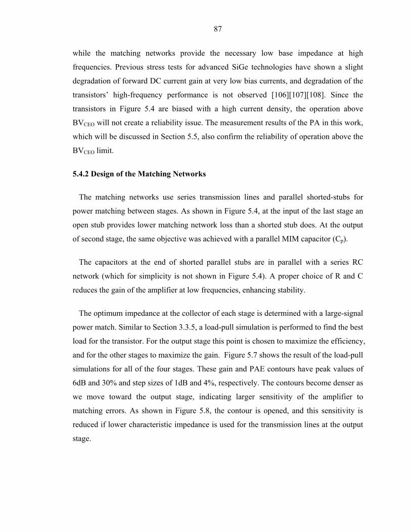
87
while the matching networks provide the necessary low base impedance at high
frequencies. Previous stress tests for advanced SiGe technologies have shown a slight
degradation of forward DC current gain at very low bias currents, and degradation of the
transistors’ high-frequency performance is not observed [106][107][108]. Since the
transistors in Figure 5.4 are biased with a high current density, the operation above
BVCEO will not create a reliability issue. The measurement results of the PA in this work,
which will be discussed in Section 5.5, also confirm the reliability of operation above the
BVCEO limit.
5.4.2 Design of the Matching Networks
The matching networks use series transmission lines and parallel shorted-stubs for
power matching between stages. As shown in Figure 5.4, at the input of the last stage an
open stub provides lower matching network loss than a shorted stub does. At the output
of second stage, the same objective was achieved with a parallel MIM capacitor (Cp).
The capacitors at the end of shorted parallel stubs are in parallel with a series RC
network (which for simplicity is not shown in Figure 5.4). A proper choice of R and C
reduces the gain of the amplifier at low frequencies, enhancing stability.
The optimum impedance at the collector of each stage is determined with a large-signal
power match. Similar to Section 3.3.5, a load-pull simulation is performed to find the best
load for the transistor. For the output stage this point is chosen to maximize the efficiency,
and for the other stages to maximize the gain. Figure 5.7 shows the result of the load-pull
simulations for all of the four stages. These gain and PAE contours have peak values of
6dB and 30% and step sizes of 1dB and 4%, respectively. The contours become denser as
we move toward the output stage, indicating larger sensitivity of the amplifier to
matching errors. As shown in Figure 5.8, the contour is opened, and this sensitivity is
reduced if lower characteristic impedance is used for the transmission lines at the output
stage.
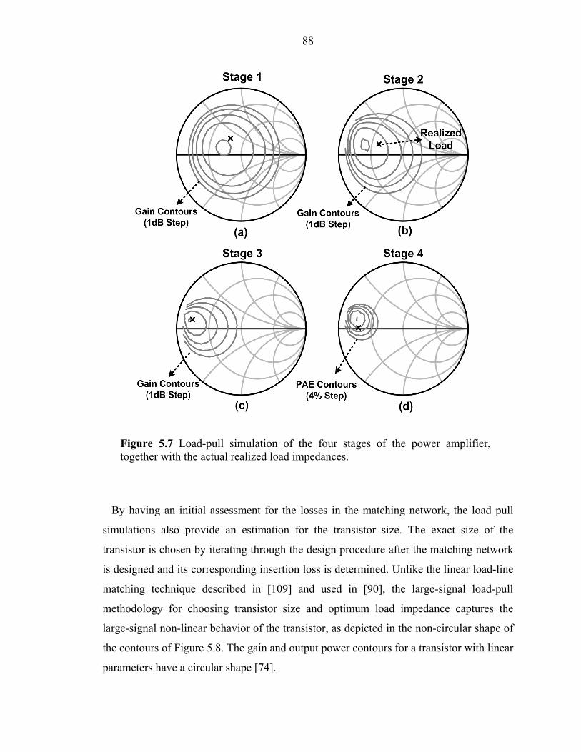
88
By having an initial assessment for the losses in the matching network, the load pull
simulations also provide an estimation for the transistor size. The exact size of the
transistor is chosen by iterating through the design procedure after the matching network
is designed and its corresponding insertion loss is determined. Unlike the linear load-line
matching technique described in [109] and used in [90], the large-signal load-pull
methodology for choosing transistor size and optimum load impedance captures the
large-signal non-linear behavior of the transistor, as depicted in the non-circular shape of
the contours of Figure 5.8. The gain and output power contours for a transistor with linear
parameters have a circular shape [74].
Figure 5.7 Load-pull simulation of the four stages of the power amplifier, together with the actual realized load impedances.
89
Figure 5.8 Lowering sensitivity to matching errors in the output stage: load-pull result of the output stage plotted for different reference characteristic impedances in the matching network.
In Figure 5.7 the realized impedance is not located exactly at the peak of the contours.
This is more evident in the output stage, where the realized load provides a PAE that is
4% lower than the maximum possible PAE. This is because the optimum load impedance
has not been the only constraint in the design of the matching network. Loss of the
matching network also needs to be minimized. Similar to the method used in the design
of the 24GHz PA described in Chapter 3, a weighted least-mean-square optimization with
gradient-descent scheme was utilized to choose the length and characteristic impedance
of the lines. The optimization goal was to minimize the weighted sum of the squares of
the distance to the optimum load point and the loss in the matching network. Therefore,
for having a reasonable passive efficiency, the realized load is not exactly at the center of
load pull contours.
5.4.3 Output Stage Power Combining
When the power level of the output stage of a PA is increased, many parallel transistors
can be used to generate the output power. This reduces the size of each transistor and
hence the compact lumped model of the transistor becomes more accurate. Division of
the power generation core into smaller cells has additional advantages in terms of
uniform on-chip heat distribution and also relaxed impedance transformation ratio [104],
but necessitates the use of a power-combining structure. As shown in Figure 5.4, this was
done in the output stage of the PA.
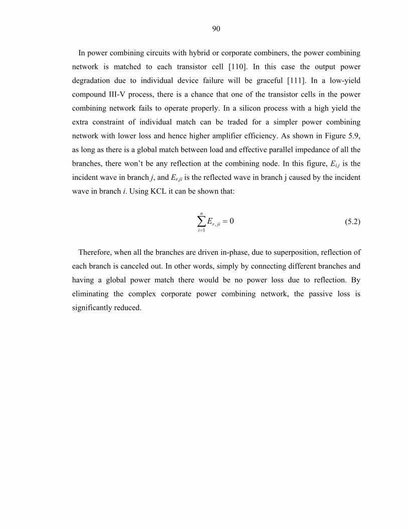
90
In power combining circuits with hybrid or corporate combiners, the power combining
network is matched to each transistor cell [110]. In this case the output power
degradation due to individual device failure will be graceful [111]. In a low-yield
compound III-V process, there is a chance that one of the transistor cells in the power
combining network fails to operate properly. In a silicon process with a high yield the
extra constraint of individual match can be traded for a simpler power combining
network with lower loss and hence higher amplifier efficiency. As shown in Figure 5.9,
as long as there is a global match between load and effective parallel impedance of all the
branches, there won’t be any reflection at the combining node. In this figure, Ei,j is the
incident wave in branch j, and Er,ji is the reflected wave in branch j caused by the incident
wave in branch i. Using KCL it can be shown that:
01
, =∑=
n
ijirE (5.2)
Therefore, when all the branches are driven in-phase, due to superposition, reflection of
each branch is canceled out. In other words, simply by connecting different branches and
having a global power match there would be no power loss due to reflection. By
eliminating the complex corporate power combining network, the passive loss is
significantly reduced.
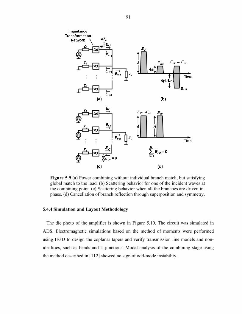
91
Figure 5.9 (a) Power combining without individual branch match, but satisfying global match to the load. (b) Scattering behavior for one of the incident waves at the combining point. (c) Scattering behavior when all the branches are driven in-phase. (d) Cancellation of branch reflection through superposition and symmetry.
5.4.4 Simulation and Layout Methodology
The die photo of the amplifier is shown in Figure 5.10. The circuit was simulated in
ADS. Electromagnetic simulations based on the method of moments were performed
using IE3D to design the coplanar tapers and verify transmission line models and non-
idealities, such as bends and T-junctions. Modal analysis of the combining stage using
the method described in [112] showed no sign of odd-mode instability.
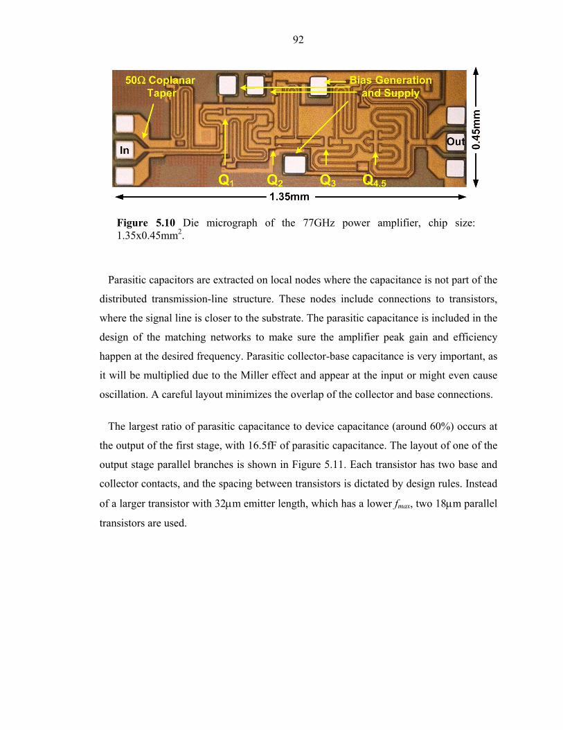
92
Parasitic capacitors are extracted on local nodes where the capacitance is not part of the
distributed transmission-line structure. These nodes include connections to transistors,
where the signal line is closer to the substrate. The parasitic capacitance is included in the
design of the matching networks to make sure the amplifier peak gain and efficiency
happen at the desired frequency. Parasitic collector-base capacitance is very important, as
it will be multiplied due to the Miller effect and appear at the input or might even cause
oscillation. A careful layout minimizes the overlap of the collector and base connections.
The largest ratio of parasitic capacitance to device capacitance (around 60%) occurs at
the output of the first stage, with 16.5fF of parasitic capacitance. The layout of one of the
output stage parallel branches is shown in Figure 5.11. Each transistor has two base and
collector contacts, and the spacing between transistors is dictated by design rules. Instead
of a larger transistor with 32μm emitter length, which has a lower fmax, two 18μm parallel
transistors are used.
Figure 5.10 Die micrograph of the 77GHz power amplifier, chip size: 1.35x0.45mm2.
93
Figure 5.11 Layout of one of the output parallel branches consisting of two transistors (depicted as Q5 in the amplifier schematic and layout).
5.5 Measurement Results
The small-signal gain of the amplifier has been measured with an HP 8757E scalar
network analyzer. The network analyzer sweeps the output frequency of a high-power W-
band back-wave oscillator (BWO) from Resonance Instruments, Inc. This is done with a
705B millimeter wave sweeper from Micro-Now Instrument Co. The signal is fed
through a WR-10 waveguide to a Pico-Probe WR-10 GSG probe. To calibrate the
network analyzer, first a thru measurement was done, and then the thru was replaced by
PA. As shown in Figure 5.12, to measure large-signal parameters of the amplifier, a
similar setup that included a variable attenuator (Millitech DRA-10-R000) with an
Agilent W8486A W-band power sensor was used. The loss of the probe was measured
and de-embedded.
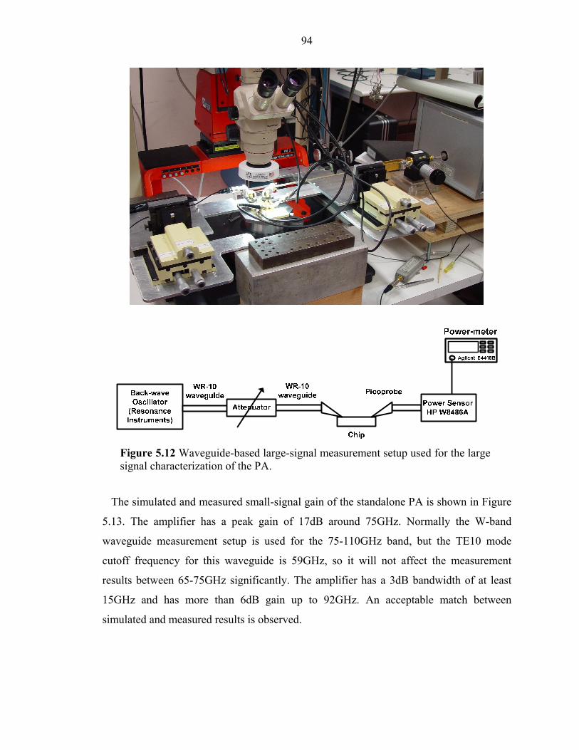
94
Figure 5.12 Waveguide-based large-signal measurement setup used for the large signal characterization of the PA.
The simulated and measured small-signal gain of the standalone PA is shown in Figure
5.13. The amplifier has a peak gain of 17dB around 75GHz. Normally the W-band
waveguide measurement setup is used for the 75-110GHz band, but the TE10 mode
cutoff frequency for this waveguide is 59GHz, so it will not affect the measurement
results between 65-75GHz significantly. The amplifier has a 3dB bandwidth of at least
15GHz and has more than 6dB gain up to 92GHz. An acceptable match between
simulated and measured results is observed.
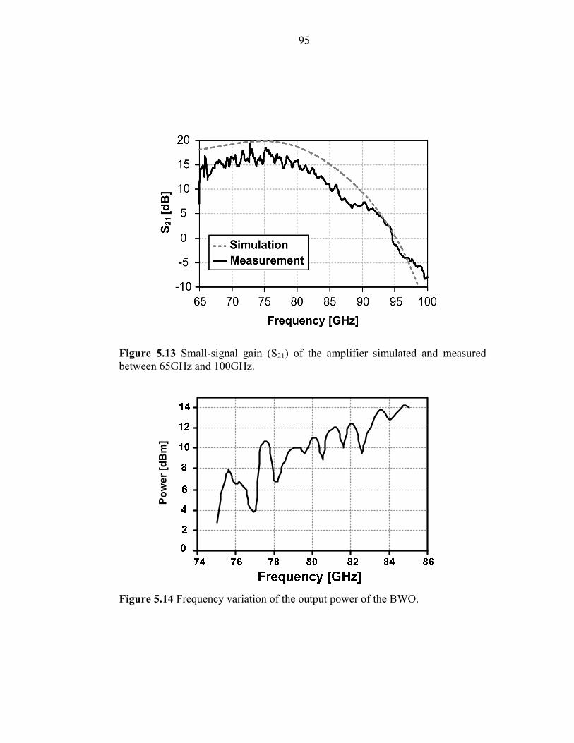
95
Figure 5.13 Small-signal gain (S21) of the amplifier simulated and measured between 65GHz and 100GHz.
Pow
er [d
Bm
]
Figure 5.14 Frequency variation of the output power of the BWO.
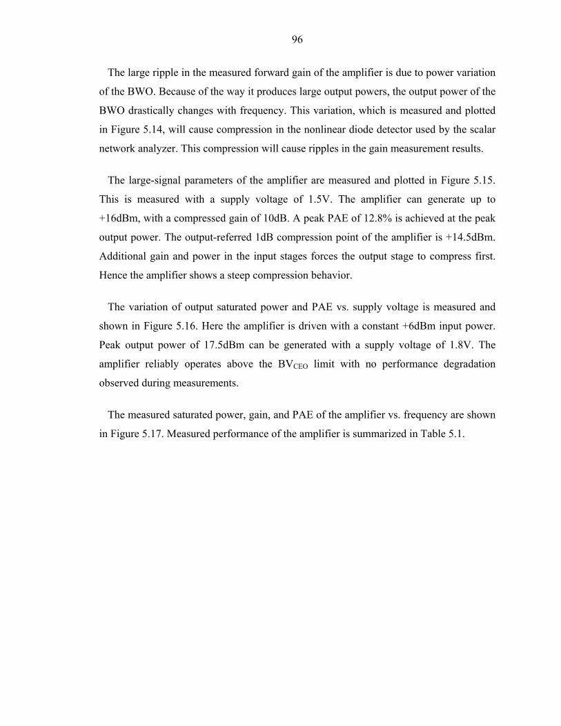
96
The large ripple in the measured forward gain of the amplifier is due to power variation
of the BWO. Because of the way it produces large output powers, the output power of the
BWO drastically changes with frequency. This variation, which is measured and plotted
in Figure 5.14, will cause compression in the nonlinear diode detector used by the scalar
network analyzer. This compression will cause ripples in the gain measurement results.
The large-signal parameters of the amplifier are measured and plotted in Figure 5.15.
This is measured with a supply voltage of 1.5V. The amplifier can generate up to
+16dBm, with a compressed gain of 10dB. A peak PAE of 12.8% is achieved at the peak
output power. The output-referred 1dB compression point of the amplifier is +14.5dBm.
Additional gain and power in the input stages forces the output stage to compress first.
Hence the amplifier shows a steep compression behavior.
The variation of output saturated power and PAE vs. supply voltage is measured and
shown in Figure 5.16. Here the amplifier is driven with a constant +6dBm input power.
Peak output power of 17.5dBm can be generated with a supply voltage of 1.8V. The
amplifier reliably operates above the BVCEO limit with no performance degradation
observed during measurements.
The measured saturated power, gain, and PAE of the amplifier vs. frequency are shown
in Figure 5.17. Measured performance of the amplifier is summarized in Table 5.1.
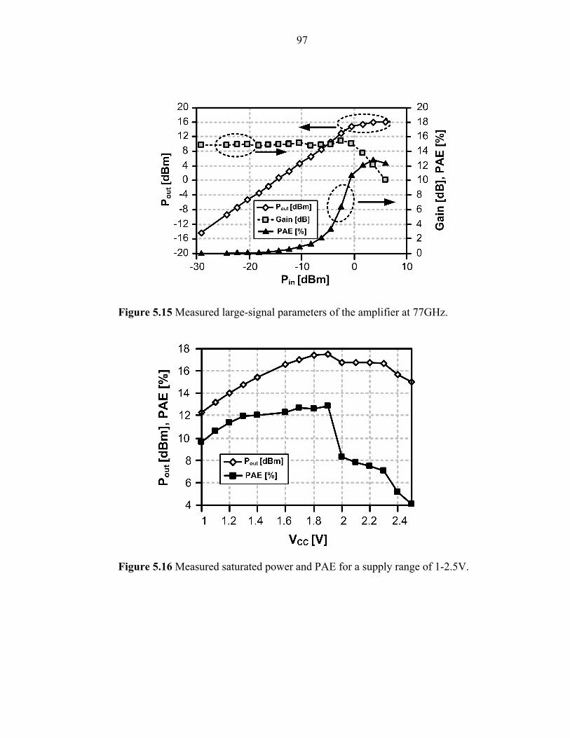
97
Figure 5.15 Measured large-signal parameters of the amplifier at 77GHz.
Figure 5.16 Measured saturated power and PAE for a supply range of 1-2.5V.

98
Figure 5.17 Measured saturated power, gain, and PAE versus frequency.
Table 5.1 Amplifier Performance Summary
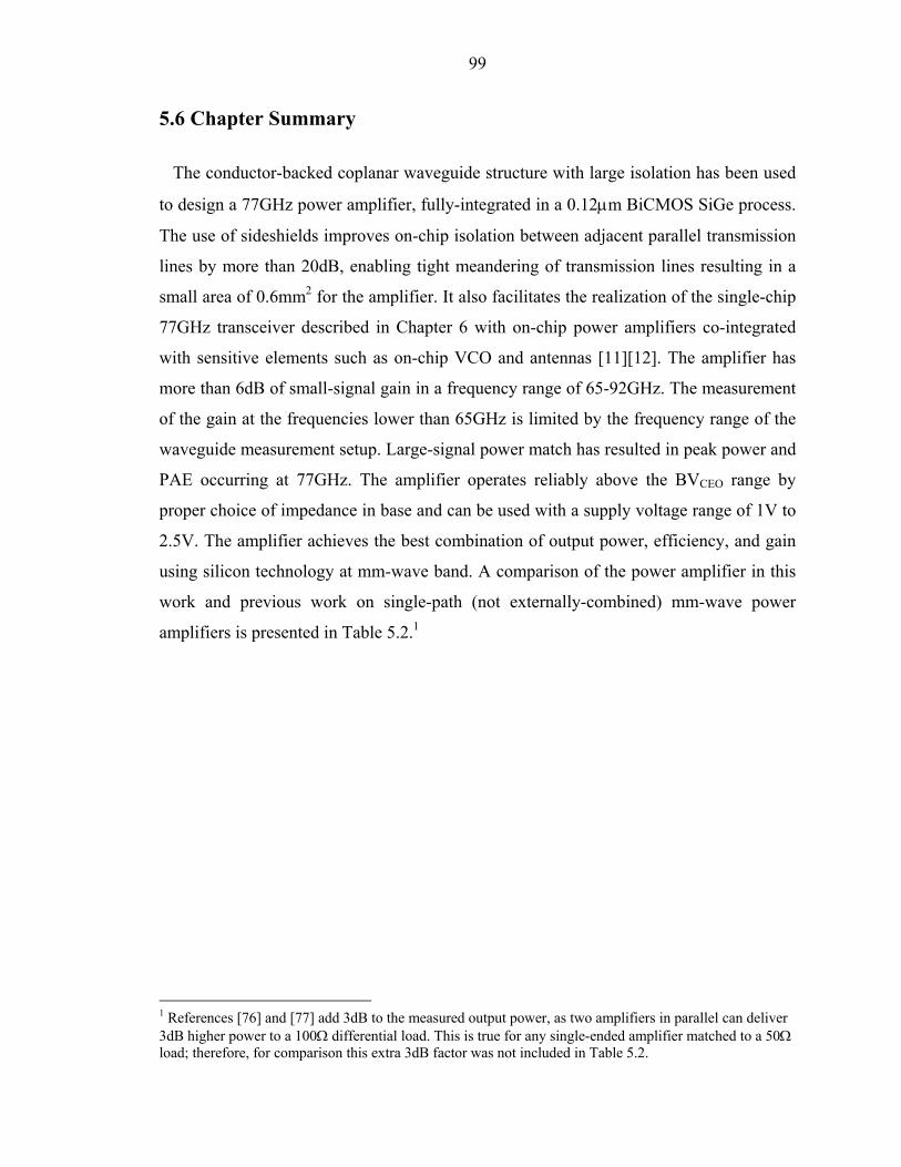
99
5.6 Chapter Summary
The conductor-backed coplanar waveguide structure with large isolation has been used
to design a 77GHz power amplifier, fully-integrated in a 0.12μm BiCMOS SiGe process.
The use of sideshields improves on-chip isolation between adjacent parallel transmission
lines by more than 20dB, enabling tight meandering of transmission lines resulting in a
small area of 0.6mm2 for the amplifier. It also facilitates the realization of the single-chip
77GHz transceiver described in Chapter 6 with on-chip power amplifiers co-integrated
with sensitive elements such as on-chip VCO and antennas [11][12]. The amplifier has
more than 6dB of small-signal gain in a frequency range of 65-92GHz. The measurement
of the gain at the frequencies lower than 65GHz is limited by the frequency range of the
waveguide measurement setup. Large-signal power match has resulted in peak power and
PAE occurring at 77GHz. The amplifier operates reliably above the BVCEO range by
proper choice of impedance in base and can be used with a supply voltage range of 1V to
2.5V. The amplifier achieves the best combination of output power, efficiency, and gain
using silicon technology at mm-wave band. A comparison of the power amplifier in this
work and previous work on single-path (not externally-combined) mm-wave power
amplifiers is presented in Table 5.2.1
1 References [76] and [77] add 3dB to the measured output power, as two amplifiers in parallel can deliver 3dB higher power to a 100Ω differential load. This is true for any single-ended amplifier matched to a 50Ω load; therefore, for comparison this extra 3dB factor was not included in Table 5.2.
100
Table 5.2 Comparison between this work and previously reported integrated high-frequency PAs.
101
Chapter 6 A 77GHz Fully-Integrated Phased-Array Transceiver
A 77GHz Fully-Integrated Phased-Array Transceiver1
The improvements in the signal-to-noise-plus-interference ratio provided by phased-
arrays and the larger bandwidths available at high frequencies motivate the
implementation of phased-arrays at higher carrier frequencies such as 24GHz, 60GHz,
and 77GHz [9][33][60][64][76]. Additionally, the array gain in a phased-array transmitter
results in a higher effective isotropic radiated power (EIRP), providing a means to
generate large powers at high frequencies. The implementation of such a high-frequency
system on a silicon-based process enables the realization of a complex SOC with
improved performance and reliability, promising a future of low-cost radar and gigabit-
per-second wireless connectivity.
In this chapter, the transmitter section of a 4-element phased-array transceiver at
77GHz is presented. The transmitter section described is part of a complete 77GHz
phased-array transceiver with integrated on-chip dipole antennas [11][12]. The LO-path
phase shift is based on a local LO phase-shifting architecture. The phase-shift resolution
in this architecture is limited by the resolution of the off-chip Digital–to-Analog
Converters (DACs), and hence this transmitter is capable of providing the fine beam-
steering resolution necessary for long-range car radar systems operating at 77GHz.
Though the 76-77GHz band is reserved for automobile sensing application, the system
concept presented in this chapter can also be applied for the Gigbit wireless application at
the 60GHz band.
Compared to the first generation of these systems, which were designed for the short-
1 The 77GHz phased-array transceiver is a joint work done by Abbas Komijani, Xiang Guan, Arun Natarajan, and Aydin Babakhani. The main focus of this chapter is the part designed by the author.
102
range car radar and point-to-point wireless communication applications in the 24GHz
band, the new phased-array architecture achieves finer resolution of phase shifting,
enabling higher angular resolution. Although the intended bandwidth for these sensors is
1GHz, having a larger bandwidth for the transmitter (2.5GHz) enables finer radial
resolution and helps mitigate the effects of process variation.
The project motivations and goals are briefly introduced in Section 6.1. The local LO-
path phase shifting architecture, an improved version of phase shifting in LO path
compared to the approach in Chapter 4, is discussed in Section 6.2. The architecture of
the transmitter is detailed in Section 6.3. Section 6.4 describes the design of the building
blocks, followed by measurement results in Section 6.5. Section 6.6 summarizes the
chapter with conclusion.
6.1 Introduction
The concept and application of automotive radar were introduced in Section 2.5. The
operation frequency approved by the FCC for such applications includes the 22-to- 29-
GHz range for ultra-wide band (UWB) short-range radar [35][36] and the 76-to-77-GHz
for frequency-modulated continuous wave (FMCW), or pulse-Doppler radar suitable for
long-range operation [34]. In addition, the Electronic Communications Committee (ECC)
within the European Conference of Postal and Telecommunications Administrations
(CEPT) has granted a 77-to-81-GHz window for automotive UWB short-range radar
since 2005 [113].
In comparison with the 24-GHz band, the 77-GHz band operation provides the
following advantages: 1) Operating at a higher frequency results in reduced antenna size
and compact package. In particular, the wavelength at 77GHz on silicon is at the same
order of chip size, making an on-chip antenna a possibility. This will significantly reduce
the cost of packaging and will eliminate the associated parasitic effects. 2) Using the 77-
GHz band for automotive radar application is a global trend, while the 24GHz UWB
band is not available in every country. 3) A concern for utilizing 24GHz for consumer
radio location is that it can potentially degrade meteorological and related environmental
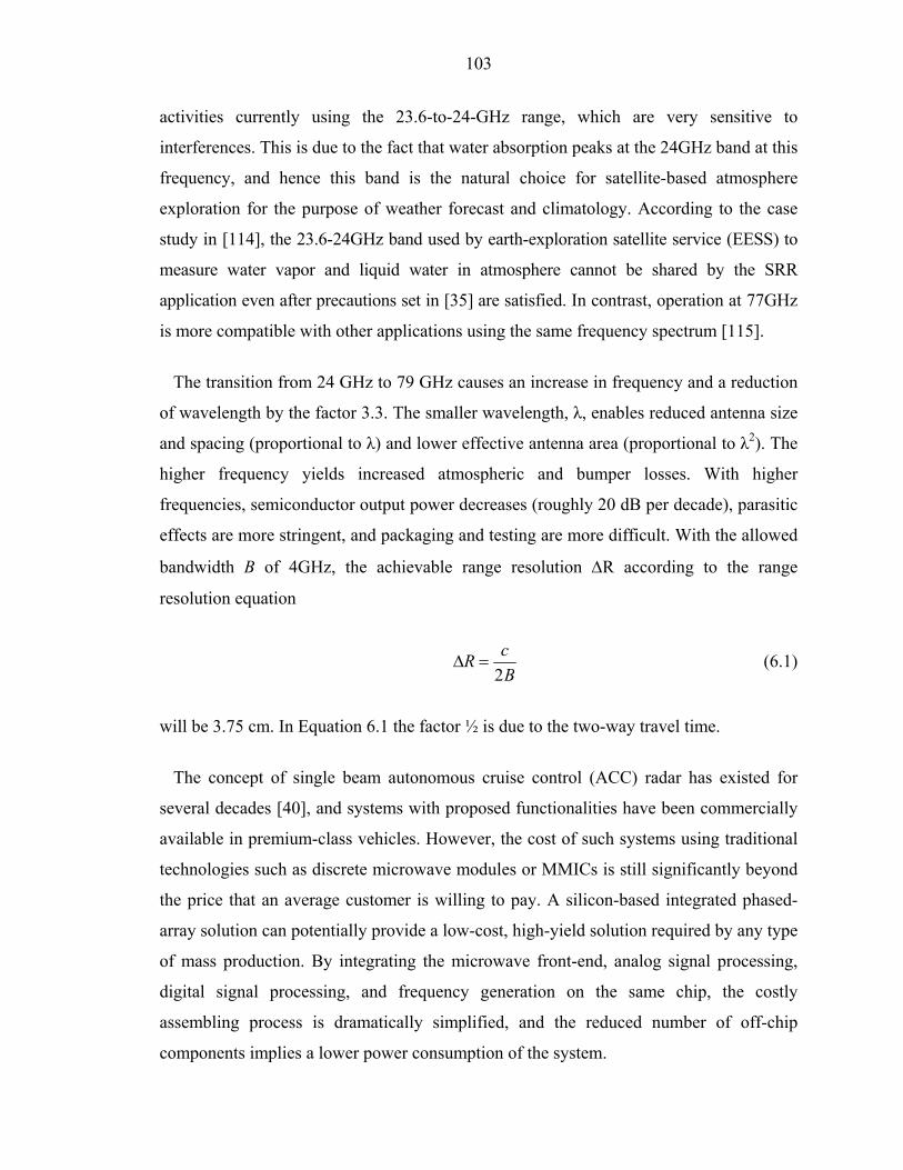
103
activities currently using the 23.6-to-24-GHz range, which are very sensitive to
interferences. This is due to the fact that water absorption peaks at the 24GHz band at this
frequency, and hence this band is the natural choice for satellite-based atmosphere
exploration for the purpose of weather forecast and climatology. According to the case
study in [114], the 23.6-24GHz band used by earth-exploration satellite service (EESS) to
measure water vapor and liquid water in atmosphere cannot be shared by the SRR
application even after precautions set in [35] are satisfied. In contrast, operation at 77GHz
is more compatible with other applications using the same frequency spectrum [115].
The transition from 24 GHz to 79 GHz causes an increase in frequency and a reduction
of wavelength by the factor 3.3. The smaller wavelength, λ, enables reduced antenna size
and spacing (proportional to λ) and lower effective antenna area (proportional to λ2). The
higher frequency yields increased atmospheric and bumper losses. With higher
frequencies, semiconductor output power decreases (roughly 20 dB per decade), parasitic
effects are more stringent, and packaging and testing are more difficult. With the allowed
bandwidth B of 4GHz, the achievable range resolution ΔR according to the range
resolution equation
BcR
2=Δ (6.1)
will be 3.75 cm. In Equation 6.1 the factor ½ is due to the two-way travel time.
The concept of single beam autonomous cruise control (ACC) radar has existed for
several decades [40], and systems with proposed functionalities have been commercially
available in premium-class vehicles. However, the cost of such systems using traditional
technologies such as discrete microwave modules or MMICs is still significantly beyond
the price that an average customer is willing to pay. A silicon-based integrated phased-
array solution can potentially provide a low-cost, high-yield solution required by any type
of mass production. By integrating the microwave front-end, analog signal processing,
digital signal processing, and frequency generation on the same chip, the costly
assembling process is dramatically simplified, and the reduced number of off-chip
components implies a lower power consumption of the system.
104
Although the current efforts at the 77-GHz range are focused on automotive radar, the
77-GHz phased-array can potentially be used for other applications, such as short-range
surveillance, microwave imaging, and ultra high-speed data transmission. The objective
of this project is to demonstrate a general purpose fully-integrated phased-array
transceiver operating at 76 – 81 GHz that can be used in both wireless communication
and short range radar. The design challenges of such systems include accurately
modeling the components and parasitic at microwave range; routing the microwave
signal over high-loss silicon substrate; finding appropriate methods to perform signal
combining, signal distribution and phase shifting; achieving a low noise performance at
receiver and providing sufficient W-band output power at transmitter; implementing
ultra-high speed frequency generating blocks such as VCO and frequency divider; and
realizing highly efficient on-chip antennas.
6.2 Local LO-Path Phase-Shifting Architecture
The phase-shifting capability required in each element of a phased-array transmitter can
be implemented in myriad ways. The tradeoffs of implementing the phase-shift at
different points in the transmit or receive chain were discussed in Section 2.6.2. Phase-
shifting in the LO-path is considered advantageous since the circuits in the LO-path
operate in saturation, and therefore it is relatively simple to ensure that the gain of each
element does not vary with the phase-shift setting. Additionally, the requirements on
phase-shifter linearity, noise figure, and bandwidth are substantially reduced when LO-
path phase-shifting is adopted.
Earlier integrated phased-array receiver and transmitter designs introduced a
centralized LO-path phase-shifting scheme in which an m-phase VCO generates multiple
phases of the LO, as shown in Figure 6.1 [9][49]. These multiple phases are then
distributed to the phase-selector in each element which selects the appropriate phase of
the LO for the desired beam-direction. One limitation with this approach stems from the
fact that the phase-resolution is limited by the number of phases generated by the VCO.
Another limitation, more important at mm-wave frequencies, arises from the necessity to
distribute all the LO phases to each element. This necessity to distribute a large number
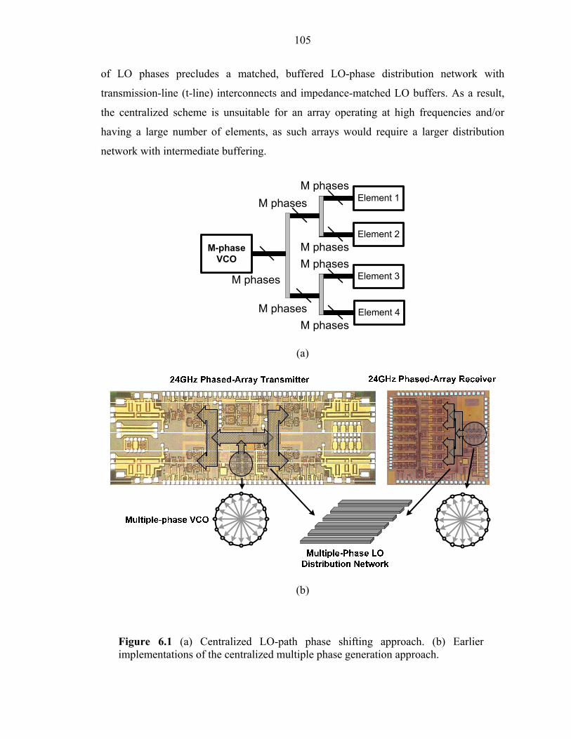
105
of LO phases precludes a matched, buffered LO-phase distribution network with
transmission-line (t-line) interconnects and impedance-matched LO buffers. As a result,
the centralized scheme is unsuitable for an array operating at high frequencies and/or
having a large number of elements, as such arrays would require a larger distribution
network with intermediate buffering.
M phases
M phasesM phases
M phases
M phases
M phases
M phases
Element 1
Element 2
Element 3
Element 4
M-phaseVCO
(a)
(b)
Figure 6.1 (a) Centralized LO-path phase shifting approach. (b) Earlier implementations of the centralized multiple phase generation approach.
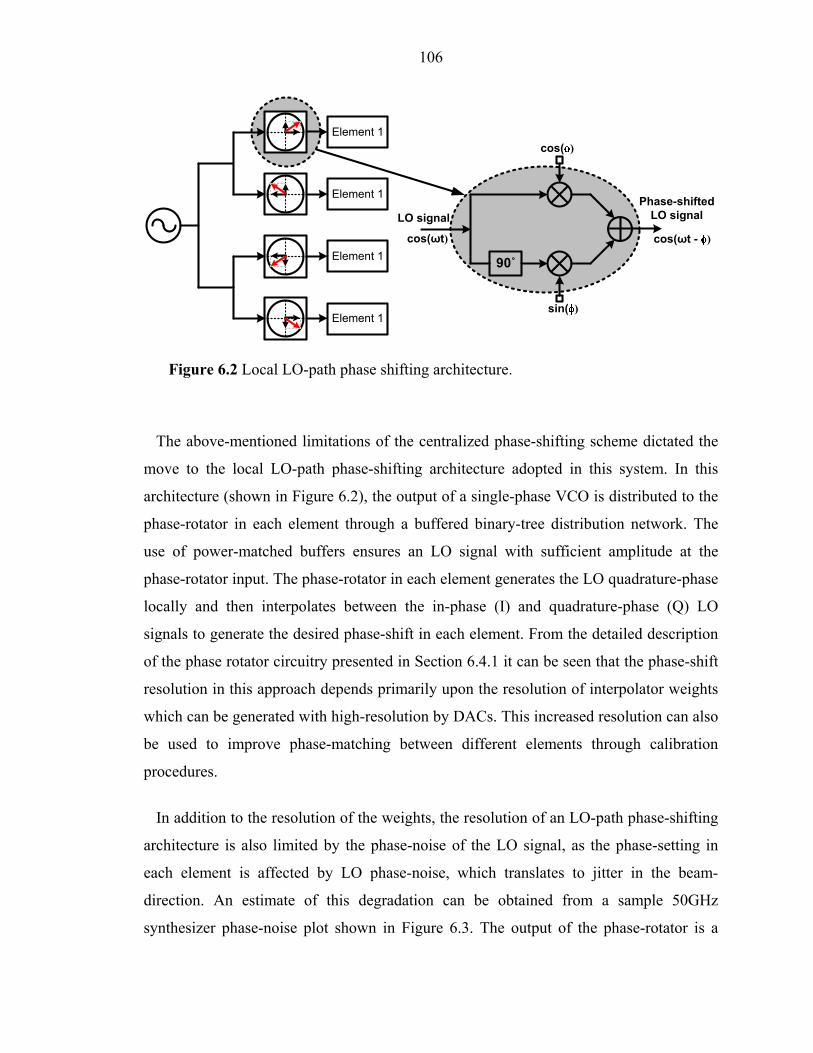
106
The above-mentioned limitations of the centralized phase-shifting scheme dictated the
move to the local LO-path phase-shifting architecture adopted in this system. In this
architecture (shown in Figure 6.2), the output of a single-phase VCO is distributed to the
phase-rotator in each element through a buffered binary-tree distribution network. The
use of power-matched buffers ensures an LO signal with sufficient amplitude at the
phase-rotator input. The phase-rotator in each element generates the LO quadrature-phase
locally and then interpolates between the in-phase (I) and quadrature-phase (Q) LO
signals to generate the desired phase-shift in each element. From the detailed description
of the phase rotator circuitry presented in Section 6.4.1 it can be seen that the phase-shift
resolution in this approach depends primarily upon the resolution of interpolator weights
which can be generated with high-resolution by DACs. This increased resolution can also
be used to improve phase-matching between different elements through calibration
procedures.
In addition to the resolution of the weights, the resolution of an LO-path phase-shifting
architecture is also limited by the phase-noise of the LO signal, as the phase-setting in
each element is affected by LO phase-noise, which translates to jitter in the beam-
direction. An estimate of this degradation can be obtained from a sample 50GHz
synthesizer phase-noise plot shown in Figure 6.3. The output of the phase-rotator is a
Element 1
Element 1
Element 1
Element 1
90˚
cos( )
sin( )
LO signal
cos(ωt - )
Phase-shiftedLO signal
cos(ωt)
Figure 6.2 Local LO-path phase shifting architecture.
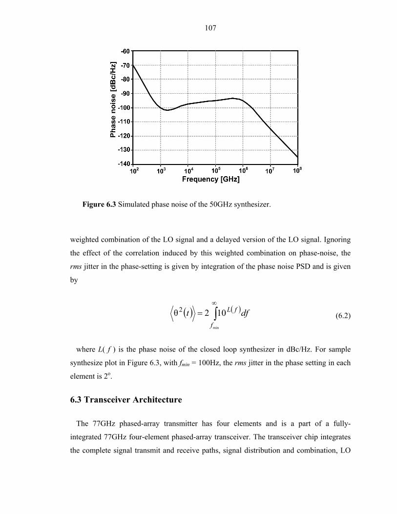
107
weighted combination of the LO signal and a delayed version of the LO signal. Ignoring
the effect of the correlation induced by this weighted combination on phase-noise, the
rms jitter in the phase-setting is given by integration of the phase noise PSD and is given
by
( ) ( )dftf
fL∫∞
=min
102θ2 (6.2)
where L( f ) is the phase noise of the closed loop synthesizer in dBc/Hz. For sample
synthesize plot in Figure 6.3, with fmin = 100Hz, the rms jitter in the phase setting in each
element is 2o.
6.3 Transceiver Architecture
The 77GHz phased-array transmitter has four elements and is a part of a fully-
integrated 77GHz four-element phased-array transceiver. The transceiver chip integrates
the complete signal transmit and receive paths, signal distribution and combination, LO
Figure 6.3 Simulated phase noise of the 50GHz synthesizer.
108
signal generation and distribution, phase rotating elements, and 77-GHz antenna on a
single silicon die.
The architecture of the transceiver is shown in Figure 6.4. The LO frequency
generation circuits are shared between the receiver and the transmitter. It is important to
note that each transmit and receive element includes an independent phase-rotator that
applies the desired phase of the LO to the upconversion or downconversion mixer.
The transceiver utilizes a two-step up/down conversion scheme with an IF frequency of
26GHz. The on-chip VCO generates the 52GHz LO signal necessary for the second
upconversion in the TX path (and for the first downconversion in RX path), while the
quadrature 26GHz signal required for the first upconversion (and second downconversion
in RX) is provided by an injection-locked divide-by-two following the VCO.
It’s important to point that the frequency plan of this system allows for the development
of a dual-mode automotive radar system. The first mode is operating at the 76-to-81 GHz
radar band, and the second mode is operating at the 22-to-29 GHz radar band by
bypassing the RF part and directly tapping out the IF output at 26GHz. Thus, this general
system can utilize both radar bands for short and long-range radar applications.
In the transmit signal path, the baseband signals are upconverted to 26GHz by a pair of
quadrature upconversion mixers. The signal distribution to all the elements is done at IF
through a network of distribution amplifiers. The RF mixer in each element upconverts
the 26GHz input signal to 77GHz, providing the input for a driver that feeds on-chip
77GHz power amplifiers. The signal is boosted to the desired level by PAs and is radiated
off with an on-chip dipole antenna. The adopted frequency plan leads to the image of the
second upconversion falling at 26GHz, while the RF is at 77GHz. The tuned mixer,
driver, power amplifier, and antenna provide sufficient attenuation at the image
frequency; therefore, the second upconversion does not employ an image-reject
architecture.
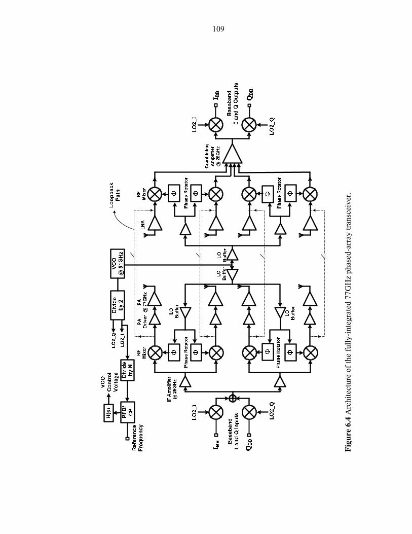
109
Figu
re 6
.4 A
rchi
tect
ure
of th
e fu
lly-in
tegr
ated
77G
Hz
phas
ed-a
rray
tran
scei
ver.
110
The receiver uses a frequency plan similar to the transmitter so that they can share the
same frequency generation circuitry. Each RF front-end consists of an on-chip dipole
antenna, LNA, mixer, and IF amplifier. The phase shifting is performed at the LO port of
the mixer at 52-GHz with an analog phase rotator. By switching the digital control bit,
the gain of the IF amplifier can be varied by 15dB so that the system dynamic range is
enhanced. The 26-GHz signals are combined using a symmetric active combining
amplifier. The combined signal is further downconverted using a quadrature IF-to-
baseband mixer.
A loop-back mode is also created on-chip, directly connecting the output of the RF
mixer in the transmitter to the input of the RF mixer in the receiver in each path. When
the chip is switched to this mode, a four-input-four-output upconversion-downconversion
link is formed, which can be used to perform baseband to baseband measurement with no
high-frequency off-chip connections. This measurement is particularly convenient and
informative in evaluating the array pattern, beam steering, and data-rate capabilities of
the system.
In the LO path, the output of the differential, cross-coupled 52GHz VCO is distributed
to the phase-rotators in each element through a symmetric network of distribution buffers
that ensure that the phase of the LO signal is the same at the input of the phase rotator in
all transmit elements. Phase rotators in each element generate the desired phase shift in
the LO path for each element. To reduce the VCO power and area-cost of the LO
distribution network, only a differential phase is generated by the core oscillator and
distributed across the chip. The required quadrature component of the LO signal, which is
needed to perform interpolation, is done locally.
The transmission line loss on the LO distribution network is compensated by the inter-
link LO buffers. The continuous phase rotation performed locally allows for continuous
beam steering capability and accurate compensation of the phase and amplitude
mismatch between paths caused by the asymmetry in phase distribution and antenna
elements. A cascade of divide-by-two frequency divider blocks following the VCO
generates the 50MHz signal that is used by an off-chip PFD to lock the VCO.
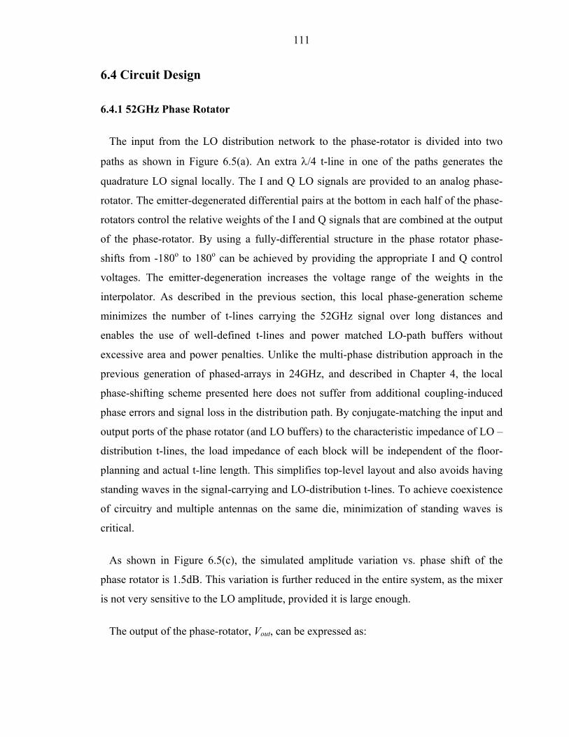
111
6.4 Circuit Design
6.4.1 52GHz Phase Rotator
The input from the LO distribution network to the phase-rotator is divided into two
paths as shown in Figure 6.5(a). An extra λ/4 t-line in one of the paths generates the
quadrature LO signal locally. The I and Q LO signals are provided to an analog phase-
rotator. The emitter-degenerated differential pairs at the bottom in each half of the phase-
rotators control the relative weights of the I and Q signals that are combined at the output
of the phase-rotator. By using a fully-differential structure in the phase rotator phase-
shifts from -180o to 180o can be achieved by providing the appropriate I and Q control
voltages. The emitter-degeneration increases the voltage range of the weights in the
interpolator. As described in the previous section, this local phase-generation scheme
minimizes the number of t-lines carrying the 52GHz signal over long distances and
enables the use of well-defined t-lines and power matched LO-path buffers without
excessive area and power penalties. Unlike the multi-phase distribution approach in the
previous generation of phased-arrays in 24GHz, and described in Chapter 4, the local
phase-shifting scheme presented here does not suffer from additional coupling-induced
phase errors and signal loss in the distribution path. By conjugate-matching the input and
output ports of the phase rotator (and LO buffers) to the characteristic impedance of LO –
distribution t-lines, the load impedance of each block will be independent of the floor-
planning and actual t-line length. This simplifies top-level layout and also avoids having
standing waves in the signal-carrying and LO-distribution t-lines. To achieve coexistence
of circuitry and multiple antennas on the same die, minimization of standing waves is
critical.
As shown in Figure 6.5(c), the simulated amplitude variation vs. phase shift of the
phase rotator is 1.5dB. This variation is further reduced in the entire system, as the mixer
is not very sensitive to the LO amplitude, provided it is large enough.
The output of the phase-rotator, Vout, can be expressed as:
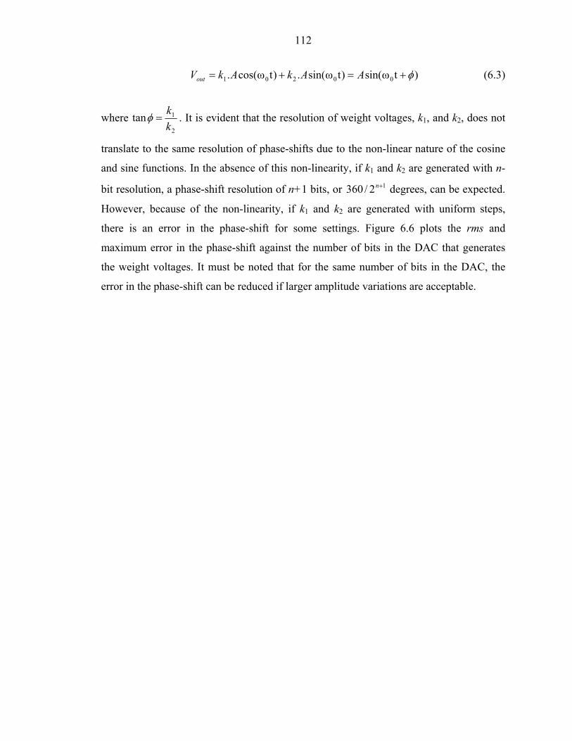
112
)t ωsin()tωsin(.)tωcos(. 00201 φ+=+= AAkAkVout (6.3)
where2
1tankk
=φ . It is evident that the resolution of weight voltages, k1, and k2, does not
translate to the same resolution of phase-shifts due to the non-linear nature of the cosine
and sine functions. In the absence of this non-linearity, if k1 and k2 are generated with n-
bit resolution, a phase-shift resolution of n+1 bits, or 12/360 +n degrees, can be expected.
However, because of the non-linearity, if k1 and k2 are generated with uniform steps,
there is an error in the phase-shift for some settings. Figure 6.6 plots the rms and
maximum error in the phase-shift against the number of bits in the DAC that generates
the weight voltages. It must be noted that for the same number of bits in the DAC, the
error in the phase-shift can be reduced if larger amplitude variations are acceptable.
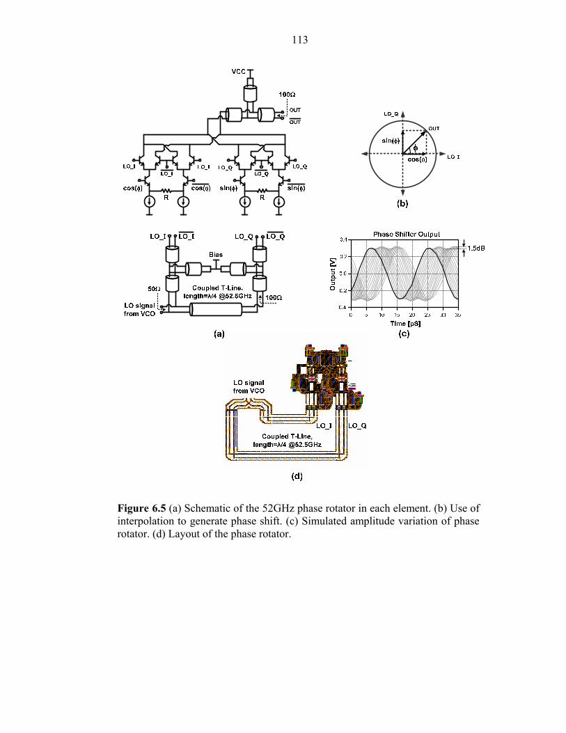
113
Figure 6.5 (a) Schematic of the 52GHz phase rotator in each element. (b) Use of interpolation to generate phase shift. (c) Simulated amplitude variation of phase rotator. (d) Layout of the phase rotator.
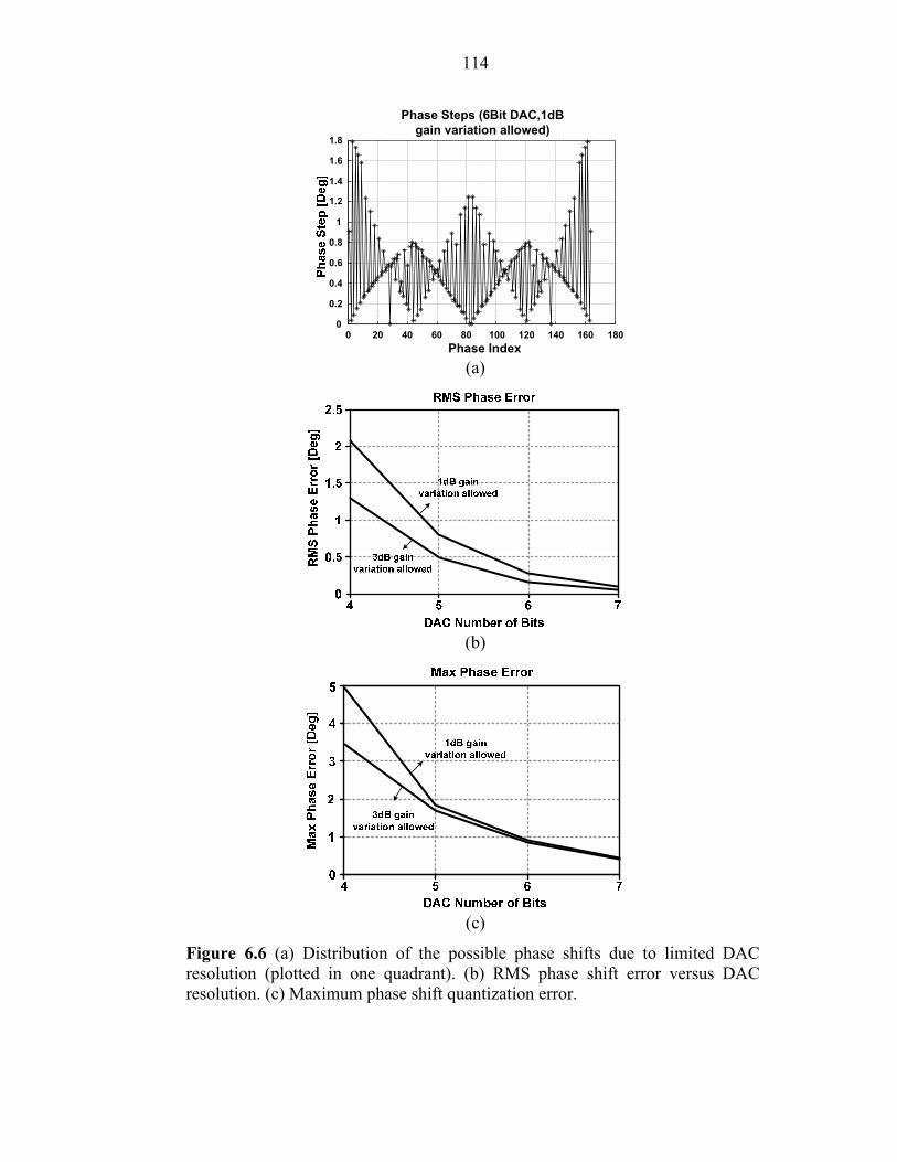
114
0 20 40 60 80 100 120 140 160 180
Phase Steps (6Bit DAC,1dB gain variation allowed)
0
0.2
0.4
0.6
0.8
1
1.2
1.4
1.6
1.8
Phase Index (a)
(b)
(c)
Figure 6.6 (a) Distribution of the possible phase shifts due to limited DAC resolution (plotted in one quadrant). (b) RMS phase shift error versus DAC resolution. (c) Maximum phase shift quantization error.
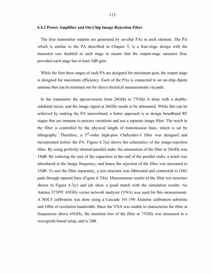
115
6.4.2 Power Amplifier and On-Chip Image-Rejection Filter
The four transmitter outputs are generated by on-chip PAs in each element. The PA
which is similar to the PA described in Chapter 5, is a four-stage design with the
transistor size doubled in each stage to ensure that the output-stage saturates first,
provided each stage has at least 3dB gain.
While the first three stages of each PA are designed for maximum gain, the output stage
is designed for maximum efficiency. Each of the PAs is connected to an on-chip dipole
antenna that can be trimmed out for direct electrical measurements via pads.
In the transmitter the upconversion from 26GHz to 77GHz is done with a double-
sideband mixer, and the image signal at 26GHz needs to be attenuated. While this can be
achieved by making the PA narrowband, a better approach is to design broadband RF
stages that are immune to process variations and use a separate image filter. The notch in
the filter is controlled by the physical length of transmission lines, which is set by
lithography. Therefore, a 3rd-order high-pass Chebyshev-I filter was designed and
incorporated before the PA. Figure 6.7(a) shows the schematics of the image-rejection
filter. By using perfectly-shorted parallel stubs, the attenuation of the filter at 26GHz was
18dB. By reducing the size of the capacitors at the end of the parallel stubs, a notch was
introduced at the image frequency, and hence the rejection of the filter was increased to
35dB. To test the filter separately, a test structure was fabricated and connected to GSG
pads through tapered lines (Figure 6.7(b)). Measurement results of the filter test structure
shown in Figure 6.7(c) and (d) show a good match with the simulation results. An
Anritsu 37397C 65GHz vector network analyzer (VNA) was used for this measurement.
A SOLT calibration was done using a Cascade 101-190 Alumina calibration substrate
and 10Hz of resolution bandwidth. Since the VNA was unable to characterize the filter at
frequencies above 65GHz, the insertion loss of the filter at 77GHz was measured in a
waveguide-based setup, and is 2dB.
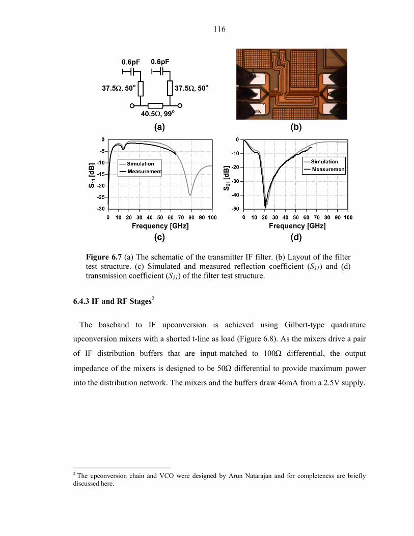
116
Figure 6.7 (a) The schematic of the transmitter IF filter. (b) Layout of the filter test structure. (c) Simulated and measured reflection coefficient (S11) and (d) transmission coefficient (S21) of the filter test structure.
6.4.3 IF and RF Stages2
The baseband to IF upconversion is achieved using Gilbert-type quadrature
upconversion mixers with a shorted t-line as load (Figure 6.8). As the mixers drive a pair
of IF distribution buffers that are input-matched to 100Ω differential, the output
impedance of the mixers is designed to be 50Ω differential to provide maximum power
into the distribution network. The mixers and the buffers draw 46mA from a 2.5V supply.
2 The upconversion chain and VCO were designed by Arun Natarajan and for completeness are briefly discussed here.
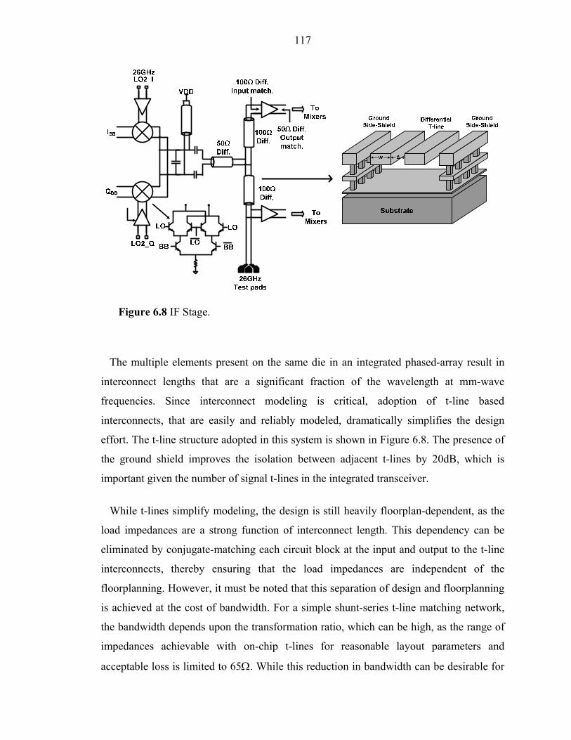
117
The multiple elements present on the same die in an integrated phased-array result in
interconnect lengths that are a significant fraction of the wavelength at mm-wave
frequencies. Since interconnect modeling is critical, adoption of t-line based
interconnects, that are easily and reliably modeled, dramatically simplifies the design
effort. The t-line structure adopted in this system is shown in Figure 6.8. The presence of
the ground shield improves the isolation between adjacent t-lines by 20dB, which is
important given the number of signal t-lines in the integrated transceiver.
While t-lines simplify modeling, the design is still heavily floorplan-dependent, as the
load impedances are a strong function of interconnect length. This dependency can be
eliminated by conjugate-matching each circuit block at the input and output to the t-line
interconnects, thereby ensuring that the load impedances are independent of the
floorplanning. However, it must be noted that this separation of design and floorplanning
is achieved at the cost of bandwidth. For a simple shunt-series t-line matching network,
the bandwidth depends upon the transformation ratio, which can be high, as the range of
impedances achievable with on-chip t-lines for reasonable layout parameters and
acceptable loss is limited to 65Ω. While this reduction in bandwidth can be desirable for
Figure 6.8 IF Stage.
118
some applications, it poses a problem for broadband applications. This challenge can be
overcome by reducing the quality-factor (Q) of the tuned loads or by using higher-order
matching networks [59]. In our design, the characteristic impedance of t-line
interconnects was generally chosen to be 50Ω to allow for probe-based measurements at
internal test points.
The 26GHz IF signal is upconverted to 77GHz by a Gilbert-type upconversion mixer in
each element (Figure 6.9). All the circuits in the transmitter up to and including the mixer
are differential, whereas the PA driver and the PA are single-ended in order to facilitate
measurements. While an on-chip mm-wave balun can be implemented, similar to [116],
area limitations did not permit that option. Therefore, one of the differential outputs of
the mixer is terminated to 50Ω through a capacitor. The other output of the mixer is fed
to the PA driver that is input matched to 50Ω.
6.4.4 52GHz Voltage-Controlled Oscillator
The 52GHz VCO, the schematic of which is shown in Figure 6.10, employs a
differential cross-coupled design. A shorted differential t-line is used as the inductor in
the tank. The proximity of the return-path in the chosen t-line reduces the inductance-per-
unit-length and increases current-crowding, which leads to lower Q of the inductor (in
Figure 6.9 RF Stage.
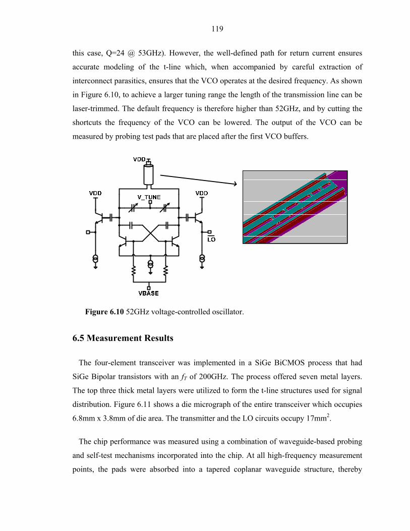
119
this case, Q=24 @ 53GHz). However, the well-defined path for return current ensures
accurate modeling of the t-line which, when accompanied by careful extraction of
interconnect parasitics, ensures that the VCO operates at the desired frequency. As shown
in Figure 6.10, to achieve a larger tuning range the length of the transmission line can be
laser-trimmed. The default frequency is therefore higher than 52GHz, and by cutting the
shortcuts the frequency of the VCO can be lowered. The output of the VCO can be
measured by probing test pads that are placed after the first VCO buffers.
Figure 6.10 52GHz voltage-controlled oscillator.
6.5 Measurement Results
The four-element transceiver was implemented in a SiGe BiCMOS process that had
SiGe Bipolar transistors with an fT of 200GHz. The process offered seven metal layers.
The top three thick metal layers were utilized to form the t-line structures used for signal
distribution. Figure 6.11 shows a die micrograph of the entire transceiver which occupies
6.8mm x 3.8mm of die area. The transmitter and the LO circuits occupy 17mm2.
The chip performance was measured using a combination of waveguide-based probing
and self-test mechanisms incorporated into the chip. At all high-frequency measurement
points, the pads were absorbed into a tapered coplanar waveguide structure, thereby

120
accounting for pad parasitics while maintaining 50Ω characteristic impedance. For
instance, both VCO and divide-by-two outputs are connected to such pad structures to
enable direct measurement.
As the transmitter measurements have to be performed at mm-wave frequencies, a
waveguide-based measurement setup is utilized for characterizing the transmitter (Figure
6.12). In the case of single-element measurements, the output of the transmitter is probed
using WR-123 probes. The output is then connected to an external downconverter which
mixes the 77GHz output down to 18GHz, making it possible to view the output on a
spectrum analyzer. As mentioned, the chip requires a 1.5V supply for the PA and the PA
driver and a 2.5V supply for the rest of the circuitry.
3 The WR-12 waveguide has a standard operating frequency range from 60GHz to 90GHz. With a cutoff frequency at 49GHz, it can be used for VCO measurements (with input frequencies larger than 50GHz).
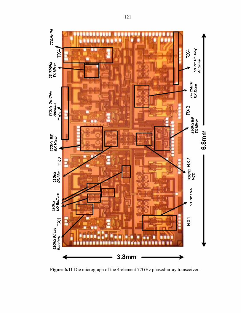
121
Figure 6.11 Die micrograph of the 4-element 77GHz phased-array transceiver.
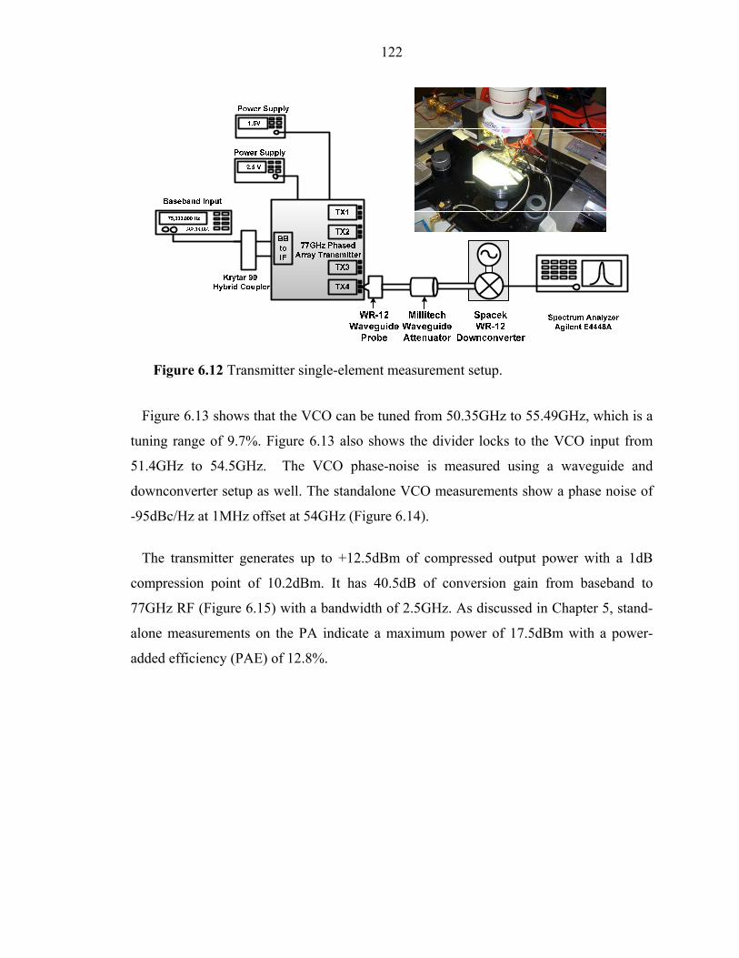
122
Figure 6.12 Transmitter single-element measurement setup.
Figure 6.13 shows that the VCO can be tuned from 50.35GHz to 55.49GHz, which is a
tuning range of 9.7%. Figure 6.13 also shows the divider locks to the VCO input from
51.4GHz to 54.5GHz. The VCO phase-noise is measured using a waveguide and
downconverter setup as well. The standalone VCO measurements show a phase noise of
-95dBc/Hz at 1MHz offset at 54GHz (Figure 6.14).
The transmitter generates up to +12.5dBm of compressed output power with a 1dB
compression point of 10.2dBm. It has 40.5dB of conversion gain from baseband to
77GHz RF (Figure 6.15) with a bandwidth of 2.5GHz. As discussed in Chapter 5, stand-
alone measurements on the PA indicate a maximum power of 17.5dBm with a power-
added efficiency (PAE) of 12.8%.

123
(a)
(b)
Figure 6.13 (a) VCO tuning range for different cutting points in the t-line. (b) VCO tuning curve (after cutting two bars) with divider locking range.
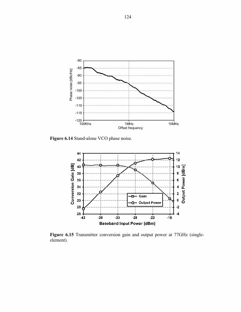
124
Figure 6.14 Stand-alone VCO phase noise.
Figure 6.15 Transmitter conversion gain and output power at 77GHz (single-element).
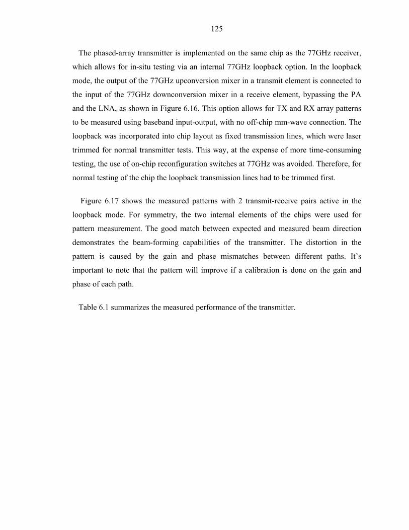
125
The phased-array transmitter is implemented on the same chip as the 77GHz receiver,
which allows for in-situ testing via an internal 77GHz loopback option. In the loopback
mode, the output of the 77GHz upconversion mixer in a transmit element is connected to
the input of the 77GHz downconversion mixer in a receive element, bypassing the PA
and the LNA, as shown in Figure 6.16. This option allows for TX and RX array patterns
to be measured using baseband input-output, with no off-chip mm-wave connection. The
loopback was incorporated into chip layout as fixed transmission lines, which were laser
trimmed for normal transmitter tests. This way, at the expense of more time-consuming
testing, the use of on-chip reconfiguration switches at 77GHz was avoided. Therefore, for
normal testing of the chip the loopback transmission lines had to be trimmed first.
Figure 6.17 shows the measured patterns with 2 transmit-receive pairs active in the
loopback mode. For symmetry, the two internal elements of the chips were used for
pattern measurement. The good match between expected and measured beam direction
demonstrates the beam-forming capabilities of the transmitter. The distortion in the
pattern is caused by the gain and phase mismatches between different paths. It’s
important to note that the pattern will improve if a calibration is done on the gain and
phase of each path.
Table 6.1 summarizes the measured performance of the transmitter.
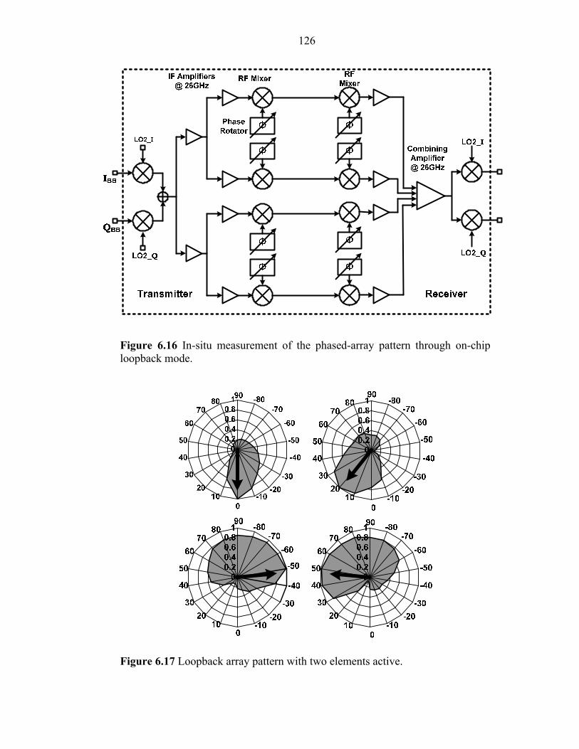
126
Figure 6.16 In-situ measurement of the phased-array pattern through on-chip loopback mode.
Figure 6.17 Loopback array pattern with two elements active.
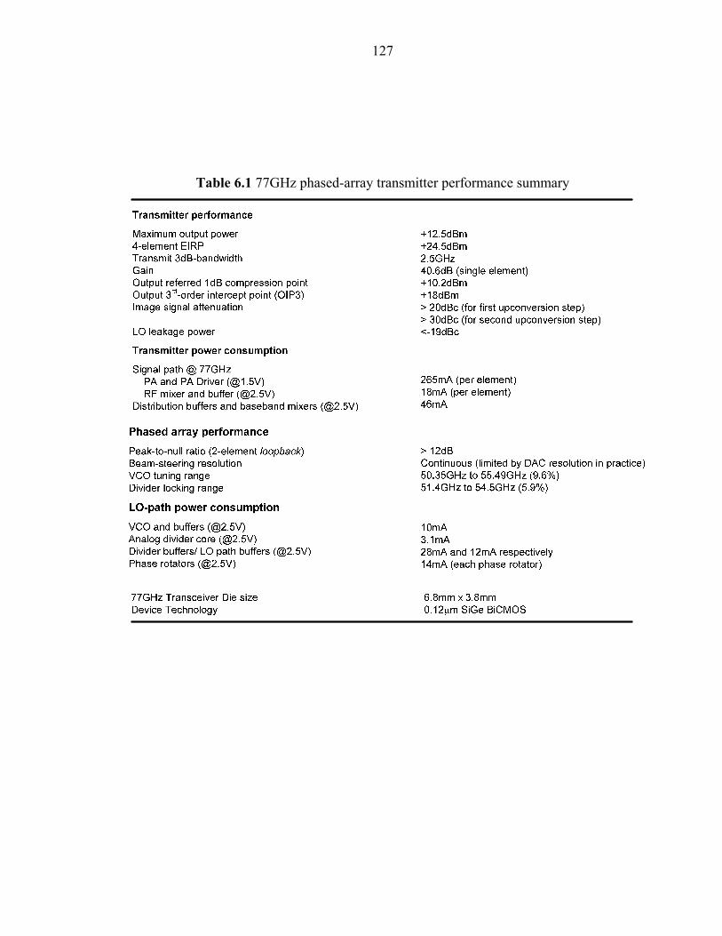
127
Table 6.1 77GHz phased-array transmitter performance summary
128
6.6 Chapter Summary
In this chapter, the transmitter and LO-path phase-shifting sections of a fully-integrated
77GHz phased-array transceiver have been presented. The transceiver employs a local
LO-path phase-shifting architecture that scales well with an increase in the number of on-
chip elements. The transmitter with on-chip power amplifiers achieves 12.5dBm output
power at 77GHz with a bandwidth of 2.5GHz. By using a separate image-rejection filter
incorporated before the PA, the rejection at IF frequency of 25GHz is improved by 35dB,
helping to keep the PA design wideband.
The on-chip VCO tunes from 50.3GGHz and 55.49GHz, and the quadrature injection-
locked divider locks from 51.4GHz to 54.5GHz. The phased-array achieves 12dB peak-
to-null ratio with 2 elements active. The complete integration of four transmit and receive
elements along with the frequency generation and phase-shifting circuitry in this
transceiver represent the highest levels of silicon integration achieved at mm-wave
frequencies.
129
Chapter 7 Conclusion
Conclusion
Phased-array systems operating at microwave frequency range provide large bandwidth,
compact antenna solution, spatial selectivity, and electronic beam steering that benefit
high-speed data transmission and radar surveillance. In this thesis various techniques to
implement such systems in low-cost, high integration level, and high-yield silicon-based
technologies were explored. Two integrated transmitters operating at the 24GHz and
77GHz range have been demonstrated in silicon for the first time.
As the first demonstration, a fully-integrated four-element 24GHz phased-array
transmitter with on-chip power amplifiers has been implemented in a 0.18μm CMOS
process. The four-bit LO-path phase-shifting approach adopted in the transmitter has
better than 10° beam-steering resolution for radiation normal to the array. Each on-chip
PA is capable of generating up to 14.5dBm output power, translating to an EIRP of
26.5dBm. The transmitter is capable of supporting data rates in excess of 500Mbps and
is well-suited for 24GHz wireless links. The fully-integrated four-element 24GHz
phased-array transmitter with on-chip power amplifiers reported in this work is not only
the first fully-integrated phased-array transmitter but also the first system to demonstrate
such levels of integration at 24GHz using 0.18µm CMOS transistors. This work
demonstrates that CMOS technology is a viable candidate for building fully-integrated
transmitters at frequencies higher than 20GHz.
In second part of this work, a 77GHz wide-band phased array transceiver has been
integrated in a SiGe HBT process providing a fT of 200GHz. In this work, on-chip
antenna is used for signal reception and radiation. The phase shifting is performed at LO
ports of the RF mixers using continuous analog phase shifters. The author’s efforts are
130
focused on the transmitter on-chip power amplifier, LO distribution network, and
continuous local phase shift circuitry. Measurement results demonstrate a 40dB
conversion gain, 2.5GHz of bandwidth, and maximum power of 12.5dBm per transmitter
element. Measured array patterns at various phase settings prove the spatial selectivity
and beam steering capability of the system.
7.1 Recommendations for Future Work
This work proves the feasibility of fully-integrated microwave phased-array
transmitters in silicon. Future trends would examine how to implement such system into
products for specified applications, such as communication, radar, and microwave
imaging, which demand more research efforts in system definition, circuit innovation and
digital signal processing. To increase the number of array elements integrated on a single
chip, more compact and lower power circuits, efficient signal and LO combining and
distribution methods, and system architectures that maximize circuits sharing need to be
developed. Among various architectures, direct conversion phased array and a phased
array with true time-domain compensation are particularly interesting for investigation.
As an improvement, on-chip calibration can be used to minimize phase and gain
mismatch of the array elements.

131
Bibliography
[1] A. A. Abidi, “RF CMOS comes of age,” IEEE Journal of Solid-State Circuits, vol.
39, no. 4, pp. 549–561, Apr. 2004.
[2] G. E. Moore, “Cramming more components onto integrated circuits,” Electronics, vol.
38, no. 8, pp. 114–117, Apr. 1965.
[3] D. Parker and D. C. Zimmermann, “Phased arrays—Part I: Theory and architectures,”
IEEE Trans. Microw. Theory Tech., vol. 50, no. 3, pp. 678–687, Mar. 2002.
[4] D. Parker and D. C. Zimmermann, “Phased arrays—Part II: Implementations,
applications, and future trends,” IEEE Trans. Microw. Theory Tech., vol. 50, no. 3, pp.
688–698, Mar. 2002.
[5] W. H. V. Aulock, “Properties of phased arrays,” Proc. IRE, vol. 48, pp. 1715–1728,
Oct. 1960.
[6] R. C. Hansen, Ed., Significant Phased Array Papers. Norwood, MA: Artech House,
1973.
[7] R. S. Elliott, Antenna Theory and Design. Englewood Cliffs, NJ: Prentice-Hall, 1981.
[8] A. Komijani and A. Hajimiri, “A 24 GHz, +14.5 dBm fully-integrated power
amplifier in 0.18 μm CMOS,” Proc. IEEE Custom Integrated Circuits Conf., Oct. 2004,
pp. 561–564.
[9] A. Natarajan, A. Komijani, and A. Hajimiri, “A 24 GHz phased-array transmitter in
0.18 μm CMOS,” IEEE Int. Solid-State Circuits Conf. (ISSCC) Dig. Tech. Papers, Feb.
2005, vol. 48, pp. 212–213.
132
[10] A. Komijani and A. Hajimiri, “A wideband 77GHz, 17.5dBm power amplifier in
silicon,” Proc. IEEE Custom Integrated Circuits Conf., Sep. 2005, pp. 571–574.
[11] A. Natarajan, A. Komijani, X. Guan, A. Babakhani, Y. Wang, and A. Hajimiri, “A
77 GHz phased array transmitter with local LO-path phase-shifting in silicon,” IEEE Int.
Solid-State Circuits Conf. (ISSCC) Dig. Tech. Papers, Feb. 2006, vol. 49, pp. 182–183.
[12] A. Babakhani, X. Guan, A. Komijani, A. Natarajan, and A. Hajimiri, “A 77 GHz 4-
element phased-array receiver with on-chip dipole antennas in silicon,” IEEE Int. Solid-
State Circuits Conf. (ISSCC) Dig. Tech. Papers, Feb. 2006, pp. 180–181.
[13] E. O. Johnson, “Physical limitations on frequency and power parameters of
transistors,” IRE Int. Convention Record, vol. 13, pp. 27–34, Mar. 1965.
[14] K. K. Ng, M. R. Frei, and C. A. King, “”Reevaluation of the fT BVceo Limit on Si
Bipolar Transistors,” IEEE Trans. on Electron Devices, vol. 45, no. 8, pp. 1854-1855,
Aug. 1998.
[15] B. Jagannathan et al., “Self-aligned SiGe NPN transistors with 285 GHz fmax and 207
GHz fT in a manufacturable technology,” IEEE Electron Device Lett., vol. 23, no. 5, pp.
258–260, 2002.
[16] T. Hashimoto et al., “Direction to improve SiGe BiCMOS technology featuring 200-
GHz SiGe HBT and 80-nm gate CMOS,” Int. Electron Device Meeting Tech. Dig., 2003,
pp. 129–132.
[17] J.-S. Rieh et al., “SiGe HBT’s for millimeter-wave applications with simultaneously
optimized fT and fmax of 300 GHz,” IEEE Radio Frequency Integrated Circuits Symp.
Dig. Papers, 2004, pp. 395–398.
[18] A. Hajimiri, “Distributed integrated circuits: An alternative approach to high-
frequency design,” IEEE Commun. Mag., vol. 40, no. 2, pp. 168–173, Feb. 2002.
133
[19] “IRE standards on electron tubes: Definition of terms,” Proc. IRE, vol. 45, pp. 983–
1010, Jul. 1957.
[20] J. Bará, A. Camps, F. Torres, and I. Corbella, “The correlation of visibility noise and
its impact on the radiometric resolution of an aperture synthesis radiometer,” IEEE Trans.
Geoscience and Remote Sensing, vol. 38, no. 5, pp. 2423-2426, Sep. 2000.
[21] I. Corbella et al., “Analysis of correlation and total power radiometer front-ends
using noise waves,” IEEE Trans. Geoscience and Remote Sensing, vol. 43, no. 11, pp.
2452-2459, Nov. 2005.
[22] I.E. Telatar, “Capacity of multi-antenna Gaussian channels,” Bell Labs Tech. Memo.,
June 1995.
[23] G. J. Foschini, Jr. and M. J. Gans, "On limits of wireless communication in a fading
environment when using multiple antennas," Wireless Personal Communication, vol. 6,
no. 3, pp. 311-355, Mar. 1998.
[24] P. W. Wolniansky, G. J. Foschini, G. D. Golden, and R. A. Valenzuela, “V-BLAST:
An architecture for realizing very high data rates over the rich-scattering wireless
channel,” Proc. URSI ISSSE, pp. 295–300, 1998.
[25] Y. Kawaguchi, H. Nakagawa, S. Tanaka, T. Yamada, “Application of phased-array
antenna technology to the 21-GHz broadcasting satellite for rain-attenuation
compensation,” IEEE Int’l Conf. on Commn., pp. 2962-2966, May 2002.
[26] P. V. Brennan, “Low-cost phased array antenna for land-mobile satcom
applications,” IEE Proc. on Microwaves, Antennas and Propagation, vol. 138, no. 2, pp.
131-136, Apr. 1991.
[27] “Phased Array”, http://www.answers.com/topic/phased-array
[28] P. F. McManamon et al., “Optical phased array technology, ” Proceeding of the
IEEE, vol. 48, no. 2, pp. 268-298, Feb. 1996.
134
[29] W. L. Stutzman, J. H. Reed, C. B. Dietrich, B. K. Kim, D. G. Sweeney, “Recent
results from smart antenna experiments-base station and handheld terminals,” IEEE
Radio and Wireless Conference (RAWCON), pp. 139-142, Sep. 2000.
[30] M. R. Williamson, G. E. Athanasiadou, A. R. Nix, “Investigating the effects of
antenna directivity on wireless indoor communication at 60 GHz,” 8th IEEE Int’l. Symp.
Personal, Indoor and Mobile Radio Communications (PIMRC), pp. 635-639, Sep. 1997.
[31] W. D. Jones, “Keeping cars from crashing,” IEEE Spectrum, vol. 38, no. 9, pp. 40-
45, Sept. 2001.
[32] Pre-Collision System (PCS) for LS 430. [Online]. Available: http://www.lexus.com
[33] I. Gresham et al., “Ultra wide band 24GHz automotive radar front-end,” IEEE MTT-S
Int. Microwave Symp. Dig., pp. 369-372, June 2003.
[34] R. Schneider and J. Wenger, “System aspects for future automotive radar,” IEEE
MTT-S Int’l Microwave Symp. Digest, pp. 293-296, Jun. 1999.
[35] Federal Communication Commission, FCC 02-04, Sections 15.515 and 15.521
[36] Federal Communications Commission, FCC 02-04, Section 15.249
[37] E. Sonmez, A. Trasser, K.-B. Schad, P. Abele, and H. Schumacher, “A single-chip
24GHz receiver front-end using a commercially available SiGe HBT foundry process,”
Proc. of IEEE RFIC Symposium, pp. 159-162, June 2002.
[38] K. M. Strohm, H. L. Bloecher, R. Schneider, J. Wenger, “Development of Future
Short Range Radar Technology,” European Radar Conference (EURAD 2005), pp. 185-
188, Oct. 2005.
[39] M. Klotz and H. Rohling, “24 GHz radar sensors for automotive applications,” Int’l
Conference on Microwaves, Radar, and Wireless Communications, vol. 1, pp. 359-362,
May 2000.
135
[40] H. P. Groll and J. Detlefsen, “History of Automotive Anticollision Radars and Final
Experimental Results of a MM-Wave Car Radar Developed by the Technical University
of Munich,” IEEE Aerospace and Electronic Systems (AES) Magazine, pp. 15-19, Aug.
1997.
[41] B. Smolders and G. Hampson, “Deterministic RF nulling in phased arrays for the
next generation of radio telescopes,” IEEE Antennas and Propagation Magazine, vol. 44,
no. 4, pp. 12-22, Aug. 2002.
[42] E. J. Bond, X. Li, S. C. Hagness, B. D. Van Veen, “Microwave imaging via space-
time beamforming for early detection of breast cancer,” IEEE Trans. Antennas
Propagation, vol. 51, no. 8, pp. 1690-1705, Aug. 2003.
[43] S. C. Hagness, A. Taflove, J. E. Bridges, “Two-dimensional FDTD analysis of a
pulsed microwave confocal system for breast cancer detection: fixed-focus and antenna-
array sensors,” IEEE Trans. Biomed. Eng., vol. 45, no. 12, pp. 1470-1479, Dec. 1998.
[44] P. F. Turner, “Mini-annular phased array for limb hyperthermia,” IEEE Trans.
Microwave Theory Tech., vol. 34, no.5, pp. 508–513, May 1986.
[45] M. O’Donnell, “Phased array beam forming from a circular array: applications to
imaging of coronary arteries,” Proc. IEEE Ultrasonics Symposium, pp. 637-640, Dec.
1991.
[46] J. A. Johnson, M. Karaman, B. T. Khuri-Yakub, “Phased subarray processing for
underwater 3D acoustic imaging,” MTS/IEEE Oceans, vol. 4, pp. 2145-2151, Oct. 2002.
[47] H. Zarei and D.J. Allstot, ”A Low-Loss Phase Shifter in 180 nm CMOS for Multiple
Antenna Receivers”, in Proc. ISSCC, pp 392-393, Feb. 2004.
[48] B. Kane, L. Geis, M. Wyatt, D. Copeland, and J. Mogensen, “Smart phased array
SoCs: A novel application for advanced SiGe HBT BiCMOS technology,” Proc. IEEE,
vol. 93, no. 9, pp. 1656-1668, Sep. 2005.
136
[49] H. Hashemi, X. Guan, A. Komijani, and A. Hajimiri, “A 24-GHz SiGe phased-array
receiver - LO phase shifting approach,” IEEE Trans. Microwave Theory Tech, vol. 53,
No. 2, pp. 614-626, Feb. 2005.
[50] A. Hajimiri, A. Komijani, A. Natarajan, R. Chunara, X. Guan, and H. Hashemi,
“Phased array systems in silicon,” IEEE Commun. Mag., vol. 42, no. 8, pp. 122–130,
Aug. 2004.
[51] J. G. Proakis, Digital Communications. 4th ed. New York: McGraw Hill, 2000.
[52] P.V. Brennan, “Low cost phased array antenna for land-mobile sitcom applications,”
IEE Proceedings-H, vol. 138, no. 2, pp. 131-136, Apr. 1991.
[53] A. Natarajan, A. Komijani, and A. Hajimiri, “A fully integrated 24-GHz phased-
array transmitter in CMOS,” IEEE Journal of Solid-State Circuits, vol. 40, no. 12, pp.
2502–2514, Dec. 2005.
[54] G. L. Stuber, J. R. Barry, S.W. McLaughlin, Y. Li, M. A. Ingram, and T. G. Pratt,
“Broadband MIMO-OFDM wireless communications,” Proc. IEEE, vol. 92, no. 2, pp.
271–294, Feb. 2004.
[55] D. Lu, D. B. Rutledge, M. Kovacevic, and J. Hacker, “A 24 GHz patch array with a
power amplifier/low-noise amplifier MMIC,” Int. J. Infrared Millim. Waves, vol. 23, pp.
693–704, May 2002.
[56] D. B. Rutledge, The Electronics of Radio. NewYork: Cambridge Univ. Press, 1999.
[57] C. A. Balanis, Antenna Theory: Analysis and Design, 2nd ed. New York: Wiley,
1997.
[58] C. E. Shannon, “A mathematical theory of communications,” Bell Syst. Tech. J., vol.
27, no. 3, pp. 379–423 and 623–656, 1948.
137
[59] T. Lee, The Design of CMOS Radio-Frequency Integrated Circuits, 2nd ed. New
York: Cambridge Univ. Press, 2004.
[60] H. Hashemi, X. Guan, and A. Hajimiri, “A fully integrated 24GHz 8-path phased-
array receiver in silicon,” ISSCC Digest of Technical Papers, vol. 47, pp. 390-39, Feb.
2004.
[61] X. Guan, and A. Hajimiri, “A 24GHz CMOS front-end,” IEEE Journal of Solid-State
Circuits, vol. 39, no. 2, pp. 368-373, Feb. 2004.
[62] H. Shigematsu, T. Hirose, F. Brewer, and M. Rodwell, “Millimeter-Wave CMOS
Circuit Design,” IEEE Trans. on Microwave Theory and Techniques, Vol. 53, pp. 472-477,
Feb. 2005.
[63] F. Ellinger, “26-42GHz SOI CMOS Low Noise Amplifier,” IEEE Journal of Solid-
State Circuits, vol. 39, no. 3, pp. 522-528, March 2004.
[64] C. H. Doan, S. Emami, A. Niknejad, and R. W. Broderson, “Millimeter-Wave CMOS
Design,” IEEE Journal of Solid-State Circuits, vol. 40, no. 1, pp. 144-155, Jan. 2005.
[65] B. Razavi, R. H. Yan, K. F. Lee, “Impact of distributed gate resistance on the
performance of MOS devices,” IEEE Trans. Circuits and Systems I: Fundamental Theory
and Applications, vol. 41, no. 11, pp. 750-754, Nov. 1994.
[66] M. Racanelli and P. Kempf, “SiGe BiCMOS technology for communication
products,” Proc. IEEE Custom Integrated Circuits Conf., pp. 331-334, Sep. 2003.
[67] T.S.D. Cheung et al., “On-chip interconnect for mm-wave applications using an all-
copper technology and wavelength reduction,” ISSCC Digest of Technical Papers, vol.
46, pp. 396-397, Feb. 2003.
[68] B. Kleveland, C. H. Diaz, D. Wook, L. Madden, T. H. Lee, and S. S. Wong,
“Exploiting CMOS Reverse Interconnect Scaling in Multigigahertz Amplifier and
138
Oscillator Design,” IEEE Journal of Solid-State Circuits, vol. 36, no. 10, pp. 1480-1488,
Oct. 2001.
[69] L. Zhu, “Guided-Wave Characteristics of Periodic Coplanar Waveguides with
Inductive Loading: Unit-Length Transmission Parameters,” IEEE Trans. on Microwave
Theory and Techniques, vol. 51, no. 10, pp. 2133-2138, Oct. 2003.
[70] F. Aryanfar and K. Sarabandi, “Compact millimeter-wave filters using distributed
capacitively loaded CPW resonators,” IEEE Trans. on Microwave Theory and
Techniques, vol. 54, no. 3, pp. 1161-1165, Mar. 2006.
[71] HFSS, High frequency structure simulator [Online]. Available:
http://www.ansoft.com
[72] IE3D, MoM-based electromagnetic simulator [Online]. Available:
http://www.zeland.com
[73] Advanced Design System (ADS), TLINP: 2-Terminal Physical Transmission Line
Model [Online], Available: http://eesof.tm.agilent.com/products/adsoview.html
[74] D.M. Pozar, Microwave Engineering, 2nd ed., New York: John Wiley & Sons, 1998
[75] T. Sowlati and D. M. W. Leenaerts, “A 2.4GHz 0.18μm CMOS Self-Biased
Cascode Power Amplifier,” IEEE Journal of Solid-State Circuits, vol. 38, no. 8, pp.
1318-1324, Aug. 2003.
[76] B. Floyd, S. Reynolds, U. Pfeiffer, T. Zwick, T. Beukema, and B. Gaucher, “SiGe
Bipolar Transceiver Circuits Operating at 60GHz”, IEEE Journal of Solid-State Circuits,
vol. 40, no. 1, pp. 156-167, Jan. 2005.
[77] U. R. Pfeiffer, S. K. Reynolds, and B. A. Floyd, “A 77GHz SiGe Power Amplifier
for Potential Applications in Automotive Radar Systems,” IEEE RFIC Symp. Dig. Papers,
pp. 91-94, June 2004.
139
[78] R. Aparicio and A. Hajimiri, “Capacity limits and matching properties of integrated
capacitors,” IEEE Journal of Solid-State Circuits, vol. 37, no. 3, pp. 384-393, March
2002.
[79] N. B. Carvalho and J. C. Pedro, “Two-Tone IMD Asymmetry in Microwave Power
Amplifiers,” IEEE Int. Microwave Symp. Dig., pp. 445-448, 2000.
[80] Agilent PNA Series Microwave Network Analyzers [Online]. Available:
http://cp.literature.agilent.com/litweb/pdf/5988-3992EN.pdf
[81] S. Hamedi Hagh and C.A.T. Salama, “A 1V 8GHz CMOS integrated phase shifted
transmitter for wideband and varying envelope communication systems,” Custom
Integrated Circuits Conference, pp. 447-450, May 2003.
[82] Y. Akamine et al., “A Loop-Bandwidth Calibration System for Fractional-N
Synthesizer and ΔΣ PLL Transmitter,” in ISSCC Digest of Technical Papers, vol. 48, pp.
314-315, Feb. 2005.
[83] R. B. Staszewski et al., “All-Digital PLL and GSM/EDGE Transmitter in 90nm
CMOS,” in ISSCC Digest of Technical Papers, vol. 48, pp. 316-317, Feb. 2005.
[84] X. Guan, H. Hashemi, and A. Hajimiri, “A fully integrated 24-GHz eight-element
phased-array receiver in silicon,” IEEE Journal of Solid State Circuits, vol. 39, No. 12,
pp. 2311-2320, Dec. 2004.
[85] J. Paramesh, R. Bishop, K. Soumyanath, and D. Allstot, “A 1.4V 5GHz Four-
Antenna Cartesian-Combining Receiver in 90nm CMOS for Beamforming and Spatial
Diversity Applications,” in ISSCC Digest of Technical Papers, vol. 48, pp. 210-211, Feb.
2005.
[86] A. Komijani, A. Natarajan, and A. Hajimiri, "A 24GHz, +14.5dBm Fully-Integrated
Power Amplifier in 0.18 μm CMOS," IEEE Journal of Solid State Circuits, vol. 40, no. 9,
pp. 1901-1908, Sep. 2005.
140
[87] D. K. Weaver, “A third method of generation and detection of single-sideband
signals,” Proceedings of the IRE, vol. 44, pp. 1703-1705, Dec. 1956.
[88] A. Joseph et al., “A 0.18μm BiCMOS technology featuring 120/100GHz (fT / fmax)
HBT and ASIC-compatible CMOS using copper interconnect,” in Proc. BCTM, pp.143-
146, 2001.
[89] P. Smulders, “Exploiting the 60GHz Band for Local Wireless Multimedia Access:
Prospects and Future Directions,” IEEE Communications Magazine, vol. 40, no. 1, pp.
140-147, Jan. 2002.
[90] H. Li, H. M. Rein, T. Suttorp, and J. Böck, “Fully Integrated SiGe VCOs with
Powerful Output Buffer for 77-GHz Automotive Radar Systems and Applications
Around 100-GHz,” IEEE Journal of Solid-State Circuits, vol. 39, no. 10, pp. 1650-1658,
Oct. 2004.
[91] E. Afshari, H. Bhat, X. Li, and A. Hajimiri, “Electrical Funnel: A Broadband Signal
Combining Method,” IEEE Int. Solid-State Circuits Conf. (ISSCC) Dig. Tech. Papers, pp.
206-207, Feb. 2006.
[92] O. Tang et al., “A 560 mW, 21% Power-Added Efficiency V-band MMIC Power
Amplifier,” GaAs IC Symp. Tech. Dig., pp. 115-118, Nov. 1996.
[93] W. Kong et al., “Very High Efficiency V-band Power InP HEMT MMICs,” IEEE
Electron Device Lett., vol. 21, no. 11, pp. 521-53, Nov. 2000.
[94] D. L. Ingram et al., “A 427 mW, 20% Compact W-band InP HEMT MMIC Power
Amplifier,” IEEE RFIC Symp. Dig. Papers, pp. 95-98, June 1999.
[95] Y. C. Chen et al., “A Single Chip 1-W InP HEMT V-band Module,” GaAs Symp.
Tech. Dig., pp. 149-152, Oct. 1999.
141
[96] C. Metz et al., “Fully-Integrated Automotive Radar Sensor with Versatile
Resolution,” IEEE Trans. Microwave Theory and Techniques, vol. 49, no. 12, pp. 2560-
2565, Dec. 2001.
[97] W. Rotman and R. F. Turner, “Wide-Angle Microwave Lens for Line Source
Applications,” IEEE Trans. Antennas Propag., vol. AP-11, no. 11, pp. 623–632, Nov.
1963.
[98] J. Schoebel et al., “Design Considerations and Technology Assessment of Phased-
Array Antenna Systems with RF MEMS for Automotive Radar Applications,” IEEE
Trans. on Microwave Theory and Techniques, vol. 53, no. 6, pp. 1968-1975, June 2005.
[99] J. Freese, H.-L. Blöcher, J. Wenger, and R. Jakoby, “Microstrip Patch Arrays for a
Millimeter-Wave Near Range Radar Sensor,” Proc. German Radar Symp., pp. 149–153,
Oct. 2000.
[100] J. Grzyb, I. Ruiz, M. Klemm, and G. Troster, “MCM-D Technology for Realization
of Low Cost System-on-Package Concept at 60-80GHz,” Electrical Performance of
Electronic Packaging, pp. 55-58, Oct. 2002.
[101] W. H. Haydl, “On the use of Vias in Conductor-Backed Coplanar Circuits,” IEEE
Trans. on Microwave Theory and Techniques, vol. 50, no. 6, pp. 1571-1577, June 2002.
[102] A. J. Joseph et al., “Status and direction of communication technologies – SiGe
BiCMOS and RFCMOS,” Proceedings of the IEEE, vol. 93, no. 9, pp. 1539-1558, Sep.
2005.
[103] S. D. Kee, The class E/F family of harmonic-tuned switching power amplifiers.
Ph.D. Thesis, Caltech, 2002.
[104] I. Aoki, S.D. Kee, D. B. Rutledge, and A. Hajimiri, “Distributed Active
Transformer-A New Power Combining and Impedance Transformation Technique,”
IEEE Trans. Microwave Theory and Techniques, vol. 50, no. 1, pp. 316-331, Jan. 2002.
142
[105] H. Veenstra, G. A. M. Hurkx, D. van Goor, H. Brekelmans, and J. R. Long,
“Analyses and Design of Bias Circuits Tolerating Output Voltages above BVCEO,” IEEE
Journal of Solid-State Circuits, vol. 40, no. 10, pp. 2008-2018, Oct. 2005.
[106] G. Freeman, Z. Yang, F. Guarin, J. Rieh, D. Ahlgren, and E. Hostetter, “Reliability
Characteristics of 200 GHz fT / 285 GHz fmax SiGe HBTs,” GaAs IC Symp. Tech. Dig.,
pp. 187-190, 2003.
[107] C. Zhu et al., “An Investigation of the Damage Mechanisms in Impact Ionization-
Induced Mixed-Mode Reliability Stressing of Scaled SiGe HBTs,” Proc. IEEE Int.
Electron. Devices Meeting (IEDM), pp. 7.8.1-7.8.4, Dec. 2003
[108] Z. Yang, F. Guarin, E. Hostetter, G. Freeman, “Avalanche Current Induced Hot
Carrier Degradation in 200GHz SiGe Heterojunction Bipolar Transistors,” Proc. IEEE
Int. Reliability Physics Symp., pp. 339-343, 2003.
[109] S. C. Cripps, RF Power Amplifiers for Wireless Communications. Boston, MA:
Artech House, 1999.
[110] H. O. Granberg, “Broadband Transformers and Power Combining Techniques for
RF,” Motorola Applications Note AN749, Motorola Semiconductor Products, Inc.
[111] D. B. Rutledge, Nai-Shuo Cheng, R. A. York, R. M. Weikle, M. P. De Lisio,
“Failures in Power-Combining Arrays,” IEEE Trans. Microwave Theory and Techniques,
vol. 47, no. 7, part 1, pp. 1077-1082, July 1999.
[112] R. G. Freitag, “A Unified Analysis of MMIC Power Amplifier Stability,” IEEE
MTT-S Digest, pp. 297-300, 1992.
[113] “ECC decision of 19 March 2004 on the frequency band 77–81 GHz to be
designated for the use of automotive short range radars,” Eur. Radiocommun. Office,
Copenhagen, Denmark, (ECC/DEC/(04)03), 2004. Available: http://www.ero.dk.
143
[114]http://www.fcc.gov/Bureaus/Engineering_Technology/Documents/taskgroup_18/int
-documents/27-31_Oct_03_TEMPS/0024.doc
[115] “Compatibility of automotive collision warning short range radar operating at 79
GHz with radiocommunication services,” European Radiocommun. Office, Copenhagen,
Denmark, Oct., 2004. Available: http://www.ero.dk.
[116] M. K. Chirala, B. A. Floyd, “Millimeter-wave Lange and Ring-Hybrid couplers in
a silicon technology for E-Band applications,” in IEEE Microwave Symposium Digest,
June 2005.