Embed Size (px)
Citation preview

General DescriptionThe MAX9928/MAX9929 low-cost, uni-/bidirectional, high-side, current-sense amplifiers are ideal for monitor-ing battery charge and discharge currents in notebooks, cell phones, and other portable equipment. These devices feature a wide -0.1V to +28V input common-mode voltage range, low 20μA supply current with VOS less than 0.4mV, and a gain accuracy better than 1.0%. The input common-mode range is independent of the supply voltage, ensur-ing that the current-sense information remains accurate even when the measurement rail is shorted to ground.The MAX9928F features a current output with a transcon-ductance ratio of 5μA/mV. An external resistor converts the output current to a voltage, allowing adjustable gain so that the input sense voltage can be matched to the maximum ADC input swing. The MAX9929F has a volt-age output and integrates a 10kΩ output resistor for a fixed voltage gain of 50V/V.A digital SIGN output indicates direction of current flow, so the user can utilize the full ADC input range for measuring both charging and discharging currents.The MAX9928/MAX9929 are fully specified over the -40°C to +125°C automotive temperature range, and available in 6-bump UCSP™ (1mm x 1.5mm) and 8-pin μMAX® packages. The UCSP package is bump-to-bump compatible with the MAX4372_EBT.
Features Wide -0.1V to +28V Common-Mode Range,
Independent of Supply Voltage 2.5V to 5.5V Operating Supply Voltage 20μA Quiescent Supply Current 0.4mV (max) Input Offset Voltage Gain Accuracy Better than 1% (max) SIGN Output Indicates Current Polarity Transconductance and Gain Versions Available
• 5μA/mV (MAX9928F) • 50V/V (MAX9929F)
Pin Compatible with the MAX4372 in UCSP Available in Ultra-Small, 3x2 UCSP
(1mm x 1.5mm) and 8-Pin μMAX Packages
Applications Monitoring Charge/Discharge Currents in Portable/
Battery-Powered Systems Notebook Computers General-System/Board-Level Current Monitoring Smart-Battery Packs/Chargers Precision Current Sources Smart Cell Phones Super Capacitor Charge/Discharge
Pin Configurations and Typical Operating Circuit appear at end of data sheet.
UCSP is a trademark and μMAX is a registered trademark of Maxim Integrated Products, Inc.
19-4251; Rev 4; 9/14
Note: All devices are specified over the -40°C to +125°C operating temperature range.+Denotes a lead(Pb)-free/RoHS-compliant package. T = Tape and reel.
PART OUTPUT TYPE GAIN PIN-PACKAGE TOP MARKMAX9928FAUA+ Current Gm = 5μA/mV 8 μMAX —
MAX9928FABT+T Current Gm = 5μA/mV 3x2 UCSP +AAF
MAX9929FAUA+ Voltage AV = 50V/V 8 μMAX —
MAX9929FABT+T Voltage AV = 50V/V 3x2 UCSP +ADI
MAX9928/MAX9929 -0.1V to +28V Input Range, Micropower, Uni-/Bidirectional, Current-Sense Amplifiers
Ordering Information
EVALUATION KIT AVAILABLE

VCC, SIGN to GND .................................................-0.3V to +6VRS+, RS- to GND ..................................................-0.3V to +30VOUT to GND ............................................. -0.3V to (VCC + 0.3V)Differential Input Voltage (VRS+ - VRS-) ..............................±30VOUT, SIGN Short Circuit to VCC or GND ..................ContinuousCurrent into Any Pin .........................................................±20mAContinuous Power Dissipation (TA = +70°C) 6-Bump 1mm x 1.5mm UCSP
(derate 3.9mW/°C above +70°C) ..........................308.3mW 8-Pin μMAX (derate 4.8mW/°C above +70°C) ............388mW
Operating Temperature Range ......................... -40°C to +125°CStorage Temperature Range ............................ -65°C to +150°CJunction Temperature ......................................................+150°CLead Temperature (soldering, 10s) .................................+300°CSoldering Temperature (reflow) .......................................+260°C
(VRS+ = -0.1V to +28V, VCC = 3.3V, VSENSE = (VRS+ - VRS-) = 0V, ROUT = 10kΩ for MAX9928F, TA = -40°C to +125°C, unless oth-erwise noted. Typical values are at TA = +25°C.) (Note 1)
PARAMETER SYMBOL CONDITIONS MIN TYP MAX UNITSAMPLIFIER DC ELECTRICAL CHARACTERISTICS
Input Offset Voltage (Note 2) VOS
VRS+ = 3.6VTA = +25°C ±0.1 ±0.4
mVTA = -40°C to +125°C ±0.8
VRS+ = -0.1VTA = +25°C ±0.6 ±1.0
TA = -40°C to +125°C ±3.0
Common-Mode Input Range VCMR (Note 3) -0.1 +28 V
Common-Mode Rejection Ratio CMRR
2V ≤ VRS+ ≤ 28VTA = +25°C 93 104
dBTA = -40°C to +125°C 87
-0.1V ≤ VRS+ ≤ +2V
TA = +25°C 60 72
TA = -40°C to +125°C 54
Full-Scale Sense Voltage (Note 2) VSENSE MAX992_F ±50 mV
Gain (Note 2) AV MAX9929F 50 V/V
Gain Accuracy (Notes 2, 6)
MAX9929F, VRS+ = 3.6V
TA = +25°C ±0.3 ±1.0
%TA = -40°C to +125°C ±2.5
MAX9929F, VRS+ = -0.1V
TA = +25°C ±0.3 ±1.0
TA = -40°C to +125°C ±2.8
Transconductance (Note 2) GM MAX9928F 5 µA/mV
Transconductance Accuracy (Note 2)
MAX9928F, VRS+ = 3.6V
TA = +25°C ±0.3 ±1.0
%TA = -40°C to +125°C ±2.5
MAX9928F,VRS+ = -0.1V
TA = +25°C ±0.3 ±1.0TA = -40°C to +125°C ±2.8
Input Bias Current (Note 4) IRS+, IRS-2V ≤ VRS+ ≤ 28V 0 1.6 6
µA-0.1V ≤ VRS+ ≤ +2V -80 +6
Input Offset Bias Current (Note 4) IOS2V ≤ VRS+ ≤ 28V ±0.05 ±1
µA-0.1V ≤ VRS+ ≤ +2V ±0.2 ±2
Input Leakage Current IRS+, IRS- VCC = 0V, VRS+ = VRS- = 28V (Note 5) 0.05 1.0 µA
MAX9928/MAX9929 -0.1V to +28V Input Range, Micropower, Uni-/Bidirectional, Current-Sense Amplifiers
www.maximintegrated.com Maxim Integrated 2
Absolute Maximum Ratings
Stresses beyond those listed under “Absolute Maximum Ratings” may cause permanent damage to the device. These are stress ratings only, and functional operation of the device at these or any other conditions beyond those indicated in the operational sections of the specifications is not implied. Exposure to absolute maximum rating conditions for extended periods may affect device reliability.
Electrical Characteristics

(VRS+ = -0.1V to +28V, VCC = 3.3V, VSENSE = (VRS+ - VRS-) = 0V, ROUT = 10kΩ for MAX9928F, TA = -40°C to +125°C, unless oth-erwise noted. Typical values are at TA = +25°C.) (Note 1)
PARAMETER SYMBOL CONDITIONS MIN TYP MAX UNITS
Output Resistance ROUTMAX9928F 5 MΩ
MAX9929F 6.4 10 13.6 kΩ
Output High Voltage (Note 6) VOH
MAX9928F, ROUT = 10kΩ (VCC - 0.1)
(VCC - 0.45)
VMAX9929F (VCC -
0.1)(VCC - 0.45)
Minimum Output Voltage (Note 7) VOL MAX9929FTA = +25°C 0.25 2.0
mVTA = -40°C to +125°C 15
Minimum Output Current (Note 7) IOL MAX9928FTA = +25°C 0.025 0.2
µATA = -40°C to +125°C 1.5
SIGN COMPARATOR DC ELECTRICAL CHARACTERISTICS
Discharge to Charge Trip Point (Note 8) VTDC
VRS+ = 3.6VTA = +25°C -1.6 -1.2 -0.5
mVTA = -40°C to +125°C -2.15 -0.15
VRS+ = -0.1VTA = +25°C -2.5 -1.2 +0.25
TA = -40°C to +125°C -4.6 +2.3
Charge to Discharge Trip Point (Note 8) VTCD
VRS+ = 3.6V TA = +25°C -1.8mV
VRS+ = -0.1V TA = +25°C -1.8
Hysteresis Width VHYS VRS+ = 3.6V, -0.1V TA = +25°C 0.6 mVCommon-Mode Input Range (Note 9) VCMR -0.1 +28 V
Common-Mode Rejection Ratio (Note 9) CMRR
2V ≤ VRS+ ≤ 28V 102dB
-0.1V ≤ VRS+ ≤ +2V 74
Output Low Voltage VOL ISINK = 100µA 0.03 0.1 V
Output High Voltage VOH(VCC - 0.01)
(VCC - 0.04) V
Internal Pullup Resistor RPULL-UP 1 MΩ
POWER SUPPLY
Supply Voltage Range (Note 10) VCCTA = +25°C 2.5 5.5
VTA = -40°C to +125°C 2.8 5.5
Amplifier Power-Supply Rejection Ratio (Note 10) PSRRA
VRS+ = 3.6V 72 90dB
VRS+ = -0.1V 66 86
Comparator Power-Supply Rejection Ratio PSRRC
VRS+ = 3.6V 90dB
VRS+ = -0.1V 86
Quiescent Supply Current ICC2V ≤ VRS+ ≤ 28V 20 30
µA-0.1V ≤ VRS+ < +2V 115 200
MAX9928/MAX9929 -0.1V to +28V Input Range, Micropower, Uni-/Bidirectional, Current-Sense Amplifiers
www.maximintegrated.com Maxim Integrated 3
Electrical Characteristics (continued)

(VRS+ = -0.1V to +28V, VCC = 3.3V, VSENSE = (VRS+ - VRS-) = 0V, ROUT = 10kΩ for MAX9928F, TA = -40°C to +125°C, unless oth-erwise noted. Typical values are at TA = +25°C.) (Note 1)
Note 1: All devices are 100% production tested at TA = +25°C. All temperature limits are guaranteed by design.Note 2: VOS is extrapolated from two point transconductance and gain accuracy tests. Measurements are made at VSENSE = +5mV
and VSENSE = +50mV for MAX992_F. These measurements are also used to test the full-scale sense voltage, transcon-ductance, and gain. These VOS specifications are for the trimmed direction only (VRS+ > VRS-). For current flowing in the opposite direction (VRS- > VRS+), VOS is ±1mV (max) at +25°C and ±1.8mV (max) over temperature, when VRS+ is at 3.6V. See the Detailed Description for more information.
Note 3: Guaranteed by common-mode rejection ratio. Extrapolated VOS as described in Note 2 is used to calculate common-mode rejection ratio.
Note 4: Includes input bias current of SIGN comparator.Note 5: Leakage in to RS+ or RS- when VCC = 0V. Includes input leakage current of SIGN comparator. This specification does not
add to the bias current.Note 6: Output voltage should be 650mV below VCC to achieve full accuracy.Note 7: IOL is the minimum output current in the VSENSE - IOUT transfer characteristics. VOL is the minimum output voltage in the
VSENSE - VOUT transfer characteristic.Note 8: VSENSE voltage required to switch comparator.Note 9: Discharge to charge trip point is functionally tested at VCM = -0.1V, +3.6V, and +28V.Note 10: Guaranteed by PSRR test. Extrapolated VOS as described in Note 2 is used to calculate the power-supply rejection ratio.
VSENSE has to be such that the output voltage is 650mV below VCC to achieve full accuracy.
PARAMETER SYMBOL CONDITIONS MIN TYP MAX UNITS
AC ELECTRICAL CHARACTERISTICS
-3dB Bandwidth BW MAX992_F, VSENSE = 50mV 150 kHz
OUT Settling to 1% of Final Value tSET
VRS+ = 3.6V, CLOAD = 10pF, ROUT = 10kΩ for MAX9928F
MAX992_F, VSENSE = 5mV to 50mV step 6
µsMAX992_F, VSENSE = 50mV to 5mV step 15
SIGN Comparator Propagation Delay (Low to High) tPROP_LH
Overdrive = 1mV 80µs
Overdrive = 5mV 30
SIGN Comparator Propagation Delay (High to Low) tPROP_HL
Overdrive = 1mV 50µs
Overdrive = 5mV 13
Power-Up Time to 1% of Final Value
VSENSE = 50mV for MAX992_F,VRS+ = 3.6V, CLOAD = 10pF 50 µs
Saturation Recovery Time 100mV ≤ VSENSE P 50mV for MAX992_F, VRS+ = 3.6V, CLOAD = 10pF 4 ms
MAX9928/MAX9929 -0.1V to +28V Input Range, Micropower, Uni-/Bidirectional, Current-Sense Amplifiers
www.maximintegrated.com Maxim Integrated 4
Electrical Characteristics (continued)
(VCC = 3.3V, VRS+ = 12V, TA = +25°C, unless otherwise noted.)
GAIN ACCURACYHISTOGRAM
MAX
9928
toc0
2
GAIN ACCURACY (%)
FREQ
UENC
Y (%
)
0.80.60.4-0.6 -0.4 0.2-0.2 0-0.8
5
10
15
20
25
30
0-1.0 1.0
AV = 50V/V
OFFSET VOLTAGEvs. COMMON-MODE VOLTAGE
MAX
9928
toc0
3
COMMON-MODE VOLTAGE (V)
OFFS
ET V
OLTA
GE (m
V)
320 1
-1.5
-1.0
-0.5
0
1.0
0.5
1.5
2.0
-2.0-1 28
OFFSET VOLTAGE vs. TEMPERATURE
MAX
9928
toc0
4
TEMPERATURE (°C)
OFFS
ET V
OLTA
GE (m
V)
1109565 80-10 5 20 35 50-25
-0.8
-0.6
-0.4
-0.2
0
0.2
0.4
0.6
0.8
1.0
-1.0-40 125
VCM = 3.6V
SUPPLY CURRENTvs. SUPPLY VOLTAGE
MAX
9928
toc0
5
SUPPLY VOLTAGE (V)
SUPP
LY C
URRE
NT (µ
A)
5.04.54.03.53.0
25
50
75
100
125
150
02.5 5.5
VRS+ = 0V
VSENSE = 0V
VRS+ = 3.6V
SUPPLY CURRENTvs. COMMON-MODE VOLTAGE
MAX
9928
toc0
6
COMMON-MODE VOLTAGE (V)
SUPP
LY C
URRE
NT (µ
A)
2.01.51.00.50
30
60
90
150
120
0-0.5 28
VCC = 5.5V
VCC = 2.5V
SUPPLY CURRENTvs. TEMPERATURE
MAX
9928
toc0
7
TEMPERATURE (°C)
SUPP
LY C
URRE
NT (µ
A)
7550250-25
25
50
75
100
125
150
0-50 125100
VRS+ = 0V
VSENSE = 0V
VRS+ = 3.6V
-80
-60
-70
-30
-40
-50
0
-10
-20
10
-2 2 40 6 8 10 28
INPUT BIAS CURRENTvs. COMMON-MODE VOLTAGE
MAX
9928
toc0
8
COMMON-MODE VOLTAGE (V)
INPU
T BI
AS C
URRE
NT (µ
A)
-0.1
VOS HISTOGRAM
MAX
9928
toc0
1
FREQ
UENC
Y (%
)
0.300.200.10-0.20 -0.10 0-0.30
5
10
15
20
25
30
35
40
45
0-0.40 0.40
AV = 50V/V
VOS (mV)
MAX9928/MAX9929 -0.1V to +28V Input Range, Micropower, Uni-/Bidirectional, Current-Sense Amplifiers
Maxim Integrated 5www.maximintegrated.com
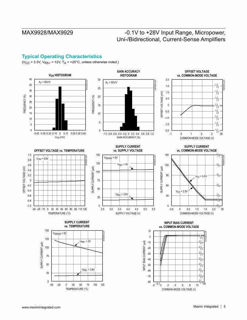
Typical Operating Characteristics

(VCC = 3.3V, VRS+ = 12V, TA = +25°C, unless otherwise noted.)
MAX9929FVOUT vs. VSENSE
MAX
9928
toc1
0
VSENSE (mV)
V OUT
(V)
12010080604020
1
2
3
4
5
6
00 140
VCC = 5.5V
VCC = 3.3V
VCC = 2.7VVCC = 2.5V
MAX9929FVOUT vs. VSENSE
MAX
9928
toc1
1
VSENSE (mV)
V OUT
(V)
8070605040
2.2
2.4
2.6
2.8
3.0
3.2
3.4
2.030 90
TA = -40°C
TA = +125°C
TA = +25°C
GAIN ACCURACYvs. SUPPLY VOLTAGE
MAX
9928
toc1
2
SUPPLY VOLTAGE (V)
GAIN
ACC
URAN
CY (%
)
5.04.54.03.53.0
-0.8
-0.6
-0.4
-0.2
0
0.2
0.4
0.6
0.8
1.0
-1.02.5 5.5
MINIMUM OUTPUT VOLTAGEvs. TEMPERATURE
MAX
9928
toc1
3
TEMPERATURE (°C)
MINI
MUM
OUTP
UT V
OLTA
GE (m
V)
1109565 80-10 5 20 35 50-25
0.5
1.0
1.5
2.0
2.5
3.0
3.5
4.0
4.5
5.0
0-40 125
GAIN ACCURACY vs. TEMPERATURE
MAX
9928
toc1
4
TEMPERATURE (°C)
GAIN
ACC
URAC
Y (%
)
1109565 80-10 5 20 35 50-25
-0.8
-0.6
-0.4
-0.2
0
0.2
0.4
0.6
0.8
1.0
-1.0-40 125
MAX9928FIOUT vs. VSENSE
MAX
9928
toc0
9
VSENSE (V)
I OUT
(µA)
0.40.30.20.1
500
1000
1500
2000
2500
00 0.5
TA = -40°C
TA = +125°C
VOUT = 0V
TA = +25°C
SMALL-SIGNAL GAINvs. FREQUENCY
MAX
9928
toc1
5
FREQUENCY (kHz)
GAIN
(dB)
1001010.1
23
26
29
32
35
200.01 1000
VCM = 3.6V
MAX992_F
CMRR vs. FREQUENCY
MAX
9928
toc1
6
FREQUENCY (Hz)
CMRR
(dB)
100k10k1k100
30
60
90
120
010 1M
MAX9928/MAX9929 -0.1V to +28V Input Range, Micropower, Uni-/Bidirectional, Current-Sense Amplifiers
Maxim Integrated 6www.maximintegrated.com
Typical Operating Characteristics (continued)
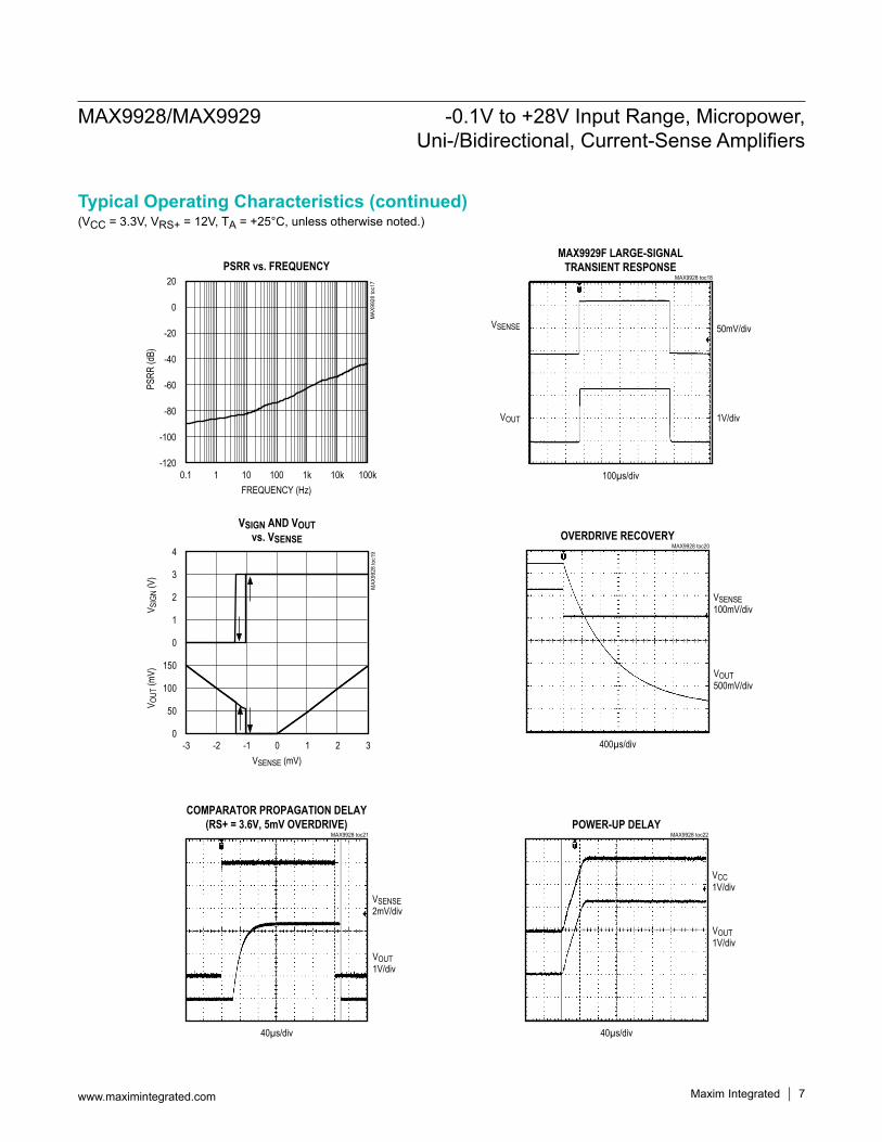
(VCC = 3.3V, VRS+ = 12V, TA = +25°C, unless otherwise noted.)
COMPARATOR PROPAGATION DELAY(RS+ = 3.6V, 5mV OVERDRIVE)
MAX9928 toc21
40µs/div
VSENSE2mV/div
VOUT1V/div
VSIGN AND VOUTvs. VSENSE
MAX
9928
toc1
9
VSENSE (mV)
V OUT
(mV)
V SIG
N (V
)
21-2 -1 0
50
100
150
0
1
2
3
4
0-3 3
PSRR vs. FREQUENCY
MAX
9928
toc1
7
FREQUENCY (Hz)
PSRR
(dB)
10k1k100101
-100
-80
-60
-40
-20
0
20
-1200.1 100k
POWER-UP DELAYMAX9928 toc22
40µs/div
VCC1V/div
VOUT1V/div
OVERDRIVE RECOVERYMAX9928 toc20
400µs/div
VSENSE100mV/div
VOUT500mV/div
MAX9929F LARGE-SIGNALTRANSIENT RESPONSE
MAX9928 toc18
100µs/div
VOUT
VSENSE
1V/div
50mV/div
MAX9928/MAX9929 -0.1V to +28V Input Range, Micropower, Uni-/Bidirectional, Current-Sense Amplifiers
Maxim Integrated 7www.maximintegrated.com
Typical Operating Characteristics (continued)
Detailed Description The MAX9928F/MAX9929F micropower uni-/bidirection-al, current-sense amplifiers feature -0.1V to +28V input common-mode range that is independent of the supply voltage. This wide input voltage range feature allows the monitoring of the current flow out of a power supply during short-circuit/fault conditions, and also enables highside current sensing at voltages far in excess of the supply voltage (VCC). The MAX9928F/MAX9929F operate from a 2.5V to 5.5V single supply and draw a low 20μA quies-cent supply current.Current flows through the sense resistor, generating a sense voltage VSENSE (Figure 1). The comparator sens-es the direction of the sense voltage and configures the amplifier for either positive or negative sense voltages by controlling the S1 and S2 switches.For positive VSENSE voltage, the amplifier’s inverting input is high impedance and equals VIN - VSENSE. The amplifier’s output drives the base of Q1, forcing its non-inverting input terminal to (VIN - VSENSE); this causes a current to flow through RG1 equal to |VSENSE|/RG1. Transistor Q2 and the current mirror amplify the current by a factor of M.For negative VSENSE voltage, the amplifier’s noninverting input is high impedance and the voltage on RS- terminal equals VIN + VSENSE. The amplifier’s output drives the base of Q1 forcing its inverting input terminal to match the voltage at the noninverting input terminal; this causes a current to flow through RG2 equal to |VSENSE|/RG2. Again, transistor Q2 and the current mirror amplify the current by a factor of M.
+VSENSE vs. -VSENSEThe amplifier is configured for either positive VSENSE or negative VSENSE by the SIGN comparator. The compara-tor has a built-in offset skew of -1.2mV so that random offsets in the comparator do not affect the precision of IOUT (VOUT) with positive VSENSE. The comparator has a small amount of hysteresis (typically 0.6mV) to prevent its output from oscillating at the crossover sense voltage. The ideal transfer characteristic of IOUT (VOUT) and the output of the comparator (SIGN) is shown in Figure 2.The amplifier VOS is only trimmed for the positive VSENSE voltages (VRS+ > VRS-). The SIGN comparator reconfigures the internal structure of the amplifier to work with negative VSENSE voltages (VRS- > VRS+) and the precision VOS trim is no longer effective and the result-ing VOS is slightly impacted. See details in the Electrical Characteristics Note 2. The user can choose the direction that needs the best precision to be the direction where VRS+ > VRS-. For example, when monitoring Li+ battery currents, the discharge current should be VRS+ > VRS- to give the best accuracy over the largest dynamic range. When the battery charger is plugged in, the charge cur-rent flows in the opposite direction and is usually much larger, and a higher VOS error can be tolerated. See the Typical Operating Circuit.For applications with unidirectional currents (e.g., battery discharge only), the SIGN output can be ignored.Note that as VSENSE increases, the output current (IOUT for the MAX9928 or VOUT/10kΩ for the MAX9929) also increases. This additional current is supplied from VCC.
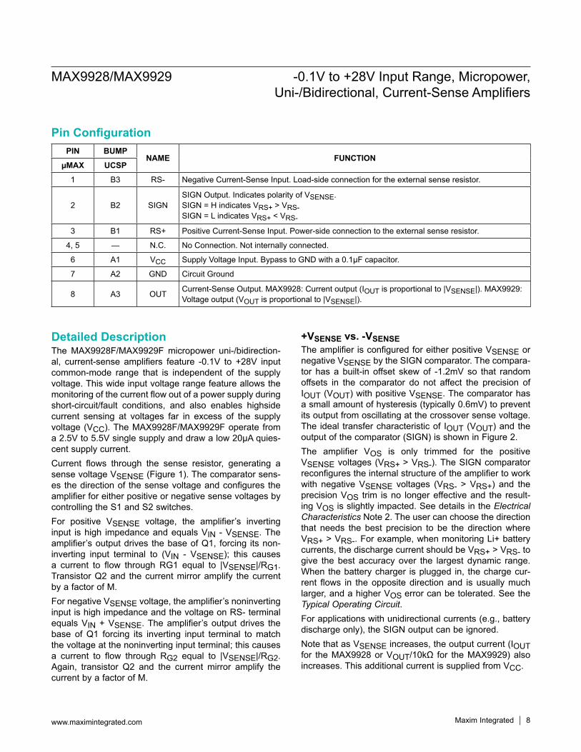
PIN BUMPNAME FUNCTION
µMAX UCSP
1 B3 RS- Negative Current-Sense Input. Load-side connection for the external sense resistor.
2 B2 SIGNSIGN Output. Indicates polarity of VSENSE.SIGN = H indicates VRS+ > VRS-SIGN = L indicates VRS+ < VRS-
3 B1 RS+ Positive Current-Sense Input. Power-side connection to the external sense resistor.
4, 5 — N.C. No Connection. Not internally connected.
6 A1 VCC Supply Voltage Input. Bypass to GND with a 0.1µF capacitor.
7 A2 GND Circuit Ground
8 A3 OUT Current-Sense Output. MAX9928: Current output (IOUT is proportional to |VSENSE|). MAX9929: Voltage output (VOUT is proportional to |VSENSE|).
MAX9928/MAX9929 -0.1V to +28V Input Range, Micropower, Uni-/Bidirectional, Current-Sense Amplifiers
www.maximintegrated.com Maxim Integrated 8
Pin Configuration

For both positive and negative VSENSE voltages, the cur-rent flowing out of the current mirror is equal to:
IOUT = M x |VSENSE|/RG1For the MAX9928F, the transconductance of the device is trimmed so that IOUT/|VSENSE| = 5μA/mV. For the MAX9929F, the voltage gain of the device is trimmed so that VOUT/|VSENSE| = 50V/V. The SIGN output from the comparator indicates the polarity of VSENSE.
Current Output (MAX9928F)The output voltage equation for the MAX9928_ is given below:
VOUT = (RSENSE x ILOAD) x (Gm X ROUT)where VOUT = the desired full-scale output voltage, ILOAD = the full-scale current being sensed, RSENSE = the current-sense resistor, ROUT = the voltage-setting resis-tor, and Gm = MAX9928F transconductance (5μA/mV).The full-scale output voltage range can be set by chang-ing the ROUT resistor value. The above equation can be modified to determine the ROUT required for a particular full-scale range:
ROUT = (VOUT)/(ILOAD x RSENSE x Gm)OUT is a high-impedance current source and can drive an unlimited amount of capacitance.Figure 2. Ideal Transfer Characteristics with 0mV Amplifier
Input Offset Voltage and -1mV Comparator Input Offset Voltage
Figure 1. Functional Diagram
0-1.2-1.8-3.0 3.02.01.0
0-1.2-1.8-3.0 3.02.01.0
VSENSE (mV)
VSENSE (mV)
SIGN
I OUT
(VOU
T)
( ) FOR THE MAX9929F.
CURRENTMIRROR
MAX9928FMAX9929F
C
S2
S1Q1
Q2 10kΩ*
SIGN
OUT
VCC
VIN-0.1V TO +28V
(VBATT)
R SEN
SE
V SEN
SE
+
-
2.5V TO 5.5V
RG180kΩ
RG280kΩ
RC280kΩ
RC180kΩ
RS-
RS+
TOLOAD/CHARGER
TO ADC
TO C
*INTERNAL 10kΩ RESISTOR FOR MAX9929_ ONLY.
GND
A
VCC
1MΩ
MAX9928/MAX9929 -0.1V to +28V Input Range, Micropower, Uni-/Bidirectional, Current-Sense Amplifiers
www.maximintegrated.com Maxim Integrated 9

Voltage Output (MAX9929F)The output voltage equation for the MAX9929_ is given below:
VOUT = (RSENSE x ILOAD) x (AV)where VOUT = the desired full-scale output voltage, ILOAD = the full-scale current being sensed, RSENSE = the current-sense resistor, AV = MAX9929F voltage gain (50V/V).
SIGN OutputThe current/voltage at OUT indicates magnitude. The SIGN output indicates the current’s direction. The SIGN comparator compares RS+ to RS-. The sign output is high when RS+ is greater than RS- indicating positive current flow. The sign output is low when RS- is greater than RS+ indicating negative current flow. In battery-operated sys-tems, this is useful for determining whether the battery is charging or discharging. The SIGN output might not cor-rectly indicate the direction of load current when VSENSE is between -1.8mV to -1.2mV (see Figure 2). Comparator hysteresis of 0.6mV prevents oscillation of SIGN output. If current direction is not needed, leave SIGN unconnected.
Applications InformationChoosing RSENSEThe MAX9928F/MAX9929F operate over a wide variety of current ranges with different sense resistors. Adjust the RSENSE value to monitor higher or lower current levels. Select RSENSE using these guidelines:
Voltage Loss: A high RSENSE value causes the power-source voltage to drop due to IR loss. For least voltage loss, use the lowest RSENSE value.
Accuracy: A high RSENSE value allows lower cur-rents to be measured more accurately. This is be-cause offsets become less significant when the sense voltage is larger.
Efficiency and Power Dissipation: At high current levels, the I2R losses in RSENSE might be significant. Take this into consideration when choosing the resis-
tor value and power dissipation (wattage) rating. Also, if the sense resistor is allowed to heat up excessively, its value could drift.
Inductance: If there is a large high-frequency compo-nent to ISENSE, keep inductance low. Wire-wound re-sistors have the highest inductance, while metal film is somewhat better. Low-inductance metal-film resis-tors are available. Instead of being spiral wrapped around a core, as in metal film or wirewound resistors, these are a straight band of metal. They are made in values under 1Ω.
Use in Systems with Super CapacitorsSince the input common-mode voltage range of the MAX9928/MAX9929 extends all the way from -0.1V to 28V, they are ideal to use in applications that require use of super capacitors for temporary or emergency energy storage systems. Some modern industrial systems use multifarad (1F–50F) capacitor banks to supply enough energy to keep critical systems alive even if the primary power source is removed or temporarily disabled. Unlike batteries, these capacitors can discharge all the way down to 0V. The MAX9928/MAX9929 can continuously help monitor their health and state of charge/discharge.
UCSP Applications InformationFor the latest application details on UCSP construc-tion, dimensions, tape carrier information, PCB tech-niques, bump-pad layout, and recommended reflow temperature profile, as well as the latest information on reliability testing results, go to Maxim’s website at www.maximintegrated.com/ucsp to find Application Note 1891: Wafer-Level Packaging (WLP) and its Applications.
Chip InformationPROCESS: BiCMOS
MAX9928/MAX9929 -0.1V to +28V Input Range, Micropower, Uni-/Bidirectional, Current-Sense Amplifiers
www.maximintegrated.com Maxim Integrated 10

1
2
3
4
8
7
6
5
OUT
GND
VCC
N.C.N.C.
RS+
SIGN
RS-
MAX9928FMAX9929F
µMAX
TOP VIEW
UCSP(1mm x 1.5mm)
TOP VIEW(BUMPS ON THE BOTTOM)
VCC GND OUT
1
A
B
2 3
RS+ SIGN RS-
MAX9928FMAX9929F
+
µC
DIGITALINPUT
ADC
GND
GND
RSENSE
2.5V TO5.5V0.1µF
VIN-0.1V TO
+28V
OUT
SIGNVCC
RS+ RS-
ROUT*
*FOR THE MAX9928F ONLY
MAX9928FMAX9929F
LOAD
WALL-CUBECHARGER
MAX9928/MAX9929 -0.1V to +28V Input Range, Micropower, Uni-/Bidirectional, Current-Sense Amplifiers
www.maximintegrated.com Maxim Integrated 11
Pin Configurations
Typical Operating Circuit
PACKAGE TYPE PACKAGE CODE OUTLINE NO. LAND PATTERN NO.
8 μMAX U8+1 21-0036 90-0092
6 UCSP B6+1 21-0097 —
MAX9928/MAX9929 -0.1V to +28V Input Range, Micropower, Uni-/Bidirectional, Current-Sense Amplifiers
www.maximintegrated.com Maxim Integrated 12
Package InformationFor the latest package outline information and land patterns (footprints), go to www.maximintegrated.com/packages. Note that a “+”, “#”, or “-” in the package code indicates RoHS status only. Package drawings may show a different suffix character, but the drawing pertains to the package regardless of RoHS status.

REVISIONNUMBER
REVISIONDATE DESCRIPTION PAGES
CHANGED
0 12/08 Initial release —
1 8/09 Removed MAX9928T and MAX9929T from data sheet 1–5, 7–12
2 4/11 Updated top marks 1
3 4/12 Removed the R61A1+1 package code note and references 1
4 9/14 Removed automotive reference from data sheet. 10
Maxim Integrated cannot assume responsibility for use of any circuitry other than circuitry entirely embodied in a Maxim Integrated product. No circuit patent licenses are implied. Maxim Integrated reserves the right to change the circuitry and specifications without notice at any time. The parametric values (min and max limits) shown in the Electrical Characteristics table are guaranteed. Other parametric values quoted in this data sheet are provided for guidance.
Maxim Integrated and the Maxim Integrated logo are trademarks of Maxim Integrated Products, Inc.
MAX9928/MAX9929 -0.1V to +28V Input Range, Micropower, Uni-/Bidirectional, Current-Sense Amplifiers
© 2014 Maxim Integrated Products, Inc. 13
Revision History
For pricing, delivery, and ordering information, please contact Maxim Direct at 1-888-629-4642, or visit Maxim Integrated’s website at www.maximintegrated.com.