Embed Size (px)
Citation preview
© Semiconductor Components Industries, LLC, 2016
June, 2016 − Rev. 41 Publication Order Number:
NCP715/D
NCP715
50 mA Ultra-Low Iq, WideInput Voltage, Low DropoutLinear Voltage Regulator
The NCP715 is 50 mA LDO Linear Voltage Regulator. It is a verystable and accurate device with ultra−low ground current consumption(4.7 �A over the full output load range) and a wide input voltage range(up to 24 V). The regulator incorporates several protection featuressuch as Thermal Shutdown and Current Limiting.
Features• Operating Input Voltage Range: 2.5 V to 24 V
• Fixed Voltage Options Available: 1.2 V to 5.3 V
• Ultra Low Quiescent Current: Max. 4.7 �A Over Full Load andTemperature
• ±2% Accuracy Over Full Load, Line and Temperature Variations
• PSRR: 52 dB at 100 kHz
• Noise: 190 �VRMS from 200 Hz to 100 kHz
• Thermal Shutdown and Current Limit protection
• Available in XDFN6 1.5 x 1.5 mm and SC−70 (SC−88A) Package
• These are Pb−Free Devices
Typical Applications• Portable Equipment
• Communication Systems
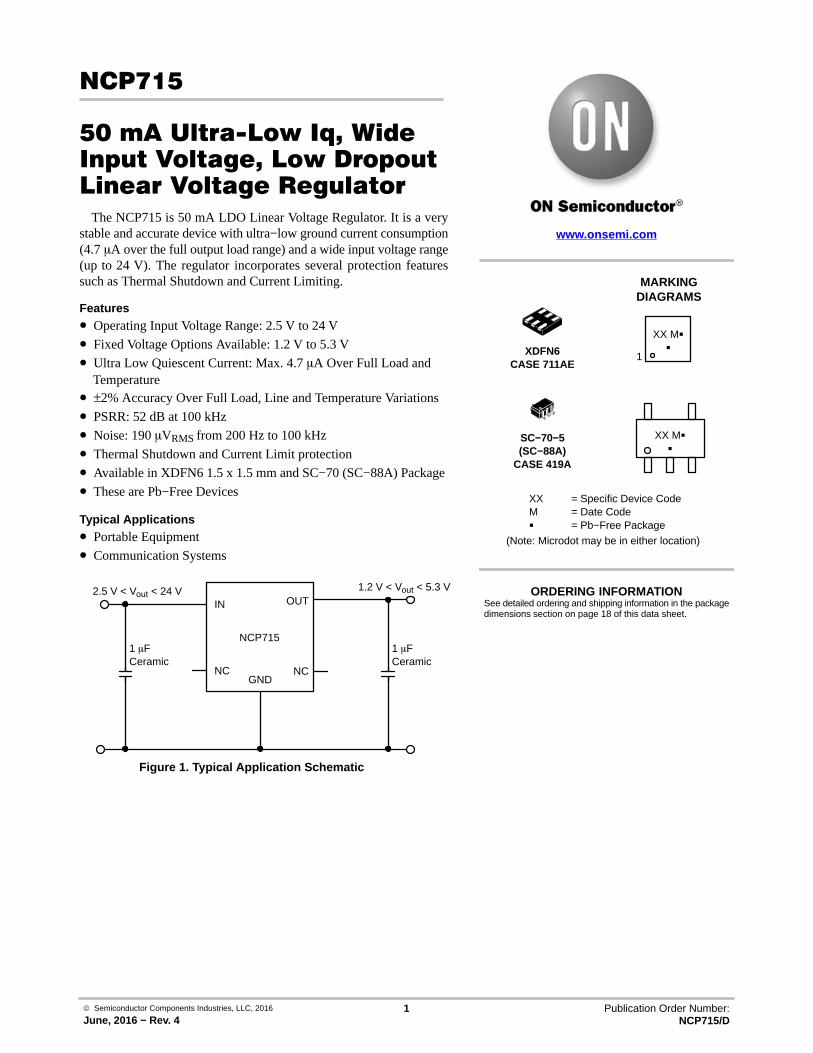
Figure 1. Typical Application Schematic
NCP715
NC
IN OUT
NCGND
1.2 V < Vout < 5.3 V2.5 V < Vout < 24 V
1 �FCeramic
1 �FCeramic
XDFN6CASE 711AE
MARKINGDIAGRAMS
www.onsemi.com
See detailed ordering and shipping information in the packagedimensions section on page 18 of this data sheet.
ORDERING INFORMATION
XX = Specific Device CodeM = Date Code� = Pb−Free Package
SC−70−5(SC−88A)
CASE 419A
XX M�
�
(Note: Microdot may be in either location)
XX M�
�
1

NCP715
www.onsemi.com2
IN
OUT
MOSFETDRIVER WITH
CURRENT LIMIT
THERMALSHUTDOWN
EEPROM
UVLO
GND
BANDGAPREFERENCE
Figure 2. Simplified Block Diagram
Figure 3. Pin Description
PIN FUNCTION DESCRIPTION
Pin No.
Pin Name DescriptionSC−70 XDFN6
5 6 OUT Regulated output voltage pin. A small 0.47 �F ceramic capacitor is needed from this pin toground to assure stability.
1 2 N/C No connection. This pin can be tied to ground to improve thermal dissipation or left disconnected.
2 3 GND Power supply ground.
3 4 N/C No connection. This pin can be tied to ground to improve thermal dissipation or left disconnected.
− 5 N/C No connection. This pin can be tied to ground to improve thermal dissipation or left disconnected.
4 1 IN Input pin. A small capacitor is needed from this pin to ground to assure stability.
NCP715
www.onsemi.com3
ABSOLUTE MAXIMUM RATINGS
Rating Symbol Value Unit
Input Voltage (Note 1) VIN −0.3 to 24 V
Output Voltage VOUT −0.3 to 6 V
Output Short Circuit Duration tSC Indefinite s
Maximum Junction Temperature TJ(MAX) 150 °C
Operating Ambient Temperature Range TA −40 to 125 °C
Storage Temperature Range TSTG −55 to 150 °C
ESD Capability, Human Body Model (Note 2) ESDHBM 2000 V
ESD Capability, Machine Model (Note 2) ESDMM 200 V
Stresses exceeding those listed in the Maximum Ratings table may damage the device. If any of these limits are exceeded, device functionalityshould not be assumed, damage may occur and reliability may be affected.1. Refer to ELECTRICAL CHARACTERISTICS and APPLICATION INFORMATION for Safe Operating Area.2. This device series incorporates ESD protection and is tested by the following methods:
ESD Human Body Model tested per EIA/JESD22−A114ESD Machine Model tested per EIA/JESD22−A115ESD Charged Device Model tested per EIA/JESD22−C101ELatch up Current Maximum Rating tested per JEDEC standard: JESD78.
THERMAL CHARACTERISTICS
Rating Symbol Value Unit
Thermal Characteristics, SC−70Thermal Resistance, Junction−to−Air
R�JA 390 °C/W
Thermal Characteristics, XDFN6Thermal Resistance, Junction−to−Air
R�JA 260 °C/W

NCP715
www.onsemi.com4
ELECTRICAL CHARACTERISTICS − Voltage Version 1.2 V−40°C ≤ TJ ≤ 125°C; VIN = 2.5 V; IOUT = 1 mA, CIN = COUT = 1.0 �F, unless otherwise noted. Typical values are at TJ = +25°C. (Note 5)
Parameter Test Conditions Symbol Min Typ Max Unit
Operating Input Voltage IOUT ≤ 10 mA VIN 2.5 24 V
10 mA< IOUT < 50 mA 3.0 24
Output Voltage Accuracy 2.5 V < VIN < 24 V, 0 < IOUT ≤ 10 mA VOUT 1.164 1.2 1.236 V
3.0 V < VIN < 24 V, 0 mA < IOUT < 50 mA VOUT 1.164 1.2 1.236 V
3.0 V < VIN < 24 V, 1 mA < IOUT < 50 mA,−20°C < TJ < 125°C;
VOUT 1.176 1.2 1.224 V
Line Regulation 2.5 V ≤ VIN ≤ 24 V, IOUT = 1 mA RegLINE 2 mV
Load Regulation IOUT = 0 mA to 50 mA RegLOAD 5 mV
Dropout Voltage (Note 3) VDO − mV
Maximum Output Current (Note 6) IOUT 100 200 mA
0 < IOUT < 50 mA, −40 < TA < 85°C IGND 3.2 4.2 �A
0 < IOUT < 50 mA, VIN = 24 V 5.8
Power Supply Rejection Ratio VIN = 3.0 V, VOUT = 1.2 VVPP = 200 mV modulationIOUT = 1 mA, COUT= 10 �F
f = 100 kHz PSRR 60 dB
Output Noise Voltage VOUT = 1.2 V, IOUT = 50 mAf = 200 Hz to 100 kHz, COUT = 10 �F
VN 65 �Vrms
Thermal Shutdown Temperature(Note 4)
Temperature increasing from TJ = +25°C TSD 170 °C
Thermal Shutdown Hysteresis (Note 4) Temperature falling from TSD TSDH − 15 − °C
3. Not Characterized at VIN = 3.0 V, VOUT = 1.2 V, IOUT = 50 mA.4. Guaranteed by design and characterization.5. Performance guaranteed over the indicated operating temperature range by design and/or characterization production tested at TJ = TA =
25°C. Low duty cycle pulse techniques are used during testing to maintain the junction temperature as close to ambient as possible.6. Respect SOA.

NCP715
www.onsemi.com5
ELECTRICAL CHARACTERISTICS − Voltage Version 1.5 V−40°C ≤ TJ ≤ 125°C; VIN = 2.5 V; IOUT = 1 mA, CIN = COUT = 1.0 �F, unless otherwise noted. Typical values are at TJ = +25°C. (Note 9)
Parameter Test Conditions Symbol Min Typ Max Unit
Operating Input Voltage IOUT ≤ 10 mA VIN 2.5 24 V
10 mA < IOUT < 50 mA 3.0 24
Output Voltage Accuracy 2.5 V < VIN < 24 V, 0 < IOUT ≤ 10 mA VOUT 1.455 1.5 1.545 V
3.0 V < VIN < 24 V, 0 < IOUT < 50 mA VOUT 1.455 1.5 1.545 V
3.0 V < VIN < 24 V, 1 mA < IOUT < 50 mA,−20°C < TJ < 125°C;
VOUT 1.470 1.5 1.530 V
Line Regulation VOUT + 1 V ≤ VIN ≤ 24 V, IOUT = 1 mA RegLINE 2 mV
Load Regulation IOUT = 0 mA to 50 mA RegLOAD 5 mV
Dropout Voltage (Note 7) VDO − mV
Maximum Output Current (Note 10) IOUT 100 200 mA
Ground Current 0 < IOUT < 50 mA, −40 < TA < 85°C IGND 3.2 4.2 �A
0 < IOUT < 50 mA, VIN = 24 V 5.8 �A
Power Supply Rejection Ratio VIN = 3.0 V, VOUT = 1.5 VVPP = 200 mV modulation
IOUT = 1 mA, COUT = 10 �F
f = 100 kHz PSRR 56 dB
Output Noise Voltage VOUT = 1.5 V, IOUT = 50 mAf = 200 Hz to 100 kHz, COUT = 10 �F
VN 75 �Vrms
Thermal Shutdown Temperature(Note 8)
Temperature increasing from TJ = +25°C TSD 170 °C
Thermal Shutdown Hysteresis (Note 8) Temperature falling from TSD TSDH − 15 − °C
7. Not Characterized at VIN = 3.0 V, VOUT = 1.5 V, IOUT = 50 mA.8. Guaranteed by design and characterization.9. Performance guaranteed over the indicated operating temperature range by design and/or characterization production tested at
TJ = TA = 25°C. Low duty cycle pulse techniques are used during testing to maintain the junction temperature as close to ambient as possible.10.Respect SOA.
NCP715
www.onsemi.com6
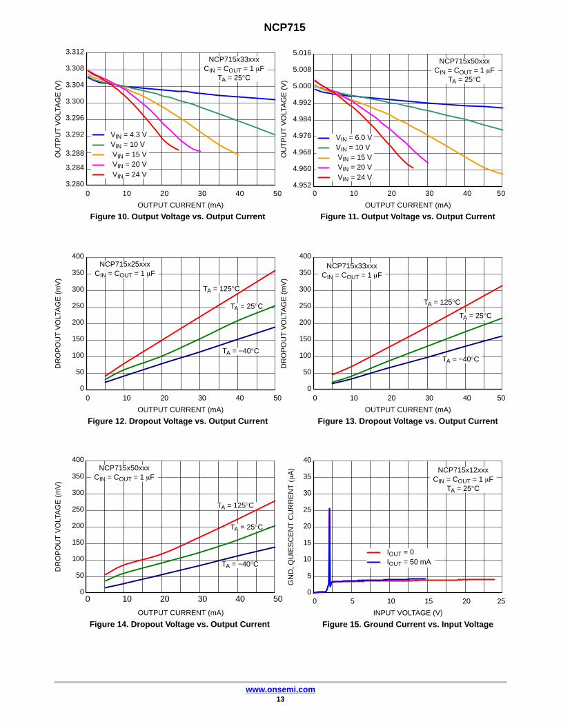
ELECTRICAL CHARACTERISTICS − Voltage Version 1.8 V−40°C ≤ TJ ≤ 125°C; VIN = 2.8V; IOUT = 1 mA, CIN = COUT = 1.0 �F, unless otherwise noted. Typical values are at TJ = +25°C. (Note 13)
Parameter Test Conditions Symbol Min Typ Max Unit
Operating Input Voltage IOUT ≤10 mA VIN 2.8 24 V
10 mA < IOUT < 50 mA 3.0 24
Output Voltage Accuracy 2.8 V < VIN < 24 V, 0 < IOUT < 10 mA VOUT 1.746 1.8 1.854 V
3.0 V < VIN < 24 V, 1 mA < IOUT < 50 mA,−20°C < TJ < 125°C;
VOUT 1.764 1.8 1.836 V
Line Regulation 3 V ≤ VIN ≤ 24 V, IOUT = 1 mA RegLINE 3 mV
Load Regulation IOUT = 0 mA to 50 mA RegLOAD 10 mV
Dropout Voltage (Note 11) VDO mV
Maximum Output Current (Note 14) IOUT 100 200 mA
Ground Current 0 < IOUT < 50 mA, −40 < TA < 85°C IGND 3.2 4.2 �A
0 < IOUT < 50 mA, VIN = 24 V 5.8 �A
Power Supply Rejection Ratio VIN = 3.0 V, VOUT = 1.8 VVPP = 200 mV modulationIOUT = 1 mA, COUT =10 �F
f = 100 kHz PSRR 60 dB
Output Noise Voltage VOUT = 1.8 V, IOUT = 50 mAf = 200 Hz to 100 kHz, COUT = 10 �F
VN 95 �Vrms
Thermal Shutdown Temperature(Note 12)
Temperature increasing from TJ = +25°C TSD 170 °C
Thermal Shutdown Hysteresis(Note 12)
Temperature falling from TSD TSDH − 15 − °C
11. Not characterized at VIN = 3.0 V, VOUT = 1.8 V, IOUT = 50 mA12.Guaranteed by design and characterization.13.Performance guaranteed over the indicated operating temperature range by design and/or characterization production tested at TJ = TA =
25°C. Low duty cycle pulse techniques are used during testing to maintain the junction temperature as close to ambient as possible.14.Respect SOA.

NCP715
www.onsemi.com7
ELECTRICAL CHARACTERISTICS − Voltage Version 2.5 V−40°C ≤ TJ ≤ 125°C; VIN = 3.5 V; IOUT = 1 mA, CIN = COUT = 1.0 �F, unless otherwise noted. Typical values are at TJ = +25°C. (Note 17)
Parameter Test Conditions Symbol Min Typ Max Unit
Operating Input Voltage 0 < IOUT < 50 mA VIN 3.5 24 V
Output Voltage Accuracy 3.5 V < VIN < 24 V, 0 < IOUT < 50 mA VOUT 2.45 2.5 2.55 V
Line Regulation VOUT + 1 V ≤ VIN ≤ 24 V, IOUT = 1 mA RegLINE 3 mV
Load Regulation IOUT = 0 mA to 50 mA RegLOAD 10 mV
Dropout Voltage (Note 15) VDO = VIN – (VOUT(NOM) – 75 mV)IOUT = 50 mA
VDO 260 450 mV
Maximum Output Current (Note 18) IOUT 100 200 mA
Ground Current0 < IOUT < 50 mA, −40 < TA < 85°C IGND 3.2 4.2 �A
0 < IOUT < 50 mA, VIN = 24 V 5.8 �A
Power Supply Rejection Ratio VIN = 3.5 V, VOUT = 2.5 VVPP = 200 mV modulationIOUT = 1 mA, COUT =10 �F
f = 100 kHz PSRR 60 dB
Output Noise Voltage VOUT = 2.5 V, IOUT = 50 mAf = 200 Hz to 100 kHz, COUT = 10 �F
VN 115 �Vrms
Thermal Shutdown Temperature(Note 16)
Temperature increasing from TJ = +25°C TSD 170 °C
Thermal Shutdown Hysteresis(Note 16)
Temperature falling from TSD TSDH − 15 − °C
15.Characterized when VOUT falls 75 mV below the regulated voltage and only for devices with VOUT = 2.5 V.16.Guaranteed by design and characterization.17.Performance guaranteed over the indicated operating temperature range by design and/or characterization production tested at
TJ = TA = 25°C. Low duty cycle pulse techniques are used during testing to maintain the junction temperature as close to ambient as possible.18.Respect SOA.

NCP715
www.onsemi.com8
ELECTRICAL CHARACTERISTICS − Voltage Version 3.0 V−40°C ≤ TJ ≤ 125°C; VIN = 4.0 V; IOUT = 1 mA, CIN = COUT = 1.0 �F, unless otherwise noted. Typical values are at TJ = +25°C. (Note 21)
Parameter Test Conditions Symbol Min Typ Max Unit
Operating Input Voltage 0 < IOUT < 50 mA VIN 4.0 24 V
Output Voltage Accuracy 4.0 V < VIN < 24 V, 0< IOUT < 50 mA VOUT 2.94 3.0 3.06 V
Line Regulation VOUT + 1 V ≤ VIN ≤ 24 V, IOUT = 1 mA RegLINE 3 mV
Load Regulation IOUT = 0 mA to 50 mA RegLOAD 10 mV
Dropout voltage (Note 19) VDO = VIN – (VOUT(NOM) – 90 mV)IOUT = 50 mA
VDO
250400 mV
Maximum Output Current (Note 22) IOUT 100 200 mA
Ground current 0 < IOUT < 50 mA, -40 < TA < 85°C IGND 3.2 4.2 �A
0 < IOUT < 50 mA, VIN = 24 V 5.8 �A
Power Supply Rejection Ratio VIN = 4.0 V, VOUT = 3.0 VVPP = 100 mV modulation
IOUT = 1 mA, COUT = 10 �F
f = 100 kHz PSRR 60 dB
Output Noise Voltage VOUT = 3 V, IOUT = 50 mA,f = 200 Hz to 100 kHz, COUT = 10 �F
VN 135 �Vrms
Thermal Shutdown Temperature(Note 20)
Temperature increasing from TJ = +25°C TSD 170 °C
Thermal Shutdown Hysteresis (Note 20)
Temperature falling from TSD TSDH - 25 - °C
19.Characterized when VOUT falls 90 mV below the regulated voltage and only for devices with VOUT = 3.0 V20.Guaranteed by design and characterization.21.Performance guaranteed over the indicated operating temperature range by design and/or characterization production tested
at TJ = TA = 25°C. Low duty cycle pulse techniques are used during testing to maintain the junction temperature as close to ambient aspossible.
22.Respect SOA

NCP715
www.onsemi.com9
ELECTRICAL CHARACTERISTICS − Voltage Version 3.3 V−40°C ≤ TJ ≤ 125°C; VIN = 4.3 V; IOUT = 1 mA, CIN = COUT = 1.0 �F, unless otherwise noted. Typical values are at TJ = +25°C. (Note 25)
Parameter Test Conditions Symbol Min Typ Max Unit
Operating Input Voltage 0 < IOUT < 50 mA VIN 4.3 24 V
Output Voltage Accuracy 4.3 V < VIN < 24 V, 0 < IOUT < 50 mA VOUT 3.234 3.3 3.366 V
Line Regulation VOUT + 1 V ≤ VIN ≤ 24 V, IOUT = 1 mA RegLINE 3 10 mV
Load Regulation IOUT = 0 mA to 50 mA RegLOAD 10 mV
Dropout Voltage (Note 23) VDO = VIN – (VOUT(NOM) – 99 mV)IOUT = 50 mA
VDO 230 350 mV
Maximum Output Current (Note 26) IOUT 100 200 mA
Ground Current 0 < IOUT < 50 mA, −40 < TA < 85°C IGND 3.2 4.2 �A
0 < IOUT < 50 mA, VIN = 24 V 5.8 �A
Power Supply Rejection Ratio VIN = 4.3 V, VOUT = 3.3 VVPP = 200 mV modulationIOUT = 1 mA, COUT =10 �F
f = 100 kHz PSRR 60 dB
Output Noise Voltage VOUT = 4.3 V, IOUT = 50 mAf = 200 Hz to 100 kHz, COUT = 10 �F
VN 140 �Vrms
Thermal Shutdown Temperature(Note 24)
Temperature increasing from TJ = +25°C TSD 170 °C
Thermal Shutdown Hysteresis(Note 24)
Temperature falling from TSD TSDH − 15 − °C
23.Characterized when VOUT falls 99 mV below the regulated voltage and only for devices with VOUT = 3.3 V.24.Guaranteed by design and characterization.25.Performance guaranteed over the indicated operating temperature range by design and/or characterization production tested at TJ = TA =
25°C. Low duty cycle pulse techniques are used during testing to maintain the junction temperature as close to ambient as possible.26.Respect SOA.

NCP715
www.onsemi.com10
ELECTRICAL CHARACTERISTICS − Voltage Version 5.0 V−40°C ≤ TJ ≤ 125°C; VIN = 6.0 V; IOUT = 1 mA, CIN = COUT = 1 �F, unless otherwise noted. Typical values are at TJ = +25°C. (Note 29)
Parameter Test Conditions Symbol Min Typ Max Unit
Operating Input Voltage 0 < IOUT < 50 mA VIN 6.0 24 V
Output Voltage Accuracy 6.0V < VIN < 24V, 0< IOUT < 50 mA VOUT 4.9 5.0 5.1 V
Line Regulation VOUT + 1 V ≤ VIN ≤ 24 V, Iout = 1mA RegLINE 3 10 mV
Load Regulation IOUT = 0 mA to 50 mA RegLOAD 10 30 mV
Dropout Voltage (Note 27) VDO = VIN – (VOUT(NOM) – 150 mV)IOUT = 50 mA
VDO 230 350 mV
Maximum Output Current (Note 30) IOUT 90 200 mA
Ground Current 0 < IOUT < 50 mA, −40 < TA < 85°C IGND 3.2 4.2 �A
0 < IOUT < 50 mA, VIN = 24 V 5.8 �A
Power Supply Rejection Ratio VIN = 6.0 V, VOUT = 5.0 VVPP = 200 mV modulationIOUT = 1 mA, COUT =10 �F
f = 100 kHz PSRR 56 dB
Output Noise Voltage VOUT = 5.0 V, IOUT = 50 mAf = 200 Hz to 100 kHz, COUT = 10 �F
VN 190 �Vrms
Thermal Shutdown Temperature(Note 28)
Temperature increasing from TJ = +25°C TSD 170 °C
Thermal Shutdown Hysteresis(Note 28)
Temperature falling from TSD TSDH − 15 − °C
27.Characterized when VOUT falls 150 mV below the regulated voltage and only for devices with VOUT = 5.0 V.28.Guaranteed by design and characterization.29.Performance guaranteed over the indicated operating temperature range by design and/or characterization production tested at TJ = TA =
25°C. Low duty cycle pulse techniques are used during testing to maintain the junction temperature as close to ambient as possible.30.Respect SOA.

NCP715
www.onsemi.com11
ELECTRICAL CHARACTERISTICS − Voltage Version 5.3 V−40°C ≤ TJ ≤ 125°C; VIN = 6.3 V; IOUT = 1 mA, CIN = COUT = 1 �F, unless otherwise noted. Typical values are at TJ = +25°C. (Note 33)
Parameter Test Conditions Symbol Min Typ Max Unit
Operating Input Voltage 0 < IOUT < 50 mA VIN 6.3 24 V
Output Voltage Accuracy 6.3V < VIN < 24V, 0.1 mA< IOUT < 50 mA VOUT 5.194 5.3 5.406 V
Line Regulation VOUT + 1 V ≤ VIN ≤ 24 V, IOUT = 1mA RegLINE 20 60 mV
Load Regulation IOUT = 0.1 mA to 50 mA RegLOAD 20 mV
Dropout Voltage (Note 31) VDO = VIN – (VOUT(NOM) – 159 mV)IOUT = 50 mA
VDO 230 350 mV
Maximum Output Current (Note 34) IOUT 90 200 mA
Ground Current 0 < IOUT < 50 mA, −40 < TA < 85°C IGND 3.2 4.2 �A
0 < IOUT < 50 mA, VIN = 24 V 5.8 �A
Power Supply Rejection Ratio VIN = 6.3 V, VOUT = 5.3 VVPP = 200 mV modulationIOUT = 1 mA, COUT =10 �F
f = 100 kHz PSRR 55 dB
Output Noise Voltage VOUT = 5.3 V, IOUT = 50 mAf = 200 Hz to 100 kHz, COUT = 10 �F
VN 195 �Vrms
Thermal Shutdown Temperature(Note 32)
Temperature increasing from TJ = +25°C TSD 170 °C
Thermal Shutdown Hysteresis(Note 32)
Temperature falling from TSD TSDH − 15 − °C
31.Characterized when VOUT falls 159 mV below the regulated voltage and only for devices with VOUT = 5.3 V.32.Guaranteed by design and characterization.33.Performance guaranteed over the indicated operating temperature range by design and/or characterization production tested at TJ = TA =
25°C. Low duty cycle pulse techniques are used during testing to maintain the junction temperature as close to ambient as possible.34.Respect SOA.

NCP715
www.onsemi.com12
2.472
2.476
2.480
2.484
2.488
2.492
2.496
2.500
2.504
0 10 20 30 40 501.172
1.176
1.180
1.184
1.188
1.192
1.196
1.200
1.204
0 10 20 30 40 50
VIN = 3.5 VVIN = 5.0 VVIN = 10 VVIN = 15 VVIN = 20 VVIN = 24 V
4.98
4.985
4.99
4.995
5
5.005
5.01
5.015
5.02
−40 −20 0 20 40 60 80 100 120
Figure 4. Output Voltage vs. Temperature Figure 5. Output Voltage vs. Temperature
Figure 6. Output Voltage vs. Temperature Figure 7. Output Voltage vs. Temperature
Figure 8. Output Voltage vs. Output Current Figure 9. Output Voltage vs. Output Current
1.2
−40 −20 0 12010020 40 60 80
TEMPERATURE (°C)
OU
TP
UT
VO
LTA
GE
(V
)VIN = 3.0 V
NCP715x12xxxCIN = COUT = 1 �F
IOUT = 1 mA
TEMPERATURE (°C)
OU
TP
UT
VO
LTA
GE
(V
)
2.506
−40 −20 0 12010020 40 60 80
3.318
−40 −20 0 12010020 40 60 80TEMPERATURE (°C)
OU
TP
UT
VO
LTA
GE
(V
)
JUNCTION TEMPERATURE (°C)
OU
TP
UT
VO
LTA
GE
(V
)
OUTPUT CURRENT (mA)
OU
TP
UT
VO
LTA
GE
(V
)
OUTPUT CURRENT (mA)
OU
TP
UT
VO
LTA
GE
(V
)
VIN = (5.0 − 24.0) V
1.199
1.198
1.197
1.196
1.195
1.194
1.193
1.192
VIN = 3.0 V
VIN = (5.0 − 24.0) V
2.504
2.502
2.5
2.498
2.496
2.494
2.492
2.49
NCP715x25xxxCIN = COUT = 1 �F
IOUT = 1 mA
3.315
3.312
3.309
3.306
3.303
3.3
3.297
3.294
NCP715x33xxxCIN = COUT = 1 �F
IOUT = 1 mAVIN = 4.3 V to 24 V
NCP715x50xxxCIN = COUT = 1 �F
IOUT = 1 mA
VIN = 6.0 V
VIN = (8.0 − 24.0) V
NCP715x12xxxCIN = COUT = 1 �F
TA = 25°C
VIN = 3.0 VVIN = 5.0 VVIN = 10 VVIN = 15 VVIN = 20 VVIN = 24 V
NCP715x25xxxCIN = COUT = 1 �F
TA = 25°C
NCP715
www.onsemi.com13
4.952
4.960
4.968
4.976
4.984
4.992
5.000
5.008
5.016
0 10 20 30 40 50
Figure 10. Output Voltage vs. Output Current Figure 11. Output Voltage vs. Output CurrentOUTPUT CURRENT (mA)
OU
TP
UT
VO
LTA
GE
(V
)
OUTPUT CURRENT (mA)
OU
TP
UT
VO
LTA
GE
(V
)
3.280
3.284
3.288
3.292
3.296
3.300
3.304
3.308
3.312
0 10 20 30 40 50
VIN = 4.3 V
VIN = 15 VVIN = 20 VVIN = 24 V
NCP715x33xxxCIN = COUT = 1 �F
TA = 25°C
VIN = 10 VVIN = 6.0 V
VIN = 15 VVIN = 20 VVIN = 24 V
VIN = 10 V
NCP715x50xxxCIN = COUT = 1 �F
TA = 25°C
0
50
100
150
200
250
300
350
400
0 10 20 30 40 50
Figure 12. Dropout Voltage vs. Output CurrentOUTPUT CURRENT (mA)
DR
OP
OU
T V
OLT
AG
E (
mV
)
TA = 125°C
TA = 25°C
TA = −40°C
NCP715x25xxxCIN = COUT = 1 �F
0
50
100
150
200
250
300
350
400
0 10 20 30 40 50
Figure 13. Dropout Voltage vs. Output CurrentOUTPUT CURRENT (mA)
DR
OP
OU
T V
OLT
AG
E (
mV
)
NCP715x33xxxCIN = COUT = 1 �F
TA = 125°C
TA = 25°C
TA = −40°C
0
50
100
150
200
250
300
350
400
0 10 20 30 40 50
Figure 14. Dropout Voltage vs. Output CurrentOUTPUT CURRENT (mA)
DR
OP
OU
T V
OLT
AG
E (
mV
)
TA = 125°C
TA = 25°C
TA = −40°C
NCP715x50xxxCIN = COUT = 1 �F
0
5
10
15
20
25
30
35
40
0 5 10 15 20 25
IOUT = 0IOUT = 50 mA
Figure 15. Ground Current vs. Input VoltageINPUT VOLTAGE (V)
GN
D, Q
UIE
SC
EN
T C
UR
RE
NT
��A
) NCP715x12xxxCIN = COUT = 1 �F
TA = 25°C
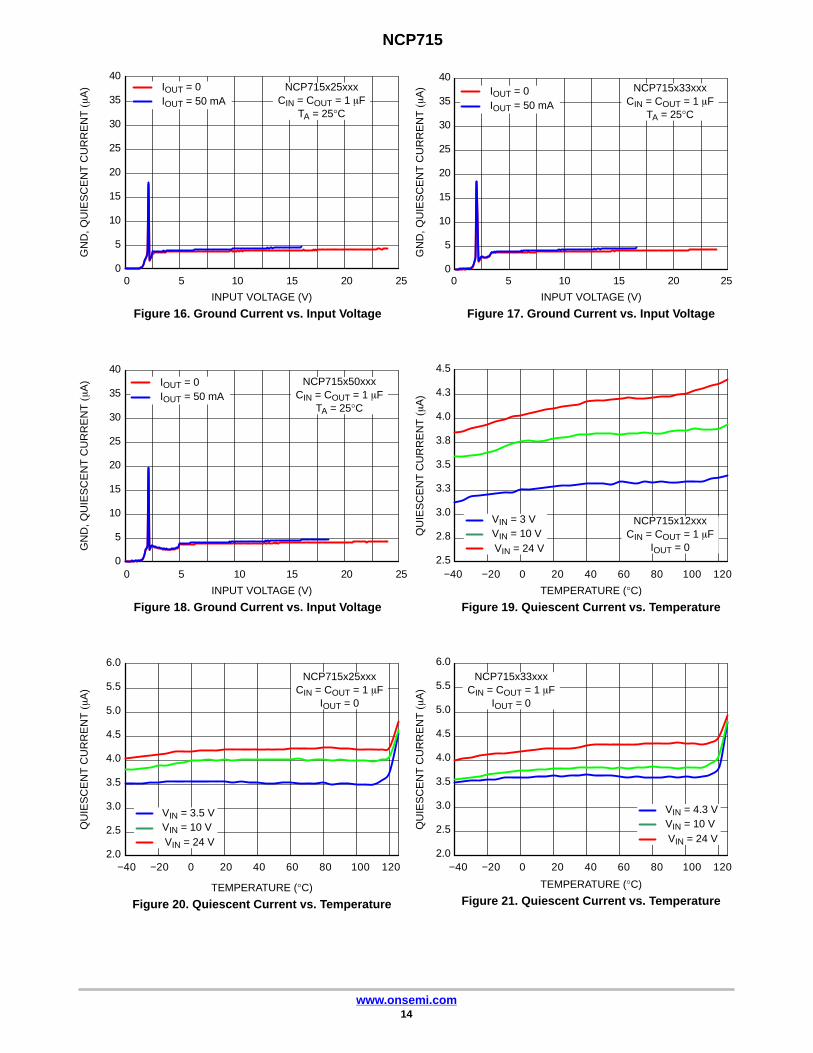
NCP715
www.onsemi.com14
0
5
10
15
20
25
30
35
40
0 5 10 15 20 25
Figure 16. Ground Current vs. Input Voltage Figure 17. Ground Current vs. Input VoltageINPUT VOLTAGE (V)
GN
D, Q
UIE
SC
EN
T C
UR
RE
NT
��A
)
INPUT VOLTAGE (V)
GN
D, Q
UIE
SC
EN
T C
UR
RE
NT
��A
)
0
5
10
15
20
25
30
35
40
0 5 10 15 20 25
IOUT = 0IOUT = 50 mA
NCP715x25xxxCIN = COUT = 1 �F
TA = 25°C
IOUT = 0IOUT = 50 mA
NCP715x33xxxCIN = COUT = 1 �F
TA = 25°C
0
5
10
15
20
25
30
35
40
0 5 10 15 20 25
Figure 18. Ground Current vs. Input VoltageINPUT VOLTAGE (V)
GN
D, Q
UIE
SC
EN
T C
UR
RE
NT
��A
) IOUT = 0IOUT = 50 mA
NCP715x50xxxCIN = COUT = 1 �F
TA = 25°C
2.5
2.8
3.0
3.3
3.5
3.8
4.0
4.3
4.5
−40 −20 0 20 40 60 80 100 120
Figure 19. Quiescent Current vs. TemperatureTEMPERATURE (°C)
QU
IES
CE
NT
CU
RR
EN
T ��A
)
VIN = 3 V
VIN = 24 V
NCP715x12xxxCIN = COUT = 1 �F
IOUT = 0VIN = 10 V
2.0
2.5
3.0
3.5
4.0
4.5
5.0
5.5
6.0
Figure 20. Quiescent Current vs. TemperatureTEMPERATURE (°C)
QU
IES
CE
NT
CU
RR
EN
T ��A
)
−40 −20 0 20 40 60 80 100 120
VIN = 3.5 V
VIN = 24 V
NCP715x25xxxCIN = COUT = 1 �F
IOUT = 0
VIN = 10 V
2.0
2.5
3.0
3.5
4.0
4.5
5.0
5.5
6.0
Figure 21. Quiescent Current vs. TemperatureTEMPERATURE (°C)
QU
IES
CE
NT
CU
RR
EN
T ��A
)
−40 −20 0 20 40 60 80 100 120
VIN = 4.3 V
VIN = 24 V
NCP715x33xxxCIN = COUT = 1 �F
IOUT = 0
VIN = 10 V

NCP715
www.onsemi.com15
2.0
2.5
3.0
3.5
4.0
4.5
5.0
5.5
6.0
Figure 22. Quiescent Current vs. TemperatureTEMPERATURE (°C)
QU
IES
CE
NT
CU
RR
EN
T ��A
)
−40 −20 0 20 40 60 80 100 120
VIN = 6 V
VIN = 24 V
NCP715x50xxxCIN = COUT = 1 �F
IOUT = 0
VIN = 10 V
Figure 23. PSRR vs. FrequencyFREQUENCY (kHz)
PS
RR
(dB
)
0
20
40
60
80
100
0.1 1 10 100 1000
NCP715x12xxxCOUT = 10 �FVIN = 3.0 V + 200 mVPP ModulationTA = 25°C
IOUT = 1 mA
IOUT = 10 mAIOUT = 50 mA
0
20
40
60
80
100
0.1 1 10 100 1000
Figure 24. PSRR vs. FrequencyFREQUENCY (kHz)
PS
RR
(dB
)
IOUT = 1 mA
IOUT = 10 mAIOUT = 50 mA
NCP715x25xxxCOUT = 10 �FVIN = 3.5 V + 200 mVPP ModulationTA = 25°C
0
20
40
60
80
100
0.1 1 10 100 1000
PS
RR
(dB
)
Figure 25. PSRR vs. FrequencyFREQUENCY (kHz)
IOUT = 1 mA
IOUT = 10 mA
IOUT = 50 mA
NCP715x33xxxCOUT = 10 �FVIN = 4.3 V + 200 mVPP ModulationTA = 25°C
0
20
40
60
80
100
0.1 1 10 100 1000
Figure 26. PSRR vs. FrequencyFREQUENCY (kHz)
PS
RR
(dB
)
NCP715x50xxxCOUT = 10 �FVIN = 6.0 V + 200 mVPP ModulationTA = 25°C
IOUT = 1 mA
IOUT = 10 mAIOUT = 50 mA
0.0
0.2
0.4
0.6
0.8
1.0
1.2
1.4
1.6
0.01 0.1 1 10 100 1000
OU
TP
UT
VO
LTA
GE
NO
ISE
(�V
/√H
z)
Figure 27. Output Spectral Noise Density vs.Frequency
FREQUENCY (kHz)
COUT = 10 �F, 65.1 �Vrms @ 200 Hz − 100 kHz
COUT = 2.2 �F, 111.5 �Vrms @ 200 Hz − 100 kHz
COUT = 1.0 �F, 172.1 �Vrms @ 200 Hz − 100 kHz
COUT = 0.47 �F, 208 �Vrms @ 200 Hz − 100 kHz
COUT = 4.7 �F, 80.5 �Vrms @ 200 Hz − 100 kHz
NCP715x12xxxIOUT = 50 mA
TA = 25°CVIN = 3 V

NCP715
www.onsemi.com16
0.0
0.5
1.0
1.5
2.0
2.5
3.0
3.5
4.0
0.01 0.1 1 10 100 1000
OU
TP
UT
VO
LTA
GE
NO
ISE
(�V
/√H
z)
Figure 28. Output Spectral Noise Density vs.Frequency
FREQUENCY (kHz)
COUT = 10 �F, 114.7 �Vrms @ 200 Hz − 100 kHz
COUT = 2.2 �F, 152.2 �Vrms @ 200 Hz − 100 kHz
COUT = 1.0 �F, 172.1 �Vrms @ 200 Hz − 100 kHz
COUT = 0.47 �F, 203.6 �Vrms @ 200 Hz − 100 kHz
COUT = 4.7 �F, 128.4 �Vrms @ 200 Hz − 100 kHz
NCP715x25xxxIOUT = 50 mA
TA = 25°CVIN = 3.5 V
0.0
0.5
1.0
1.5
2.0
2.5
3.0
3.5
4.0
4.5
5.0
0.01 0.1 1 10 100 1000
OU
TP
UT
VO
LTA
GE
NO
ISE
(�V
/√H
z)
Figure 29. Output Spectral Noise Density vs.Frequency
FREQUENCY (kHz)
COUT = 10 �F, 137.1 �Vrms @ 200 Hz − 100 kHz
COUT = 2.2 �F, 170.6 �Vrms @ 200 Hz − 100 kHz
COUT = 1.0 �F, 220.8 �Vrms @ 200 Hz − 100 kHz
COUT = 0.47 �F, 271.1 �Vrms @ 200 Hz − 100 kHz
COUT = 4.7 �F, 145.7 �Vrms @ 200 Hz − 100 kHz
NCP715x33xxxIOUT = 50 mA
TA = 25°CVIN = 4.3 V
0.0
1.0
2.0
3.0
4.0
5.0
6.0
7.0
0.01 0.1 1 10 100 1000
OU
TP
UT
VO
LTA
GE
NO
ISE
(�V
/√H
z)
Figure 30. Output Spectral Noise Density vs.Frequency
FREQUENCY (kHz)
COUT = 10 �F, 186.1 �Vrms @ 200 Hz − 100 kHz
COUT = 2.2 �F, 207.6 �Vrms @ 200 Hz − 100 kHz
COUT = 1.0 �F, 244.5 �Vrms @ 200 Hz − 100 kHz
COUT = 0.47 �F, 305.0 �Vrms @ 200 Hz − 100 kHz
COUT = 4.7 �F, 189.41 �Vrms @ 200 Hz − 100 kHz
NCP715x50xxxIOUT = 50 mA
TA = 25°CVIN = 6.0 V
Figure 31. Line Transient Response
Figure 32. Line Transient Response Figure 33. Line Transient Response

NCP715
www.onsemi.com17
Figure 34. Load Transient Response Figure 35. Load Transient Response
Figure 36. Load Transient Response Figure 37. Input Voltage Turn−On Response
Figure 38. Input Voltage Turn−On Response Figure 39. Input Voltage Turn−On Response

NCP715
www.onsemi.com18
APPLICATIONS INFORMATION
The NCP715 is the member of new family of Wide InputVoltage Range Low Dropout Regulators which deliversUltra Low Ground Current consumption, Good Noise andPower Supply Rejection Ratio Performance.
Input Decoupling (CIN)It is recommended to connect at least 0.1 �F Ceramic X5R
or X7R capacitor between IN and GND pin of the device.This capacitor will provide a low impedance path for anyunwanted AC signals or Noise superimposed onto constantInput Voltage. The good input capacitor will limit theinfluence of input trace inductances and source resistanceduring sudden load current changes.
Higher capacitance and lower ESR Capacitors willimprove the overall line transient response.
Output Decoupling (COUT)The NCP715 does not require a minimum Equivalent
Series Resistance (ESR) for the output capacitor. The deviceis designed to be stable with standard ceramics capacitorswith values of 0.47 �F or greater up to 10 �F. The X5R andX7R types have the lowest capacitance variations overtemperature thus they are recommended.
Power Dissipation and Heat sinkingThe maximum power dissipation supported by the device
is dependent upon board design and layout. Mounting padconfiguration on the PCB, the board material, and the
ambient temperature affect the rate of junction temperaturerise for the part. The maximum power dissipation theNCP715 can handle is given by:
PD(MAX) ��TJ(MAX) � TA
�R�JA
(eq. 1)
The power dissipated by the NCP715 for givenapplication conditions can be calculated from the followingequations:
PD � VIN�IGND
�IOUT�� IOUT
�VIN � VOUT� (eq. 2)
or
VIN(MAX) �PD(MAX) �VOUT IOUT
�
IOUT IGND
(eq. 3)
For reliable operation, junction temperature should belimited to +125°C maximum.
HintsVIN and GND printed circuit board traces should be as
wide as possible. When the impedance of these traces ishigh, there is a chance to pick up noise or cause the regulatorto malfunction. Place external components, especially theoutput capacitor, as close as possible to the NCP715, andmake traces as short as possible.
ORDERING INFORMATION
Device Nominal Output Voltage Marking Marking Rotation Package Shipping†
NCP715SQ12T2G 1.2 V 5A
−SC88A/SC70
(Pb−Free)
3000 / Tape& Reel
NCP715SQ15T2G 1.5 V 5C
NCP715SQ18T2G 1.8 V 5D
NCP715SQ25T2G 2.5 V 5E
NCP715SQ30T2G 3.0 V 5F
NCP715SQ33T2G 3.3 V 5G
NCP715SQ50T2G 5.0 V 5H
NCP715MX12TBG 1.2 V Q
0° XDFN6 1.5 x 1.5(Pb−Free)
NCP715MX15TBG 1.5 V R
NCP715MX18TBG 1.8 V T
NCP715MX25TBG 2.5 V V
NCP715MX30TBG 3.0 V Y
NCP715MX33TBG 3.3 V 2
NCP715MX50TBG 5.0 V 5
NCP715MX53TBG 5.3 V 5 +180°
†For information on tape and reel specifications, including part orientation and tape sizes, please refer to our Tape and Reel PackagingSpecifications Brochure, BRD8011/D.

NCP715
www.onsemi.com19
PACKAGE DIMENSIONS
ÍÍÍÍÍÍÍÍÍ
NOTES:1. DIMENSIONING AND TOLERANCING PER
ASME Y14.5M, 1994.2. CONTROLLING DIMENSION: MILLIMETERS.3. DIMENSION b APPLIES TO PLATED
TERMINAL AND IS MEASURED BETWEEN0.10 AND 0.20mm FROM TERMINAL TIP.
C
A
SEATINGPLANE
D
E
0.10 C
A3A1
2X
2X 0.10 C
XDFN6 1.5x1.5, 0.5PCASE 711AE
ISSUE B
DIMA
MIN MAXMILLIMETERS
0.35 0.45A1 0.00 0.05A3 0.13 REFb 0.20 0.30DEeL
PIN ONEREFERENCE
0.05 C
0.05 C
A0.10 C
NOTE 3
L2
e
b
B
3
66X
1
4
0.05 C
MOUNTING FOOTPRINT*
L1
1.50 BSC1.50 BSC0.50 BSC
0.40 0.60--- 0.15
BOTTOM VIEW
L5X
DIMENSIONS: MILLIMETERS
0.736X 0.355X
1.80
0.50PITCH
*For additional information on our Pb−Free strategy and solderingdetails, please download the ON Semiconductor Soldering andMounting Techniques Reference Manual, SOLDERRM/D.
L1
DETAIL A
L
ALTERNATE TERMINALCONSTRUCTIONS
ÉÉÉÉÉÉ
DETAIL B
MOLD CMPDEXPOSED Cu
ALTERNATECONSTRUCTIONS
DETAIL B
DETAIL A
L2 0.50 0.70
TOP VIEW
B
SIDE VIEW
RECOMMENDED
0.83
A
NCP715
www.onsemi.com20
PACKAGE DIMENSIONS
NOTES:1. DIMENSIONING AND TOLERANCING
PER ANSI Y14.5M, 1982.2. CONTROLLING DIMENSION: INCH.3. 419A−01 OBSOLETE. NEW STANDARD
419A−02.4. DIMENSIONS A AND B DO NOT INCLUDE
MOLD FLASH, PROTRUSIONS, OR GATEBURRS.
DIMA
MIN MAX MIN MAXMILLIMETERS
1.80 2.200.071 0.087
INCHES
B 1.15 1.350.045 0.053C 0.80 1.100.031 0.043D 0.10 0.300.004 0.012G 0.65 BSC0.026 BSCH --- 0.10---0.004J 0.10 0.250.004 0.010K 0.10 0.300.004 0.012N 0.20 REF0.008 REFS 2.00 2.200.079 0.087
B0.2 (0.008) M M
1 2 3
45
A
G
S
D 5 PL
H
C
N
J
K
−B−
SC−88A (SC−70−5/SOT−353)CASE 419A−02
ISSUE L
� mminches
�SCALE 20:1
0.650.025
0.650.025
0.500.0197
0.400.0157
1.90.0748
SOLDER FOOTPRINT*
*For additional information on our Pb−Free strategy and solderingdetails, please download the ON Semiconductor Soldering andMounting Techniques Reference Manual, SOLDERRM/D.
ON Semiconductor and are trademarks of Semiconductor Components Industries, LLC dba ON Semiconductor or its subsidiaries in the United States and/or other countries.ON Semiconductor owns the rights to a number of patents, trademarks, copyrights, trade secrets, and other intellectual property. A listing of ON Semiconductor’s product/patentcoverage may be accessed at www.onsemi.com/site/pdf/Patent−Marking.pdf. ON Semiconductor reserves the right to make changes without further notice to any products herein.ON Semiconductor makes no warranty, representation or guarantee regarding the suitability of its products for any particular purpose, nor does ON Semiconductor assume any liabilityarising out of the application or use of any product or circuit, and specifically disclaims any and all liability, including without limitation special, consequential or incidental damages.Buyer is responsible for its products and applications using ON Semiconductor products, including compliance with all laws, regulations and safety requirements or standards,regardless of any support or applications information provided by ON Semiconductor. “Typical” parameters which may be provided in ON Semiconductor data sheets and/orspecifications can and do vary in different applications and actual performance may vary over time. All operating parameters, including “Typicals” must be validated for each customerapplication by customer’s technical experts. ON Semiconductor does not convey any license under its patent rights nor the rights of others. ON Semiconductor products are notdesigned, intended, or authorized for use as a critical component in life support systems or any FDA Class 3 medical devices or medical devices with a same or similar classificationin a foreign jurisdiction or any devices intended for implantation in the human body. Should Buyer purchase or use ON Semiconductor products for any such unintended or unauthorizedapplication, Buyer shall indemnify and hold ON Semiconductor and its officers, employees, subsidiaries, affiliates, and distributors harmless against all claims, costs, damages, andexpenses, and reasonable attorney fees arising out of, directly or indirectly, any claim of personal injury or death associated with such unintended or unauthorized use, even if suchclaim alleges that ON Semiconductor was negligent regarding the design or manufacture of the part. ON Semiconductor is an Equal Opportunity/Affirmative Action Employer. Thisliterature is subject to all applicable copyright laws and is not for resale in any manner.
PUBLICATION ORDERING INFORMATIONN. American Technical Support: 800−282−9855 Toll FreeUSA/Canada
Europe, Middle East and Africa Technical Support:Phone: 421 33 790 2910
Japan Customer Focus CenterPhone: 81−3−5817−1050
NCP715/D
LITERATURE FULFILLMENT:Literature Distribution Center for ON Semiconductor19521 E. 32nd Pkwy, Aurora, Colorado 80011 USAPhone: 303−675−2175 or 800−344−3860 Toll Free USA/CanadaFax: 303−675−2176 or 800−344−3867 Toll Free USA/CanadaEmail: [email protected]
ON Semiconductor Website: www.onsemi.com
Order Literature: http://www.onsemi.com/orderlit
For additional information, please contact your localSales Representative