Embed Size (px)
Citation preview
Materials Considerations for Automotive Radar Designs: Increasing Reliability in
Automotive Safety Systems
Lenora Clark a Paul Salernob Senthil Kanagavelc
aMacDermid Alpha Automotive, Waterbury, CT, USA bMacDermid Alpha, South Plainfield, NJ, USA
cMacDermid Alpha, Suwanee, GA, USA
Abstract
Radio Detection and Ranging (radar) sensors require specialized materials and specific tolerances in order to optimize their
function. However, although not new to many markets, such as the military and telecommunications, some of these materials
and design sets are novel to the automotive industry. Their use is growing rapidly with the increase in autonomous driving
and safety systems. Nonetheless, the specific design and fabrication bring challenges to the automotive supply chain.
As the automotive industry takes steps toward fully autonomous vehicles, there is a respective progression of increased safety
systems in vehicles. The increase in quantity and function brings significant change to the electrical content and its level of
sophistication. Historically, automotive circuit board assemblies were not considered complicated as they did not require fine
features or advanced components. Now these aspects are a necessity as many systems require high density interconnect
(HDI) designs with advanced packaging to support the processing and function of the safety systems. The processing speeds
involved in making safety critical decisions effect design, fabrication, and reliability of the components delivered into the
automotive supply chain.
Degrees of autonomy are described in levels from 0 to 5, with 5 being fully autonomous. Today, most cars function on a
level of 1-2 with rapid growth in level 3 devices that provide the user conditional automation. This paper will discuss the
current areas of growth that support level 3 autonomy, with a focus specifically on radar modules that bring perspectives of
distance and speed to surrounding objects. The various systems used to support the automation of driving are housed under
the phrase Advanced Driver Assistance Systems or ADAS.
Advanced safety systems require the car to react in response to external changes surrounding the vehicle. This takes the
decision-making process away from the driver, and therefore, reliability is of greater importance than ever. This paper will
investigate the chemical process changes needed to improve reliability, specific for radar module builds. It will discuss how
radar designs challenge Printed Circuit Board (PCB) fabrication, what reliability requirements are needed, and review certain
improvement options necessary to create a reliable system, including packaging considerations.
Introduction
As the automotive industry moves to full autonomy, government bodies, car manufacturers, and their supply chain are
preparing by taking steps to develop regulations, technology, and performance requirements for a completely self-reliant
vehicle. The ultimate goal is to create a safer traveling environment for those inside and outside the vehicles, which will in
turn support improved survivability, less injury, reduced road congestion, and enhanced fuel usage. The journey to this end
is described by the Society of Automotive Engineers (SAE) and adopted by the US Department of Transportation in levels of
autonomy from 0 to 5. Level 0 incorporates no automation, levels 1-3 have varying degrees of partial assistance to the driver
where the automobile, for example, can control steering, acceleration and deceleration, and even interfere with the driver.
Finally, in full autonomy, level 5, the car drives on its own and makes all decisions and reactions to its surroundings [1].
The automotive market uses a combination of sensors to make these critical decisions. Sensors rely on varying technology
nodes and work in concert with a central computer to understand the cars external surroundings and define the safest driving
path. There are multiple types of sensors including ultrasonic, radar, lidar and cameras. Each type has its strengths and
weaknesses. Due to the longer-range capabilities and its resistance to all weather conditions, radar designs are the fastest
growing sensors in ADAS today [2]. This research will focus on radar designs, specifically long-range 77GHz radar, to
showcase how automotive materials are changing and through the choice of alternatives to those conventionally used in the
space, how product life and reliability can be enhanced.
This study will take a holistic view of the 77GHz radar sensors as a printed circuit board assembly (PCBA) build, considering
circuit fabrication, assembly materials and packaging materials.
As originally published in the SMTA Proceedings

Basics of construction
Circuit board materials
Starting with the backbone of the design, the system requires transmission and reception of radio waves through antennas to
gather information on objects around the vehicle. This is made as exposed metal circuits on a dielectric substrate material.
The length and width of the trace are specifically defined for the frequency that will be used to propagate the signal. Close
attention is paid to the height, width and shape of the trace. The critical nature of this part requires that the information
which goes out and comes in as a signal is not lost or altered. To ensure minimal disruption, the antenna is created on a “low
loss” substrate material. The term low loss refers to the dissipation factor (Df), which is described in physics as a loss rate of
energy of oscillation [3]. This is exactly the technology used in airplanes to inform pilots of their surroundings especially
when visibility is limited.
Figure 1: transmit and receive
Initially, radar sensors for automotive applications were designed for a 24GHz frequency with a bandwidth of 250MHz. This
is referred to as narrow band (NB). This frequency is shared by scientific, industrial and medical (ISM) uses. For
automotive, the 24GHz applications were mostly used for blind spot detection. Using 24GHz was determined to have
limitations such as a lack of resolution and accuracy which led to the adoption of 77GHz. The 77GHz frequency delivers
improved resolution of the system which enables it to separate closely spaced objects. This improved accuracy delivers a
better understanding of objects distance [5]. In addition to blind spot detection they are used for lane departure warning and
collision avoidance.
The European Telecommunications Standards Institute (ETSI) and the Federal Communications Commission (FCC)
developed regulations to phase out 24GHz use for automotive applications. These regulatory changes and the need for
increased performance has caused a shift to 77GHz [6]. The increase in frequency requires a change to the substrate used.
As frequency increases, the more the signal is being carried on the outer edges of the conductor. This is known as the skin
effect. As the signal approached the edges of the conductor there is more opportunity for dielectric loss due to competing
interactions within the design. This includes circuits that are in close proximity to each other.
The 77GHz designs require enhanced low loss dielectric materials to achieve the level of reduced loss over their 24GHz
counterparts. As a response, substrate suppliers created dielectric made of Polytetrafluoroethylene or PTFE that are ceramic
filled. These are designed to have specific electrical stability, very different from the traditional resin filled glass weave
substrates known as FR4 that the automotive industry uses for other applications including infotainment, body control or
even engine control. Being in the radio frequency range requires a very low dissipation factor. By comparison, the Df value
of FR4 is 0.20 compared to ceramic filled PTFE which is 0.002. With the desired electrical properties, there are some
challenges. These materials are higher in cost and require altered fabrication processes. Due to the critical nature of the
safety application, the ceramic filled PTFE is by far the most heavily used for 77GHz radar safety designs.
Polytetrafluoroethylene substrates are well established materials for military, aerospace and some telecommunications
applications but care should be taken when processing; especially when considering the volume that these designs will
approach as autonomy levels increase. The material is deformable, which means it can scratch or bend easily with handling,
it is highly chemically resistant, requiring different cleaning and conditioning preparation steps prior to copper plating.
Additionally, PTFE ceramic filled material has a very high porosity which can and will absorb solution throughout the PCB
fabrication. Some chemicals will attach to the fillers in the substrate. Special attention is to be paid to the process cycle
parameters to successfully manufacture the precision required for antenna designs. It is recommended to follow the
suggestions detailed by the substrate supplier.
Understanding that the base material is the first source of loss associated to the design, a second opportunity for loss is on the
conductor or the metal circuit formed as the antenna. The conductor in this work is copper. The substrate comes to the PCB

fabricator with a thin layer of copper foil which is printed and etched, then plated to the desired thickness with electrolytic
copper plating. The width, height and roughness of that copper is important for signal propagation. The final step of the
fabrication process is to coat the copper with a finish which will resist oxidation and preserve the rest of the design prior to
assembly protecting the exposed antenna in end use. Conductor loss can occur depending on the type of surface finish
chosen. For the purpose of this paper, the types of surface finishes and their effect on insertion loss will be discussed. The
testing will determine if coating thickness plays a role in performance consistency.
Assembly Materials
The function of an electronic system is driven by semiconductor packages which are attached to the surface of the PCB.
Details of the packages will be discussed in the next section, packaging materials. For now, it should be realized that, these
components are joined to the circuit board using a solder alloy. Most assemblies are achieved by printing a solder paste,
placing the components on that paste, and then forming an intermetallic bond when passed through a reflow oven. During
this process flux material prepares the surface for attachment and is volatilized to leave the metal alloy and residual flux
residue behind. The resultant solder joint creates a mechanical bond and an electrical pathway between the component and
PCB.
Traditionally, tin/lead was the solder alloy used for all of electronics. In 2006, the European Union, China and California
banned lead due to the health concerns associated with it [12]. The electronics industry moved to the tin/silver/copper (SAC)
alloys used today. The automotive market enjoyed an exemption through 2010 because they are considered a “high
reliability” application. Eventually, the exception ran out and the same SAC alloys used by the other markets were adopted.
The most obvious challenge for a solder alloy (in automotive applications) includes harsh operating conditions as devices
operate close to the engine and are exposed to extreme weather conditions. Concerns surrounding product life and reliability
are directly connected to the environmental exposures and the expected high-performance processing and function required
for life critical functions.
It is well documented that thermo-mechanical forces put stress on the solder joint. Heating of the solder joint is realized two
ways, from the function of the design and/or the location of the systems. For example, devices close to the car engine can see
operating temperatures approaching 150C. Thermo-mechanical stress can result from multiple aspects, such as vibration of
the unit, or exposure to temperature fluctuations. The most common in all electronic systems is movement of dissimilar
materials as a result of heat. The dissimilar rates of expansion between a stiff component and that of a PCB creates a
coefficient of thermal expansion (CTE) mismatch that degrades the solder joint over repetitive temperature cycles.
Ultimately, the majority of stress from everything moving is directed to the solder joint which then fractures rendering a loss
of electrical contact from component package to the circuit board [8].
Figure 2: solder joint crack
When an alloy is exposed to prolonged thermal or mechanical stresses, it will experience a deformation called creep. Creep
will occur at elevated temperatures when the atoms are most mobile [9]. In the early 2000s, an industry consortium was
created to address the challenges in automotive electronics as a result of greater environmental stresses and increased
component performance needs. Car makers, tier ones, and material suppliers organized a consortium to develop new alloys
that could improve thermal resistance, specifically thermal cycling, while maintaining SAC305 reflow temperatures. The
resulting alloy, Innolot, was patented in 2003 and comprised a SAC based material with alloying additions to alter the
microstructure and enhance creep properties at higher operating temperatures [8].
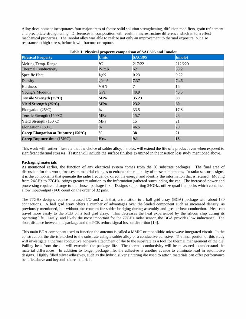
Alloy development incorporates four major areas of focus: solid solution strengthening, diffusion modifiers, grain refinement
and precipitate strengthening. Differences in composition will result in microstructure difference which in turn effect
mechanical properties. The Innolot alloy was able to realize not only an improvement to thermal exposure, but also
resistance to high stress, before it will fracture or rupture.
Table 1. Physical property comparison of SAC305 and Innolot
Physical Property Units SAC305 Innolot
Melting Temp. Range °C 217/221 212/220
Thermal Conductivity W/mK 62 55.2
Specific Heat J/gK 0.23 0.22
Density g/cm3 7.37 7.46
Hardness VHN 7 15
Young’s Modulus GPa 49.9 46.5
Tensile Strength (25°C) MPa 35.23 83
Yield Strength (25°C) MPa 23.2 60
Elongation (25°C) % 33.5 17.8
Tensile Strength (150°C) MPa 15.7 23
Yield Strength (150°C) MPa 15 21
Elongation (150°C) % 46.5 20
Creep Elongation at Rupture (150°C) % 38 21
Creep Rupture time (150°C) Hrs. 9.1 18
This work will further illustrate that the choice of solder alloy, Innolot, will extend the life of a product even when exposed to
significant thermal stresses. Testing will include the surface finishes examined in the insertion loss study mentioned above.
Packaging materials
As mentioned earlier, the function of any electrical system comes from the IC substrate packages. The final area of
discussion for this work, focuses on material changes to enhance the reliability of these components. In radar sensor designs,
it is the components that generate the radio frequency, direct the energy, and identify the information that is retuned. Moving
from 24GHz to 77GHz, brings greater resolution to the information gathered surrounding the car. The increased power and
processing require a change to the chosen package first. Designs supporting 24GHz, utilize quad flat packs which contained
a low input/output (I/O) count on the order of 32 pins.
The 77GHz designs require increased I/O and with that, a transition to a ball grid array (BGA) package with about 180
connections. A ball grid array offers a number of advantages over the leaded component such as increased density, as
previously mentioned, but without the concern for solder bridging during assembly and greater heat conduction. Heat can
travel more easily to the PCB on a ball grid array. This decreases the heat experienced by the silicon chip during its
operating life. Lastly, and likely the most important for the 77GHz radar sensor, the BGA provides low inductance. The
short distance between the package and the PCB reduce signal loss or distortion [14].
This main BGA component used to function the antenna is called a MMIC or monolithic microwave integrated circuit. In the
construction, the die is attached to the substrate using a solder alloy or a conductive adhesive. The final portion of this study
will investigate a thermal conductive adhesive attachment of die to the substrate as a tool for thermal management of the die.
Pulling heat from the die will extended the package life. The thermal conductivity will be measured to understand the
material differences. In addition to longer package life, the adhesive is another avenue to eliminate lead in automotive
designs. Highly filled silver adhesives, such as the hybrid silver sintering die used to attach materials can offer performance
benefits above and beyond solder materials.

Figure 3: Cross section of die attached by thermal conductive adhesive
One of the first areas of concern is getting a previously stored package through standard assembly processing. The defect of
concern is delamination of the epoxy mold compound with reflow exposure. During storage, packages can absorb moisture
prior to assembly. There is a risk that the heat from the reflow will volatilize the moisture, thereby putting pressure on the
epoxy and pushing that epoxy from the rest of the package, resulting in a defect known as “popcorning.”
All packages are rated on a moisture sensitivity level grading as documented by IPC J-Std 020D, a moisture sensitivity
classification for non-hermetically sealed surface mount devices [15]. End users want to ensure the components can be
stored for extended time prior to assembly and that they function reliably in their final build. Though more of a concern for
leadframe packages, attention should be paid to all larger devices especially for critical applications. This testing will ensure
that changes made for improved thermal transfer from the die, will not adversely affect overall package construction.
Table 2. IPC/JEDEC J-STD-20D MSL classification
Automotive test conditions
The automotive industry has always relied on accelerated tests such as thermal cycling in air to predict the quality of a design
and its model’s ultimate product life expectancy. Principles derived from the Coffin-Manson equation enables predictive
modeling of solder joint lifespan by accounting for the effect of plastic deformation of a material over a specified temperature
range and dwell time [12]. The resulting equation predicts that the rate of deformation of the solder joint will increase as
temperature extremes become further apart and cycle time increases. Radar designs serve a critical role in safety as the
automotive industry moves towards complete vehicle autonomy. As such, the performance requirements of the devices are
held to a higher standard. The market defined levels for high and low temperature ranges are typically based on expected
operating temperatures of the device. For example, interior systems are tested to a lower peak temperature than those for
engine control simply due to the operating environment. Safety systems such as radar start to blur the lines because they may
or may not be located in harsh areas. Also, the duration or length of the accelerated tests have been increased for safety
systems due to their critical nature.
Table 3. Thermal cycle test conditions
Test condition Duration (cycles) requirements
Powertrain Body ADAS Chassis & Safety Infotainment
Temperature
cycling
-40 / 150 °C 2000 2000 2000
-40 / 125 °C 2000 3000 3000 1000
-40 / 105 °C 1500
To simulate the environments of automotive electronics, accelerated tests are used specific to functioning electronics. They
include thermal cycling and sensitivity to moisture.
Test procedures
For this experimentation each material change was tested separately to understand its full performance improvement or lack
thereof. For a production build, it is recommended to test the parts both separately and as a full construction to understand
the improvements that can be realized for a specific application. To test the various levels of the PCBA, automotive industry
methods were used. All reflow processes were held to the IPC J-Std reflow profile which is considered a more aggressive
profile due to the long soak zone and high peak temperature. For all testing, a peak temp of 250C was used. Thermal
cycling was tested against an aggressive thermal cycling profile of -40C to 160C, with 10 min dwell, for 2000 cycles.
Surface finish effect on insertion loss
To understand insertion loss differences between surface finishes, the microstrip differential phase length method was used.
Microstrip test vehicles created from a leading PTFE substrate material specifically used for 77GHz radar designs, were
fabricated in a production environment. The strips were processed in pairs measuring 50.8 and 203.2 mm (2’ and 8”) length
each having a width of 0.75”. For ease of handling the 5-mil thick PTFE based material was adhered to an FR4 backing layer
for rigidity. The test vehicles were plated with the following production available surface finishes; high temperature organic
solderability preservative (OSP), immersion silver (Imm Ag) and immersion tin (Imm Sn). Each finish was coated to both a
thin and thick level following technical datasheet process parameters and conditions. This was chosen to illustrate any effect
of oxidation due to coating porosity for the OSP and immersion silver, or any influence of the immersion tin intermetallic
compound growth. In addition to the microstrips, specific thickness coupons were added for separate thickness
measurements based on the requirements for each surface finish. These included strip and UV absorption of the OSP, and
coulometric reduction of the tin, to determine pure tin versus intermetallic compounds which may have formed under
conditioning.
Factors
• Surface finish: organic solderability preservative, immersion silver, immersion tin
• Coating thickness:
o OSP 0.2 and 0.6 microns
o immersion silver 0.15 and 0.25 microns
o immersion tin 1.0 and 1.3 microns
• Conditioning: two reflow exposures with 250C peak temperature
Responses
• Plated thickness: ultra violet visible absorption, x-ray fluorescence and electrochemical reduction
• Growth of tin IMC – coulometric reduction analysis
• Appearance before and after conditioning – visible
• Insertion loss
After coating of the surface finishes, the thickness was determined on thickness test coupons using a UV dissolution method
for the OSP, x-ray fluorescence for the silver and coulometric reduction for tin.
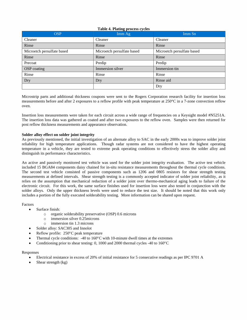
Table 4. Plating process cycles
OSP Imm Ag Imm Sn
Cleaner Cleaner Cleaner
Rinse Rinse Rinse
Microetch persulfate based Microetch persulfate based Microetch persulfate based
Rinse Rinse Rinse
Precoat Predip Predip
OSP coating Immersion silver Immersion tin
Rinse Rinse Rinse
Dry Dry Rinse aid
Dry
Microstrip parts and additional thickness coupons were sent to the Rogers Corporation research facility for insertion loss
measurements before and after 2 exposures to a reflow profile with peak temperature at 250°C in a 7-zone convection reflow
oven.
Insertion loss measurements were taken for each circuit across a wide range of frequencies on a Keysight model #N5251A.
The insertion loss data was gathered as coated and after two exposures to the reflow oven. Samples were then returned for
post reflow thickness measurements and appearance observation.
Solder alloy effect on solder joint integrity
As previously mentioned, the initial investigation of an alternate alloy to SAC in the early 2000s was to improve solder joint
reliability for high temperature applications. Though radar systems are not considered to have the highest operating
temperature in a vehicle, they are tested to extreme peak operating conditions to effectively stress the solder alloy and
distinguish its performance characteristics.
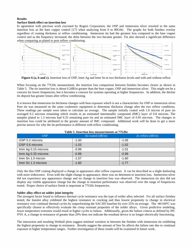
An active and passively monitored test vehicle was used for the solder joint integrity evaluation. The active test vehicle
included 15 BGA84 components daisy chained for in-situ resistance measurements throughout the thermal cycle conditions.
The second test vehicle consisted of passive components such as 1206 and 0805 resistors for shear strength testing
measurements at defined intervals. Shear strength testing is a commonly accepted indicator of solder joint reliability, as it
relies on the assumption that mechanical reduction of a solder joint over thermo-mechanical aging leads to failure of the
electronic circuit. For this work, the same surface finishes used for insertion loss were also tested in conjunction with the
solder alloys. Only the upper thickness levels were used to reduce the test size. It should be noted that this work only
includes a portion of the fully executed solderability testing. More information can be shared upon request.
Factors
• Surface finish:
o organic solderability preservative (OSP) 0.6 microns
o immersion silver 0.25microns
o immersion tin 1.3 microns
• Solder alloy: SAC305 and Innolot
• Reflow profile: 250C peak temperature
• Thermal cycle conditions: -40 to 160C with 10-minute dwell times at the extremes
• Conditioning prior to shear testing: 0, 1000 and 2000 thermal cycles -40 to 160C
Responses
• Electrical resistance in excess of 20% of initial resistance for 5 consecutive readings as per IPC 9701 A
• Shear strength (kg)
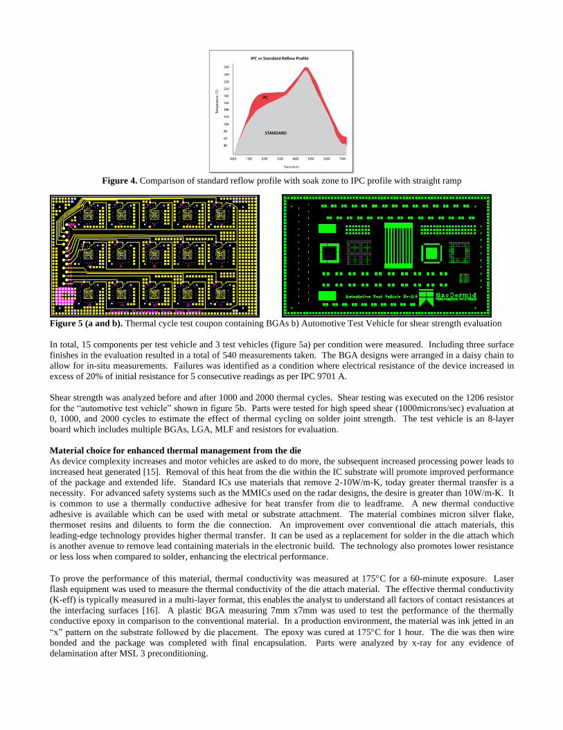
Figure 4. Comparison of standard reflow profile with soak zone to IPC profile with straight ramp
Figure 5 (a and b). Thermal cycle test coupon containing BGAs b) Automotive Test Vehicle for shear strength evaluation
In total, 15 components per test vehicle and 3 test vehicles (figure 5a) per condition were measured. Including three surface
finishes in the evaluation resulted in a total of 540 measurements taken. The BGA designs were arranged in a daisy chain to
allow for in-situ measurements. Failures was identified as a condition where electrical resistance of the device increased in
excess of 20% of initial resistance for 5 consecutive readings as per IPC 9701 A.
Shear strength was analyzed before and after 1000 and 2000 thermal cycles. Shear testing was executed on the 1206 resistor
for the “automotive test vehicle” shown in figure 5b. Parts were tested for high speed shear (1000microns/sec) evaluation at
0, 1000, and 2000 cycles to estimate the effect of thermal cycling on solder joint strength. The test vehicle is an 8-layer
board which includes multiple BGAs, LGA, MLF and resistors for evaluation.
Material choice for enhanced thermal management from the die
As device complexity increases and motor vehicles are asked to do more, the subsequent increased processing power leads to
increased heat generated [15]. Removal of this heat from the die within the IC substrate will promote improved performance
of the package and extended life. Standard ICs use materials that remove 2-10W/m-K, today greater thermal transfer is a
necessity. For advanced safety systems such as the MMICs used on the radar designs, the desire is greater than 10W/m-K. It
is common to use a thermally conductive adhesive for heat transfer from die to leadframe. A new thermal conductive
adhesive is available which can be used with metal or substrate attachment. The material combines micron silver flake,
thermoset resins and diluents to form the die connection. An improvement over conventional die attach materials, this
leading-edge technology provides higher thermal transfer. It can be used as a replacement for solder in the die attach which
is another avenue to remove lead containing materials in the electronic build. The technology also promotes lower resistance
or less loss when compared to solder, enhancing the electrical performance.
To prove the performance of this material, thermal conductivity was measured at 175C for a 60-minute exposure. Laser
flash equipment was used to measure the thermal conductivity of the die attach material. The effective thermal conductivity
(K-eff) is typically measured in a multi-layer format, this enables the analyst to understand all factors of contact resistances at
the interfacing surfaces [16]. A plastic BGA measuring 7mm x7mm was used to test the performance of the thermally
conductive epoxy in comparison to the conventional material. In a production environment, the material was ink jetted in an
“x” pattern on the substrate followed by die placement. The epoxy was cured at 175C for 1 hour. The die was then wire
bonded and the package was completed with final encapsulation. Parts were analyzed by x-ray for any evidence of
delamination after MSL 3 preconditioning.
Results
Surface finish effect on insertion loss
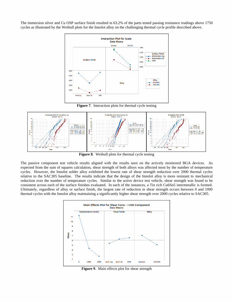
In agreement with previous work executed by Rogers Corporation, the OSP and immersion silver resulted in the same
insertion loss as the bare copper control [17] when analyzing from 0 to 80GHz. The graphs for both finishes overlay
regardless of coating thickness or reflow conditioning. Immersion tin had the greatest loss compared to the bare copper
control and as the frequency increased, the delta between the two became greater. Tin also showed a significant difference
when comparing as plated to post reflow conditioning.
Figure 6 (a, b and c). Insertion loss of OSP, Imm Ag and Imm Sn at two thickness levels and with and without reflow
When focusing on the 77GHz measurement, the insertion loss comparison between finishes becomes clearer as shown in
Table 5. The tin insertion loss is about 0.2dB/in greater than the bare copper, OSP and immersion silver. This might not be a
concern for lower frequencies, but it becomes a concern for systems operating at higher frequencies. In addition, the thicker
tin deposit has greater losses after reflow conditioning.
It is known that immersion tin thickness changes with heat exposure which is not a characteristic for OSP or immersion silver.
Pure tin was measured on the same coulmetric equipment to determine thickness change after the two reflow conditions.
Three readings per sample were taken to calculate an average. The sample initially coated with 1.0 micron of pure tin
averaged 0.2 microns remaining which results in an estimated intermetallic compound (IMC) layer of 0.8 microns. The
samples plated to 1.3 microns had 0.35 remaining pure tin and an estimated IMC layer of 0.95 microns. The changes in
insertion loss could be attributed to the greater amount of IMC compound. Additional work will be done to get a more
precise answer for why the tin performance is different with reflow conditioning.
Table 5. Insertion loss measurements at 77GHz
OSP As coated (dB/in) 2x reflow (dB/in)
OSP 0.2 microns -1.00 -1.05
OSP 0.6 microns -1.03 -1.02
Imm Ag 0.15 microns -0.99 -1.01
Imm Ag 0.33 microns -0.99 -0.99
Imm Sn 1.0 micron -1.57 -1.60
Imm Sn 1.3 microns -1.60 -1.77
Only the thin OSP coating displayed a change in appearance after reflow exposure. It can be described as a slight darkening
with more iridescence. Even with the slight change in appearance, there was no detriment to insertion loss. Immersion silver
did not experience any appearance change and no change in insertion loss was observed. The immersion tin also did not
display any visible appearance change but the change in insertion performance was observed over the range of frequencies
tested. Proper choice of surface finish is important at 77GHz frequencies.
Solder alloy effect on solder joint integrity
The strongest factor found to influence thermal cycle resistance was the type of solder alloy selected. For all surface finishes
tested, the Innolot alloy exhibited the highest resistance to cracking and thus lowest propensity to change in electrical
resistance over continual thermal cycles by outperforming the SAC305 baseline by over 25% on average. The -40/160ºC was
specifically chosen to effectively evaluate the creep resistant properties of the solder alloys. Given predictive modeling,
lower temperature extremes would result in higher cycles to failure. Additionally, given the failure criteria as defined by IPC
9701 A, a change in resistance of greater than 20% does not indicate the resultant device is no longer electrically functioning.
The interaction and resulting Weibull plots suggest minimal variation in between the finishes with immersion tin exhibiting
the highest propensity to change in resistance. Results suggest the amount of free Sn affects the failure rate due to continual
exposure to higher temperature ranges. Further investigation of these results will be examined in future work.
The immersion silver and Cu OSP surface finish resulted in 63.2% of the parts tested passing resistance readings above 1750
cycles as illustrated by the Weibull plots for the Innolot alloy on the challenging thermal cycle profile described above.
Figure 7. Interaction plots for thermal cycle testing
Figure 8. Weibull plots for thermal cycle testing
The passive component test vehicle results aligned with the results seen on the actively monitored BGA devices. As
expected from the sum of squares calculation, shear strength of both alloys was affected most by the number of temperature
cycles. However, the Innolot solder alloy exhibited the lowest rate of shear strength reduction over 2000 thermal cycles
relative to the SAC305 baseline. The results indicate that the design of the Innolot alloy is more resistant to mechanical
reduction over the number of temperature cycles. Similar to the active device test vehicle, shear strength was found to be
consistent across each of the surface finishes evaluated. In each of the instances, a Tin rich Cu6Sn5 intermetallic is formed.
Ultimately, regardless of alloy or surface finish, the largest rate of reduction in shear strength occurs between 0 and 1000
thermal cycles with the Innolot alloy maintaining a significantly higher shear strength over 2000 cycles relative to SAC305.
Figure 9. Main effects plot for shear strength
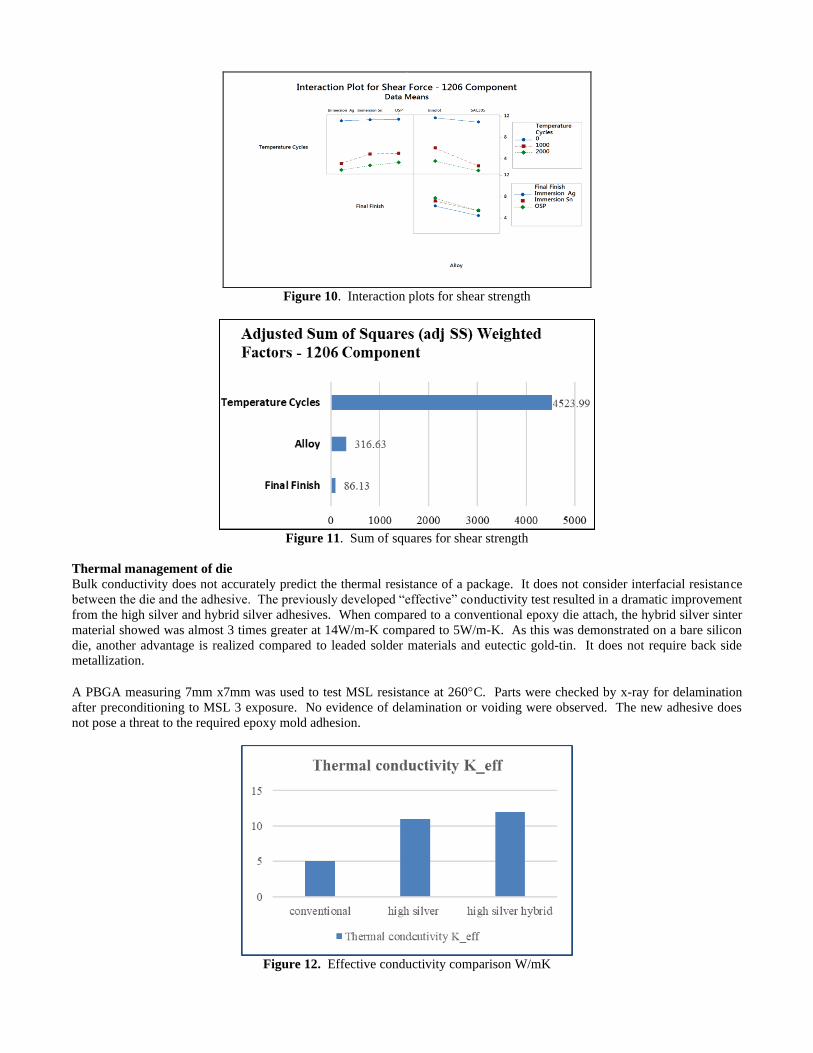
Figure 10. Interaction plots for shear strength
Figure 11. Sum of squares for shear strength
Thermal management of die
Bulk conductivity does not accurately predict the thermal resistance of a package. It does not consider interfacial resistance
between the die and the adhesive. The previously developed “effective” conductivity test resulted in a dramatic improvement
from the high silver and hybrid silver adhesives. When compared to a conventional epoxy die attach, the hybrid silver sinter
material showed was almost 3 times greater at 14W/m-K compared to 5W/m-K. As this was demonstrated on a bare silicon
die, another advantage is realized compared to leaded solder materials and eutectic gold-tin. It does not require back side
metallization.
A PBGA measuring 7mm x7mm was used to test MSL resistance at 260C. Parts were checked by x-ray for delamination
after preconditioning to MSL 3 exposure. No evidence of delamination or voiding were observed. The new adhesive does
not pose a threat to the required epoxy mold adhesion.
Figure 12. Effective conductivity comparison W/mK

Figure 13. X-ray images to determine adhesion loss
Conclusions
Significant advances are happening in the automotive space to deliver greater safety to passengers and pedestrians around the
vehicle. These enhanced safety requirements utilize specialized technologies with enhanced requirements to achieve success.
AS this research demonstrates it is imperative that the proper surface finish be chosen for high frequency applications.
Enhanced solder alloys such as Innolot are a requirement to withstand the aggressive thermal cycle conditions required for
advanced safety. Innolot in this testing shows a dramatic increase in thermal cycle resistance with superior shear strength.
Lastly, the hybrid silver sintering adhesive will also extend product life by improving the thermal transfer away from the die.
Each of these materials provides improvements over the incumbent but could realize even greater improvement when used
together in one design. It is critical to test individual material changes as well as those combined in the final design build for
a complete understanding of end use life and performance.
Acknowledgements
This work was a group effort, I’d like to extend a my appreciation to all those involved including the MacDermid Alpha
circuitry, assembly and semiconductors groups, the Rogers’ team and my marketing team for all their help.
References
[1] https://www.synopsys.com/automotive/autonomous-driving-levels.html
[2] www.pathpartnertech.com
[3] https://en.wikipedia.org/wiki/Dissipation_factor
[4] Miki,Y.; Fukunaga, T.; Yamagishi, S.; Kuwayama, I. Milimeter-Wave Automotive Antenna Using Low-Loss Fluoro-
resin Substrates. April 2019 SEI Technology Review Number 88, pp. 99-103.
[4a] http://www.ti.com/lit/wp/spry312/spry312.pdf
[5] https://www.edn.com/design/automotive/4458884/Moving-from-24-GHz-to-77-GHz-radar
[6] https://www.rogerscorp.com/documents/2122/acm/articles/Understanding-When-To-Use-FR-4-Or-High-Frequency-
Laminates.pdf
[7] Miric, A. New Developments in High-Temperature Lead-Free Solder Alloys. SMTA International Conference Orlando
Florida Oct 2010.
[8] https://www.phase-trans.msm.cam.ac.uk/2004/creep.practical.pdf
[9] Hwang, J. and Vargas, R. “Solder Joint Reliability – Can Solder Creep?”. Soldering & Surface Mount Technology, 1990
Vol. 2 No. 2, pp 38-45.
[10] Zhang, J. et al. “Correlation of aging effects on creep rate and reliability in lead free solder joints” SMTA Journal, 2012
Vol. 25 Issue 3, pp 19-28.
[11] https://www.eetimes.com/document.asp?doc_id=1149536#
[12] https://www.dfrsolutions.com/hubfs/Resources/services/Reality-of-High-Reliability-Solders.pdf
[13] Wikipedia
[14] www.ipc.org
[15] https://www.cypress.com/file/38656/download
[16] Jin, Kanagavel, and Chin. “Novel Conductive Paste Using Hybrid Silver Sintering Technology for High Reliability
Power Semiconductor Packaging.” ECTC Orlando Florida 2014.
[17] Coonrod, John. “The Impact of Final Plated Finishes on Insertion Loss for High Frequency PCBs.” SMTA
Interantional Chicago 2017.