Embed Size (px)
Citation preview

Magnetic Field Sensor Using Polymer MEMS Structures for Detection of Magnetic Fields
by
Bradley E. Oldham B.A.Sc. (Honours), Simon Fraser University, (2003)
THESIS SUBMITTED IN PARTIAL FULFILLMENT OF
THE REQUIREMENTS FOR A DEGREE OF
MASTER OF APPLIED SCIENCE
In the School of Engineering Science
Faculty of Applied Science
©Bradley E. Oldham 2011 Simon Fraser University
Fall 2011
All rights reserved. However, in accordance with the Copyright Act of Canada, this work may be reproduced, without authorization, under the conditions for "Fair Dealing."
Therefore, limited reproduction of this work for the purposes of private study, research, criticism, review and news reporting is likely to be
in accordance with the law, particularly if cited appropriately.

ii
Approval
Name: Bradley E. Oldham
Degree: Master of Applied Science
Title of Thesis Magnetic Field Sensor Using Polymer MEMS Structures for Detection of Magnetic Fields
Examining Committee:
Chair: Dr. Parvaneh Saeedi. PEng
Assistant Professor, School of Engineering Science
Dr. Andrew Rawicz, PEng Senior Supervisor Professor, School of Engineering Science
Dr. Ash M. Parameswaran, PEng Supervisor Professor, School of Engineering Science
Dr. Marinko V. Sarunic, PEng Internal Examiner Assistant Professor, School of Engineering Science
Date Defended:
November 17th, 2011

Last revision: Spring 09
Declaration of Partial Copyright Licence The author, whose copyright is declared on the title page of this work, has granted to Simon Fraser University the right to lend this thesis, project or extended essay to users of the Simon Fraser University Library, and to make partial or single copies only for such users or in response to a request from the library of any other university, or other educational institution, on its own behalf or for one of its users.
The author has further granted permission to Simon Fraser University to keep or make a digital copy for use in its circulating collection (currently available to the public at the “Institutional Repository” link of the SFU Library website <www.lib.sfu.ca> at: <http://ir.lib.sfu.ca/handle/1892/112>) and, without changing the content, to translate the thesis/project or extended essays, if technically possible, to any medium or format for the purpose of preservation of the digital work.
The author has further agreed that permission for multiple copying of this work for scholarly purposes may be granted by either the author or the Dean of Graduate Studies.
It is understood that copying or publication of this work for financial gain shall not be allowed without the author’s written permission.
Permission for public performance, or limited permission for private scholarly use, of any multimedia materials forming part of this work, may have been granted by the author. This information may be found on the separately catalogued multimedia material and in the signed Partial Copyright Licence.
While licensing SFU to permit the above uses, the author retains copyright in the thesis, project or extended essays, including the right to change the work for subsequent purposes, including editing and publishing the work in whole or in part, and licensing other parties, as the author may desire.
The original Partial Copyright Licence attesting to these terms, and signed by this author, may be found in the original bound copy of this work, retained in the Simon Fraser University Archive.
Simon Fraser University Library Burnaby, BC, Canada

iii
ABSTRACT
This thesis covers the development of a magnetic sensor for application with
brain computer interfacing for the detection of motor imagery evoked potentials. For
this application, the feasibility of a resonance magnetic cantilever based sensor is
investigated via: numerical analysis for feasibility, multilayer structure for layer
integration verification, and finally flexible magnetic material characterization for
sensing element consideration.
The flexible magnetic material that is considered in this thesis is made by the
embedding of hard rare earth magnetic (Nd2Fe14B) particles into polydimethylsiloxane
(PDMS) and provides a micro-mouldable material with hard magnetic properties. This
material provides a couple advantages for design of a small magnetic sensor as it is
scalable while being made of a rugged polymer. Additionally, this magnetic material
exhibits magnetic rheological properties when exposed to a static magnetic field. While
there is additional work needed to complete the sensor design, this thesis shows the
feasibility of this design.

iv
ACKNOWLEDGEMENTS
This thesis would not have been possible without the assistance from numerous people.
Andrew Rawicz provided the idea and provided guidance from the start to the end of
this process. Without his patience and dedication this project would have not been
possible.
Ash. Parameswaran and his team provided microfabrication expertise and access to
processes which I applied. Of particular note are See-Ho Tsang and Ajit Khosla who
personally spent numerous hours sharing process information and analysing results.
A thank-you goes to Marinko Sarunic for partaking in this process and providing
assistance. Finally, I would like to thank family and friends for seeing me through this
over the years and through the research and writing of this thesis.

v
TABLE OF CONTENTS
APPROVAL ...................................................................................................................................................... II ABSTRACT ..................................................................................................................................................... III ACKNOWLEDGEMENTS ..................................................................................................................................... IV TABLE OF CONTENTS ........................................................................................................................................ V LIST OF FIGURES ............................................................................................................................................ VII LIST OF TABLES .............................................................................................................................................. VIII
1 Introduction ....................................................................................................................................... 1 1.1 MOTIVATIONS ...................................................................................................................................... 1 1.2 THEORY ............................................................................................................................................... 3
1.2.1 Brain Computer Interface ....................................................................................................... 3 1.2.2 Magnetic Sensors .................................................................................................................... 4 1.2.3 MEMS (Micro Electrical Mechanical Systems) ........................................................................ 6 1.2.4 Resonance Sensor Design ....................................................................................................... 7
2 Finite Element Analysis of a Magnetic Resonance Sensor ................................................................... 9 2.1 RESONANCE DESIGN .............................................................................................................................. 9 2.2 FORCE ANALYSIS ................................................................................................................................. 10 2.3 FINITE ELEMENT ANALYSIS RESULTS ........................................................................................................ 11 2.4 CONCEPTS ......................................................................................................................................... 13 2.5 LESSONS LEARNED ............................................................................................................................... 14
3 Fabrication of Multilayer Polyimide Cantilevers ............................................................................... 15 3.1 ENCAPSULATED DESIGN ........................................................................................................................ 15 3.2 DEVICES FABRICATED ........................................................................................................................... 16 3.3 FABRICATION PROCESSES AND CHALLENGES ............................................................................................. 17
3.3.1 Electroplating Fe ................................................................................................................... 18 3.3.2 Unintended Insulation Layer ................................................................................................. 18
3.4 LESSONS LEARNED ............................................................................................................................... 19
4 Fabrication of MicroMolded Magnetic PDMS Cantilever .................................................................. 21 4.1 DEVICE SPECIFIC THEORY ...................................................................................................................... 21 4.2 DEVICE DESIGN ................................................................................................................................... 22 4.3 DEVICE FABRICATION PROCESSES ........................................................................................................... 22
4.3.1 Materials:.............................................................................................................................. 22 4.3.2 Process .................................................................................................................................. 23
4.4 CHARACTERIZED DEVICE ....................................................................................................................... 24
vi
5 Deflection Results of PDMS Cantilever ............................................................................................. 25 5.1 STATIC DEFLECTION OF DEVICES ............................................................................................................. 25
5.1.1 PDMS Cantilever deflection .................................................................................................. 26 5.1.2 SU-8 Cantilever deflection .................................................................................................... 27 5.1.3 Deflection Comparison .......................................................................................................... 27
5.2 DYNAMIC DEFLECTION OF PDMS CANTILEVER ......................................................................................... 28 5.2.1 Apparatus ............................................................................................................................. 28 5.2.2 Actuation Coils ...................................................................................................................... 30 5.2.3 Device Orientation ................................................................................................................ 31 5.2.4 System Response .................................................................................................................. 32
5.3 ANALYSIS AND COMPARISON OF PDMS STATIC AND DYNAMIC RESPONSE ..................................................... 34 5.4 THEORETICAL SENSITIVITY OF MAGNETIC PDMS BASED CANTILEVERS ........................................................... 35 5.5 SOURCES OF ERROR IN DETECTION OF CANTILEVER MOTION ....................................................................... 36
5.5.1 Direct Measurement ............................................................................................................. 37 5.5.2 Device Deviation ................................................................................................................... 39
6 Magnetic Rheological Characteristics of Magnetic pDMs .................................................................. 41 6.1 RHEOLOGICAL INVESTIGATION EQUIPMENT AND PROCESS ........................................................................... 41 6.2 RESULTS AND ANALYSIS OF RHEOLOGICAL CHARACTERISTICS ........................................................................ 43
7 Future Work ..................................................................................................................................... 45
8 Conclusions ...................................................................................................................................... 46
REFERENCES ................................................................................................................................................. 47 APPENDIX A: MATERIALS AND PROCESS FOR POLYIMIDE CANTILEVERS ..................................................................... 49 APPENDIX B: PDMS MICROMOLDING PROCESS .................................................................................................. 51 APPENDIX C: PDMS VS POLYIMIDE ................................................................................................................... 52

vii
LIST OF FIGURES
Figure 1: ANSYS Static Deflection ................................................................................................... 12
Figure 2: Resonance Frequency...................................................................................................... 13
Figure 3: Concept Resonance Design ............................................................................................. 14
Figure 4: Polyimide Devices, Cantilever ......................................................................................... 17
Figure 5: Contamination of Gold Contact (bottom right) ............................................................... 19
Figure 6: PDMS Devices Tested, Highlighted Device ...................................................................... 24
Figure 7: Static Deflection Measurement Setup ............................................................................ 25
Figure 8: Image of the PDMS Cantilever Deflecting While In Proximity to the Permanent Magnet ...................................................................................................... 26
Figure 9: SU-8 to PDMS Deflection Comparison ............................................................................ 27
Figure 10: Normalized Deflection and Distance ............................................................................. 28
Figure 11: Test Apparatus............................................................................................................... 29
Figure 12: Magnetic Field based on Location and Applied Voltage ............................................... 31
Figure 13: Field Measurement Locations ....................................................................................... 31
Figure 14: Parallel Field Device Orientation ................................................................................... 32
Figure 15: Orthogonal Field Device Orientation ............................................................................ 32
Figure 16: Cantilever at Resonance with Strobe ............................................................................ 33
Figure 17: Relative Field Strength vs Coil Voltage .......................................................................... 34
Figure 18: Deflection Relative to Field Strength............................................................................. 35
Figure 19: Accuracy Limits of Interferometry[22] .......................................................................... 36
Figure 20: Relative Camera Zoom vs. Distance from Magnet ........................................................ 38
Figure 21: Percent Error vs. Distance from Magnet for PDMS Cantilever ..................................... 39
Figure 22: Setup for Magnetic Rheological Investigation, Aligned Orientation ............................. 42
Figure 23: Resonant Frequency of Micro Cantilever with Permanent Magnet in Varying Proximity ......................................................................................................... 43

viii
LIST OF TABLES
Table 1: Comparison of Magnetic Sensor Technologies .................................................................. 5
Table 2: Summary of Lessons Learned from Polyimide Design Study ............................................ 20
Table 3: Materials for Micro-Moulding Process ............................................................................. 23
Table 4: Resonance Response of Cantilever ................................................................................... 33
Table 5: Computation of Rheological Variations ............................................................................ 44

1
1 INTRODUCTION
Many people with Muscular Dystrophy (MD) or other mobility impairing disorders have
the desire for self expression but are limited by their disorder to the extent that some become
trapped within their own bodies. These people still have intact nervous systems sufficient to
create evoked potentials (EP) resulting from motor imagery (MI), and these EPs can be detected
by a brain computer interface (BCI) and turned into commands. The drawback with the existing
BCI systems is that their pickup is electrically based rather than magnetic and therefore require
continual contact with the skin that can cause irritation. The scope of this thesis is to study the
feasibility and characteristics of a magnetic sensor for detection of the EPs from the brain.
Some of the challenges faced by such a system are: miniaturization through scalability,
sufficiently low enough detectability and having a high enough signal to noise ratio.
1.1 Motivations
As a hiker and cyclist I enjoy a freedom of movement and expression that we often take
for granted until it is lost or we meet someone that has been so constrained. This recognition
of my freedom came in the form of meeting someone who is experiencing the later stages of
MD while still expressing themselves as an artist and member of our community.
MD is a group of genetic diseases that acts through the mechanisms of the muscle
proteins and therefore impacts muscle development while not directly impacting the
neurological structure. This is not the only disease that can result in patients being mentally fit
while their bodies are constrained. One method to increase expression and mobility to the lives
of these people is through a direct expression from the brain via Brain Computer Interface
2
(BCI). Three major aspects of a BCI approach that must be solved are: brain signal acquisition,
intelligent signal processing, and development of training strategies for better brain control.
This thesis focuses on the first issue, the evaluation of sensor design material that can be
applied to developing head gear for signal acquisition that is non-invasive, light, and small.
The current technology for such a system is through the use of Electroencephalography
(EEG) but this technology is limited in a number of ways. First, EEG systems rely on EEG gels
that contain polyoxyethylene (20) cetyl ether [1] to hold the electrode onto the scalp, while this
compound is acceptable for short skin exposure, repeated and long exposure can cause slight
skin irritation[2]. Secondly, motion of the sensor relative to the skin can create noise, especially
if there is high impedance between the sensor and ground reference electrode (assuming a
10/20 electrode arrangement). Finally, detection with EEG is only of cortical activity near the
surface of the brain due to the cranial fluid shielding deeper signals. The limitations of time on
the skin and depth of detection need to be addressed by the sensor technology to provide
benefit for the patient and improve the signal detection options for BCI.
The key directions for this sensor (and therefore headgear) is for it to be non-invasive to
allow for long usage time, to be able to detect signals deep into the cortex, and to be employed
with minimal supporting hardware. Since magnetic signals allow for a totally non-invasive
approach to the problem of brain signal pickup, a picotesla sensitive magnetic sensor is
investigated that works at room temperature by employing micro electrical mechanical systems
(MEMS).
3
1.2 Theory
1.2.1 Brain Computer Interface
BCI is defined as any system that detects deterministic brain activity for the intent of
creating a communication pathway with an external device. Non-invasive BCI follows two main
divisions: Hemodynamic Response (blood oxygen level) and Nerve Impulse (NI) pickup[3].
Hemodynamic response related to neural activity is detected with a functional Magnetic
Response Imaging (fMRI) and can resolve a location of approximately 0.5mm. However, due to
detection being of blood oxygen levels, there is a delay of about 1 second between the brain
activity and the start of the signal with it peaking at 4 to 6 seconds after the change in blood
oxygen levels.[4]
Comparatively, Nerve Impulse (NI aka Action Potential) is a signal created by nerve
conduction and therefore is only speed limited due to Maxwell’s Equations. Pickup of these NI
signals can be either magnetic or electric and therefore there are a large number of sensors
technologies available. For cranial impulses, electroencephalography (EEG) has been the most
prevalent due to its early implementation and ease of setup. Recent work with BCI 2000 based
on the P300 surprise response (using EEG pickup) works reliably but not quickly due to the time
required to work through the random progression of options. Secondly, since detection of the
electric field is distorted due to cranial fluid and the skull, the resulting signal is dominated by
surface cranial activity and it is not possible to solve the inverse problem for buried signal
isolation. Comparatively in the magnetic domain, magneticencephalography (MEG) has been
used for detection and it is possible to solve the inverse problem for buried signals [5]. The
major drawback of current MEG systems is their reliance on semiconductor quantum

4
interference device (SQUID) sensors base on a superconducting Josephson junction that is
super-cooled and therefore large and non-portable.
1.2.2 Magnetic Sensors
For brain computer interface design using magnetic encephalography, the biology of the
cranial nerves defines the parameters for the magnetic field sensor. Cranial magnetic fields are
on the order of 10 to 100 femtoteslas with evoking potentials ranging from 10 to 10000
hertz[6]. Some of the existing and emerging technology used for detecting picotesla and
femtotesla are:
1. Squid: Sensitivity starts at 1 fT[7], but the major drawback is that they require
liquid helium cooling infrastructure and patient protections.
2. Non-linear Zeeman spectroscopy: Sensitivity on the order of 100 pT through use
of pumped Rb gas. The challenge is sweeping the narrow band of sensitivity or
tuning the device to the desired frequency [8]
3. Hall Effect Sensors: Planar Hall Effect Bridge Sensors exhibit sensitivities down to
100 pT[9]
With all of these technologies, consideration of the noise power is critical and is
summarized by Dave P Pappas in Table 1[10]:

5
Table 1: Comparison of Magnetic Sensor Technologies
Sensor B pt/√Hz @ 1 Hz Volume Power
SQUID V .01 1 cm3 Line
Proton s 1 1 cm3 battery
e- He4/CSAM/SERF s/s/v 1 / 5 / .001 mm3 – cm3 Battery-line
Fluxgate v 10 1 cm3 battery
GMI V 3000 0.01 mm3 battery
MR V 200 0.001 mm3 battery
Hybrid GMR/SC V .032 .1 cm3 battery
Hall V 30,000 0.001 mm3 battery
ME v 1000 1 mm3 0
Magneto-optic V 1 cm3 line
The challenges with the sensors in Table 1 for application with a mobile BCI system are
that either they are not sensitive enough or there is excessive infrastructure required which
causes the sensors to be non-mobile. To select a sufficient sensor a review of prior work on the
future of magnetic sensors by the material Measurement Laboratory of National Institute of
Standards and Technology [11] places the noise floor of a magnetic sensor as illustrated in
Equation 1
Equation 1: Magnetic Sensor Noise Floor
Additional to those of noise, there are physical constraints of a Brain Computer
Interface:

6
1. Distance between nerve and sensor 15mm[12], approximately twice that of the
thickness of the skull
a. Thickness of human skull = 7.1 mm[13]
2. Detection of Brain signal = 10 to 100 femto Tesla[6]
The above information leads to a number of requirements and directions:
1. Reducing the thickness of the device will bring the sensor closer to the brain and
therefore the stronger the signal
2. Reducing the number of sensor noise sources (ie electronics, amplifier, Johnson
and Shot, etc)
3. Smaller the area of the sensor the more sensors that can be placed on the brain
to improve resolution, but the smaller the area the less field will pass through
the sensor
1.2.3 MEMS (Micro Electrical Mechanical Systems)
Sensors design with MEMS allows for the combination of miniaturization of macro
structures and the close integration of detection electronics. The two construction methods
covered in this thesis are suspended structure by sacrificial layer and micro moulding.
Sacrificial layer designs have the advantage that structures are pre-mounted on the substrate
and ensure accurate alignment to secondary structures such as coils or sensor but there is a
requirement that all materials are compatible and manipulated by micro-fabrication processes
(chemical etching, React Ion Etching, deposition, etc.)[14]. Comparatively, micro-moulding of

7
structures allows for usage of non-compatible materials but requires more care in mounting
and post processing the structures to prevent damage or distortion.
The applications for MEMS using these two construction methods range from discrete
mass resonant biosensors [15] to direct moulding of dry adhesives [16]. This thesis will focus on
polymer cantilevers designed to work in a resonant state with different materials and created
using both sacrificial layer and micromolding techniques.
1.2.4 Resonance Sensor Design
Resonant sensors have been researched for applications such as biosensors where the
nature of the sensor has a mass varying relationship with the reactant. The characteristics of a
resonant design are covered in previous work at SFU[17]. The three key components of a
resonant sensor are (examples as per [17])
1. Cantilever (refer to formula’s below)
2. Resonant Actuator (piezoelectric actuator)
3. Position detector (detection of capacitance between cantilever and wafer)
The formulas that define the resonant cantilever are:
Equation 2: Resonant frequency of the cantilever
Equation 3: Quality factor, resolution of the resonant system
The frequency of a resonant cantilever should be targeted for detection of a brain waves
based on existing EEG bands ranging from 0 to 100+ Hz. The minimum frequency should be

8
based on Nyquest theorem at twice the maximum detection frequency and therefore near 500
Hz. The maximum frequency should be less then 1 part per million of the lower frequency and
therefore lower 1 Mhz. A target frequency between 2 kHz and 20 kHz allows for a band of
tolerance between the upper and lower limits while ensuring sufficient target area as to not
unduly constrict the design target.
This thesis investigates the design constraints and design approaches for a resonant
magnetic field sensor for application in brain computer interfacing. The first study focuses on
the design constraints assuming a “perfect” world detection of optical interference
measurement. While optical interference currently has not been miniaturized to the point of a
mobile application, it is theoretically possible. The second study investigates a possible
construction approach and detection method that leverages expertise and proven technologies
developed at Simon Fraser University (SFU) with Polyimide. While the polyimide design
experienced some build challenges with contamination at build yield, it did pave the way for
the designs micro-moulded in Section 4.

9
2 FINITE ELEMENT ANALYSIS OF A MAGNETIC RESONANCE SENSOR
This first study focuses on the finite element analysis of a resonance polymer cantilever
for application as a magnetic field sensor for brain wave detection. ANSYS design tool is used to
analyse an SU-8 cantilever. This analysis was presented at CMBES 2006 in Vancouver.
2.1 Resonance Design
MEMS has previously been used to for the fabrication of chemicals sensors by
measuring the change in weight of the sensing element at the end of a resonant
microcantilever [15]. The premise of this analysis is to replace this sensing element that
changes mass with a magnetic sensing element that responds to an external magnetic field.
Using the parameters for cranial magnetic fields listed in section 1.2.2 and the equations
described by Lange [18] for the resonance frequency of a monolithic microcantilever, this
equation can be solved (refer to Equation 4). For this analysis we use the mechanical
properties of SU-8 and the values listed below Equation 4 to provide a resonance frequency of
3.7 kHz.

10
( )22
2
0, 1122
υρλ
πω−
==E
Lh
f nnn
Equation 4: Resonant Frequency of Micro Cantilever
0.22 Ratio sPoisson' /1190Density Mass
02.4Modulus sYoung'm300Cantilever ofLength
m1Cantilever ofHeight 1.875 Constant n Integratio
Frequency Resonance ,
3
n
====
========
=
υρ
µµ
λω
mkgGpaE
Lh
f nn
As defined in Equation 3, the quality factor reflects the selectivity of a cantilever and for
this microcantilever system the relationship is inversely proportional to the length of the beam
and therefore is proportional to the resonance frequency. It should be noted that the target
resonance frequency of this system is low relative to the systems presented in Lange [18] and
thus will have a lower quality factor that results in reduced selectivity.
2.2 Force Analysis
Coulomb’s Law describes the attraction of two changed surfaces based on the electric
charge between them. If we treat magnetic in a similar fashion then we can describe two
magnetic surfaces being attracted to each other based on the change in magnetic charge
between them.
Using the magnetic charge model (rather than current loop) to define a permanent
magnet, one can compute the force generated by the human brain onto a small sensor placed
in close proximity [19][20] defined in Equation 5.

11
2221
4 rAMMF
π=
Equation 5: Force between Magnetic Devices
cm 1.5 Sensor toDistance m50 m50 Sensor of Area
T 12 Sensor Strenght, Field T 104 Brain Strength, Field
Sensoron acting Force14
==×====×==
=
rA
.MMF
sensor
sensor
-brain
µµ1
Using the values listed below Equation 5 the computation results in a force on the order
of 7*10-18N and thus equivalent to a 0.7ng mass attached to the end of the microcantilever
when in Earth’s gravity. Based on existing experiments with resonant microcantilevers using
MEMS technology, a weight of 0.54pg was detectable [15]; thus, the magnetic force of 7*10-18N
will be sufficient for detection using this theoretical cantilever.
2.3 Finite Element Analysis Results
Finite Element Analysis (FEA) analysis of a single cantilever was completed using ANSYS
8.1A1 to confirm the numerical calculations for static deflection and for resonance frequency.
The ANSYS Finite Element Analysis (FEA) package was chosen due to availability and use by
other MEMs researchers at SFU.
For static deflection the 2D simulation of a simple cantilever was done using the
material properties of SU-8 and placing a point force of 5x10⁻⁹N at the free end (refer to Figure
1). This analysis was done to confirm function and characteristics of the model.
1 Locate source of Magnetic field 4x10-14T and determine measured point (at skull or in head?)

12
Figure 1: ANSYS Static Deflection
Using this 2D model the resonance frequency of the cantilever was calculated using
harmonic actuation of the end load. A resonance frequency of about 3300Hz was lower than
that of the computational analysis, but some error was expected because of the simplified
formula used for numerical analysis (refer to Figure 2). Even with this deviation, the resonance
frequency is still inside the target frequency range of brain signals previously described in
section 1.2.2.

13
Figure 2: Resonance Frequency
2.4 Concepts
The above Ansys analysis lead to the design concept illustrated in Figure 3 that consists
of two symmetric resonance cantilevers; one magnetic, one non magnetic. By measuring the
difference in response between the non-magnetic and magnetic cantilevers separation of
motion noise (actuation be external vibration of the system) and the magnetic fields from the
brain can be differentiated. The method of detection of this design is via an optical detection
system, hence there are no pickup coils or other sensor integated (refer to Figure 3).

14
Figure 3: Concept Resonance Design
2.5 Lessons Learned
The sensitivity of this sensor showed promise through calculation; however, even
though this sensor design was not constructed it strongly influenced the future designs. The
next section is of a single magnetic sensor rather than the two because the pickup sensor is a
coil rather than an external optical system proposed in this design.
SU-8
Hard Magnet
Bulk Silicon

15
3 FABRICATION OF MULTILAYER POLYIMIDE CANTILEVERS
Based on the cantilever design requirements investigated in the previous study, this
fabrication process will also be investigating the ability to integrate the fabrication processes
with pickup coils. The three fabrication techniques used in this MEMS magnetic field sensor
are:
1. Encapsulated design of a gold planar coil encapsulated within polyimide
2. Iron electroplating onto gold with Polyimide mask
3. Compatibility of all layers with XeF2 isotropic etching
3.1 Encapsulated Design
For fabrication of the magnetic sensor there needed to be a way to prevent corrosion of
the magnetic element and reduce the chance for a change in mass at the end of the cantilever,
thus it was selected to encapsulate the magnetic element between two layers of structural
material. Some further modifications to the design presented in section 2.1 are presented
below.
1. Magnet creation or application at a designated location while being repeatable
and accurate. The use of electroplating was selected as it can be accurately
placed and controllable.
2. Pickup coil on the same wafer as the cantilever to ensure close tolerance during
construction. Use of gold coils was selected as the material is compatible with
the polyimide process.

16
3. System needs to be either entirely biocompatible or encased in a biocompatible
material. Since polyimide is biocompatible and the selected structural layer,
sandwiching the sensor and coils in polyimide was selected.
The encapsulation of the magnet in polyimide added the complexity of ensuring lattice
mismatch is handled and that there is sufficient material around the edges of encased layers to
ensure sealing that otherwise could result in de-lamination.
Due to lattice mismatch between magnetic metals (such as iron or nickel) and polyimide
adhesion is not possible and therefore requires an intermediary. The usage of gold as an
electroplating base for iron is known and it is possible to sputter the layer (unlike Iron).
3.2 Devices Fabricated
Devices that were studied in this design are simple cantilevers for process and
performance metrics (refer to Figure 4).
17
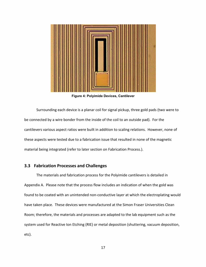
Figure 4: Polyimide Devices, Cantilever
Surrounding each device is a planar coil for signal pickup, three gold pads (two were to
be connected by a wire bonder from the inside of the coil to an outside pad). For the
cantilevers various aspect ratios were built in addition to scaling relations. However, none of
these aspects were tested due to a fabrication issue that resulted in none of the magnetic
material being integrated (refer to later section on Fabrication Process.).
3.3 Fabrication Processes and Challenges
The materials and fabrication process for the Polyimide cantilevers is detailed in
Appendix A. Please note that the process flow includes an indication of when the gold was
found to be coated with an unintended non-conductive layer at which the electroplating would
have taken place. These devices were manufactured at the Simon Fraser Universities Clean
Room; therefore, the materials and processes are adapted to the lab equipment such as the
system used for Reactive Ion Etching (RIE) or metal deposition (shuttering, vacuum deposition,
etc).

18
After completion of the process the devices are ready for testing, please note that some
of these design states are based on the processes and devices available at SFU. The following
sections review some of the process challenges that were encountered: first the electroplating
of the iron, and second the unintended non-conductive layer on the gold.
3.3.1 Electroplating Fe
The selection of iron (Fe) was due to its hard magnetic characteristics and the
application of this iron onto the wafer was through electroplating onto the gold layer below
that also acts as a coil. The challenge with the process and its application through a polyimide
mask is that the iron can work its way between the gold and polyimide and start separating the
two layers. This ingress of gold results in more gold being accessible to solution and therefore
more area is plated compared to what was desired.
3.3.2 Unintended Insulation Layer
The major reason that this study could not be fully tested was that the gold surfaces
were coated with and unintended non-conductive layer (refer to Figure 5, the gold on the
bottom of the image should be smooth). A possible reason for this layer is that the gold is
exposed to oxygen plasma and this could have modified the surface and resulted in it bonding
with the resist or other polymer in the manufacturing process.

19
Figure 5: Contamination of Gold Contact (bottom right)
3.4 Lessons Learned
The single cantilever sensors constructed with polyimide structural layers illustrated
that the design is compatible with mass production methodologies and that resolution and
alignment of the structures was successful. While the unintended insulation layer on the gold
provided a barrier to applying the magnetic material to these cantilevers, the issue is not
intrinsic to the process and could be overcome with more attention and care in contaminant
prevention. The critical component of this design is the integration of the magnetically
responsive layer (electroplated Fe) and while electroplating is an old and refined process the
application of thin film hard magnets would require some additional refinement. These
findings are summarized in Table 2.

20
Table 2: Summary of Lessons Learned from Polyimide Design Study
Challenges
Electroplating of magnets • Careful attention needed to ensure a slow and uniform plating
of Fe • Fe is not a very hard magnetic material when compared to
rare earth magnetic available today Unintended non-conductive layer
• Prevented the application of electroplating of the Fe onto the cantilevers
Orientation of magnet and field • Discovered to be the wrong orientation as per the PDMS
designs presented next
After fabrication of the last two wafers, a PDMS process with encapsulation of materials
became available at SFU. Compared to the Fe based magnet used with the polyimide
cantilevers, the PDMS allowed for integration of harder magnetic materials such as Nd2Fe14B.

21
4 FABRICATION OF MICROMOLDED MAGNETIC PDMS CANTILEVER
In the construction of the previous devices, a multi-layer process was utilized to create
the desired structure with each layer added a necessary feature. To simplify the design and
construction of the sensor, a single layer solution is used and the integration of the magnetic
properties is incorporated directly into the structural material.
4.1 Device Specific Theory
For the application of a magnetic field sensor the use of resonance phase shifting
through applied forces is a mechanism that requires the Young’s modulus of the PDMS to result
in a resonance of at least double if not higher than the frequency of the force. In the case of
the brain’s magnetic emissions, the lower Young’s modulus of PDMS is effective. Secondly, in
comparison to the Polyimide solution presented in Section 3 where the base material was
purely structural, the PDMS is mixed with Nd2Fe14B particles to provide magnetic reactance and
the device was micromoulded to provide rapid prototypes.
Static response of the device is characterized because the activation distance of the
device is an important design feature for miniaturization of a magnetic brainwave sensor due to
the fixed thickness of the human skull and tissue that separates any non-invasive sensor from
the nerves. Secondly, the resonance response of the device is characterized for consideration
of utilizing resonant phase shifting as a sensing methodology as this is sensitive to small field
changes.
22
4.2 Device Design
To keep the system simple a single microcantilever construction is constructed;
however, instead of a separate structural layer and magnetic layer this device is constructed
with a magnetic structural layer. Since the entire structure will now react to the magnetic field
the design has been modified from a uniform cantilever to a “U” cantilever so there is more
magnetic material at the end of the device and therefore will react similarly to the previous
designs with a sensing element at the end.
4.3 Device Fabrication Processes
This section describes the materials and process used in the fabrication of a micro
moulding structural magnetic micro-cantilever. The magnetic fabrication process used to
create the PDMS with imbedded particles of Nd2Fe14B. First, the materials used for the
fabrication
4.3.1 Materials:
The pairing of PDMS and Nd2Fe14B was selected due to PDMS having a low Young’s
Modulus (refer for Appendix C), Nd2Fe14B being a hard magnetic material and the allowance for
high concentrations of particles within the polymer (refer to Table 3 for supplier specifics).
The mould for this process is polycarbonate (refer to Table 3) because PDMS does not
adhere to the moulded surface, it can be etched with photo ablation by a laser and is readily
available. A CO2 laser table at SFU Surrey was used for mould creation and adjusted to about
100µm depth (exact depth depends on exposure time and material consistency with etching
done via a raster scan to reduce over etching at interfaces).

23
Table 3: Materials for Micro-Moulding Process
Component Material Comments
Base Material Sylgard 184, PDMS Manufacturer: Dow Corning
Selected due to prior experience and expertise
Magnetic Particles MQP12-5 Manufacturer: Magnequench
Developed through collaboration with SFU for material sciences
Mould Lexan Manufacturer: SABIC Innovative Plastics
PDMS does not strongly adhere to the material after curing.
4.3.2 Process
Micro Moulding was selected as the process because PDMS with imbedded Nd2Fe14B
reacts to the magnetic field and therefore does not require a supplementary material.
Additionally, micro-moulding offers the benefit of rapidly prototyping for concept verification
and small feature size. The details of the process are located in appendix B.

24
4.4 Characterized Device
Figure 6 shows a one to one cross sectional aspect ratio (0.5mm thick) serpentine PDMS
structures within a micro-mould after curing. Please note that the highlighted section in Figure
6 is the device that was placed under test for both static and dynamic response. The length of
this cantilever after securing to the stage is 10mm (overall length is about 12mm).
Figure 6: PDMS Devices Tested, Highlighted Device

25
5 DEFLECTION RESULTS OF PDMS CANTILEVER
This section looks at the static and dynamic deflection for the PDMS cantilevers. In the
case of the static deflection, the device is compared to the response of an SU-8 cantilever
manufactured with existing processes. For the dynamic response the deflection of the
cantilever at low frequency and resonance are compared to determine experimental “Q”
factor. In closing this section looks at the source of error that are present and how some of
them are mitigated during measurement.
5.1 Static Deflection of Devices
The test apparatus is kept simple and only consists of a linear stage, fixed magnetic
source (permanent magnets) and a microscope (refer to Figure 7, microscope not shown).
Figure 7: Static Deflection Measurement Setup
The distance is measured as the distance between the resting state of the cantilever and
the nearest surface of the magnets. A comparison is done to a similar SU-8 sensor as a
baseline, as SU-8 is a common MEMS polymer used in biocompatible sensors. Figure 8 shows
an example image of the cantilever taken during the test.

26
Figure 8: Image of the PDMS Cantilever Deflecting While In Proximity to the Permanent Magnet
The numbers on Figure 8 are the measurements of deflection in the image with the top
number being the ratio between the image reference frame and reality.
5.1.1 PDMS Cantilever deflection
The PDMS cantilever (as illustrated in Figure 8) is secured to a non-magnetic stage and
the deflection angle was measured for various distances. It was found that the PDMS cantilever
has an active region from 5 degrees deflection to 25 degrees that covers the region of 14 mm to
25 mm distance from the magnet (refer to Figure 9). It should be noted that when the
cantilever is in a weak magnetic field, the start of the bend is unstable and is most likely due to

27
internal material stresses and elasticity as depicted by the reduced deflection around 40mm
distance.
5.1.2 SU-8 Cantilever deflection
The same test setup was used for the SU-8 deflection as that of the PDMS deflection.
SU-8 was selected as a comparison material due to the large number of devices being created
with this material. Refer to Figure 9 for the deflection of the SU-8 cantilever.
5.1.3 Deflection Comparison
Figure 9 shows a side by side comparison of the PDMS and SU-8 deflection angles.
Figure 9: SU-8 to PDMS Deflection Comparison
When comparing the PDMS active region to that of the SU-8, for a given deflection angle
the distance the PDMS sensor is from the magnet is approximately twice that of the SU-8
sensor and thus would be sensitive to a smaller field or a source that is further away.

28
As verified in Figure 10, the cantilevers normalized responses show the same response
phenomena are at work.
Figure 10: Normalized Deflection and Distance
This normalized comparison is done to ensure that they were not responding to any
unintended artefacts.
5.2 Dynamic Deflection of PDMS Cantilever
This section covers the dynamic response of the device including at resonance.
5.2.1 Apparatus
The test apparatus consists of four major sections (as illustrated in Figure 11):
1. parallel plainer coils

29
2. adjustable coil supports
3. device stage, and
4. strobe lighting
Figure 11: Test Apparatus
The selected plainer coils are from a DVD drive since they have consistent construction
and a large open central area. These coils are mounted on two rigid plastic platforms with
liquid adhesive while great care is taken to ensure that the coils are aligned. Refer to Section
5.2.2 for the magnetic field output of the coils. The platforms have three threaded adjustments
to allow for spacing consistency; however, even though the system was designed for various
heights, central alignment of the cantilever to the middle of the upper coil provided the most
response. The platforms are set to the minimum distance that still allowed the slide to move
without rubbing on both sides (about 12 mm). For reference, the device slide is made of wood

30
to allow for easy insertion and extraction of the device while not grinding away at the
apparatus over time and being non-ferromagnetic. The strobe lighting is connected to phase
shifting circuitry to allow for visual confirmation and imaging during different angles of
operation.
5.2.2 Actuation Coils
To ensure a consistent field, four coils are placed in line with two above and two below
the device under test. The field was consistent with a maximum generated field of just under
2.0mT (refer to Figure 12 for measurements at locations shown in Figure 13). The order of
magnitude of output of the coils fields is important as the sensors are constructed in a
macroscopic fashion to minimize the need for external magnetic field shielding of the sensors
that would prevent erroneous data.

31
Figure 12: Magnetic Field based on Location and Applied Voltage
Figure 13: Field Measurement Locations
5.2.3 Device Orientation
The orientation of the device magnetization and the actuation field is critical and should
be orthogonal to ensure a torsion load is placed upon the device as this maximizes the response
and ensures the device responds in both directions. Compared to electrostatics where parallel
alignments of the fields is important (refer to Figure 14), torsion on a fixed cantilever is
maximized with an orthogonal fields (refer to Figure 15).

32
Figure 14: Parallel Field Device Orientation
Figure 15: Orthogonal Field Device Orientation
5.2.4 System Response
The dynamic response for this system is done at a low frequency and at resonance
frequency (0.188 and 21.13 Hz respectively). The low frequency is such that it is dominated by
the static deflection of the cantilever and is imaged in ambient light. By comparison, the
resonant frequency operation was imaged with the strobe lamp operational to ensure timing of
measurement. For reference, detection of resonance was done through phase change of the
cantilever when transitioning past resonance. Detection of this is aided through use of a strobe
that is actuated at the same frequency of the actuation and with a 90 degree shift in frequency.

33
At resonance the cantilever will be illuminated only on one side of rest until the actuation
frequency passes resonance at which the system (refer to images in Figure 16).
Figure 16: Cantilever at Resonance with Strobe
Finally, the both low frequency and resonance frequencies are measured at two
different voltages to ensure consistency and that the response scales with changing amplitudes.
Table 4 shows the difference in amplitude between low frequency operation and resonance.
Table 4: Resonance Response of Cantilever
Voltage Frequency Deflection Deflection /Volt
Ratio of mm/mV
% Diff
292mV 0.188 Hz 0.66 mm 0.022 mm/mV 2.78
0.11 292mV 21.13 Hz 2.27 mm 0.061 mm/mV
1000mV 0.188 Hz 1.90 mm 0.018 mm/mV 2.77
1000mV 21.16 Hz 6.36 mm 0.051 mm/mV
The impact of improved amplitude for the cantilever shows an amplitude gain of 2.78
independent of actuation voltage and with a high tolerance to error of only 0.11%. This implies
that actuation voltage can be varied for different applications to configurations while
maintaining the gain in amplitude. The difference in response between static and dynamic
response is minimal to non-existent for very slow frequencies compared to resonance (ie two

34
orders of magnitude below resonance). By comparison, resonant operation has higher
deflection and creates two benefits to improve sensitivity of a device, magnitude and
resonance phase shift. First, the increase in magnitude of resonance vs. static results in an
improved ability for detectability on the condition that the increased speed does not disrupt
detection. Secondly, there is improved sensitivity resulting from magnitude change due to
phase shift at resonant frequency described in section 1.2.4).
5.3 Analysis and Comparison of PDMS Static and Dynamic Response
Based on section “5.2.2 Actuation Coils” the field strength per volt averages 1.55 mT/V
(averaging locations C, D and E, refer to Figure 17) .
Figure 17: Relative Field Strength vs Coil Voltage
Using the coil response, a correlation between deflection and field strength can be
calculated (refer to Figure 18)

35
Coil Voltage (mV)
Deflection (mm)
Field Strength (@ 1.55mT/V)
Relative Deflection (mm
per mT)
Frequency
292mV 0.66 mm 0.453 mT 1.46 mm/mT 0.188 Hz Low
1000mV 1.90 mm 1.55 mT 1.22 mm/mT 0.188 Hz Low
292mV 2.27 mm 0.453 mT 5.01 mm/mT 21.13 Hz Resonance
1000mV 6.36 mm 1.55 mT 4.10 mm/mT 21.13 Hz Resonance
Figure 18: Deflection Relative to Field Strength
The relative field strength maps the resonance response of the cantilever of 262mV to
453µT actuation force presents a deflection of 4 to 5 mm deflection per mT. Taking into
consideration that the cantilever is 0.5mm thick this reflects a motion ratio of 8 to 10 times that
of the device thickness. Cantilever operation in a 1.55mT field shows a slightly reduced relative
deflection than the lower field strengths and this negative correlation indicates that the device
is being stressed such that a secondary effect is taking place to the point where internal
stresses or device elongation impacts the results. However, compared to if the correlation had
been the other direction this does indicate that the device can be miniaturized.
5.4 Theoretical Sensitivity of Magnetic PDMS Based Cantilevers
The sensitivity threshold of a sensor is limited in two ways: first, the detection limit of
the sensor’s response to an impulse of change; secondly, the signal to noise ratio or noise floor
of the sensor comes into effect. The detection limit is based on the resolution of the sensing
element and in the case of interferometry it is limited to between pm or nm depending on the
technology (refer to Figure 19).

36
Figure 19: Accuracy Limits of Interferometry[21]
For this example we will use the sensitivity of 4nm as the limit of the detection. Using
the 1mm/mT sensitivity listed in Figure 18 for a static response this leads to a sensitivity of 1nT
with the given geometry prior to optimization for deflection and resonance range. Given that
the resonance response of the designed sensors was only 5:1 there is room for improvement
because with an improvement to the quality factor (Q factor) a value of 10 to 100 times should
be possible through refinement. These improvements place the devices detection limit in the
neighbourhood of 10nT and therefore at the upper range of cranial magnetic signals.
5.5 Sources of Error in Detection of Cantilever Motion
Error can be broken down into two different sources: Direct Measurement and Device
Deviation. Direct Measurement reflects variance that can occur in the measurement of the
device such as through error in edge detection, image blur or focus error. Device deviation
comes from phenomena like internal device stress (temperature variance, curing stress, etc),
clustering of magnetic particles within the device or dimensional variation of the device (mould

37
or curing). Both sources of error have mitigation methods that can be applied in order to
ensure reliable results.
5.5.1 Direct Measurement
Errors from measurement resulting either from inconsistent measuring point or the
optical limitations of imaging detection methods (lens blur, and zoom variation) fundamentally
impact the reliability of choosing an accurate point of measure and accurate representation of
that point in space. One approach to reducing this error is to use parameters that scale with
zoom such as aspect ratios or angles. For this thesis, angles were used for determination of
deflection for three reasons:
1. The camera used sometimes auto-adjusted the zoom of the image slightly and
this impacts the linear measurements (PDMS data experienced a zoom change,
refer to Figure 20).

38
Figure 20: Relative Camera Zoom vs. Distance from Magnet
2. Consistent point of measure is a challenge with images due to potential
shadowing or inconsistent edge detection that resulted in a variance of value.
3. The cantilever is able to twist so the determination of the leading edge was
sometimes hard to differentiate in 2D. Figure 21 illustrates the impact of not
mitigating torsion or not averaging the leading and tailing edge (note the shift at
30mm). The values presented in Section 5.1.1 use an average of the front and
rear cantilever arms.

39
Figure 21: Percent Error vs. Distance from Magnet for PDMS Cantilever
5.5.2 Device Deviation
Device deviation comes from internal device stress (temperature variance, curing stress,
etc), clustering of magnetic particles within the device or dimensional variation of the device
(mould or curing).
Deviation either between devices or within the same device is primarily visible during
the resting state or as a non-linearity during operation of the device. If internal stresses are
present they manifest as a twisting or curling of the device while at rest and form during the
polymer’s curing phases if the curing process is not properly adhered to. A common issue is
thermal stress that occurs if the polymer is cured at too high a temperature and the
polymerization process is inconsistent throughout the device leading to one side being “tighter”
than the other (similar to how a cheesecake develops a skim during baking).

40
Compared to stresses that can permeate the entire structure of a device, clustering of
particles can create a non-linear response due to improper mixing of the particles into the
polymer or the presence of intrinsic magnetic fields within a couple particles can cause
magnetic grouping and these groups react stronger to the magnetic field compared to the rest
of the device.
Finally, dimensional deviations can occur due to incomplete mould filling or deformation
during extraction and/or handling. Predominantly, device deviation can be eliminated by
refining the device fabrication process and careful installation into whatever rig or holder the
device will finally be in. For example, placing the uncured mould into a vacuum chamber for a
couple minutes prior to curing can help remove any voids, but vibration of the device should be
minimized to prevent clustering of the particles due to the presence of standing waves that can
occur within the device.

41
6 MAGNETIC RHEOLOGICAL CHARACTERISTICS OF MAGNETIC PDMS
So far in this thesis the Young’s Modulus has been treated as a constant value, as these
fields have been dynamic and not impacted by a change in magnitude (as illustrated in Table 4).
Secondly, shielding has been used to reduce the exposure of the system to static fields. In this
section the cantilever is exposed to a static orthogonal field and illustrates the change in the
apparent Young’s Modulus, and therefore the rheological effect this field has on the material.
This section is broken down in the equipment setup, results and final analysis for
determining how the apparent Young’s Modulus is varying.
6.1 Rheological Investigation Equipment and Process
The equipment for this investigation uses the same stage, coils and cantilever as in
section 5.2.1 with the additional of an external permanent magnet. Figure 22 show the
alignment of the six pieces of equipment as numbered below:
1. permanent magnet (magnetic field aligned to the cantilever)
2. parallel plainer coils
3. adjustable coil supports
4. PDMS cantilever (standing up out of page)
5. device stage, and
6. strobe lighting (not shown)

42
Figure 22: Setup for Magnetic Rheological Investigation, Aligned Orientation
Note that the centre of the permanent magnet (item 1 of Figure 22) is aligned with the
height of the tip of the cantilever (item 4 of Figure 22). The process consists of moving the
permanent magnet progressively closer, thus increasing the static field at the cantilever. Figure
22 shows the orientation where the permanent magnet’s magnetization is aligned with that of
the cantilever; however, if this alignment is reversed the direction of change in the resonant
frequency is also reversed. The following section presents and analyses the results of this
process in both orientations.

43
6.2 Results and Analysis of Rheological Characteristics
From the process above, the change in resonance frequency of the cantilever varied
from a starting resonance of 24.1 Hz to either 21.5Hz or 26 Hz depending on the system’s
orientation (refer to Figure 23).
Figure 23: Resonant Frequency of Micro Cantilever with Permanent Magnet in Varying Proximity
Note that results for distances closer than 50mm were not possible due to mechanical
interference between the magnet and the stage.
Using the equation for resonance frequency of a cantilever (refer to Equation 4), the
relationship between resonance frequency and Young’s Modulus is:
𝜔𝑛 ∝ √𝐸 Equation 6: Natural Frequency Relation to Young's Modulus
Based on the variation in resonance frequency seen, the required variation in Young’s
Modulus is listed in Table 5.

44
Table 5: Computation of Rheological Variations
Characteristic Equation Aligned Orientation Opposing Orientation
Ratio 𝜔𝜔𝑛
21.524.1
= 0.89 26
24.1= 1.07
Young’s Modulus �𝜔𝜔𝑛�2
[0.89]2 = 0.80 [1.07]2 = 1.16
The results of up to 20% variation in Young’s Modulus (-20%/+16%) leads to two new
sensor design approaches:
1. Using an AC field for actuation and sensing a DC field through the shift of the
apparent Young’s Modulus
2. Using the change in Young’s Modulus to tune the cantilever to sense an AC field
The selection of a design approach will depend on the nature of the field being sensed,
but in the case of brain waves where the signals being sensed are so low in magnitude the
second method would be better suited.

45
7 FUTURE WORK
There are three primary directions this research can head: detection, miniaturization,
and integration. Detection of the cantilevers response to small fields and a more precise
motion detection system for the cantilever is required if the cantilever is to be integrated into
mobile systems with limited supporting structures (compared to optical detection use in this
thesis). As presented in section 5.3 the deflection of a cantilever is 8 times that of its thickness
and this provides a solid foundation to start working on miniaturization as the relative
deflection can be maintained as the device size and the field strength is reduced. Finally,
refinement of the fabrication process will allow for incorporation of other micro fabrication
processes and therefore the integration of electronic detection and actuation into the sensing
element for a more complete and unified sensor design.

46
8 CONCLUSIONS
The purpose of this thesis was to study the feasibility and characteristics of a magnetic
sensor for detection of the EPs from the brain. While this thesis did not succeed in producing a
sensor that detects magnetic fields at the level of those produced by the brain, the results from
the studies do validate the feasibility and provide strong direction for the design of such a
system. The devices fabricated from the magnetic polymer composing of Nd2Fe14B and PDMS
exhibited beneficial characteristics needed for magnetic sensor design such as scalable
resonant response and high magnetic coercivity. Such a polymer could also be integration into
a sensor design similar to those that were fabricated with the gold planar coils for actuation. A
secondary benefit of integrating this polymer into the multilayer sensor design would be to
reduce the complexity of the sensor and therefore reducing the chance of process
contamination. Finally, the resonant sensor showed very strong correlation across the field
strengths used and further reinforces the potential for design scalability.
While this study has been focused on a sensor design for a BCI other applications are
also possible such as real-time discrete magnetic spectroscopy. Other fields of application
could also exploit not only the resonant sensor design, manufacturability, low Young’s Modulus
coupled with high magnetic coercivity, but also the magnetic rheological characteristics.

47
REFERENCES
[1] D.O. Weaver. (2010, November) D.O. Weaver and Company. [Online]. http://www.doweaver.com/pdf/msds-ten20.pdf
[2] Sciencelab Inc. (2010, November) Sciencelab. [Online]. http://www.sciencelab.com/msds.php?msdsId=9927461
[3] T Berger and et al, Brain-Computer Interfaces: An International Assessment of Research and Development Trends.: Springer, 2008.
[4] (2011, August) Wikipedia, Free Encyclopedia. [Online]. http://en.wikipedia.org/wiki/Functional_magnetic_resonance_imaging
[5] Walton T. Roth, Judith M. Ford, Adolf Pfefferbaum, and Thomas R. Elbert, "Methodological Issues in Event-Related Brain Potential and Magnetic Field Studies," National Institute of Mental Health, 2000.
[6] Brian Fishbine, "Squid Magnetometry: Harnessing the Power of Tiny Magnetic Fields," Los Alamos Research Quarterly, pp. 4-11, Spring 2003.
[7] C.R. Nave. (2011, August) Hyperphysics. [Online]. http://hyperphysics.phy-astr.gsu.edu/hbase/solids/squid2.html
[8] D. Budker, W. Gawlik, and et al, "Resonant nonlinear magneto-optical effects in atoms," Review of Modern Physics, vol. 74, pp. 1153-1201, October 2002.
[9] A. Persson, R. Bejhed, K Gunnarsson, and et al., "Low-frequency picotesla field detection with planar Hall effect bridge sensors," Uppsala University, Uppsala Sweden,.
[10] Dave P Pappas. (2007, August) National Institute of Standards & Technology. [Online]. ftp://ftp.boulder.nist.gov/pub/pappas/CNRS-APS%20Sensors/CNRS7.ppt
[11] Robert Shull. (2008, October) National Institute of Standards and Technology. [Online]. http://www.nist.gov/mml/metallurgy/magnetic_materials/magnetic_sensors.cfm
[12] John P. Wikswo, John P. Barach, and John P. Freeman, "Magnetic Field of a Nerve Impulse: First Measurements," Science, vol. 208, no. 4439, pp. 53-55, 1980.
[13] Haiyan Li, Jesse Ruan, and et al., "Investigation of the critical geometric characteristics of living human skulls utilising medical image analysis techniques," vol. 2, No. 4, 2007, http://inderscience.metapress.com/index/K45772405X507K62.pdf.
[14] Dan Sameoto, K. Gupta, M. Parameswaran, and et al., "DEVELOPMENT AND APPLICATIONS OF A MULTI-USER POLYMER MEMS TECHNOLOGY," Simon Fraser University, Burnaby, PhD Thesis 2008.
[15] M. Parameswaran, A Rawicz, et al S. Prescesky, "Silicon micromachining technology for sub-nanogram discrete mass resonant biosensors," Can J. Phys, vol. 70, pp. 92-190, August 1992.
[16] C Menon D Sameoto, "Direct molding of dry adhesives with anisotropic peel strength using an offset lift-off photoresist mold ," J. Micromech. Microeng, vol. 19, no. 11, November 2009.
[17] Steven Bruce Prescesky, "Micromachined Discrete Mass Resonant Sensors," Burnaby BC,

48
1992. [18] A. Lange, O. Brand, and H. Baltes, "CMOS CANTILEVER SENSOR SYSTEMS," 2002. [19] P. Presse, "THE FORCE OF INTERACTION BETWEEN PERMANENT MAGNETS," vol. 5, no.
275-279, 1970. [20] J. Judy, "BATCH-FABRICATED FERROMAGNETIC MICROACTUATORS WITH SILICON
FLEXURES," 1996. [21] Colin E. Webb and Julian D.C. Jones, Handbook of Laser Technology and Applications:
Applications.: Taylor & Francis, 2004. [22] ALAN E. H. EMERY, MUSCULAR DYSTROPHY.: OXFORD UNIVERSITY PRESS, 2008. [23] Bradley E. Oldham and Andrew Rawicz, "NON-INVASIVE METHOD OF DETECTING ACTIVE
BRAIN SIGNALS FOR ENVIRONMENTAL CONTROL," in CMBES 29, Vancouver, 2006.

49
APPENDIX A: MATERIALS AND PROCESS FOR POLYIMIDE CANTILEVERS
Materials used: 1. Wafer selection
o 100 silicon wafer, 1mm thick or greater due to isotropic etching depth 2. Deionised water 3. RCA cleaning solution (RCA 1 is all that was performed) 4. Methanol, Acetone and other Cleanroom solutions 5. DuPont Pyralin LX PI-2610D polyimide or equivalent 6. Means of Reactive Ion Etch (RIE), 02, CF4,etc for polyimide etching 7. Adhesion promoter for selected polyimide 8. Shipley SPR2 and MF319 developer 9. Mean of creating an Oxygen plasma for activating surfaces 10. Chromium and means of sputtering 11. Gold and means of sputtering 12. Gold etchant (we used Di H2O, HNO2, HCl in a 3:1:3 ratio) 13. Chromium etchant that does not attack gold 14. Iron electroplating system 15. Aluminium and means of sputtering 16. Aluminium etchant 17. XeF2 and vacuum systems for isotropic etching of silicon
Process:
1. RCA clean wafer 2. Polyimide spin and bake
a. Cover the wafer with adhesion promoter for the polyimide, spin at 5000RPM for 30s
b. Cover with polyimide, spin starting at 500rpm, ramp up to 5000rpm over 50 s, spin 5000rpm for 70s
c. Place wafer on 80°C hot plate for 3 minutes d. Place wafer on 180°C hot plate for 3 minutes e. Ramp hot plate up to 350°C at 240°C/h f. Sustain at 350 for 30 minutes g. Let cool slowly down to room temperature (turning off hotplate and leaving until
room temperature) 3. Expose to O2 plasma (we used 50W, 0.5mtorr, sufficient flow) 4. Sputter 50nm Cr (process equipment dependent) 5. Sputter 350nm Au (process equipment dependent) 6. Spin Shipley resist 4000rpm for 30s, softbake at 100°C for 20 min 7. Expose with photolithograph (UV source dependant) 8. Develop with MF319, about 60 seconds, hardbake resist 120°C for 20 minutes 9. Gold etch (5 – 10 minutes) 10. Chromium etch (about 6 minutes)

50
11. Acetone strip resist
At this point you would normally use the process below; however, it was found on all of
our wafers there was a non-conductive coating on the gold that was not removable without
removing the chromium and gold from the wafer as well. We jumped to the final polyimide
spin and bake in step 15:
12. Repeat Shipley spin, expose and develop 13. Electroplate with Iron onto the gold openings (process dependant timing) 14. Strip resist 15. Repeat Polyimide spin and bake 16. Sputter 200nm Al 17. Repeat Shipley spin, expose and develop 18. Etch Al 19. Reactive Ion Etch (50 O2, 10 CF4, 300mtorr, 150W) for 30 minutes 20. Strip Al 21. Bake Polyimide for hardbake.
a. 80C for 3min, 150C for 3min, 450C/hr ramp to 275C for 120min b. Turn off hotplate and let cool down to room temperature
22. XeF2 etch of silicon to release structures (dependant on concentrations and vacuum levels)
23. Dice wafers as per design

51
APPENDIX B: PDMS MICROMOLDING PROCESS
The following process flow is utilized to build the PDMS cantilevers and the values in
parenthesis are suggested values:
1. Add vessel to scale
2. Add desired weight of PDMS (Sygard 184, 1.5g)
3. Add desired weight of particles in small amounts, stir continuously (MQP12-5,
3.5g, total weight is 5g)
4. Stir material until consistent
5. Place in rough vacuum for 15 to 30 minutes (removes bubbles)
6. Pour into mould and level with a straight edge
7. Place mould on hotplate to cure, (75°C for 1.5 hours, cooler and slower is better
as it reduces material stress)
8. Magnetization the devices prior to extraction (1.4 Tesla field electromagnet)

52
APPENDIX C: PDMS VS POLYIMIDE
PDMS
http://www.mit.edu/~6.777/matprops/pdms.htm
Polyimide
http://www.mit.edu/~6.777/matprops/polyimide.htm
Property Value Reference Image/URL (optional) Value Reference
Image/URL (optional)
Mass density
0.97 kg/m3 Polymer Data Handbook,
Mark J., Oxford Univ. Press, New York (1999)
1.42 g/cc
“Dupont Kapton Polyimide Film General Specifications, Bulletin GS-96-7”. http://www.dupont.com/kapton/general/H-38479-4.pdf
Young's modulus
360-870 KPa
Re-configurable Fluid Circuits by PDMS Elastomer Micromachining
http://mass.micro.uiuc.edu/ publications/papers/26.pdf
2.5 GPa
“Dupont Kapton Polyimide Film General Specifications, Bulletin GS-96-7”. http://www.dupont.com/kapton/general/H-38479-4.pdf
Poisson ratio 0.5 Polymer Data Handbook 0.34 @ 23°C
“Dupont Kapton Polyimide Film General Specifications, Bulletin GS-96-7”. http://www.dupont.com/kapton/general/H-38479-4.pdf
Tensile or fracture strength
2.24 MPa Polymer Data Handbook 231 MPa @ 23°C 139 MPa @ 200°C
“Dupont Kapton Polyimide Film General Specifications, Bulletin GS-96-7”. http://www.dupont.com/kapton/general/H-38479-4.pdf
Residual stress on silicon
35MPa @5 μm , on 8” wafer, 375°C cure
“Photodefinable HD-4000 Series Polyimide Product Bulletin.” http://www.hdmicrosystems.com
Specific heat
1.46 kJ/kg K Polymer Data Handbook 1.09 J/(g*K)
0.261 cal/(g*°C)
“Dupont Kapton Polyimide Film General Specifications, Bulletin GS-96-7”. http://www.dupont.com/kapton/general/H-38479-4.pdf
Thermal conductivity
0.15 W/m K Polymer Data Handbook 0.12 W/(mK)
2.87e-4 cal/(cm*sec*°C)
“Dupont Kapton Polyimide Film General Specifications, Bulletin GS-96-7”. http://www.dupont.com/kapton/general/H-38479-4.pdf
Dielectric constant
2.3-2.8 Polymer Data Handbook 3.4 @ 25 μm, 1kHz
“Dupont Kapton Polyimide Film General Specifications, Bulletin GS-96-7”. http://www.dupont.com/kapton/general/H-38479-4.pdf
Index of refraction
1.4 Polymer Data Handbook 1.70
“Dupont Kapton Polyimide Film General Specifications, Bulletin GS-96-7”. http://www.dupont.com/kapton/general/H-38479-4.pdf
Electrical conducti 4x10¹³ Ωm Polymer Data Handbook 1.5e17 Ωcm “Dupont Kapton Polyimide
Film General Specifications,

53
vity Bulletin GS-96-7”. http://www.dupont.com/kapton/general/H-38479-4.pdf
Magnetic permeability
0.6x106 cm3/g Polymer Data Handbook
Piezoresistivity N/A
Piezoelectricity N/A
3.8e-12c/N (in abstract) 3.8e-3c/N in table in body of paper
Tong, Yuejin, et. al. “Preparation and properties of polyimide films codoped with barium and titanium oxides.” Journal of Applied Polymer Science, v 83, n 8, 22 Feb. 2002, p 1810-16.
Wet etching method
tetrabutylammonium fluoride (C16H36FN) + n-methyl-2-pyrrolidinone (C5H9NO) 3:1
J. Garra, T. Long, J. Currie, T. Schneider, R. White, M. Paranjape, “Dry Etching of Polydimethylsiloxane for Microfluidic Systems”, Journal of
http://scitation.aip.org/journals/doc/JVTAD6-ft/vol_20/iss_3/975_1.html
TMAH developer can be used to develop exposed photoresist and etch unmasked underlying polyimide in one step.
“Product Bulletin PI-2545 Wet Etch Polyimide.” http://www.hdmicrosystems.com
Plasma etching method
CF4+O2
J. Garra, T. Long, J. Currie, T. Schneider, R. White, M. Paranjape, “Dry Etching of Polydimethylsiloxane for Microfluidic Systems”, Journal of Vacuum Science and Technology, A20, pp 975-982, 2002.
http://scitation.aip.org/journals/doc/JVTAD6-ft/vol_20/iss_3/975_1.html
Use PECVD silicon nitride mask and use O2 plasma etch, possibly with CF4
Lee, Y.K. et al. “Reactive Ion Etich of the Fluorinated Polyimide Film.” Advanced Metallization for Future ULSI. Symposium, 1996, p 455-61. Abstract.
Adhesion to silicon dioxide
Excellent Re-configurable Fluid Circuits by PDMS Elastomer Micromachining
http://mass.micro.uiuc.edu/ publications/papers/26.pdf
Varies; “A separate adhesion promoter is recommended with PI-2525, PI-2555, PI-2556 to promote adhesion to oxides and metals. PI-2575 is self priming and does not require an adhesion promoter.”
“Product Information Pyralin PI2525, PI2555, PI-2575 & PI2556.” http://www.hdmicrosystems.com
Biocompatibility
Noniritating to skin, no adverse effect on rabbits and mice, only mild inflammatory reaction when implanted
Polymer Data Handbook; Belanger MC, Marois Y. Hemocompatibility, biocompatibility, inflammatory and in vivo studies of primary reference materials low-density polyethylene and polydimethylsiloxane: a review. J Biomed Mater Res 2001;58(5):467–77.
Used in Bio-MEMS an implantable intracortical electrode array. “Polyimide also provides an ideal surface for the selective attachment of various important bioactive species onto the device in order to encourage favorable long-term reactions at the tissue-electrode interface.” “Overall polyimide is a proven biocompatible material and an excellent choice for neuroprosthetic applications.”
Rousche, P.J.; Pellinen, D.S.; Pivin, D.P., Jr.; Williams, J.C.; Vetter, R.J.; kirke, D.R.. “Flexible polyimide-based intracortical electrode arrays with bioactive capability.” Biomedical Engineering, IEEE Transactions on ,Volume: 48 , Issue: 3 , March 2001 Pages:361 - 371
Can be found using IEEE Xplore
Hydroph Highly Re-configurable Fluid http://mass.micro.uiuc.edu/ 82 degrees Ghosh, I. et al. “Surfaces

54
obicity hydrophobic, contact angle 90-120°
Circuits by PDMS Elastomer Micromachining
publications/papers/26.pdf
Properties of Chemically Modified Polyimide Films.” Journal of Adhesion Science and Technology. Vol 11. no.6. 1997. Abstract.
Melting Point -49.9–40° Knovel Critical Tables Does not melt,
Decomposes at 520°C
“Dupont Kapton Polyimide Film General Specifications, Bulletin GS-96-7”. http://www.dupont.com/kapton/general/H-38479-4.pdf