Embed Size (px)
Citation preview

Performance Motion Devices, Inc.80 Central Street
Boxborough, MA 01719
MagellanTM Motion ProcessorMC58000 Electrical Specifications
for DC Brush, Brushless DC, Microstepping, andPulse & Direction Motion Processors
Revision 2.5, April 2013

ii MC58000 Electrical Specifications
NOTICE
This document contains proprietary and confidential information of Performance Motion Devices, Inc., and is pro-tected by federal copyright law. The contents of this document may not be disclosed to third parties, translated, copied,or duplicated in any form, in whole or in part, without the express written permission of PMD.
The information contained in this document is subject to change without notice. No part of this document may bereproduced or transmitted in any form, by any means, electronic or mechanical, for any purpose, without the expresswritten permission of PMD.
Copyright 1998–2013 by Performance Motion Devices, Inc.
ATLAS, Magellan, ION, Magellan/ION, Pro-Motion, C-Motion, and VB-Motion are trademarks of PerformanceMotion Devices, Inc.

Warranty
PMD warrants performance of its products to the specifications applicable at the time of sale in accordance with PMD’s standard warranty. Testing and other quality control techniques are utilized to the extent PMD deems necessary to support this warranty. Specific testing of all parameters of each device is not necessarily performed, except those mandated by government requirements.
Performance Motion Devices, Inc. (PMD) reserves the right to make changes to its products or to discontinue any product or service without notice, and advises customers to obtain the latest version of relevant information to verify, before placing orders, that information being relied on is current and complete. All products are sold subject to the terms and conditions of sale supplied at the time of order acknowledgement, including those pertaining to warranty, patent infringement, and limitation of liability.
Safety Notice
Certain applications using semiconductor products may involve potential risks of death, personal injury, or severe property or environmental damage. Products are not designed, authorized, or warranted to be suitable for use in life support devices or systems or other critical applications. Inclusion of PMD products in such applications is understood to be fully at the customer's risk.
In order to minimize risks associated with the customer’s applications, adequate design and operating safeguards must be provided by the customer to minimize inherent procedural hazards.
Disclaimer
PMD assumes no liability for applications assistance or customer product design. PMD does not warrant or represent that any license, either express or implied, is granted under any patent right, copyright, mask work right, or other intellectual property right of PMD covering or relating to any combination, machine, or process in which such products or services might be or are used. PMD’s publication of information regarding any third party’s products or services does not constitute PMD’s approval, warranty or endorsement thereof.
MC58000 Electrical Specifications iii

Related Documents
Magellan Motion Processor User’s Guide
Complete description of the Magellan Motion Processor features and functions with detailed theory of itsoperation.
Magellan Motion Processor Programmer’s Command Reference
Descriptions of all Magellan Motion Processor commands, with coding syntax and examples, listed alphabetically for quick reference.
Pro-Motion User’s Guide
User’s guide to Pro-Motion, the easy-to-use motion system development tool and performance optimizer.Pro-Motion is a sophisticated, easy-to-use program which allows all motion parameters to be set and/orviewed, and allows all features to be exercised.
Magellan Motion Processor Developer’s Kit Manual
How to install and configure the DK58000 series and DK55000 series developer’s kit PC board.
Atlas Digital Amplifier User’s Manual
Description of the Atlas Digital Amplifier electrical and mechanical specifications along with a summary ofits operational features.
Atlas Digital Amplifier Complete Technical Reference
Complete electrical and mechanical description of the Atlas Digital Amplifier with detailed theory ofoperations.
Other Documents
Magellan Motion Processor Electrical Specifications
Contains physical and electrical characteristics, timing diagrams, pinouts, and pin descriptions for MC55000 Series, for Pulse & Direction motion processors.
ION Digital Drive User’s Manual
How to install and configure ION Digital Drives.
Prodigy-PC/104 Motion Card User’s Guide
How to install and configure the Prodigy-PC/104 motion board.
Prodigy-PCI Motion Card User’s Guide
How to install and configure the Prodigy-PCI motion board.
iv MC58000 Electrical Specifications
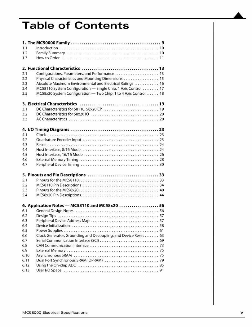
Table of Contents1. The MC50000 Family . . . . . . . . . . . . . . . . . . . . . . . . . . . . . . . . . . . . . . . . . . . 91.1 Introduction . . . . . . . . . . . . . . . . . . . . . . . . . . . . . . . . . . . . . . . . . . . . . . . . . . . . . . . . . 101.2 Family Summary . . . . . . . . . . . . . . . . . . . . . . . . . . . . . . . . . . . . . . . . . . . . . . . . . . . . . 101.3 How to Order . . . . . . . . . . . . . . . . . . . . . . . . . . . . . . . . . . . . . . . . . . . . . . . . . . . . . . . . 11
2. Functional Characteristics . . . . . . . . . . . . . . . . . . . . . . . . . . . . . . . . . . . . . 132.1 Configurations, Parameters, and Performance . . . . . . . . . . . . . . . . . . . . . . . . . 132.2 Physical Characteristics and Mounting Dimensions . . . . . . . . . . . . . . . . . . . . 152.3 Absolute Maximum Environmental and Electrical Ratings . . . . . . . . . . . . . . 162.4 MC58110 System Configuration — Single Chip, 1 Axis Control . . . . . . . . . 172.5 MC58x20 System Configuration — Two Chip, 1 to 4 Axis Control . . . . . . . 18
3. Electrical Characteristics . . . . . . . . . . . . . . . . . . . . . . . . . . . . . . . . . . . . . . 193.1 DC Characteristics for 58110, 58x20 CP . . . . . . . . . . . . . . . . . . . . . . . . . . . . . . . . 193.2 DC Characteristics for 58x20 IO . . . . . . . . . . . . . . . . . . . . . . . . . . . . . . . . . . . . . . . 203.3 AC Characteristics . . . . . . . . . . . . . . . . . . . . . . . . . . . . . . . . . . . . . . . . . . . . . . . . . . . . 20
4. I/O Timing Diagrams . . . . . . . . . . . . . . . . . . . . . . . . . . . . . . . . . . . . . . . . . . 234.1 Clock . . . . . . . . . . . . . . . . . . . . . . . . . . . . . . . . . . . . . . . . . . . . . . . . . . . . . . . . . . . . . . . . . 234.2 Quadrature Encoder Input . . . . . . . . . . . . . . . . . . . . . . . . . . . . . . . . . . . . . . . . . . . . 234.3 Reset . . . . . . . . . . . . . . . . . . . . . . . . . . . . . . . . . . . . . . . . . . . . . . . . . . . . . . . . . . . . . . . . . 244.4 Host Interface, 8/16 Mode . . . . . . . . . . . . . . . . . . . . . . . . . . . . . . . . . . . . . . . . . . . . 244.5 Host Interface, 16/16 Mode . . . . . . . . . . . . . . . . . . . . . . . . . . . . . . . . . . . . . . . . . . . 264.6 External Memory Timing . . . . . . . . . . . . . . . . . . . . . . . . . . . . . . . . . . . . . . . . . . . . . . 284.7 Peripheral Device Timing . . . . . . . . . . . . . . . . . . . . . . . . . . . . . . . . . . . . . . . . . . . . . 30
5. Pinouts and Pin Descriptions . . . . . . . . . . . . . . . . . . . . . . . . . . . . . . . . . . 335.1 Pinouts for the MC58110 . . . . . . . . . . . . . . . . . . . . . . . . . . . . . . . . . . . . . . . . . . . . . . 335.2 MC58110 Pin Descriptions . . . . . . . . . . . . . . . . . . . . . . . . . . . . . . . . . . . . . . . . . . . . 345.3 Pinouts for the MC58x20 . . . . . . . . . . . . . . . . . . . . . . . . . . . . . . . . . . . . . . . . . . . . . . 405.4 MC58x20 Pin Descriptions. . . . . . . . . . . . . . . . . . . . . . . . . . . . . . . . . . . . . . . . . . . . . 44
6. Application Notes — MC58110 and MC58x20 . . . . . . . . . . . . . . . . . . . 566.1 General Design Notes . . . . . . . . . . . . . . . . . . . . . . . . . . . . . . . . . . . . . . . . . . . . . . . . 566.2 Design Tips . . . . . . . . . . . . . . . . . . . . . . . . . . . . . . . . . . . . . . . . . . . . . . . . . . . . . . . . . . 576.3 Peripheral Device Address Map . . . . . . . . . . . . . . . . . . . . . . . . . . . . . . . . . . . . . . . 576.4 Device Initialization . . . . . . . . . . . . . . . . . . . . . . . . . . . . . . . . . . . . . . . . . . . . . . . . . . 586.5 Power Supplies . . . . . . . . . . . . . . . . . . . . . . . . . . . . . . . . . . . . . . . . . . . . . . . . . . . . . . . 616.6 Clock Generator, Grounding and Decoupling, and Device Reset . . . . . . . . 636.7 Serial Communication Interface (SCI) . . . . . . . . . . . . . . . . . . . . . . . . . . . . . . . . . . 696.8 CAN Communication Interface . . . . . . . . . . . . . . . . . . . . . . . . . . . . . . . . . . . . . . . . 736.9 External Memory . . . . . . . . . . . . . . . . . . . . . . . . . . . . . . . . . . . . . . . . . . . . . . . . . . . . . 756.10 Asynchronous SRAM . . . . . . . . . . . . . . . . . . . . . . . . . . . . . . . . . . . . . . . . . . . . . . . . . 756.11 Dual Port Synchronous SRAM (DPRAM) . . . . . . . . . . . . . . . . . . . . . . . . . . . . . . . 796.12 Using the On-chip ADC . . . . . . . . . . . . . . . . . . . . . . . . . . . . . . . . . . . . . . . . . . . . . . . 856.13 User I/O Space . . . . . . . . . . . . . . . . . . . . . . . . . . . . . . . . . . . . . . . . . . . . . . . . . . . . . . . 91
MC58000 Electrical Specifications v

Table of Contents
6.14 Parallel Word Position Input . . . . . . . . . . . . . . . . . . . . . . . . . . . . . . . . . . . . . . . . . . 936.15 Parallel Communication Interface . . . . . . . . . . . . . . . . . . . . . . . . . . . . . . . . . . . . . 956.16 Overcurrent and Emergency Braking Circuits for Motor Drivers . . . . . . . . . 996.17 DC Brush Motor Control Using SPI Interfaced DACs . . . . . . . . . . . . . . . . . . . 1016.18 Brushless DC Motor Control Using High-Precision Parallel DACs . . . . . . . 1046.19 Single-Axis Magellan with Brushless DC Atlas . . . . . . . . . . . . . . . . . . . . . . . . . 1076.20 Multi-Axis Magellan with DC Brush & Step Motor Atlas . . . . . . . . . . . . . . . . 1106.21 Pulse & Direction Mode Output Connected to Atlas . . . . . . . . . . . . . . . . . . . 1126.22 Using PWM for DC Brush, Brushless DC and Microstepping Motors. . . . . 1146.23 Using the Allegro A3977 to Drive Microstepping Motors . . . . . . . . . . . . . . 116
vi MC58000 Electrical Specifications

List of Figures
2-1 CP chip (all dimensions in millimeters) . . . . . . . . . . . . . . . . . . . . . . . . . . . . . . . . . . . . . . . .152-2 IO Chip (all dimensions in millimeters) . . . . . . . . . . . . . . . . . . . . . . . . . . . . . . . . . . . . . . .162-3 MC58110 control and data paths . . . . . . . . . . . . . . . . . . . . . . . . . . . . . . . . . . . . . . . . . . . .172-4 MC58x20 control and data paths . . . . . . . . . . . . . . . . . . . . . . . . . . . . . . . . . . . . . . . . . . . .184-1 Clock timing . . . . . . . . . . . . . . . . . . . . . . . . . . . . . . . . . . . . . . . . . . . . . . . . . . . . . . . . . . . . .234-2 Quad encoder timing . . . . . . . . . . . . . . . . . . . . . . . . . . . . . . . . . . . . . . . . . . . . . . . . . . . . .234-3 Reset timing . . . . . . . . . . . . . . . . . . . . . . . . . . . . . . . . . . . . . . . . . . . . . . . . . . . . . . . . . . . . .244-4 Instruction write, 8/16 mode . . . . . . . . . . . . . . . . . . . . . . . . . . . . . . . . . . . . . . . . . . . . . . .244-5 Data write, 8/16 mode . . . . . . . . . . . . . . . . . . . . . . . . . . . . . . . . . . . . . . . . . . . . . . . . . . . .254-6 Data read, 8/16 mode . . . . . . . . . . . . . . . . . . . . . . . . . . . . . . . . . . . . . . . . . . . . . . . . . . . . .254-7 Status read, 8/16 mode . . . . . . . . . . . . . . . . . . . . . . . . . . . . . . . . . . . . . . . . . . . . . . . . . . . .264-8 Instruction write, 16/16 mode . . . . . . . . . . . . . . . . . . . . . . . . . . . . . . . . . . . . . . . . . . . . . .264-9 Data write, 16/16 mode . . . . . . . . . . . . . . . . . . . . . . . . . . . . . . . . . . . . . . . . . . . . . . . . . . .274-10 Data read, 16/16 mode . . . . . . . . . . . . . . . . . . . . . . . . . . . . . . . . . . . . . . . . . . . . . . . . . . . .274-11 Status read, 16/16 mode . . . . . . . . . . . . . . . . . . . . . . . . . . . . . . . . . . . . . . . . . . . . . . . . . . .284-12 External memory read . . . . . . . . . . . . . . . . . . . . . . . . . . . . . . . . . . . . . . . . . . . . . . . . . . . .284-13 External memory write . . . . . . . . . . . . . . . . . . . . . . . . . . . . . . . . . . . . . . . . . . . . . . . . . . . .294-14 Peripheral device read . . . . . . . . . . . . . . . . . . . . . . . . . . . . . . . . . . . . . . . . . . . . . . . . . . . . .304-15 Peripheral device write . . . . . . . . . . . . . . . . . . . . . . . . . . . . . . . . . . . . . . . . . . . . . . . . . . . .315-1 MC58110 pinouts . . . . . . . . . . . . . . . . . . . . . . . . . . . . . . . . . . . . . . . . . . . . . . . . . . . . . . . .335-2 MC58420 pinouts . . . . . . . . . . . . . . . . . . . . . . . . . . . . . . . . . . . . . . . . . . . . . . . . . . . . . . . .405-3 MC58320 pinouts . . . . . . . . . . . . . . . . . . . . . . . . . . . . . . . . . . . . . . . . . . . . . . . . . . . . . . . .415-4 MC58220 pinouts . . . . . . . . . . . . . . . . . . . . . . . . . . . . . . . . . . . . . . . . . . . . . . . . . . . . . . . .425-5 MC58120 pinouts . . . . . . . . . . . . . . . . . . . . . . . . . . . . . . . . . . . . . . . . . . . . . . . . . . . . . . . .436-1 Basics, power supplies, 58000 . . . . . . . . . . . . . . . . . . . . . . . . . . . . . . . . . . . . . . . . . . . . . . .626-2 Basics, clock and bypass caps, 58110 . . . . . . . . . . . . . . . . . . . . . . . . . . . . . . . . . . . . . . . . .656-3 Basics, clock and bypass caps, 58420 . . . . . . . . . . . . . . . . . . . . . . . . . . . . . . . . . . . . . . . . .666-4 Oscillator filter circuit . . . . . . . . . . . . . . . . . . . . . . . . . . . . . . . . . . . . . . . . . . . . . . . . . . . . .676-5 Basics, reset . . . . . . . . . . . . . . . . . . . . . . . . . . . . . . . . . . . . . . . . . . . . . . . . . . . . . . . . . . . . .686-6 Host communication, SCI . . . . . . . . . . . . . . . . . . . . . . . . . . . . . . . . . . . . . . . . . . . . . . . . . .706-7 Host communication, RS232 and RS485/422 . . . . . . . . . . . . . . . . . . . . . . . . . . . . . . . . . . .726-8 Host communication, CANbus . . . . . . . . . . . . . . . . . . . . . . . . . . . . . . . . . . . . . . . . . . . . . .746-9 External memory, SRAM 512Kx16 . . . . . . . . . . . . . . . . . . . . . . . . . . . . . . . . . . . . . . . . . . .766-10 External memory, Ready signal generator . . . . . . . . . . . . . . . . . . . . . . . . . . . . . . . . . . . . .786-11 External memory, DPRAM, fast flow-through . . . . . . . . . . . . . . . . . . . . . . . . . . . . . . . . . .806-12 External memory, DPRAM, flow-through with clock signal control . . . . . . . . . . . . . . . . .836-13 External memory, DPRAM, RCLK timing . . . . . . . . . . . . . . . . . . . . . . . . . . . . . . . . . . . . . .846-14 External memory, DPRAM, host management . . . . . . . . . . . . . . . . . . . . . . . . . . . . . . . . . .866-15 ADC, single-ended temperature sensor . . . . . . . . . . . . . . . . . . . . . . . . . . . . . . . . . . . . . . .886-16 ADC, differential interface . . . . . . . . . . . . . . . . . . . . . . . . . . . . . . . . . . . . . . . . . . . . . . . . .906-17 User I/O space, red LED . . . . . . . . . . . . . . . . . . . . . . . . . . . . . . . . . . . . . . . . . . . . . . . . . . .926-18 Parallel word feedback, AD2S1200, 4 axes . . . . . . . . . . . . . . . . . . . . . . . . . . . . . . . . . . . .946-19 Host communication, parallel interface, 16/16 mode . . . . . . . . . . . . . . . . . . . . . . . . . . . .966-20 Host communication, parallel interface, 8/16 mode . . . . . . . . . . . . . . . . . . . . . . . . . . . . .986-21 Motor driver protection circuitry . . . . . . . . . . . . . . . . . . . . . . . . . . . . . . . . . . . . . . . . . . .1006-22 SPI DAC, DC brush, single axis . . . . . . . . . . . . . . . . . . . . . . . . . . . . . . . . . . . . . . . . . . . .1026-23 Parallel DAC, brushless DC, sheet 1 of 2 . . . . . . . . . . . . . . . . . . . . . . . . . . . . . . . . . . . .105
MC58000 Electrical Specifications vii
List of Figures
6-24 Parallel DAC, brushless DC, sheet 2 of 2 . . . . . . . . . . . . . . . . . . . . . . . . . . . . . . . . . . . . .1066-25 Brushless DC Atlas With Single-Axis Magellan . . . . . . . . . . . . . . . . . . . . . . . . . . . . . . . . .1096-26 DC Brush & Step Motor Atlas With Multi-Axis Magellan. . . . . . . . . . . . . . . . . . . . . . . . .1116-27 Step Motor Atlas Operating In Pulse & Direction Mode . . . . . . . . . . . . . . . . . . . . . . . . .1136-28 PWM, brushless DC, L6234 . . . . . . . . . . . . . . . . . . . . . . . . . . . . . . . . . . . . . . . . . . . . . . . .1156-29 PWM, DC brush, LMD18200. . . . . . . . . . . . . . . . . . . . . . . . . . . . . . . . . . . . . . . . . . . . . . .1176-30 PWM, uStep, L6202, fast decay . . . . . . . . . . . . . . . . . . . . . . . . . . . . . . . . . . . . . . . . . . . . .1196-31 PWM, uStep, L6202, mixed decay . . . . . . . . . . . . . . . . . . . . . . . . . . . . . . . . . . . . . . . . . . .1206-32 Signal state during each phase of motor output waveform. . . . . . . . . . . . . . . . . . . . . . . .1216-33 PWM, uStep, A3953S, fast decay . . . . . . . . . . . . . . . . . . . . . . . . . . . . . . . . . . . . . . . . . . . .1226-34 Encoded PWM signal spectra . . . . . . . . . . . . . . . . . . . . . . . . . . . . . . . . . . . . . . . . . . . . . . .1236-35 Filter frequency response . . . . . . . . . . . . . . . . . . . . . . . . . . . . . . . . . . . . . . . . . . . . . . . . . .1236-36 Filter output to 150 Hz electrical cycle . . . . . . . . . . . . . . . . . . . . . . . . . . . . . . . . . . . . . . .1246-37 Pulse and directon, A3977 . . . . . . . . . . . . . . . . . . . . . . . . . . . . . . . . . . . . . . . . . . . . . . . . .126
viii MC58000 Electrical Specifications
1
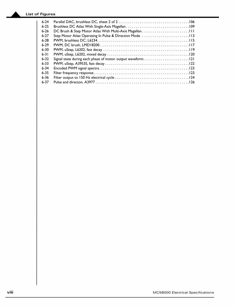
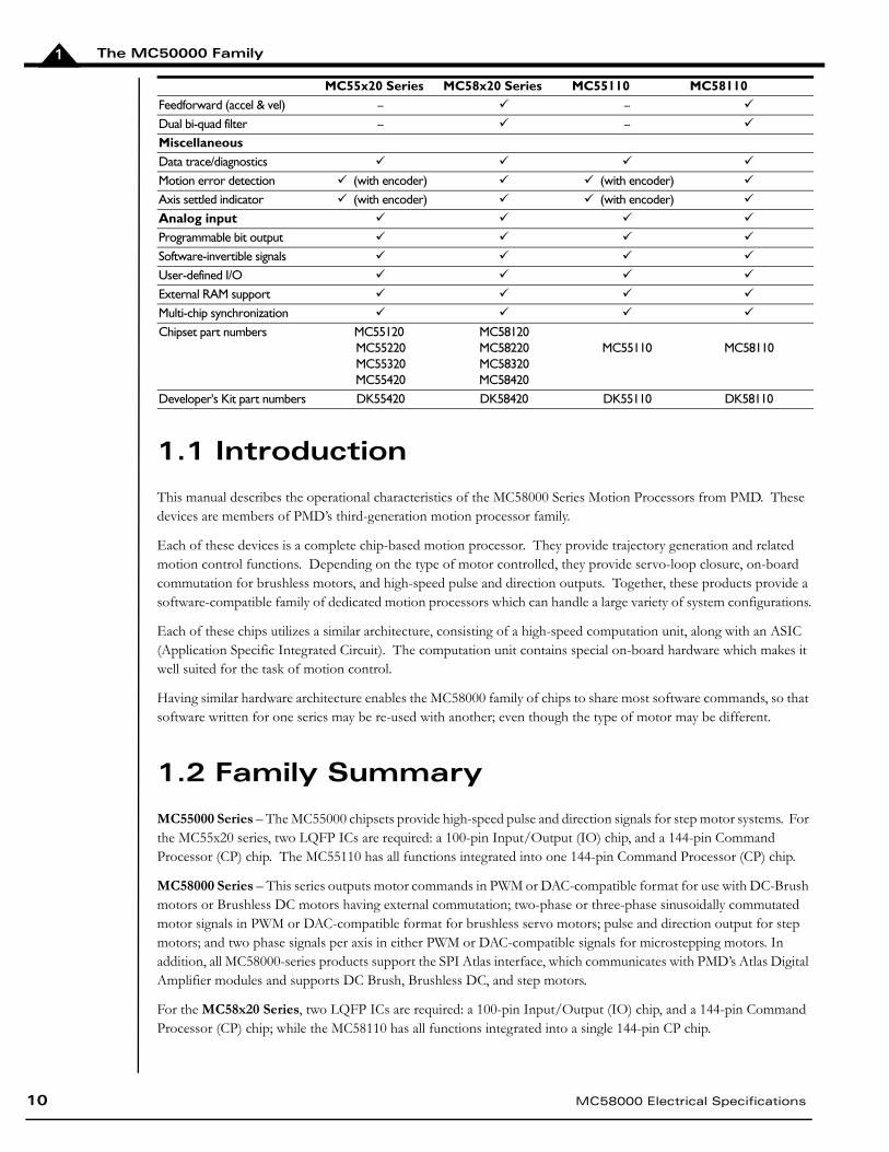
1. The MC50000 Family In This ChapterIntroductionFamily SummaryHow to OrderMC55x20 Series MC58x20 Series MC55110 MC58110Number of axes 4,3,2 or 1 4,3,2 or 1 1 1Number of chips 2 (CP and IO) 2 (CP and IO) 1 (CP) 1 (CP)Motor type Stepping DC Brush servo
Brushless DC servoStepping
Stepping DC Brush servoBrushless DC servoStepping
Output format Pulse and Direction Brushed single phaseSinusoidal commutationMicrosteppingPulse and direction SPI Atlas
Pulse and Direction Brushed single phaseSinusoidal commutationMicrosteppingPulse and direction SPI Atlas
Communication interfaceParallel
Asynchronous serial
CAN 2.0B
Position inputIncremental encoder input
Parallel word device input
Index & Home signals
Position capture
Directional limit switches
Motor command outputPWM output – –
Parallel DAC output – –
SPI DAC output – –
Pulse & Direction output
SPI Atlas – –
Trajectory generationTrapezoidal profiling
S-curve profiling
Velocity profiling
Electronic gearing
On-the-fly changes
Servo filterPID position loop – –
Dual encoder loop – – –Derivative sampling time – –
MC58000 Electrical Specifications 9
The MC50000 Family1
1.1 Introduction
This manual describes the operational characteristics of the MC58000 Series Motion Processors from PMD. These devices are members of PMD’s third-generation motion processor family.
Each of these devices is a complete chip-based motion processor. They provide trajectory generation and related motion control functions. Depending on the type of motor controlled, they provide servo-loop closure, on-board commutation for brushless motors, and high-speed pulse and direction outputs. Together, these products provide a software-compatible family of dedicated motion processors which can handle a large variety of system configurations.
Each of these chips utilizes a similar architecture, consisting of a high-speed computation unit, along with an ASIC (Application Specific Integrated Circuit). The computation unit contains special on-board hardware which makes it well suited for the task of motion control.
Having similar hardware architecture enables the MC58000 family of chips to share most software commands, so that software written for one series may be re-used with another; even though the type of motor may be different.
1.2 Family Summary
MC55000 Series – The MC55000 chipsets provide high-speed pulse and direction signals for step motor systems. For the MC55x20 series, two LQFP ICs are required: a 100-pin Input/Output (IO) chip, and a 144-pin Command Processor (CP) chip. The MC55110 has all functions integrated into one 144-pin Command Processor (CP) chip.
MC58000 Series – This series outputs motor commands in PWM or DAC-compatible format for use with DC-Brush motors or Brushless DC motors having external commutation; two-phase or three-phase sinusoidally commutated motor signals in PWM or DAC-compatible format for brushless servo motors; pulse and direction output for step motors; and two phase signals per axis in either PWM or DAC-compatible signals for microstepping motors. In addition, all MC58000-series products support the SPI Atlas interface, which communicates with PMD’s Atlas Digital Amplifier modules and supports DC Brush, Brushless DC, and step motors.
For the MC58x20 Series, two LQFP ICs are required: a 100-pin Input/Output (IO) chip, and a 144-pin Command Processor (CP) chip; while the MC58110 has all functions integrated into a single 144-pin CP chip.
Feedforward (accel & vel) – –
Dual bi-quad filter – –
MiscellaneousData trace/diagnostics
Motion error detection (with encoder) (with encoder)
Axis settled indicator (with encoder) (with encoder)
Analog input
Programmable bit output
Software-invertible signals
User-defined I/O
External RAM support
Multi-chip synchronization
Chipset part numbers MC55120 MC55220MC55320MC55420
MC58120MC58220MC58320MC58420
MC55110 MC58110
Developer's Kit part numbers DK55420 DK58420 DK55110 DK58110
MC55x20 Series MC58x20 Series MC55110 MC58110
10 MC58000 Electrical Specifications

The MC50000 Family 1
1.3 How to Order
When ordering a single-chip configuration, only the CP part number is necessary. For two-IC and multi-axis configurations, both the CP and the IO part numbers are required.
MC5 0CP . CP (1 or 2 chip configurations)
Motor Type8 = Multi Motor5 = Pulse & Direction
# Axes1,2,3,4
# Chips1 (CP only)2 (CP & IO)
CP Version(Call PMD)
MC50000IOAD8.GIO (2 chip configurations only)
DK5 0CP . IOAD8.RDeveloper’s Kit
Motor Type8 = Multi Motor5 = Pulse & Direction
# Axes1,2,3,4
# Chips1 (CP only)2 (CP & IO)
CP Version(Call PMD)
.G
MC58000 Electrical Specifications 11

The MC50000 Family1
This page intentionally left blank.
12 MC58000 Electrical Specifications
2
2. Functional Characteristics In This ChapterConfigurations, Parameters, and PerformancePhysical Characteristics and Mounting DimensionsAbsolute Maximum Environmental and Electrical Ratings — CP 58110, 58x20Absolute Maximum Environmental and Electrical Ratings — IO 58x20System Configuration — Single Chip, 1 Axis ControlMC58x20 System Configuration — Two Chip, 1 To 4 Axis Control2.1 Configurations, Parameters, and Performance
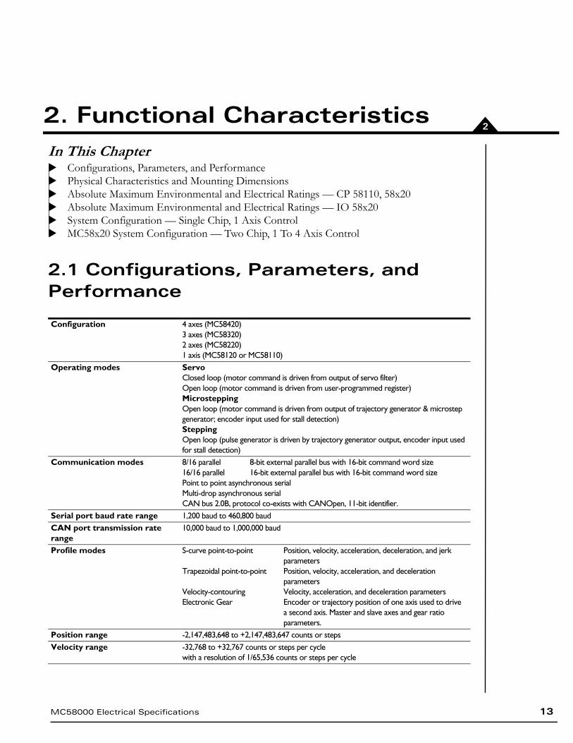
Configuration 4 axes (MC58420)3 axes (MC58320) 2 axes (MC58220) 1 axis (MC58120 or MC58110)
Operating modes ServoClosed loop (motor command is driven from output of servo filter)Open loop (motor command is driven from user-programmed register)MicrosteppingOpen loop (motor command is driven from output of trajectory generator & microstep generator; encoder input used for stall detection)SteppingOpen loop (pulse generator is driven by trajectory generator output, encoder input used for stall detection)
Communication modes 8/16 parallel 8-bit external parallel bus with 16-bit command word size16/16 parallel 16-bit external parallel bus with 16-bit command word sizePoint to point asynchronous serialMulti-drop asynchronous serialCAN bus 2.0B, protocol co-exists with CANOpen, 11-bit identifier.
Serial port baud rate range 1,200 baud to 460,800 baudCAN port transmission rate range
10,000 baud to 1,000,000 baud
Profile modes S-curve point-to-point Position, velocity, acceleration, deceleration, and jerkparameters
Trapezoidal point-to-point Position, velocity, acceleration, and decelerationparameters
Velocity-contouring Velocity, acceleration, and deceleration parametersElectronic Gear Encoder or trajectory position of one axis used to drive
a second axis. Master and slave axes and gear ratioparameters.
Position range -2,147,483,648 to +2,147,483,647 counts or stepsVelocity range -32,768 to +32,767 counts or steps per cycle
with a resolution of 1/65,536 counts or steps per cycle
MC58000 Electrical Specifications 13
Functional Characteristics2
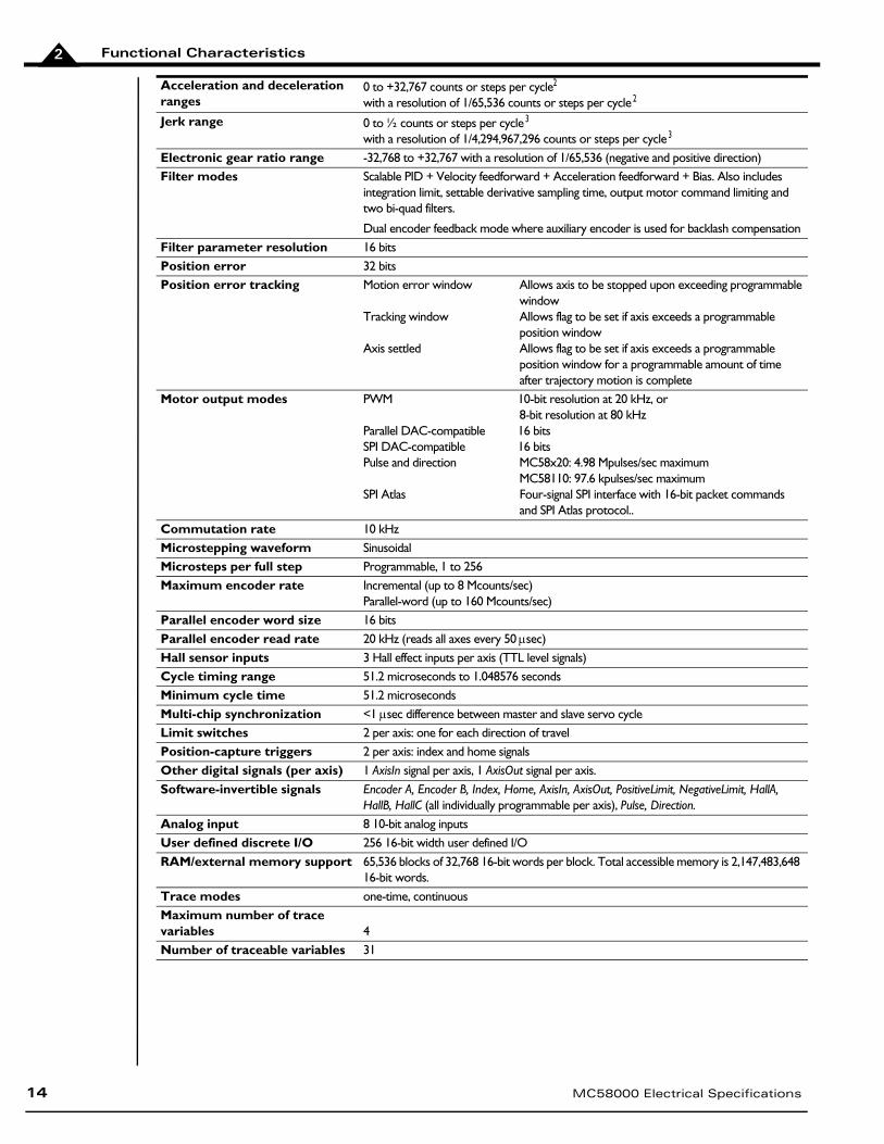
Acceleration and deceleration ranges
0 to +32,767 counts or steps per cycle2
with a resolution of 1/65,536 counts or steps per cycle 2
Jerk range 0 to ½ counts or steps per cycle 3 with a resolution of 1/4,294,967,296 counts or steps per cycle 3
Electronic gear ratio range -32,768 to +32,767 with a resolution of 1/65,536 (negative and positive direction)Filter modes Scalable PID + Velocity feedforward + Acceleration feedforward + Bias. Also includes
integration limit, settable derivative sampling time, output motor command limiting and two bi-quad filters.
Dual encoder feedback mode where auxiliary encoder is used for backlash compensationFilter parameter resolution 16 bitsPosition error 32 bitsPosition error tracking Motion error window Allows axis to be stopped upon exceeding programmable
windowTracking window Allows flag to be set if axis exceeds a programmable
position windowAxis settled Allows flag to be set if axis exceeds a programmable
position window for a programmable amount of timeafter trajectory motion is complete
Motor output modes PWM 10-bit resolution at 20 kHz, or 8-bit resolution at 80 kHz
Parallel DAC-compatible 16 bitsSPI DAC-compatible 16 bitsPulse and direction MC58x20: 4.98 Mpulses/sec maximum
MC58110: 97.6 kpulses/sec maximumSPI Atlas Four-signal SPI interface with 16-bit packet commands
and SPI Atlas protocol..Commutation rate 10 kHzMicrostepping waveform SinusoidalMicrosteps per full step Programmable, 1 to 256Maximum encoder rate Incremental (up to 8 Mcounts/sec)
Parallel-word (up to 160 Mcounts/sec)Parallel encoder word size 16 bitsParallel encoder read rate 20 kHz (reads all axes every 50sec)Hall sensor inputs 3 Hall effect inputs per axis (TTL level signals)Cycle timing range 51.2 microseconds to 1.048576 secondsMinimum cycle time 51.2 microsecondsMulti-chip synchronization <1 sec difference between master and slave servo cycleLimit switches 2 per axis: one for each direction of travelPosition-capture triggers 2 per axis: index and home signalsOther digital signals (per axis) 1 AxisIn signal per axis, 1 AxisOut signal per axis.Software-invertible signals Encoder A, Encoder B, Index, Home, AxisIn, AxisOut, PositiveLimit, NegativeLimit, HallA,
HallB, HallC (all individually programmable per axis), Pulse, Direction.Analog input 8 10-bit analog inputsUser defined discrete I/O 256 16-bit width user defined I/ORAM/external memory support 65,536 blocks of 32,768 16-bit words per block. Total accessible memory is 2,147,483,648
16-bit words.Trace modes one-time, continuousMaximum number of trace variables 4Number of traceable variables 31
14 MC58000 Electrical Specifications

Functional Characteristics 2
2.2 Physical Characteristics and Mounting Dimensions
.
Figure 2-1: CP chip (all dimensions in millimeters)
MC58000 Electrical Specifications 15

Functional Characteristics2
16 MC58000 Electrical Specifications
.
2.3 Absolute Maximum Environmental and Electrical Ratings2.3.1 CP 58110, 58x20
2.3.2 IO 58x20
Supply Voltage (Vcc) -0.3V to +4.6V
Vcc5 range -0.3V to +5.5V
Input voltage (Vi) -0.3V to +4.6V
Package thermal impedance (JA) 32°C/W
Junction temperature range (Tj) -40°C to 150°C
Storage Temperature (Ts) -65°C to 150°C
Nominal Clock Frequency (Fclk) 20.0 MHz
Supply Voltage (Vcc) -0.5V to +3.6V
Input voltage (Vi) -0.5V to Vcc +0.5V
Package thermal impedance (JA) 39.7°C/W
Junction temperature range (Tj) -40°C to 150°C
Storage Temperature (Ts) -65°C to 150°C
Nominal Clock Frequency (Fclk) 40.0 MHz
Figure 2-2: IO Chip (all dimensions in millimeters)
Functional Characteristics 2
MC58000 Electrical Specifications 17
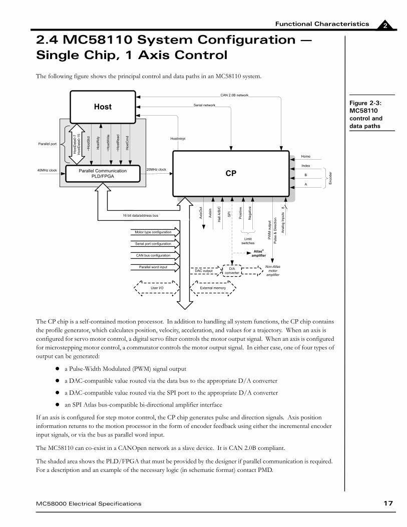
2.4 MC58110 System Configuration — Single Chip, 1 Axis Control
The following figure shows the principal control and data paths in an MC58110 system.
The CP chip is a self-contained motion processor. In addition to handling all system functions, the CP chip contains the profile generator, which calculates position, velocity, acceleration, and values for a trajectory. When an axis is configured for servo motor control, a digital servo filter controls the motor output signal. When an axis is configured for microstepping motor control, a commutator controls the motor output signal. In either case, one of four types of output can be generated:
a Pulse-Width Modulated (PWM) signal output
a DAC-compatible value routed via the data bus to the appropriate D/A converter
a DAC-compatible value routed via the SPI port to the appropriate D/A converter
an SPI Atlas bus-compatible bi-directional amplifier interface
If an axis is configured for step motor control, the CP chip generates pulse and direction signals. Axis position information returns to the motion processor in the form of encoder feedback using either the incremental encoder input signals, or via the bus as parallel word input.
The MC58110 can co-exist in a CANOpen network as a slave device. It is CAN 2.0B compliant.
The shaded area shows the PLD/FPGA that must be provided by the designer if parallel communication is required. For a description and an example of the necessary logic (in schematic format) contact PMD.
Figure 2-3: MC58110 control and data paths
HostIntrpt
Host
CP
Hos
tDat
a0-7
Hos
tDat
a0-1
5
Parallel port
40MHz clock
~Hos
tRea
d
External memoryUser I/O
Parallel CommunicationPLD/FPGA
20MHz clock
16 bit data/address bus Axi
sOut
Neg
ativ
e
Pos
itive
Axi
sIn
Limitswitches
Hal
lA/B
/C
Non-Atlasmotoramplifier
DAC output D/Aconverter
A
Home
Index
B
Enc
oder
Serial network
CAN 2.0B network
SP
I
Serial port configuration
CAN bus configuration
Parallel word input
Motor type configuration Ana
log
Inpu
ts8
PW
Mou
tput
Pul
se&
Dire
ctio
n
Hos
tCm
d
~Hos
tWrit
e
Hos
tRdy
~Hos
tSlc
t
Atlas®
amplifier
Functional Characteristics2
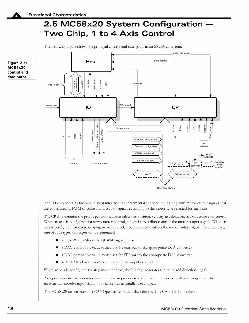
2.5 MC58x20 System Configuration — Two Chip, 1 to 4 Axis Control
The following figure shows the principal control and data paths in an MC58x20 system.
The IO chip contains the parallel host interface, the incremental encoder input along with motor output signals that are configured as PWM or pulse and direction signals according to the motor type selected for each axis.
The CP chip contains the profile generator, which calculates position, velocity, acceleration, and values for a trajectory. When an axis is configured for servo motor control, a digital servo filter controls the motor output signal. When an axis is configured for microstepping motor control, a commutator controls the motor output signal. In either case, one of four types of output can be generated:
a Pulse-Width Modulated (PWM) signal output
a DAC-compatible value routed via the data bus to the appropriate D/A converter
a DAC-compatible value routed via the SPI port to the appropriate D/A converter
an SPI Atlas bus-compatible bi-directional amplifier interface
When an axis is configured for step motor control, the IO chip generates the pulse and direction signals.
Axis position information returns to the motion processor in the form of encoder feedback using either the incremental encoder input signals, or via the bus as parallel word input.
The MC58x20 can co-exist in a CANOpen network as a slave device. It is CAN 2.0B compliant.
Figure 2-4: MC58x20 control and data paths
Host
IO CP
Hos
tDat
a0-7
Hos
tDat
a0-1
5
Parallel port
40MHz clock
HostIntrpt
20MHz clock
Serial network
Axi
sOut
Neg
ativ
e
Pos
itive
Axi
sIn
Limitswitches
A
Hom
e
Inde
x
B
Encoder
External memory
Other user devices
16-bit data bus
User I/O
Serial port configuration
CAN bus configuration
Parallel word input
Hal
lA/B
/C
CAN 2.0B network
SP
I
Motor type configuration
Pul
se/P
WM
Dire
ctio
n/S
PIE
nabl
e/ P
WM
AtR
est /
PW
M
To Motor Amplifier
Ana
log
Inpu
ts8
~Hos
tRea
d
Hos
tCm
d
~Hos
tWrit
e
Hos
tRdy
~Hos
tSlc
t
DAC output D/Aconverter
Atlas®
amplifier
Non-Atlasmotoramplifier
18 MC58000 Electrical Specifications
3
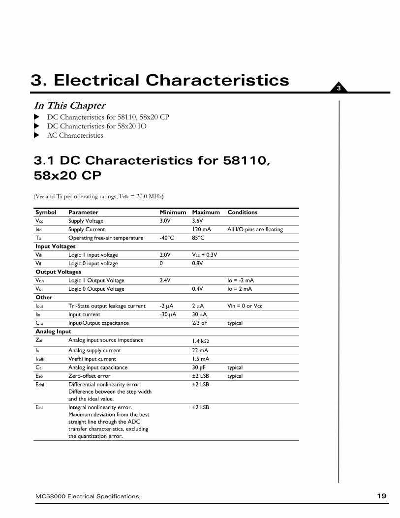
3. Electrical Characteristics In This ChapterDC Characteristics for 58110, 58x20 CPDC Characteristics for 58x20 IOAC Characteristics3.1 DC Characteristics for 58110, 58x20 CP
(Vcc and Ta per operating ratings, Fclk = 20.0 MHz)
Symbol Parameter Minimum Maximum ConditionsVcc Supply Voltage 3.0V 3.6VIdd Supply Current 120 mA All I/O pins are floatingTa Operating free-air temperature -40°C 85°CInput VoltagesVih Logic 1 input voltage 2.0V Vcc + 0.3VVil Logic 0 input voltage 0 0.8VOutput VoltagesVoh Logic 1 Output Voltage 2.4V Io = -2 mAVol Logic 0 Output Voltage 0.4V Io = 2 mAOtherIout Tri-State output leakage current -2 A 2 A Vin = 0 or VccIin Input current -30 A 30 ACio Input/Output capacitance 2/3 pF typicalAnalog InputZai Analog input source impedance 1.4 k
Ia Analog supply current 22 mAIrefhi Vrefhi input current 1.5 mACai Analog input capacitance 30 pF typicalEzo Zero-offset error ±2 LSB typicalEdnl Differential nonlinearity error.
Difference between the step width and the ideal value.
±2 LSB
Einl Integral nonlinearity error. Maximum deviation from the best straight line through the ADC transfer characteristics, excluding the quantization error.
±2 LSB
MC58000 Electrical Specifications 19
Electrical Characteristics3
3.2 DC Characteristics for 58x20 IO
(Vcc and Ta per operating ratings, Fclk = 40.0 MHz)
3.3 AC CharacteristicsSee timing diagrams in Chapter 4, “I/O Timing Diagrams,” for Tn numbers. The symbol “~” indicates active low signal.
Symbol Parameter Minimum Maximum ConditionsVcc Supply Voltage 3.0V 3.6VIdd Supply Current 24 mA All I/O pins are floatingTa Operating free-air temperature -40°C 85°CInput VoltagesVih Logic 1 input voltage 2.0V VccVil Logic 0 input voltage 0 0.8VOutput VoltagesVoh Logic 1 Output Voltage 2.4V Io = -2 mAVol Logic 0 Output Voltage 0.4V Io = 6 mAOtherIout Tri-State output leakage current -10 A 10 AIin Input current -10 A 10 ACio Input/Output capacitance 7/7 pF typical
Timing Interval Tn Minimum MaximumClock
IOClkIn Frequency (Fclk)1 8 MHz 40 MHz
IOClkIn pulse duration3 T1a 0.4 T2a 0.6 T2a
IOClkIn Period T2a 25 nsec 125 nsec
CPClkIn Frequency (Fclk)1 4 MHz 20 MHz
CPClkIn pulse duration3 T1b 0.4 T2b 0.6 T2b
CPClkIn Period T2b 50 nsec 250 nsecCPClkIn rise/fall time T58 5 nsecEncoderEncoder Pulse Width T3 200 nsecDwell Time Per State T4 100 nsecIndex Setup and Hold (relative to Quad A and Quad B low) T5 0 nsecHost IO~HostSlct Hold Time T6 0 nsec~HostSlct Setup Time T7 0 nsecHostCmd Setup Time T8 0 nsecHostCmd Hold Time T9 0 nsecRead Data Access Time T10 25 nsecRead Data Hold Time T11 10 nsec~HostRead High to HI-Z Time T12 20 nsecHostRdy Hold Time T13 40 nsec 70 nsec~HostWrite Pulse Width T14 70 nsecWrite Data Delay Time T15 15 nsecWrite Data Hold Time T16 0 nsec
Read Recovery Time2 T17 60 nsec
Write Recovery Time2 T18 60 nsec
~HostRead Pulse Width T19 70 nsec
20 MC58000 Electrical Specifications

Electrical Characteristics 3
MC58000 Electrical Specifications 21
External Memory Read ClockOut low to control valid T20 4 nsecClockOut low to address valid T21 8 nsecAddress valid to ~ReadEnable low T22 5.5 nsecClockOut high to ~ReadEnable low T23 5 nsecClockOut low to ~ReadEnable high T23a -8 nsec 1 nsecData access time from Address valid T24 40 nsecData access time from ~ReadEnable low T25 31 nsecData setup time before ~ReadEnable high T25a 8 nsecData hold time after ~ReadEnable high T26 0 nsec~ReadEnable high to Address invalid T26a 0 nsecClockOut low to control inactive T27 5 nsecAddress hold time after ClockOut low T28 2 nsecClockOut low to Strobe low T29 5 nsecClockOut low to Strobe high T30 6 nsecW/~R low to R/~W rising delay time T31 5 nsecExternal Memory Write ClockOut high to control valid T32 4 nsecClockOut high to address valid T33 10 nsecAddress valid to ~WriteEnable low T34 3.5 nsecClockOut low to ~WriteEnable low T35 6 nsecClockOut low to ~WriteEnable high T35a 6 nsecData setup time before ~WriteEnable high T36 33 nsecData bus driven from ClockOut low T37 -3 nsecData hold time after ~WriteEnable high T38 2 nsecClockOut high to control inactive T39 5 nsecAddress hold time after ClockOut low T40 -5 nsecClockOut low to Strobe low T41 6 nsecClockOut low to Strobe high T42 6 nsecR/~W low to W/~R rising delay time T43 5 nsecClockOut high to control valid T44 6 nsecClockOut high to R/~W high T44a 6 nsecPeripheral Device Read
ClockOut high to ClockOut low4 T45 112.5 nsec 562.5 nsec
Data access time from Address valid T46 65 nsecData access time from ~ReadEnable low T47 56 nsecPeripheral Device Write
ClockOut low to ClockOut low4 T48 125 nsec 625 nsec
Data setup time before ~WriteEnable high T49 58 nsecDevice ResetReset low pulse width T50 400 nsecDevice Ready/ Outputs Initialized T57 1.5 msec1. Performance figures and timing information valid at Fclk = 40.0 MHz for the dual chip configuration and Fclk =
20.0 MHz for the single chip configurations only. For timing information and performance parameters at lower Fclk, see Section 6.2.3, “Using a Non-standard System Clock Frequency.”
2. For 8/16 interface modes only.3. The clock low/high split has an allowable range of 40 - 60%.4. The minimum and maximum values correspond to a 50 nsec and 250 nsec CPClkIn clock periods, or 25 nsec
and 125 nsec IOClkIn clock periods, respectively.
Timing Interval Tn Minimum Maximum

Electrical Characteristics
22 MC58000 Electrical Specifications
3
This page intentionally left blank.
4
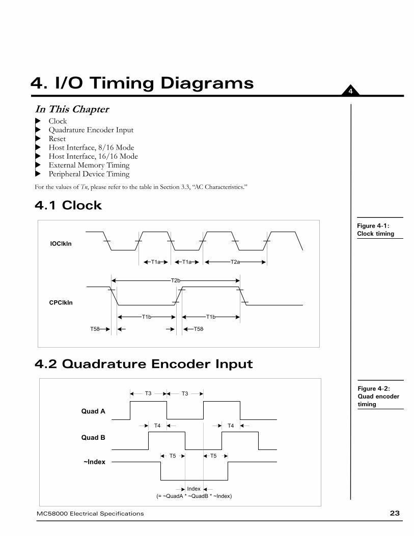
4. I/O Timing DiagramsMC58000 Electrical Specifications 23
In This ChapterClockQuadrature Encoder InputResetHost Interface, 8/16 ModeHost Interface, 16/16 ModeExternal Memory TimingPeripheral Device Timing
For the values of Tn, please refer to the table in Section 3.3, “AC Characteristics.”
4.1 Clock
4.2 Quadrature Encoder Input
IOClkIn
CPClkIn
T2aT1aT1a
T58T58
T1b T1b
T2b
Figure 4-1: Clock timing
Figure 4-2: Quad encoder timing
Quad A
Quad B
T3 T3
T4 T4
T5
(= ~QuadA * ~QuadB * ~Index)
~IndexT5
Index
I/O Timing Diagrams4
4.3 Reset
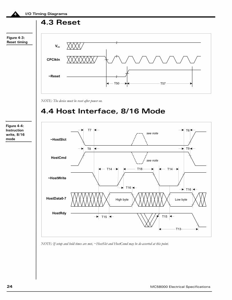
NOTE: The device must be reset after power on.
4.4 Host Interface, 8/16 Mode
NOTE: If setup and hold times are met, ~HostSlct and HostComd may be de-asserted at this point.
Figure 4-3: Reset timing
Vcc
CPClkIn
~Reset
T50 T57
Figure 4-4: Instruction write, 8/16 mode
HostData0-7
~HostSlct
HostCmd
HostRdy
~HostWrite
T7 T6see note
T8
T18
T9
T14T14
see note
T16T16
T15 T15
Low byteHigh byte
T13
24 MC58000 Electrical Specifications

I/O Timing Diagrams 4
MC58000 Electrical Specifications 25
NOTE: If setup and hold times are met, ~HostSlct and HostComd may be de-asserted at this point.
NOTE: If setup and hold times are met, ~HostSlct and HostComd may be de-asserted at this point.
Figure 4-5: Data write, 8/16 mode
HostData0-7
~HostSlct
HostCmd
HostRdy
~HostWrite
T7
T8
T6
T9
T15
see note
see note
Low byte
T16T16
T15
High byte
T18 T14T14
T13
Figure 4-6: Data read, 8/16 mode
HostData0-7
~HostSlctT7
T8
T6
T9
T12
T11
HostCmd
HostRdy
~HostRead
T12
T10
High-Z High-Z High-ZHighbyte
Low byte
see note
see note
T19 T19
T17
T13
I/O Timing Diagrams4
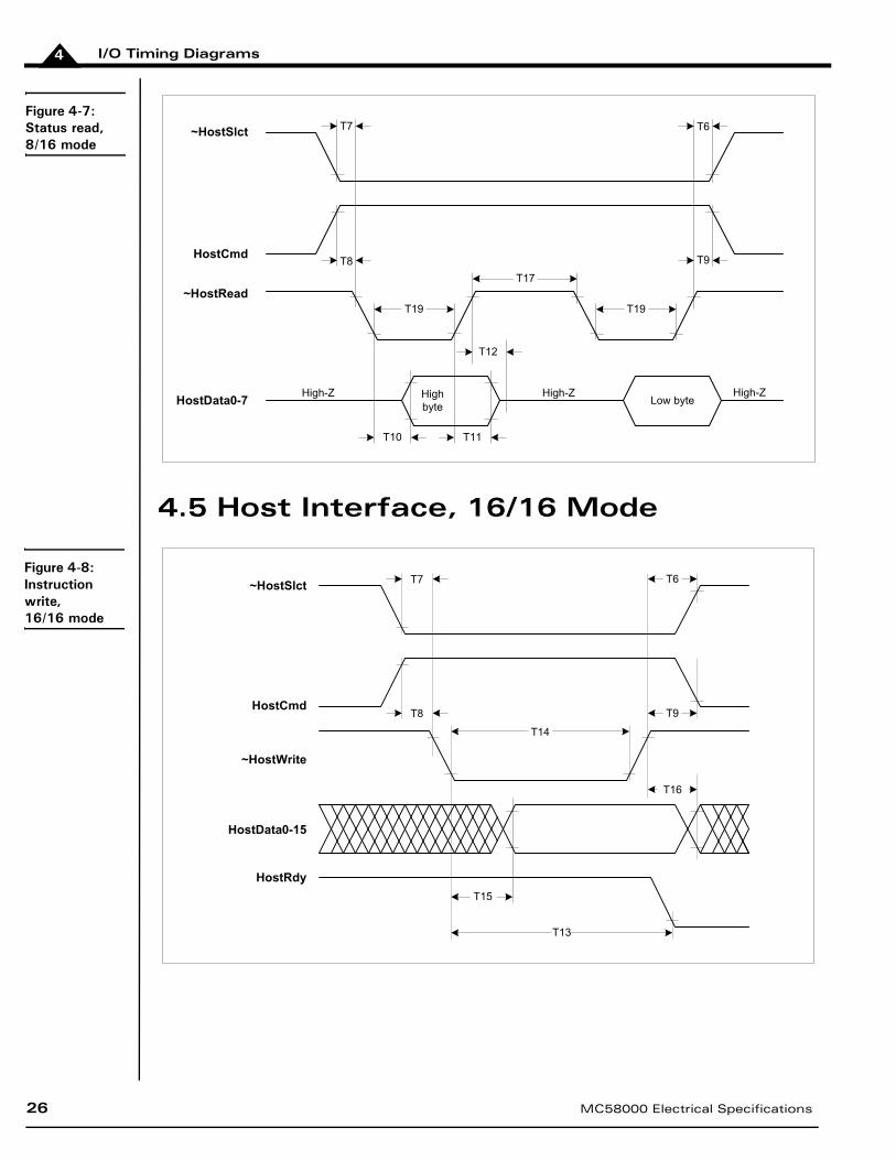
4.5 Host Interface, 16/16 Mode
Figure 4-7: Status read, 8/16 mode
~HostSlct T7
T8
T17
T6
T9
T11
HostCmd
HostData0-7
~HostRead
T12
T10
High-Z High-Z High-ZHighbyte
Low byte
T19 T19
Figure 4-8: Instruction write, 16/16 mode
T7 T6
T9
T14
T16
T8
T15
~HostSlct
HostCmd
~HostWrite
HostData0-15
HostRdy
T13
26 MC58000 Electrical Specifications

I/O Timing Diagrams 4
Figure 4-9: Data write, 16/16 mode
T7 T6
T9
T14
T16
T8
T15
~HostSlct
HostCmd
~HostWrite
HostData0-15
HostRdy
T13
Figure 4-10: Data read, 16/16 mode
~HostSlctT7
T8
T11
HostCmd
HostData0-15
HostRdy
~HostRead
T10
High-Z High-Z
T6
T9
T19
T12
T13
MC58000 Electrical Specifications 27
I/O Timing Diagrams4
28 MC58000 Electrical Specifications
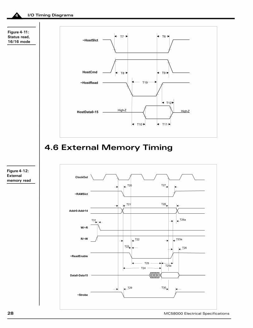
4.6 External Memory Timing
Figure 4-11: Status read, 16/16 mode ~HostSlct
T7
T8
T11
HostCmd
HostData0-15
~HostRead
T12
T10
High-Z High-Z
T6
T9
T19
Figure 4-12: External memory read
~RAMSlct
Addr0-Addr14
~ReadEnable
Data0-Data15
T24
T20
~Strobe
ClockOut
T21
T27
T30 T29
T22
T25
T26
T28
T23
W/~R
R/~W
T31
T23a
T26a
T25a
I/O Timing Diagrams 4
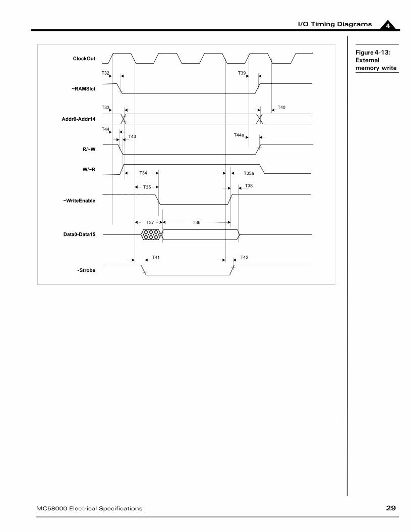
Figure 4-13: External memory write
~RAMSlct
Addr0-Addr14
R/~W
~WriteEnable
Data0-Data15
T36
T32
~Strobe
W/~R
ClockOut
T33
T43
T39
T42 T41
T34
T38
T40
T35
T37
T44
T35a
T44a
MC58000 Electrical Specifications 29

I/O Timing Diagrams4
4.7 Peripheral Device Timing
Figure 4-14: Peripheral device read
~PeriphSlct
Addr0-Addr15
~ReadEnable
Data0-Data15
T20
~Strobe
ClockOut
T21
T27
T30T29
T22
T26
T28
T23
W/~R
R/~W
T31
T23a
T47
T46
T45 T26a
T25a
30 MC58000 Electrical Specifications
I/O Timing Diagrams
MC58000 Electrical Specifications 31
4
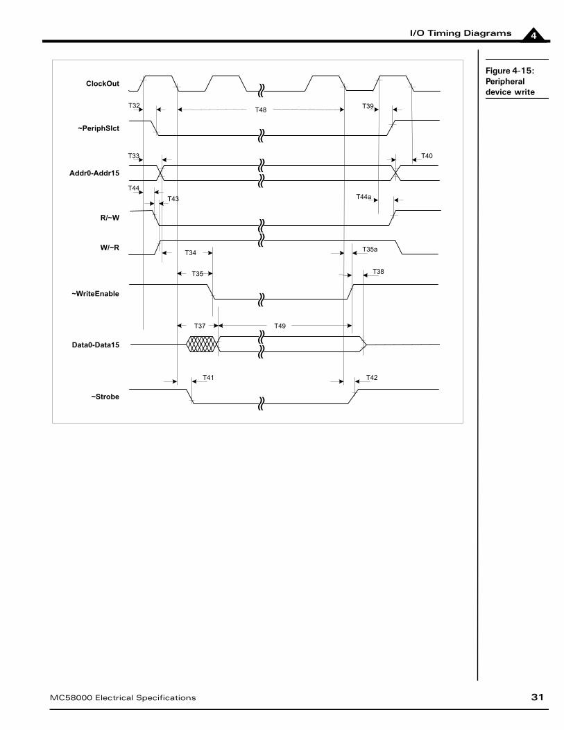
Figure 4-15: Peripheral device write
~PeriphSlct
Addr0-Addr15
R/~W
~WriteEnable
Data0-Data15
T32
~Strobe
W/~R
ClockOut
T33
T43
T39
T42 T41
T34
T38
T40
T35
T37
T44
T35a
T44a
T49
T48

I/O Timing Diagrams
32 MC58000 Electrical Specifications
4
This page intentionally left blank.
5
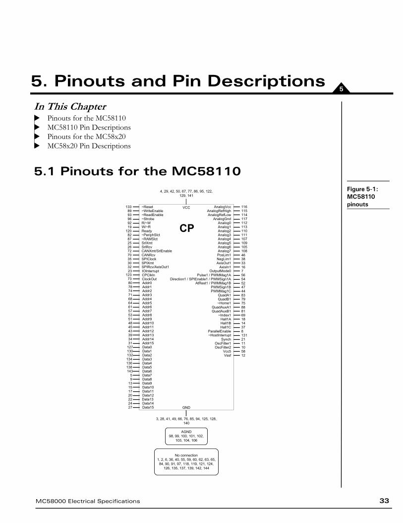
5. Pinouts and Pin Descriptions In This ChapterPinouts for the MC58110MC58110 Pin DescriptionsPinouts for the MC58x20MC58x20 Pin Descriptions5.1 Pinouts for the MC58110Figure 5-1: MC58110 pinouts
~ReadEnable
~PeriphSlct
127130132134136138143
59
13151720222427
80787471686461575351484543393431
25267270
123
SrlXmtSrlRcvCANXmt/SrlEnableCANRcv
CPClkIn
Data0Data1Data2Data3Data4Data5Data6Data7Data8Data9Data10Data11Data12Data13Data14Data15
Addr0Addr1Addr2Addr3Addr4Addr5Addr6Addr7Addr8Addr9Addr10Addr11Addr12Addr13Addr14Addr15
92
1208287
133
R/~W
Ready
~RAMSlct
~Reset
19
93
4638
PosLim1NegLim1
115114117
3316
AxisOut1AxisIn1
AnalogVccAnalogRefHighAnalogRefLow
AnalogGnd
116
Hall1AHall1BHall1C
181437
W/~R
~HostInterrupt 131Synch 21
Vssf 12
OscFilter1 11OscFilter2 10
Vcc5 58
VCC
4, 29, 42, 50, 67, 77, 86, 95, 122, 129, 141
112113110111107109105108
Analog0Analog1Analog2Analog3Analog4Analog5Analog6Analog7
3530
SPIClockSPIXmt
GND
3, 28, 41, 49, 66, 76, 85, 94, 125, 128, 140
No connection1, 2, 6, 36, 40, 55, 59, 60, 62, 63, 65, 84, 90, 91, 97, 118, 119, 121, 124,
126, 135, 137, 139, 142, 144
AGND98, 99, 100, 101, 102,
103, 104, 106
73 ClockOut
96 ~Strobe
~WriteEnable89
23 IOInterrupt
5247
AtRest1 / PWMMag1BPWMSign1B
44PWMMag1C
5654
Pulse1 / PWMMag1ADirection1 / SPIEnable1 / PWMSign1A
8379
QuadA1QuadB1
ParallelEnable 8
69~Index1
8881
QuadAuxA1QuadAuxB1
75~Home1
CP
32 SPIRcv/AxisOut17OutputMode0
MC58000 Electrical Specifications 33

Pinouts and Pin Descriptions5
34 MC58000 Electrical Specifications
5.2 MC58110 Pin Descriptions58110 CP
Pin Name and Number Direction Description
~Reset 133 input/output This is the master reset signal. This pin must be brought low to reset the chipset to its initial condition. NOTE: A software reset will momentarily drive this pin low.
~WriteEnable 89 output This signal is the write-enable strobe. When low, this signal indicates that data is being written to the bus.
~ReadEnable 93 output This signal is the read-enable strobe. When low, this signal indicates that data is being read from the bus.
~Strobe 96 output This signal is low when the data and address are valid during CP communications.
R/~W 92 output This signal is high when the CP chip is performing a read, and low when it is performing a write.
W/~R 19 output This signal is the inverse of R/~W; it is high when R/~W is low, and vice versa. For some decode circuits and devices this is more convenient than R/~W.
Ready 120 input Ready can be pulled low to add wait states for external accesses. Ready indicates that an external device is prepared for a bus transaction to be completed. If the device is not ready, it pulls the Ready pin low. The motion processor then waits one cycle and checks Ready again.
This signal may remain unconnected if it is not used.
~PeriphSlct 82 output This signal is low when peripheral devices on the data bus are being addressed.
~RAMSlct 87 output This signal is low when external memory is being accessed.
SrlXmt 25 output This pin outputs serial data from the asynchronous serial port.
SrlRcv 26 input This pin inputs serial data to the asynchronous serial port. If not used, this pin should be tied to Vcc.
CANXmt/SrlEnable
72 output When the CAN host interface is used, this pin transmits serial data to the CAN transceiver. When the multi-drop serial interface is used, this pin sets the serial port enable line and the CANXmt function is not available. SrlEnable is high during transmission for the multi-drop protocol and always high during point–point mode.
CANRcv 70 input This pin receives serial data from the CAN transceiver. If not used, this pin should be tied to Vcc.
SPIClock 35 output This pin is the clock signal used for strobing synchronous serial data on the SPI bus to DACs or to Atlas amplifiers. This signal is only active when SPI data is being transmitted.
SPIXmt 30 output This pin transmits synchronous serial data on the SPI bus to DACs or to Atlas amplifiers.
SPIRcv/AxisOut1
32 input or output If OutputMode0 is low at powerup this pin serves as the SPIRcv input, used with the SPI Atlas amplifier interface.If OutputMode0 is left floating at powerup this pin provides the AxisOut1 output. AxisOut1 can be programmed to track the state of any bit in the status registers.
If this pin is not used, it may remain unconnected.
IOInterrupt 23 input This interrupt signal is used for IO to CP communication.
This signal may remain unconnected if it is not used.
CPClkIn 123 input This is the clock signal for the motion processor. It is driven at a nominal 20 MHz.
ClockOut 73 output This signal is the reference output clock. Its frequency is twice the frequency of the input clock (which is normally 20 MHz), resulting in a nominal output frequency of 40 MHz. ClockOut will not be active when ~Reset is active.

Pinouts and Pin Descriptions 5
Addr0Addr1Addr2Addr3Addr4Addr5Addr6Addr7Addr8Addr9Addr10Addr11Addr12Addr13Addr14Addr15
80787471686461575351484543393431
output Multi-purpose address lines. These pins comprise the CP chip’s external address bus, which is used to select devices for communication over the data bus.
Other address pins may be used for DAC output, parallel word input, external memory, or user-defined I/O operations. See Section 6.3, “Peripheral Device Address Map,” for a complete memory map.
Data0Data1Data2Data3Data4Data5Data6Data7Data8Data9Data10Data11Data12Data13Data14Data15
1271301321341361381435913151720222427
bi-directional Multi-purpose data lines. These pins comprise the CP chip’s external data bus, which is used for all communications with peripheral devices such as external memory or DACs. They may also be used for parallel-word input and for user-defined I/O operations.
AnalogVcc 116 input Analog input Vcc. This pin should be connected to the analog input supply voltage, which must be in the range of 3.0V to 3.6V.
If the analog input circuitry is not used, this pin should be tied to Vcc.
AnalogRefHigh 115 input Analog high voltage reference for A/D input. The allowed range is AnalogRefLow to AnalogVcc.
If the analog input circuitry is not used, this pin should be tied to Vcc.
AnalogRefLow 114 input Analog low voltage reference for A/D input. The allowed range is AnalogGND to AnalogRefHigh.
If the analog input circuitry is not used, this pin should be tied to GND.
AnalogGND 117 input Analog input ground. This pin should be connected to the analog input power supply return.
If the analog input circuitry is not used, this pin should be tied to GND.
Analog0Analog1Analog2Analog3Analog4Analog5Analog6Analog7
112113110111107109105108
input These signals provide general-purpose analog voltage levels which are sampled by an internal A/D converter. The A/D resolution is 10 bits.
The allowed signal input range is AnalogRefLow to AnalogRefHigh.
Any unused pins should be tied to AnalogGND.
If the analog input circuitry is not used, these pins should be tied to GND.
58110 CPPin Name and Number Direction Description
MC58000 Electrical Specifications 35

Pinouts and Pin Descriptions5
PosLim1 46 input This signal provides input from the positive-side (forward) travel limit switch. On power-up or after reset, this signal defaults to active low interpretation, but the interpretation can be set to active high interpretation using the SetSignalSense instruction.
If this pin is not used, it may remain unconnected.
NegLim1 38 input This signal provides input from the negative-side (reverse) travel limit switch. On power-up or after reset, this signal defaults to active low interpretation, but the interpretation can be set to active high interpretation using the SetSignalSense instruction.
If this pin is not used, it may remain unconnected.
AxisOut1 33 output For Magellan ICs revision 3.0 or higher this pin provides the AxisOut1 output. AxisOut1 can be programmed to track the state of any bit in the status registers.
AxisIn1 16 input This pin is a general-purpose input which can also be used as a breakpoint input.
If this pin is not used, it may remain unconnected.OutputMode0 7 input OutputMode0 should be tied low when SPI Atlas interfacing will be used, and with
Magellan ICs revision 3.0 or higher. For Magellan ICs lower than revision 3.0 this pin should be left floating. The state of this pin is only checked during power up.
PWMMag1A/Pulse1
PWMSign1A/Direction1/SPIEnable1
AtRest1/PWMMag1B
PWMSign1B
PWMMag1C
56
54
52
47
44
output Depending upon the selected motor type and output mode, these signals have the following functions:
PWMMag encodes the magnitude of the pulse width modulated output.
PWMSign signals encode the sign of the pulse width modulated output.
In 2- or 3-phase PWM 50/50 mode, PWMMag1A/1B/1C are the only signals, and encode both magnitude and direction in one signal.
In single-phase PWM sign/magnitude mode, PWMMag1A and PWMSign1A are the PWM magnitude and direction signals respectively.
In 2-phase PWM sign/magnitude mode, PWMMag1A and PWMSign1A are the PWM magnitude and direction signals for Phase A. PWMMag1B and PWMMag1B are the PWM magnitude and direction signals for Phase B.
SPIEnable provides the enable signal when SPIDAC or SPI Atlas motor output mode is used. This signal is active high for SPI DAC, meaning this signal is high when the SPI DAC channel is being written to, and low at all other times. This signal is active low for SPI Atlas mode, meaning it is low when an SPI Atlas communication is occurring, and high at all other times.
For SPI DAC output, SPI output can only be used when the axis being controlled is DC brushed, or when the amplifier expects a single-phase input and it performs brushless motor commutation. For SPI Atlas interfacing, DC Brush, Brushless DC, and step motors are supported.
Pulse provides the pulse (step) signal to the motor. A step occurs when the signal transitions from a high state to a low state. This default behavior can be changed from a low to a high state transition using the command SetSignalSense.
Direction indicates the direction of motion, and works in conjunction with the pulse signal. A high level on this signal indicates a positive direction move, and a low level indicates a negative direction move.
AtRest indicates that the axis is at rest, and that the step motor can be switched to low power or standby. A high level on this signal indicates the axis is at rest. A low signal indicates the axis is in motion.
Refer to the Motor Interfacing section of the Magellan Motion Processor User’s Guide for more information on PWM encoding schemes.
58110 CPPin Name and Number Direction Description
36 MC58000 Electrical Specifications
Pinouts and Pin Descriptions 5
QuadA1QuadB1
8379
input These pins should be connected to the A and B quadrature signals from the incremental encoder. When the axis is moving in the positive (forward) direction, signal A leads signal B by 90°.
NOTE: Some encoders require a pull-up resistor to 3.3V on each signal to establish a proper high signal. Check your encoder’s electrical specification.
If these pins are not used, they may remain unconnected.~Home1 75 input This pin provides the home signal; a general-purpose input to the position capture
mechanism. A valid home signal is recognized by the motion processor when ~Home transitions from high to low.
If this pin is not used, it may remain unconnected.QuadAuxA1QuadAuxB1~Index1
888169
input If index capture is required, the encoder A and B signals connected to QuadA1 and QuadB1 signals must also be connected to QuadAuxA1 and QuadAuxB1.
The index pin should be connected to the index signal from the incremental encoder. A valid index pulse is recognized by the motion processor when it meets the criteria shown in Figure 4-2.
If these pins are not used, they may remain unconnected.
WARNING! There is no internal gating of the index signal with the encoder A and B inputs. This must be performed externally if desired.
Hall1AHall1BHall1C
181437
input Hall sensor inputs. These signals encode six valid states as follows: A on, A and B on, B on, B and C on, C on, C and A on. A sensor is defined as being on when its signal is high. On power-up or after reset, these signals default to active high interpretation, but the interpretation can be set to active low interpretation using the SetSignalSense instruction.
If these pins are not used, they may remain unconnected.
ParallelEnable 8 input This signal enables/disables the parallel communication with the host. If this signal is tied high, the parallel interface is enabled. If this signal is tied low, the parallel interface is disabled. Contact PMD for more information on parallel communication.
WARNING! This signal should only be tied high if an external logic device which implements the parallel communication logic is included in the design.
~HostInterrupt 131 output When low, this signal causes an interrupt to be sent to the host processor.
Synch 21 input/output This pin is the synchronization signal. In the disabled mode, the pin is configured as an input and is not used. In the master mode, the pin outputs a synchronization pulse that can be used by slave nodes or other devices to synchronize with the internal chip cycle of the master node. In the slave mode, the pin is configured as an input and should be connected to the Synch pin on the master node. This signal is falling edge triggered. A pulse on the pin synchronizes the internal chip cycle to the signal provided by the master node.
If this pin is not used, it may remain unconnected.
OscFilter1OscFilter2
1110
These signals connect to the external oscillator filter circuitry. Section 6.6.5, “External Oscillator Filter,” details the required filter circuitry.
Vcc5 58 This signal can be tied to a 5V supply if available. If 5V is not available this signal must be tied to GND. Being tied to GND will not adversely affect the device performance.
Vssf 12 This signal must be tied to Vcc. It must also be tied to pin 28 via a bypass capacitor. A ceramic capacitor with a value between 0.1F and 0.01F should be used.
Vcc 4, 29, 42, 50, 67, 77, 86, 95, 122, 129, 141
CP digital supply voltage. All of these pins must be connected to the supply voltage. Vcc must be in the range of 3.0V to 3.6V.
58110 CPPin Name and Number Direction Description
MC58000 Electrical Specifications 37
Pinouts and Pin Descriptions5
GND 3, 28, 41, 49, 66, 76, 85, 94, 125, 128, 140
CP digital supply ground. All of these pins must be connected to the digital power supply return.
AGND 98, 99, 100, 101, 102, 103, 104, 106
These signals must be tied to AnalogGND.
If the analog input circuitry is not used, these pins must be tied to GND.
No connection 1, 2, 6, 36, 40, 55, 59, 60, 62, 63, 65, 84, 90, 91, 97, 118, 119, 121, 124, 126, 135, 137, 139, 142, 144
These signals must remain unconnected.
58110 CPPin Name and Number Direction Description
38 MC58000 Electrical Specifications

Pinouts and Pin Descriptions 5
5.2.1 MC58110 Pin Assignments for Multiple Motor Types
The MC58110 chip supports the output of PWM motor commands in sign/magnitude and 50/50 modes. It can also output pulse and direction signals. The CP chip assigns pin function according to the selected output mode.
If the output mode is set to PWM sign/magnitude, the following pinout should be used.
If the output mode is set to PWM 50/50, the following pinout should be used.
If the output mode is set to Pulse and direction, the following pinout should be used.
If the output mode is set to SPI DAC, the following pinout should be used.
If the output mode is set for SPI Atlas, which is the interface used with PMD's Atlas Digital Amplifiers, the following pinouts should be used.
PWMMag1APWMMag1B
5652
output These pins provide the Pulse Width Modulated signal to the motor. In PWM 50/50 mode, this is the only signal. In PWM sign-magnitude mode, this is the magnitude signal.
PWMSign1APWMSign1B
5447
output In PWM sign-magnitude mode, these pins provide the sign (direction) of the PWM signal to the motor amplifier.
PWMMag1APWMMag1BPWMMag1C
565244
output These pins provide the Pulse Width Modulated signals for each phase to the motor. If the number of phases is two, only phase A and B are valid. If the number of phases is three, phases A, B, and C are valid. The number of phases is set using the command SetMotorType.
In PWM 50/50 mode, these are the only signals.
Pulse1 56 output This pin provides the pulse (step) signal to the motor.
Direction1 54 output This pin indicates the direction of motion, and works in conjunction with the pulse signal.
AtRest1 52 output This signal indicates the axis is at rest, and that the step motor can be switched to low power or standby mode.
SPIEnable1 54 output This pin provides the enable signal when SPI DAC output is active.
SPIClock 35 output This pin provides the SPI Clock signal.
SPIXmt 30 output This pin holds the transmitted SPI data.
OutputMode0 7 input This pin should be tied to ground.
SPIClock 35 output This pin provides the SPI Clock signal.
SPIXmt 30 output This pin holds the transmitted SPI data sent to Atlas.
SPIRcv 32 input This pins holds the received SPI data sent by Atlas.
SPIEnable1 54 output This pin provides the enable signal when SPI Atlas transmissions are active.
MC58000 Electrical Specifications 39
Pinouts and Pin Descriptions5
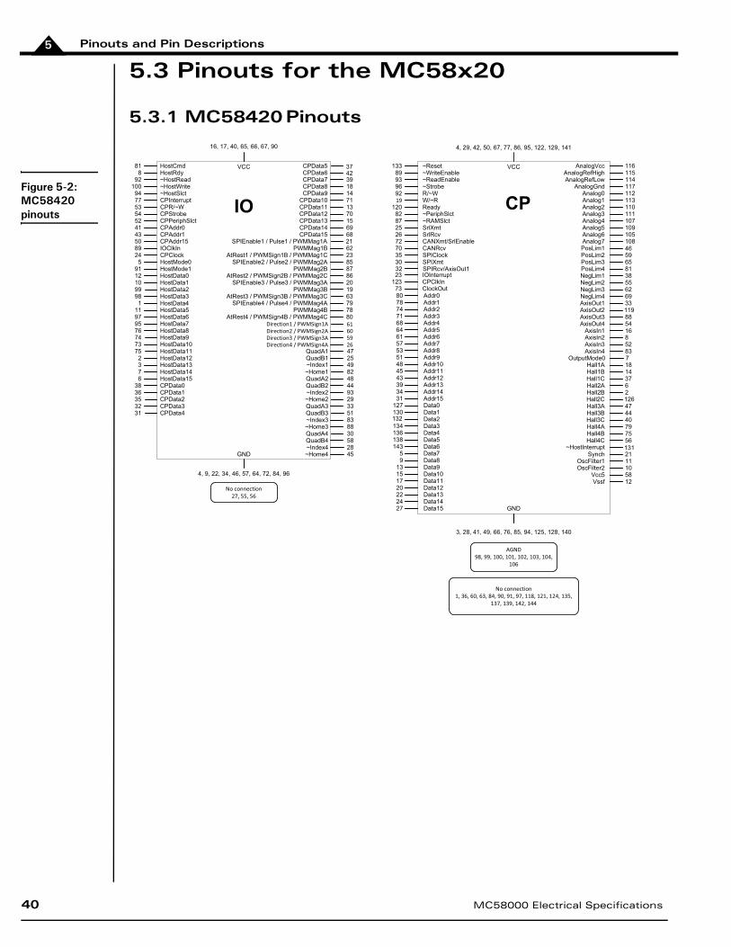
5.3 Pinouts for the MC58x20
5.3.1 MC58420 Pinouts
Figure 5-2: MC58420 pinouts
VCC
16, 17, 40, 65, 66, 67, 90
~ReadEnable
~PeriphSlct
818
92100
94CPData8CPData9
CPData10CPData11CPData12CPData13CPData14CPData15
HostCmdHostRdy~HostRead~HostWrite~HostSlct
121099981
119795767473752376
3836353231
374239
HostData0HostData1HostData2HostData3HostData4HostData5HostData6HostData7HostData8HostData9HostData10HostData11HostData12HostData13HostData14HostData15CPData0CPData1CPData2CPData3CPData4
CPData5CPData6CPData7
181471137015696821
85
20
79
7753545241435089245
91
SPIEnable1 / Pulse1 / PWMMag1A
SPIEnable2 / Pulse2 / PWMMag2A
SPIEnable3 / Pulse3 / PWMMag3A
SPIEnable4 / Pulse4 / PWMMag4A
CPInterruptCPR/~WCPStrobeCPPeriphSlctCPAddr0CPAddr1CPAddr15
CPClockIOClkIn
HostMode0HostMode1
47254982484493293351838830582845
QuadA1QuadB1~Index1~Home1QuadA2QuadB2~Index2~Home2QuadA3QuadB3~Index3~Home3QuadA4QuadB4~Index4~Home4
127130132134136138143
59
13151720222427
80787471686461575351484543393431
25267270
23123
SrlXmtSrlRcvCANXmt/SrlEnableCANRcv
IOInterruptCPClkIn
Data0Data1Data2Data3Data4Data5Data6Data7Data8Data9Data10Data11Data12Data13Data14Data15
Addr0Addr1Addr2Addr3Addr4Addr5Addr6Addr7Addr8Addr9Addr10Addr11Addr12Addr13Addr14Addr15
92
1208287
133
R/~W
Ready
~RAMSlct
~Reset
19
93
4659658138556269
PosLim1PosLim2PosLim3PosLim4NegLim1NegLim2NegLim3NegLim4
115114117
3311988541685283
AxisOut1AxisOut2AxisOut3AxisOut4
AxisIn1AxisIn2AxisIn3AxisIn4
AnalogVccAnalogRefHighAnalogRefLow
AnalogGnd
116
Hall1A
Hall2A
Hall3A
Hall4A
Hall1BHall1C
Hall2CHall2B
Hall3CHall3B
Hall4BHall4C
6
181437
21264744
56
7975
40
PWMMag1BAtRest1 / PWMSign1B / PWMMag1C
PWMMag2BAtRest2 / PWMSign2B / PWMMag2C
PWMMag3BAtRest3 / PWMSign3B / PWMMag3C
PWMMag4BAtRest4 / PWMSign4B / PWMMag4C
2362
8786
1963
7880
59
61
26
Direction1 / PWMSign1A
Direction4 / PWMSign4ADirection3 / PWMSign3ADirection2 / PWMSign2A 60
W/~R
~HostInterrupt 131Synch 21
Vssf 12
OscFilter1 11OscFilter2 10
Vcc5 58
VCC
4, 29, 42, 50, 67, 77, 86, 95, 122, 129, 141
112113110111107109105108
Analog0Analog1Analog2Analog3Analog4Analog5Analog6Analog7
3530
SPIClockSPIXmt
GND
3, 28, 41, 49, 66, 76, 85, 94, 125, 128, 140
No connection1, 36, 60, 63, 84, 90, 91, 97, 118, 121, 124, 135,
137, 139, 142, 144
GND
4, 9, 22, 34, 46, 57, 64, 72, 84, 96
No connection27, 55, 56
AGND98, 99, 100, 101, 102, 103, 104,
106
73 ClockOut
96 ~Strobe
~WriteEnable89
IO CP
32 SPIRcv/AxisOut1
7OutputMode0
40 MC58000 Electrical Specifications
Pinouts and Pin Descriptions 5
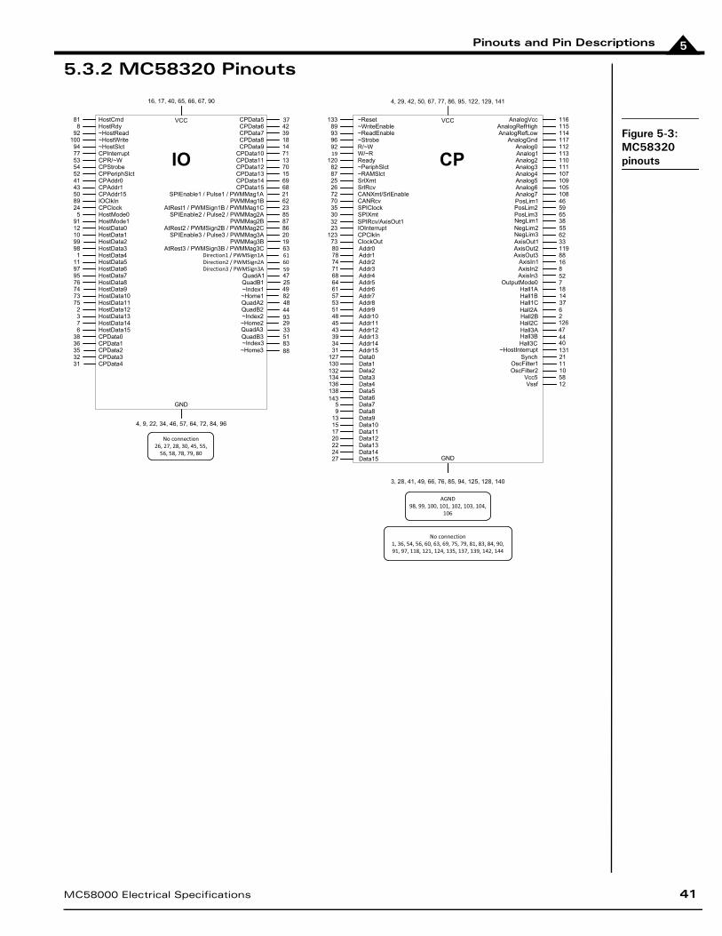
5.3.2 MC58320 Pinouts
Figure 5-3: MC58320 pinouts
VCC
16, 17, 40, 65, 66, 67, 90
~ReadEnable
~PeriphSlct
818
92100
94CPData8CPData9
CPData10CPData11CPData12CPData13CPData14CPData15
HostCmdHostRdy~HostRead~HostWrite~HostSlct
121099981
119795767473752376
3836353231
374239
HostData0HostData1HostData2HostData3HostData4HostData5HostData6HostData7HostData8HostData9HostData10HostData11HostData12HostData13HostData14HostData15CPData0CPData1CPData2CPData3CPData4
CPData5CPData6CPData7
181471137015696821
85
20
7753545241435089245
91
SPIEnable1 / Pulse1 / PWMMag1A
SPIEnable2 / Pulse2 / PWMMag2A
SPIEnable3 / Pulse3 / PWMMag3A
CPInterruptCPR/~WCPStrobeCPPeriphSlctCPAddr0CPAddr1CPAddr15
CPClockIOClkIn
HostMode0HostMode1
472549824844932933518388
QuadA1QuadB1~Index1~Home1QuadA2QuadB2~Index2~Home2QuadA3QuadB3~Index3~Home3
127130132134136138143
59
13151720222427
80787471686461575351484543393431
25267270
23123
SrlXmtSrlRcvCANXmt/SrlEnableCANRcv
IOInterruptCPClkIn
Data0Data1Data2Data3Data4Data5Data6Data7Data8Data9Data10Data11Data12Data13Data14Data15
Addr0Addr1Addr2Addr3Addr4Addr5Addr6Addr7Addr8Addr9Addr10Addr11Addr12Addr13Addr14Addr15
92
1208287
133
R/~W
Ready
~RAMSlct
~Reset
19
93
465965385562
PosLim1PosLim2PosLim3NegLim1NegLim2NegLim3
115114117
331198816852
AxisOut1AxisOut2AxisOut3
AxisIn1AxisIn2AxisIn3
AnalogVccAnalogRefHighAnalogRefLow
AnalogGnd
116
Hall1A
Hall2A
Hall3A
Hall1BHall1C
Hall2CHall2B
Hall3CHall3B
6
181437
2126474440
PWMMag1BAtRest1 / PWMSign1B / PWMMag1C
PWMMag2BAtRest2 / PWMSign2B / PWMMag2C
PWMMag3BAtRest3 / PWMSign3B / PWMMag3C
2362
8786
1963
59
61Direction1 / PWMSign1A
Direction3 / PWMSign3ADirection2 / PWMSign2A 60
W/~R
~HostInterrupt 131Synch 21
Vssf 12
OscFilter1 11OscFilter2 10
Vcc5 58
VCC
4, 29, 42, 50, 67, 77, 86, 95, 122, 129, 141
112113110111107109105108
Analog0Analog1Analog2Analog3Analog4Analog5Analog6Analog7
3530
SPIClockSPIXmt
GND
3, 28, 41, 49, 66, 76, 85, 94, 125, 128, 140
No connection1, 36, 54, 56, 60, 63, 69, 75, 79, 81, 83, 84, 90, 91, 97, 118, 121, 124, 135, 137, 139, 142, 144
GND
4, 9, 22, 34, 46, 57, 64, 72, 84, 96
No connection26, 27, 28, 30, 45, 55,
56, 58, 78, 79, 80
AGND98, 99, 100, 101, 102, 103, 104,
106
73 ClockOut
96 ~Strobe
~WriteEnable89
IO CP
32 SPIRcv/AxisOut1
7OutputMode0
MC58000 Electrical Specifications 41
Pinouts and Pin Descriptions5
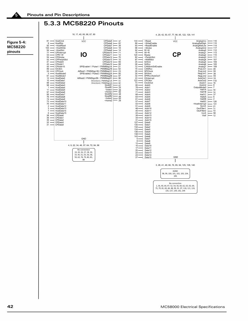
5.3.3 MC58220 Pinouts
Figure 5-4: MC58220 pinouts
VCC
16, 17, 40, 65, 66, 67, 90
~ReadEnable
~PeriphSlct
818
92100
94CPData8CPData9
CPData10CPData11CPData12CPData13CPData14CPData15
HostCmdHostRdy~HostRead~HostWrite~HostSlct
121099981
119795767473752376
3836353231
374239
HostData0HostData1HostData2HostData3HostData4HostData5HostData6HostData7HostData8HostData9HostData10HostData11HostData12HostData13HostData14HostData15CPData0CPData1CPData2CPData3CPData4
CPData5CPData6CPData7
181471137015696821
85
7753545241435089245
91
SPIEnable1 / Pulse1 / PWMMag1A
SPIEnable2 / Pulse2 / PWMMag2A
CPInterruptCPR/~WCPStrobeCPPeriphSlctCPAddr0CPAddr1CPAddr15
CPClockIOClkIn
HostMode0HostMode1
4725498248449329
QuadA1QuadB1~Index1~Home1QuadA2QuadB2~Index2~Home2
127130132134136138143
59
13151720222427
80787471686461575351484543393431
25267270
23123
SrlXmtSrlRcvCANXmt/SrlEnableCANRcv
IOInterruptCPClkIn
Data0Data1Data2Data3Data4Data5Data6Data7Data8Data9Data10Data11Data12Data13Data14Data15
Addr0Addr1Addr2Addr3Addr4Addr5Addr6Addr7Addr8Addr9Addr10Addr11Addr12Addr13Addr14Addr15
92
1208287
133
R/~W
Ready
~RAMSlct
~Reset
19
93
46593855
PosLim1PosLim2NegLim1NegLim2
115114117
33119168
AxisOut1AxisOut2
AxisIn1AxisIn2
AnalogVccAnalogRefHighAnalogRefLow
AnalogGnd
116
Hall1A
Hall2A
Hall1BHall1C
Hall2CHall2B
6
181437
2126
PWMMag1BAtRest1 / PWMSign1B / PWMMag1C
PWMMag2BAtRest2 / PWMSign2B / PWMMag2C
2362
878661Direction1 / PWMSign1A
Direction2 / PWMSign2A 60
W/~R
~HostInterrupt 131Synch 21
Vssf 12
OscFilter1 11OscFilter2 10
Vcc5 58
VCC
4, 29, 42, 50, 67, 77, 86, 95, 122, 129, 141
112113110111107109105108
Analog0Analog1Analog2Analog3Analog4Analog5Analog6Analog7
3530
SPIClockSPIXmt
GND
3, 28, 41, 49, 66, 76, 85, 94, 125, 128, 140
No connection1, 36, 40, 44, 47, 52, 54, 56, 60, 62, 63, 65, 69,
75, 79, 81, 83, 84, 88, 90, 91, 97, 118, 121, 124, 135, 137, 139, 142, 144
GND
4, 9, 22, 34, 46, 57, 64, 72, 84, 96
No connection19, 20, 26, 27, 28, 30, 33, 45, 51, 55, 56, 58, 59, 63, 78, 79, 80, 83,
88
AGND98, 99, 100, 101, 102, 103, 104,
106
73 ClockOut
96 ~Strobe
~WriteEnable89
IO CP
32 SPIRcv/AxisOut1
7OutputMode0
42 MC58000 Electrical Specifications
Pinouts and Pin Descriptions 5
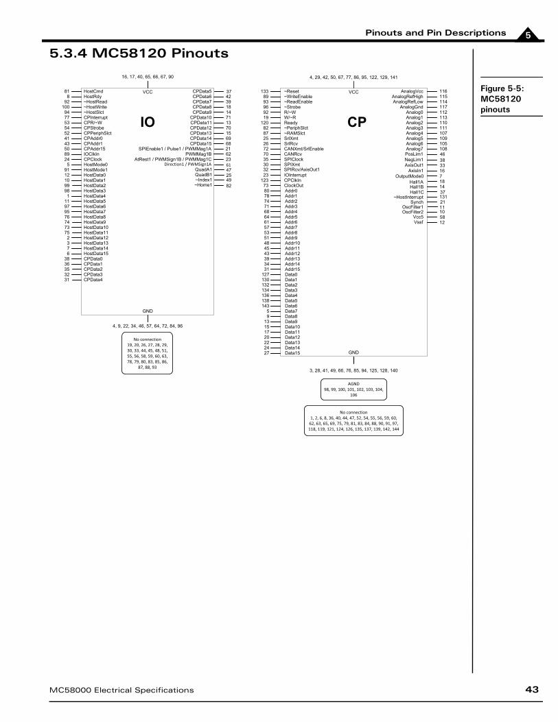
5.3.4 MC58120 Pinouts
Figure 5-5: MC58120 pinouts
VCC
16, 17, 40, 65, 66, 67, 90
~ReadEnable
~PeriphSlct
818
92100
94CPData8CPData9
CPData10CPData11CPData12CPData13CPData14CPData15
HostCmdHostRdy~HostRead~HostWrite~HostSlct
121099981
119795767473752376
3836353231
374239
HostData0HostData1HostData2HostData3HostData4HostData5HostData6HostData7HostData8HostData9HostData10HostData11HostData12HostData13HostData14HostData15CPData0CPData1CPData2CPData3CPData4
CPData5CPData6CPData7
181471137015696821
7753545241435089245
91
SPIEnable1 / Pulse1 / PWMMag1A
CPInterruptCPR/~WCPStrobeCPPeriphSlctCPAddr0CPAddr1CPAddr15
CPClockIOClkIn
HostMode0HostMode1 47
254982
QuadA1QuadB1~Index1~Home1
127130132134136138143
59
13151720222427
80787471686461575351484543393431
25267270
23123
SrlXmtSrlRcvCANXmt/SrlEnableCANRcv
IOInterruptCPClkIn
Data0Data1Data2Data3Data4Data5Data6Data7Data8Data9Data10Data11Data12Data13Data14Data15
Addr0Addr1Addr2Addr3Addr4Addr5Addr6Addr7Addr8Addr9Addr10Addr11Addr12Addr13Addr14Addr15
92
1208287
133
R/~W
Ready
~RAMSlct
~Reset
19
93
4638
PosLim1NegLim1
115114117
3316
AxisOut1AxisIn1
AnalogVccAnalogRefHighAnalogRefLow
AnalogGnd
116
Hall1AHall1BHall1C
181437
PWMMag1BAtRest1 / PWMSign1B / PWMMag1C 23
62
61Direction1 / PWMSign1A
W/~R
~HostInterrupt 131Synch 21
Vssf 12
OscFilter1 11OscFilter2 10
Vcc5 58
VCC
4, 29, 42, 50, 67, 77, 86, 95, 122, 129, 141
112113110111107109105108
Analog0Analog1Analog2Analog3Analog4Analog5Analog6Analog7
3530
SPIClockSPIXmt
GND
3, 28, 41, 49, 66, 76, 85, 94, 125, 128, 140
No connection1, 2, 6, 8, 36, 40, 44, 47, 52, 54, 55, 56, 59, 60,
62, 63, 65, 69, 75, 79, 81, 83, 84, 88, 90, 91, 97, 118, 119, 121, 124, 126, 135, 137, 139, 142, 144
GND
4, 9, 22, 34, 46, 57, 64, 72, 84, 96
No connection19, 20, 26, 27, 28, 29, 30, 33, 44, 45, 48, 51, 55, 56, 58, 59, 60, 63, 78, 79, 80, 83, 85, 86,
87, 88, 93
AGND98, 99, 100, 101, 102, 103, 104,
106
73 ClockOut
96 ~Strobe
~WriteEnable89
IO CP
32 SPIRcv/AxisOut17OutputMode0
MC58000 Electrical Specifications 43
Pinouts and Pin Descriptions5
5.4 MC58x20 Pin Descriptions
5.4.1 I/O Chip
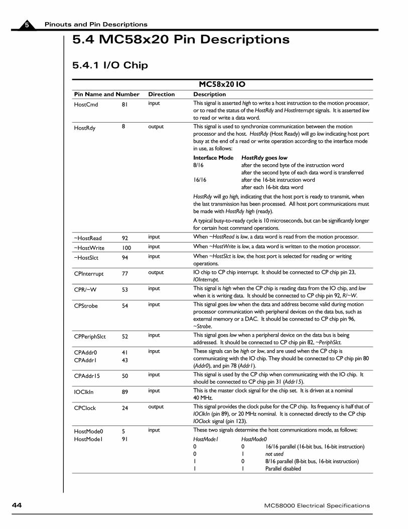
MC58x20 IOPin Name and Number Direction Description
HostCmd 81 input This signal is asserted high to write a host instruction to the motion processor, or to read the status of the HostRdy and HostInterrupt signals. It is asserted low to read or write a data word.
HostRdy 8 output This signal is used to synchronize communication between the motion processor and the host. HostRdy (Host Ready) will go low indicating host port busy at the end of a read or write operation according to the interface mode in use, as follows:
Interface Mode HostRdy goes low8/16 after the second byte of the instruction word
after the second byte of each data word is transferred16/16 after the 16-bit instruction word
after each 16-bit data word
HostRdy will go high, indicating that the host port is ready to transmit, when the last transmission has been processed. All host port communications must be made with HostRdy high (ready).
A typical busy-to-ready cycle is 10 microseconds, but can be significantly longer for certain host command operations.
~HostRead 92 input When ~HostRead is low, a data word is read from the motion processor.
~HostWrite 100 input When ~HostWrite is low, a data word is written to the motion processor.
~HostSlct 94 input When ~HostSlct is low, the host port is selected for reading or writing operations.
CPInterrupt 77 output IO chip to CP chip interrupt. It should be connected to CP chip pin 23, IOInterrupt.
CPR/~W 53 input This signal is high when the CP chip is reading data from the IO chip, and low when it is writing data. It should be connected to CP chip pin 92, R/~W.
CPStrobe 54 input This signal goes low when the data and address become valid during motion processor communication with peripheral devices on the data bus, such as external memory or a DAC. It should be connected to CP chip pin 96, ~Strobe.
CPPeriphSlct 52 input This signal goes low when a peripheral device on the data bus is being addressed. It should be connected to CP chip pin 82, ~PeriphSlct.
CPAddr0CPAddr1
4143
input These signals can be high or low, and are used when the CP chip is communicating with the IO chip. They should be connected to CP chip pin 80 (Addr0), and pin 78 (Addr1).
CPAddr15 50 input This signal is used by the CP chip when communicating with the IO chip. It should be connected to CP chip pin 31 (Addr15).
IOClkIn 89 input This is the master clock signal for the chip set. It is driven at a nominal 40 MHz.
CPClock 24 output This signal provides the clock pulse for the CP chip. Its frequency is half that of IOClkIn (pin 89), or 20 MHz nominal. It is connected directly to the CP chip IOClock signal (pin 123).
HostMode0HostMode1
591
input These two signals determine the host communications mode, as follows:
HostMode1 HostMode00 0 16/16 parallel (16-bit bus, 16-bit instruction)0 1 not used1 0 8/16 parallel (8-bit bus, 16-bit instruction)1 1 Parallel disabled
44 MC58000 Electrical Specifications
Pinouts and Pin Descriptions 5
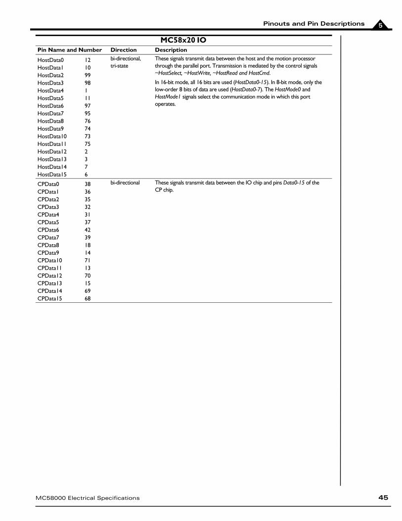
HostData0HostData1HostData2HostData3HostData4HostData5HostData6HostData7HostData8HostData9HostData10HostData11HostData12HostData13HostData14HostData15
121099981119795767473752376
bi-directional,tri-state
These signals transmit data between the host and the motion processor through the parallel port. Transmission is mediated by the control signals ~HostSelect, ~HostWrite, ~HostRead and HostCmd.
In 16-bit mode, all 16 bits are used (HostData0-15). In 8-bit mode, only the low-order 8 bits of data are used (HostData0-7). The HostMode0 and HostMode1 signals select the communication mode in which this port operates.
CPData0CPData1CPData2CPData3CPData4CPData5CPData6CPData7CPData8CPData9CPData10CPData11CPData12CPData13CPData14CPData15
38363532313742391814711370156968
bi-directional These signals transmit data between the IO chip and pins Data0-15 of the CP chip.
MC58x20 IOPin Name and Number Direction Description
MC58000 Electrical Specifications 45
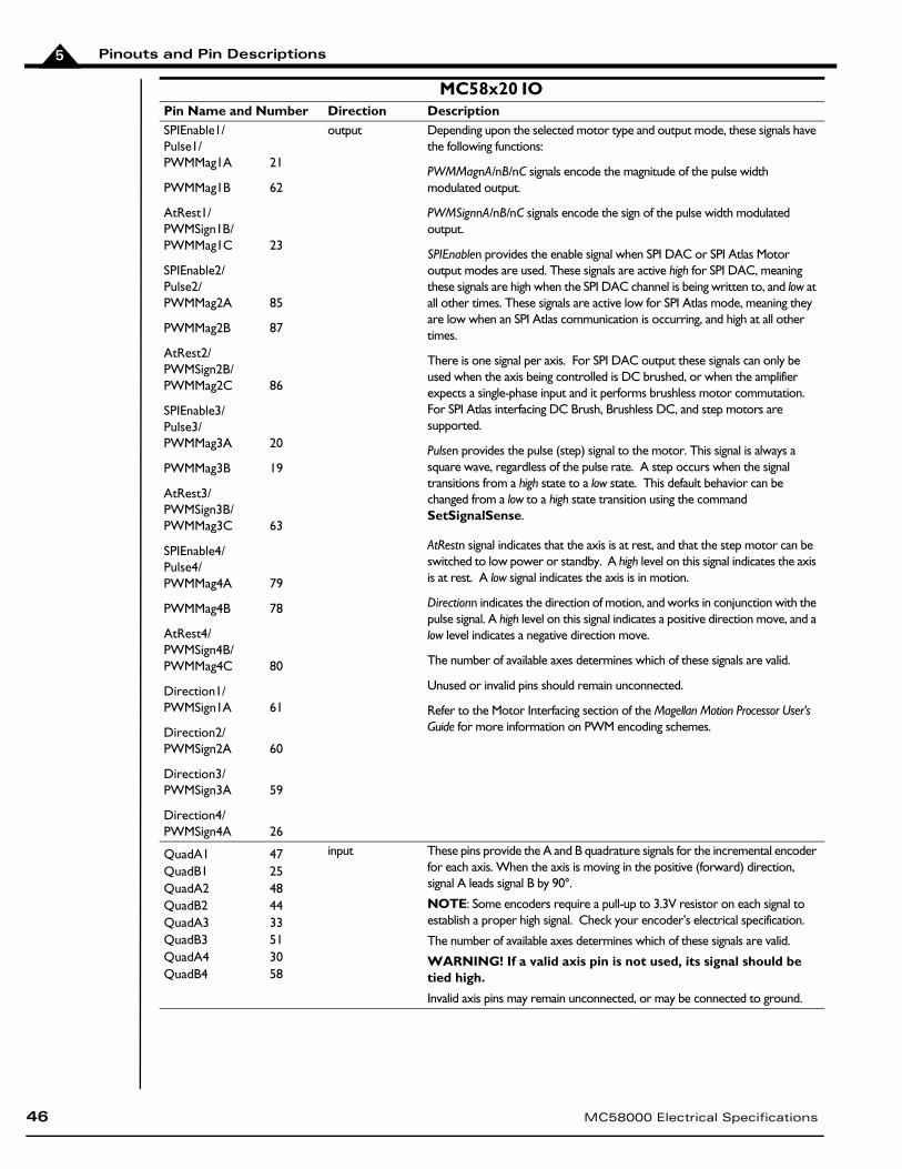
Pinouts and Pin Descriptions5
46 MC58000 Electrical Specifications
SPIEnable1/Pulse1/PWMMag1A
PWMMag1B
AtRest1/PWMSign1B/PWMMag1C
SPIEnable2/Pulse2/PWMMag2A
PWMMag2B
AtRest2/PWMSign2B/PWMMag2C
SPIEnable3/Pulse3/PWMMag3A
PWMMag3B
AtRest3/PWMSign3B/PWMMag3C
SPIEnable4/Pulse4/PWMMag4A
PWMMag4B
AtRest4/PWMSign4B/PWMMag4C
Direction1/PWMSign1A
Direction2/PWMSign2A
Direction3/PWMSign3A
Direction4/PWMSign4A
21
62
23
85
87
86
20
19
63
79
78
80
61
60
59
26
output Depending upon the selected motor type and output mode, these signals have the following functions:
PWMMagnA/nB/nC signals encode the magnitude of the pulse width modulated output.
PWMSignnA/nB/nC signals encode the sign of the pulse width modulated output.
SPIEnablen provides the enable signal when SPI DAC or SPI Atlas Motor output modes are used. These signals are active high for SPI DAC, meaning these signals are high when the SPI DAC channel is being written to, and low at all other times. These signals are active low for SPI Atlas mode, meaning they are low when an SPI Atlas communication is occurring, and high at all other times.
There is one signal per axis. For SPI DAC output these signals can only be used when the axis being controlled is DC brushed, or when the amplifier expects a single-phase input and it performs brushless motor commutation. For SPI Atlas interfacing DC Brush, Brushless DC, and step motors are supported.
Pulsen provides the pulse (step) signal to the motor. This signal is always a square wave, regardless of the pulse rate. A step occurs when the signal transitions from a high state to a low state. This default behavior can be changed from a low to a high state transition using the command SetSignalSense.
AtRestn signal indicates that the axis is at rest, and that the step motor can be switched to low power or standby. A high level on this signal indicates the axis is at rest. A low signal indicates the axis is in motion.
Directionn indicates the direction of motion, and works in conjunction with the pulse signal. A high level on this signal indicates a positive direction move, and a low level indicates a negative direction move.
The number of available axes determines which of these signals are valid.
Unused or invalid pins should remain unconnected.
Refer to the Motor Interfacing section of the Magellan Motion Processor User’s Guide for more information on PWM encoding schemes.
QuadA1QuadB1QuadA2QuadB2QuadA3QuadB3QuadA4QuadB4
4725484433513058
input These pins provide the A and B quadrature signals for the incremental encoder for each axis. When the axis is moving in the positive (forward) direction, signal A leads signal B by 90°.
NOTE: Some encoders require a pull-up to 3.3V resistor on each signal to establish a proper high signal. Check your encoder’s electrical specification.
The number of available axes determines which of these signals are valid.
WARNING! If a valid axis pin is not used, its signal should be tied high.
Invalid axis pins may remain unconnected, or may be connected to ground.
MC58x20 IOPin Name and Number Direction Description

Pinouts and Pin Descriptions 5
~Index1~Index2~Index3~Index4
49938328
input These pins provide the Index quadrature signals for the incremental encoders. A valid index pulse is recognized by the chipset when ~Index, A, and B are all low.
The number of available axes determines which of these signals are valid.
WARNING! If a valid axis pin is not used, its signal should be tied high.
Invalid axis pins may remain unconnected, or may be connected to ground.
~Home1~Home2~Home3~Home4
82298845
input These pins provide the home signals, which are the general-purpose inputs to the position-capture mechanism. A valid home signal is recognized by the chipset when ~Homen goes low. These signals are similar to ~Index, but are not gated by the A and B encoder channels.
The number of available axes determines which of these signals are valid.
WARNING! If a valid axis pin is not used, its signal should be tied high.
Invalid axis pins may remain unconnected, or may be connected to ground.
Vcc 16, 17, 40, 65, 66, 67, 90 All of these pins must be connected to the IO chip digital supply voltage, which should be in the range of 3.0V to 3.6V.
GND 4, 9, 22, 34, 46, 57, 64, 72, 84, 96
IO chip ground. All of these pins must be connected to the digital power supply return.
Not connected 27, 55, 56 These pins must remain unconnected (floating).
MC58x20 IOPin Name and Number Direction Description
MC58000 Electrical Specifications 47
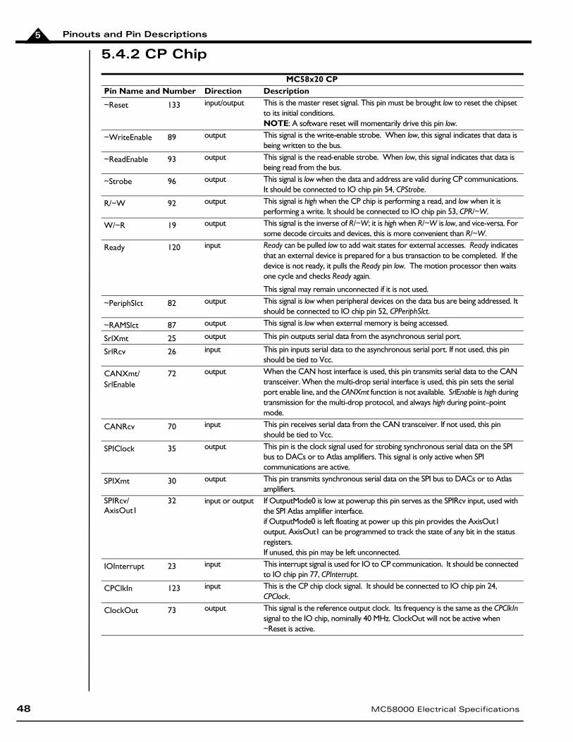
Pinouts and Pin Descriptions5
48 MC58000 Electrical Specifications
5.4.2 CP Chip
MC58x20 CPPin Name and Number Direction Description
~Reset 133 input/output This is the master reset signal. This pin must be brought low to reset the chipset to its initial conditions.NOTE: A software reset will momentarily drive this pin low.
~WriteEnable 89 output This signal is the write-enable strobe. When low, this signal indicates that data is being written to the bus.
~ReadEnable 93 output This signal is the read-enable strobe. When low, this signal indicates that data is being read from the bus.
~Strobe 96 output This signal is low when the data and address are valid during CP communications. It should be connected to IO chip pin 54, CPStrobe.
R/~W 92 output This signal is high when the CP chip is performing a read, and low when it is performing a write. It should be connected to IO chip pin 53, CPR/~W.
W/~R 19 output This signal is the inverse of R/~W; it is high when R/~W is low, and vice-versa. For some decode circuits and devices, this is more convenient than R/~W.
Ready 120 input Ready can be pulled low to add wait states for external accesses. Ready indicates that an external device is prepared for a bus transaction to be completed. If the device is not ready, it pulls the Ready pin low. The motion processor then waits one cycle and checks Ready again.
This signal may remain unconnected if it is not used.
~PeriphSlct 82 output This signal is low when peripheral devices on the data bus are being addressed. It should be connected to IO chip pin 52, CPPeriphSlct.
~RAMSlct 87 output This signal is low when external memory is being accessed.
SrlXmt 25 output This pin outputs serial data from the asynchronous serial port.
SrlRcv 26 input This pin inputs serial data to the asynchronous serial port. If not used, this pin should be tied to Vcc.
CANXmt/SrlEnable
72 output When the CAN host interface is used, this pin transmits serial data to the CAN transceiver. When the multi-drop serial interface is used, this pin sets the serial port enable line, and the CANXmt function is not available. SrlEnable is high during transmission for the multi-drop protocol, and always high during point–point mode.
CANRcv 70 input This pin receives serial data from the CAN transceiver. If not used, this pin should be tied to Vcc.
SPIClock 35 output This pin is the clock signal used for strobing synchronous serial data on the SPI bus to DACs or to Atlas amplifiers. This signal is only active when SPI communications are active.
SPIXmt 30 output This pin transmits synchronous serial data on the SPI bus to DACs or to Atlas amplifiers.
SPIRcv/AxisOut1
32 input or output If OutputMode0 is low at powerup this pin serves as the SPIRcv input, used with the SPI Atlas amplifier interface.if OutputMode0 is left floating at power up this pin provides the AxisOut1 output. AxisOut1 can be programmed to track the state of any bit in the status registers.If unused, this pin may be left unconnected.
IOInterrupt 23 input This interrupt signal is used for IO to CP communication. It should be connected to IO chip pin 77, CPInterrupt.
CPClkIn 123 input This is the CP chip clock signal. It should be connected to IO chip pin 24, CPClock.
ClockOut 73 output This signal is the reference output clock. Its frequency is the same as the CPClkIn signal to the IO chip, nominally 40 MHz. ClockOut will not be active when ~Reset is active.
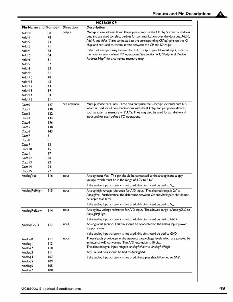
Pinouts and Pin Descriptions 5
Addr0Addr1Addr2Addr3Addr4Addr5Addr6Addr7Addr8Addr9Addr10Addr11Addr12Addr13Addr14Addr15
80787471686461575351484543393431
output Multi-purpose address lines. These pins comprise the CP chip’s external address bus, and are used to select devices for communication over the data bus. Addr0, Addr1, and Addr15 are connected to the corresponding CPAddr pins on the IO chip, and are used to communicate between the CP and IO chips.
Other address pins may be used for DAC output, parallel word input, external memory, or user-defined I/O operations. See Section 6.3, “Peripheral Device Address Map,” for a complete memory map.
Data0Data1Data2Data3Data4Data5Data6Data7Data8Data9Data10Data11Data12Data13Data14Data15
1271301321341361381435913151720222427
bi-directional Multi-purpose data lines. These pins comprise the CP chip’s external data bus, which is used for all communications with the IO chip and peripheral devices such as external memory or DACs. They may also be used for parallel-word input and for user-defined I/O operations.
AnalogVcc 116 input Analog input Vcc. This pin should be connected to the analog input supply voltage, which must be in the range of 3.0V to 3.6V.
If the analog input circuitry is not used, this pin should be tied to Vcc.
AnalogRefHigh 115 input Analog high voltage reference for A/D input. The allowed range is 2V to AnalogVcc. Furthermore, the difference between Vcc and AnalogVcc should not be larger than 0.3V.
If the analog input circuitry is not used, this pin should be tied to Vcc.
AnalogRefLow 114 input Analog low voltage reference for A/D input. The allowed range is AnalogGND to AnalogRefHigh.
If the analog input circuitry is not used, this pin should be tied to GND.
AnalogGND 117 input Analog input ground. This pin should be connected to the analog input power supply return.
If the analog input circuitry is not used, this pin should be tied to GND.
Analog0Analog1Analog2Analog3Analog4Analog5Analog6Analog7
112113110111107109105108
input These signals provide general-purpose analog voltage levels which are sampled by an internal A/D converter. The A/D resolution is 10 bits.The allowed signal input range is AnalogRefLow to AnalogRefHigh.
Any unused pins should be tied to AnalogGND.
If the analog input circuitry is not used, these pins should be tied to GND.
MC58x20 CPPin Name and Number Direction Description
MC58000 Electrical Specifications 49
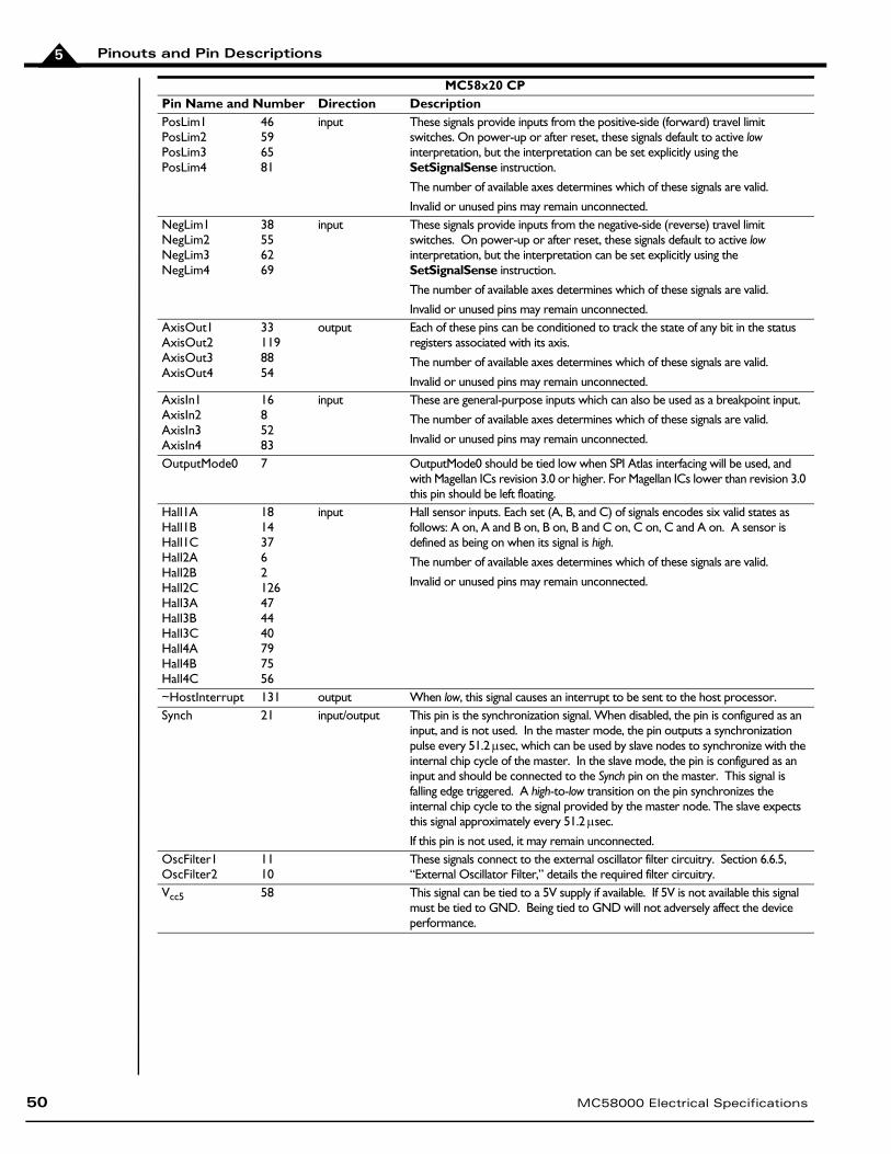
Pinouts and Pin Descriptions5
PosLim1PosLim2PosLim3PosLim4
46596581
input These signals provide inputs from the positive-side (forward) travel limit switches. On power-up or after reset, these signals default to active low interpretation, but the interpretation can be set explicitly using the SetSignalSense instruction.
The number of available axes determines which of these signals are valid.
Invalid or unused pins may remain unconnected.NegLim1NegLim2NegLim3NegLim4
38556269
input These signals provide inputs from the negative-side (reverse) travel limit switches. On power-up or after reset, these signals default to active low interpretation, but the interpretation can be set explicitly using the SetSignalSense instruction.
The number of available axes determines which of these signals are valid.
Invalid or unused pins may remain unconnected.AxisOut1AxisOut2AxisOut3AxisOut4
331198854
output Each of these pins can be conditioned to track the state of any bit in the status registers associated with its axis.
The number of available axes determines which of these signals are valid.
Invalid or unused pins may remain unconnected.AxisIn1AxisIn2AxisIn3AxisIn4
1685283
input These are general-purpose inputs which can also be used as a breakpoint input.
The number of available axes determines which of these signals are valid.
Invalid or unused pins may remain unconnected.
OutputMode0 7 OutputMode0 should be tied low when SPI Atlas interfacing will be used, and with Magellan ICs revision 3.0 or higher. For Magellan ICs lower than revision 3.0 this pin should be left floating.
Hall1AHall1BHall1CHall2AHall2BHall2CHall3AHall3BHall3CHall4AHall4BHall4C
18143762126474440797556
input Hall sensor inputs. Each set (A, B, and C) of signals encodes six valid states as follows: A on, A and B on, B on, B and C on, C on, C and A on. A sensor is defined as being on when its signal is high.
The number of available axes determines which of these signals are valid.
Invalid or unused pins may remain unconnected.
~HostInterrupt 131 output When low, this signal causes an interrupt to be sent to the host processor.Synch 21 input/output This pin is the synchronization signal. When disabled, the pin is configured as an
input, and is not used. In the master mode, the pin outputs a synchronization pulse every 51.2sec, which can be used by slave nodes to synchronize with the internal chip cycle of the master. In the slave mode, the pin is configured as an input and should be connected to the Synch pin on the master. This signal is falling edge triggered. A high-to-low transition on the pin synchronizes the internal chip cycle to the signal provided by the master node. The slave expects this signal approximately every 51.2sec.
If this pin is not used, it may remain unconnected.OscFilter1OscFilter2
1110
These signals connect to the external oscillator filter circuitry. Section 6.6.5, “External Oscillator Filter,” details the required filter circuitry.
Vcc5 58 This signal can be tied to a 5V supply if available. If 5V is not available this signal must be tied to GND. Being tied to GND will not adversely affect the device performance.
MC58x20 CPPin Name and Number Direction Description
50 MC58000 Electrical Specifications

Pinouts and Pin Descriptions 5
MC58000 Electrical Specifications 51
Vssf 12 This signal must be tied to Vcc. It must also be tied to pin 28 via a bypass capacitor. A ceramic capacitor with a value between 0.1 F and 0.01F should be used.
Vcc 4, 29, 42, 50, 67, 77, 86, 95, 122, 129, 141
CP digital supply voltage. All of these pins must be connected to the supply voltage. Vcc must be in the range of 3.0V to 3.6V.
GND 3, 28, 41, 49, 66, 76, 85, 94, 125, 128, 140
CP digital supply ground. All of these pins must be connected to the digital power supply return.
AGND 98, 99, 100, 101, 102, 103, 104, 106
These signals must be tied to AnalogGND.
If the analog input circuitry is not used, these pins must be tied to GND.No connection 1, 7, 36, 60, 63, 84, 90, 91,
97, 118, 121, 124, 135, 137, 139, 142, 144
These signals must remain unconnected.
MC58x20 CPPin Name and Number Direction Description
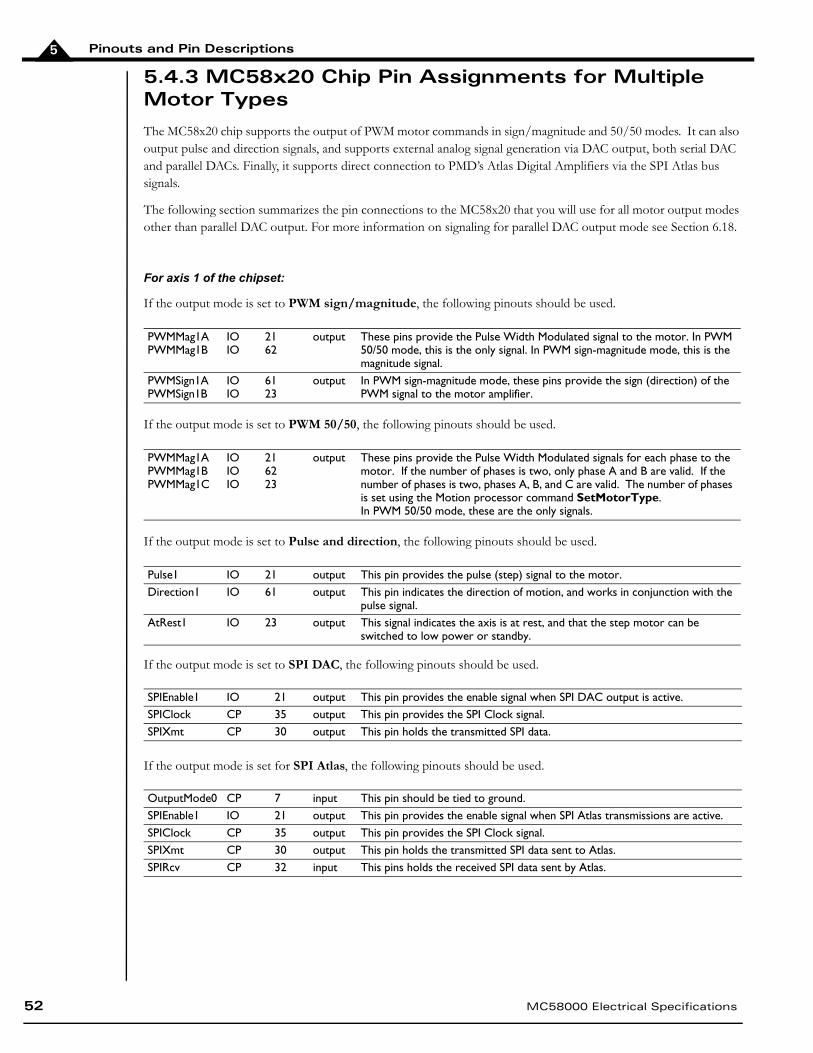
Pinouts and Pin Descriptions5
5.4.3 MC58x20 Chip Pin Assignments for Multiple Motor Types
The MC58x20 chip supports the output of PWM motor commands in sign/magnitude and 50/50 modes. It can also output pulse and direction signals, and supports external analog signal generation via DAC output, both serial DAC and parallel DACs. Finally, it supports direct connection to PMD’s Atlas Digital Amplifiers via the SPI Atlas bus signals.
The following section summarizes the pin connections to the MC58x20 that you will use for all motor output modes other than parallel DAC output. For more information on signaling for parallel DAC output mode see Section 6.18.
For axis 1 of the chipset:
If the output mode is set to PWM sign/magnitude, the following pinouts should be used.
If the output mode is set to PWM 50/50, the following pinouts should be used.
If the output mode is set to Pulse and direction, the following pinouts should be used.
If the output mode is set to SPI DAC, the following pinouts should be used.
If the output mode is set for SPI Atlas, the following pinouts should be used.
PWMMag1APWMMag1B
IOIO
2162
output These pins provide the Pulse Width Modulated signal to the motor. In PWM 50/50 mode, this is the only signal. In PWM sign-magnitude mode, this is the magnitude signal.
PWMSign1APWMSign1B
IOIO
6123
output In PWM sign-magnitude mode, these pins provide the sign (direction) of the PWM signal to the motor amplifier.
PWMMag1APWMMag1BPWMMag1C
IOIOIO
216223
output These pins provide the Pulse Width Modulated signals for each phase to the motor. If the number of phases is two, only phase A and B are valid. If the number of phases is two, phases A, B, and C are valid. The number of phases is set using the Motion processor command SetMotorType.In PWM 50/50 mode, these are the only signals.
Pulse1 IO 21 output This pin provides the pulse (step) signal to the motor.Direction1 IO 61 output This pin indicates the direction of motion, and works in conjunction with the
pulse signal.AtRest1 IO 23 output This signal indicates the axis is at rest, and that the step motor can be
switched to low power or standby.
SPIEnable1 IO 21 output This pin provides the enable signal when SPI DAC output is active.SPIClock CP 35 output This pin provides the SPI Clock signal.SPIXmt CP 30 output This pin holds the transmitted SPI data.
OutputMode0 CP 7 input This pin should be tied to ground.SPIEnable1 IO 21 output This pin provides the enable signal when SPI Atlas transmissions are active.SPIClock CP 35 output This pin provides the SPI Clock signal.SPIXmt CP 30 output This pin holds the transmitted SPI data sent to Atlas.SPIRcv CP 32 input This pins holds the received SPI data sent by Atlas.
52 MC58000 Electrical Specifications
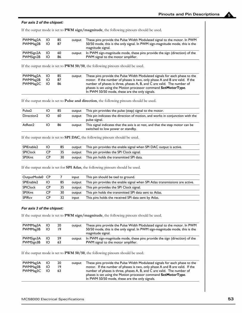
Pinouts and Pin Descriptions 5
For axis 2 of the chipset:
If the output mode is set to PWM sign/magnitude, the following pinouts should be used.
If the output mode is set to PWM 50/50, the following pinouts should be used.
If the output mode is set to Pulse and direction, the following pinouts should be used.
If the output mode is set to SPI DAC, the following pinouts should be used.
If the output mode is set for SPI Atlas, the following pinouts should be used.
For axis 3 of the chipset:
If the output mode is set to PWM sign/magnitude, the following pinouts should be used.
If the output mode is set to PWM 50/50, the following pinouts should be used.
PWMMag2APWMMag2B
IOIO
8587
output These pins provide the Pulse Width Modulated signal to the motor. In PWM 50/50 mode, this is the only signal. In PWM sign-magnitude mode, this is the magnitude signal.
PWMSign2APWMSign2B
IOIO
6086
output In PWM sign-magnitude mode, these pins provide the sign (direction) of the PWM signal to the motor amplifier.
PWMMag2APWMMag2BPWMMag2C
IOIOIO
858786
output These pins provide the Pulse Width Modulated signals for each phase to the motor. If the number of phases is two, only phase A and B are valid. If the number of phases is three, phases A, B, and C are valid. The number of phases is set using the Motion processor command SetMotorType.In PWM 50/50 mode, these are the only signals.
Pulse2 IO 85 output This pin provides the pulse (step) signal to the motor.Direction2 IO 60 output This pin indicates the direction of motion, and works in conjunction with the
pulse signal.AtRest2 IO 86 output This signal indicates that the axis is at rest, and that the step motor can be
switched to low power or standby.
SPIEnable2 IO 85 output This pin provides the enable signal when SPI DAC output is active.SPIClock CP 35 output This pin provides the SPI Clock signal.SPIXmt CP 30 output This pin holds the transmitted SPI data.
OutputMode0 CP 7 input This pin should be tied to ground.SPIEnable2 IO 85 output This pin provides the enable signal when SPI Atlas transmissions are active.SPIClock CP 35 output This pin provides the SPI Clock signal.SPIXmt CP 30 output This pin holds the transmitted SPI data sent to Atlas.SPIRcv CP 32 input This pins holds the received SPI data sent by Atlas.
PWMMag3APWMMag3B
IOIO
2019
output These pins provide the Pulse Width Modulated signal to the motor. In PWM 50/50 mode, this is the only signal. In PWM sign-magnitude mode, this is the magnitude signal.
PWMSign3APWMSign3B
IOIO
5963
output In PWM sign-magnitude mode, these pins provide the sign (direction) of the PWM signal to the motor amplifier.
PWMMag3APWMMag3BPWMMag3C
IOIOIO
201963
output These pins provide the Pulse Width Modulated signals for each phase to the motor. If the number of phases is two, only phase A and B are valid. If the number of phases is three, phases A, B, and C are valid. The number of phases is set using the Motion processor command SetMotorType.In PWM 50/50 mode, these are the only signals.
MC58000 Electrical Specifications 53
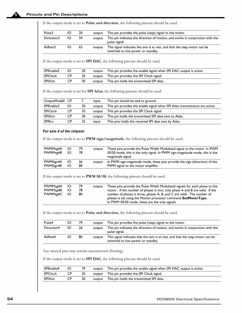
Pinouts and Pin Descriptions5
If the output mode is set to Pulse and direction, the following pinouts should be used.
If the output mode is set to SPI DAC, the following pinouts should be used.
If the output mode is set for SPI Atlas, the following pinouts should be used.
For axis 4 of the chipset:
If the output mode is set to PWM sign/magnitude, the following pinouts should be used.
If the output mode is set to PWM 50/50, the following pinouts should be used.
If the output mode is set to Pulse and direction, the following pinouts should be used.
Any unused pins may remain unconnected (floating).
If the output mode is set to SPI DAC, the following pinouts should be used.
Pulse3 IO 20 output This pin provides the pulse (step) signal to the motor.Direction3 IO 59 output This pin indicates the direction of motion, and works in conjunction with the
pulse signal.AtRest3 IO 63 output This signal indicates the axis is at rest, and that the step motor can be
switched to low power or standby.
SPIEnable3 IO 20 output This pin provides the enable signal when SPI DAC output is active.SPIClock CP 35 output This pin provides the SPI Clock signal.SPIXmt CP 30 output This pin holds the transmitted SPI data.
OutputMode0 CP 7 input This pin should be tied to ground.SPIEnable3 IO 20 output This pin provides the enable signal when SPI Atlas transmissions are active.SPIClock CP 35 output This pin provides the SPI Clock signal.SPIXmt CP 30 output This pin holds the transmitted SPI data sent to Atlas.SPIRcv CP 32 input This pins holds the received SPI data sent by Atlas.
PWMMag4APWMMag4B
IOIO
7978
output These pins provide the Pulse Width Modulated signal to the motor. In PWM 50/50 mode, this is the only signal. In PWM sign-magnitude mode, this is the magnitude signal.
PWMSign4APWMSign4B
IOIO
2680
output In PWM sign-magnitude mode, these pins provide the sign (direction) of the PWM signal to the motor amplifier.
PWMMag4APWMMag4BPWMMag4C
IOIOIO
797880
output These pins provide the Pulse Width Modulated signals for each phase to the motor. If the number of phases is two, only phase A and B are valid. If the number of phases is three, phases A, B, and C are valid. The number of phases is set using the Motion processor command SetMotorType.In PWM 50/50 mode, these are the only signals.
Pulse4 IO 79 output This pin provides the pulse (step) signal to the motor.Direction4 IO 26 output This pin indicates the direction of motion, and works in conjunction with the
pulse signal.AtRest4 IO 80 output This signal indicates that the axis is at rest, and that the step motor can be
switched to low power or standby.
SPIEnable4 IO 79 output This pin provides the enable signal when SPI DAC output is active.SPIClock CP 35 output This pin provides the SPI Clock signal.SPIXmt CP 30 output This pin holds the transmitted SPI data.
54 MC58000 Electrical Specifications
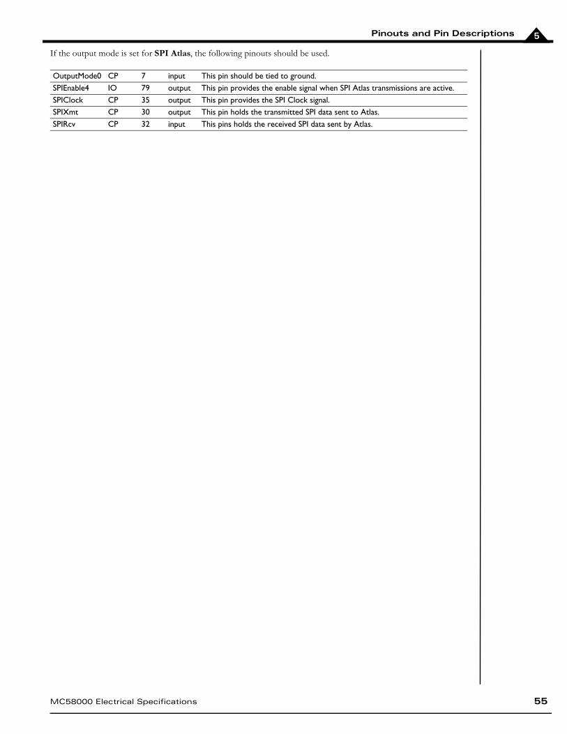
Pinouts and Pin Descriptions 5
If the output mode is set for SPI Atlas, the following pinouts should be used.
OutputMode0 CP 7 input This pin should be tied to ground.SPIEnable4 IO 79 output This pin provides the enable signal when SPI Atlas transmissions are active.SPIClock CP 35 output This pin provides the SPI Clock signal.SPIXmt CP 30 output This pin holds the transmitted SPI data sent to Atlas.SPIRcv CP 32 input This pins holds the received SPI data sent by Atlas.
MC58000 Electrical Specifications 55
Prodigy-PCI Motion Card User’s Guide 565656
6
6. Application Notes — MC58110 and MC58x20In This ChapterGeneral Design NotesDesign TipsPeripheral Device Address MappingDevice InitializationPower SuppliesClock Generator, Grounding and Decoupling, and Device ResetSerial Communication Interface (SCI)CAN Communication InterfaceExternal MemoryAsynchronous SRAM Dual Port Synchronous SRAM (DPRAM)Using the On-chip ADCUser I/O SpaceParallel Word Position InputParallel Communication InterfaceOvercurrent and Emergency Braking Circuits for Motor DriversDC Brush Motor Control Using SPI Interfaced DACsBrushless DC Motor Control Using High-Precision Parallel DACsSingle-Axis Magellan with Brushless DC AtlasMulti-Axis Magellan with DC Brush & Step Motor AtlasPulse & Direction Mode Output Connected to AtlasUsing PWM for DC Brush, Brushless DC and Microstepping MotorsUsing the Allegro A3977 to Drive Microstepping Motors
6.1 General Design NotesLogic functions presented in the example schematics are implemented by standard logic gates. In cases where specific parameters are of significance (propagation delay, voltage levels, etc…) a recommended part number is given.
One important point of note is that the single and dual chip configurations of Magellan share several signals with the same name that reside on physically different chips. For example, on the MC58x20 the PWM signals are located on the IO chip while on the MC58110 the PWM signals are located on the CP chip. As such, care should be taken to ensure that during the initial schematic layout that the correct CP chip is selected.
In the schematics, pins with multiple functions are referenced by the name corresponding to the specified functionality. For example, pin 54 on the MC58110 CP is named “Direction1 / SPIEnable1 / PWMSign1A” but will be referenced by the name
“SPIEnable1” in the SPI DAC example and “PWMSign1A” in the DC brush motor schematics.
The schematic designs presented in this chapter are accurate to the best of PMD’s knowledge. They are intended for reference only and have not all been tested in hardware implementations.
Application Notes — MC58110 and MC58x206
57 MC58000 Electrical Specifications
6.1.1 Interfacing to Other Logic FamiliesWhen integrating different logic families, consideration should be given to timing, logic level compatibility, and output drive capabilities. The Magellan CP and IO chips are 3.3V CMOS input/output compatible and cannot be directly interfaced to 5V CMOS components. In order to drive a 5V CMOS device, level shifters from the 5V CMOS AHCT (or the slower HCT) families can be used. When using a 5V CMOS component to drive the CP, a voltage divider may be used or a member from the CMOS 3.3V LVT family may serve as a level shifter.
6.2 Design TipsThe following are recommendations/requirements for the design of circuits which utilize a PMD Motion Processor.
6.2.1 Serial InterfaceThe serial interface is a convenient interface which can be used before host software has been written to communicate through the parallel interface. It is recommended that even if the serial interface is not utilized as a standard communication interface, that the serial receive and transmit signals are brought to test points so that they may be connected during initial board configuration/debugging. This is especially important during the prototype phase. The serial receive line should include a pull-up resistor to avoid spurious interrupts when it is not connected to a transceiver.
If the serial configuration decode logic is not implemented, and the serial interface is used for debugging as previously mentioned, the CP data bus should be tied high. This places the serial interface in a default configuration of 57,600, n, 8, 1 after power on or reset.
6.2.2 Controlling PWM Output During ResetWhen the motion processor is in a reset state (when the reset line is held low), or immediately after a power on, the PWM outputs can be in an unknown state, causing undesirable motor movement. It is recommended that the enable line of any motor amplifier be held in a disabled state by the host processor or some logic circuitry until communi-cation to the motion processor is established. This can be in the form of a delay circuit on the amplifier enable line after power up, or the enable line can be ANDed with the CP reset line.
6.2.3 Using a Non-standard System Clock FrequencyIt is often desirable to share a common clock among several components in a design. In the case of the PMD Motion Processors, it is possible to use a clock below the standard value of 40 MHz. In this case, all system frequencies will be reduced as a fraction of the input clock versus the standard 40 MHz clock. The following list details the affected system parameters.
Serial baud rate
PWM carrier frequency
Cycle time
Commutation rate
For example, if an input clock of 34 MHz is used with a serial baud rate of 9600, the following timing changes will result.
Serial baud rate decreases to 9600 bps *34/40 = 8160 bps
PWM frequency decreases to 20 kHz *34/40 = 17 kHz
Total cycle time increases by a factor of 40/34
The commutation rate for brushless axes decreases to 10 kHz *34/40 = 8.5 kHz

Application Notes — MC58110 and MC58x20 6
MC58000 Electrical Specifications 58
6.3 Peripheral Device Address MapDevice addresses on the CP chip’s external bus are memory-mapped to the following locations.
6.4 Device InitializationFollowing a hardware or software reset, the motion processor reads from three external configuration registers to determine the desired settings for the motor type, serial communication, and CAN communication. These reads take place sequentially using the peripheral address read. The timing for this read is shown in Figure 4-14.
6.4.1 Motor Type ConfigurationWhen the motor type configuration is read, the 16-bit word is interpreted according to the following table.
Address Device Description0100h Motor type configuration Contains the configuration data for the per axis motor type selection0200h Serial port configuration Contains the configuration data (transmission rate, parity, stop bits,
etc.) for the asynchronous serial port0400h CAN port configuration Contains the configuration data (baud rate and node ID) for the CAN
controller0800h Parallel-word encoder Base address for parallel-word feedback devices1000h User-defined Base address for user-defined I/O devices2000h RAM page pointer Page pointer to external memory4000h Motor-output DACs Base address for motor-output D/A converters8000h reserved
Bit Number Name Instance Encoding0-2 axis1 DC Brushless (3 phase)
DC Brushless (2 phase)Microstepper (3 phase)Microstepper (2 phase)StepperreservedDC Brushed
012345-67
3 reserved Zero 04-6 axis2 DC Brushless (3 phase)
DC Brushless (2 phase)Microstepper (3 phase)Microstepper (2 phase)StepperreservedDC Brushed
012345-67
7 reserved Zero 08-10 axis3 DC Brushless (3 phase)
DC Brushless (2 phase)Microstepper (3 phase)Microstepper (2 phase)StepperreservedDC Brushed
012345-67
11 reserved Zero 012-14 axis4 DC Brushless (3 phase)
DC Brushless (2 phase)Microstepper (3 phase)Microstepper (2 phase)StepperreservedDC Brushed
012345-67
15 reserved Zero 0

Application Notes — MC58110 and MC58x206
6.4.2 Serial Port Configuration
When the serial configuration is read, the 16-bit word is interpreted according to the following table.
6.4.3 CAN Port Configuration
When the CAN configuration is read, the 16-bit word is interpreted according to the following table.
As an alternative to decoding each configuration address, a special condition occurs when the device powers up and the external bus is pulled high. In this case, the device will read the contents of each configuration register as containing the value 0xffff. When this occurs, the device will configure the serial port as 57,600, n, 8, 1; the CAN port as 20,000 bps with a NodeID of zero; and the motor type will be set to DC Brushed for all available axes.
Bit Number Name Instance Encoding
0-3 transmission rate 1200 baud2400960019200 57600 115200 230400 460800
01234567
4-5 parity noneoddeven
012
6 stop bits 12
01
7-8 protocol Point-to-pointMulti-drop using idle-line detectionreservedreserved
0123
11-15 multi-drop address Address 0Address 1…Address 31
01…31
Bit Number Name Instance Encoding0-6 nodeID Address 0
Address 1…Address 127
01…127
7-12 reserved reserved reserved13-15 transmission rate 1,000,000 baud
800,000500,000250,000125,000 50,000 20,000 10,000
01234567
59 MC58000 Electrical Specifications
Application Notes — MC58110 and MC58x20
MC58000 Electrical Specifications 60
6
If the serial or CAN port is not required, the circuitry for decoding the relevant addresses can be omitted, and the CANRcv and SrlRcv signals can remain disconnected to prevent the chip from responding to either of these communication inputs.
Since CANbus cannot be used when serial multi-drop mode is selected, if using CANbus the serial port configu-ration register, described in section 6.4.2, must have bits 7 and 8 tied low (selecting point to point serial commu-nications).

Application Notes — MC58110 and MC58x206
6.5 Power SuppliesIn the schematic shown in Figure 6-1, the design is powered by an external 5V DC power source. The MC58000 device requires a 3.3V supply and an optional 5V input. The 5V input to the motion processor can be omitted if 5V is not required elsewhere in the design. The 3.3V digital supply, VCC, is generated by an LT1086-3.3, a 1.5Amp fixed 3.3V low-dropout voltage regulator. Components with a larger power capacity are also available, such as the LT1085-3.3.
If the CP’s analog-to-digital converter (ADC) is used, it should be supplied with a filtered 3.3V supply. The +3.3Vs supply is a filtered version of the VCC supply, which is used to supply the ADC and its related conditioning circuitry. The extra filtering is used to provide additional decoupling of the analog elements from the digital elements in the circuitry.
The following is the list of supplies which are referenced in the example schematics:
+5Vs: a filtered version of 5VCC. This is used for analog components requiring +5V supplies. The extra filtering is used to reduce the voltage ripple, and to generate additional decoupling of the analog elements from the digital elements in the circuitry.
±15Vs: ±15V supplies, used for analog components dealing with large input or output voltage swings; usu-ally when interfacing to motors or sensors. The Calex 5D15.033 is a 1W ±15V DC/DC converter which delivers ±33 mA. Depending on the current load of the final design, a larger power capacity DC/DC con-verter may be required. An LC filter is used to reduce the voltage ripple.
±10Vref: two high-precision ±10V reference voltages for driving precise motor commands when using high-precision DACs. The AD688 offers 12-bit absolute accuracy, which may be increased by additional trimming circuitry. The AD688 also offers low noise and a low temperature coefficient, and as such is well suited for the high-precision DAC example.
Notes:
The schematic in Figure 6-1 should be used for reference only. The actual supplies used should be designed according to the stability and precision requirements of the application. The power supplies presented here are only designed to meet the requirements of the example schematics.
Power supplies for the motor drivers are not shown. Care should be taken when designing these power supplies, as they should be capable of sinking high switching currents.
61 MC58000 Electrical Specifications
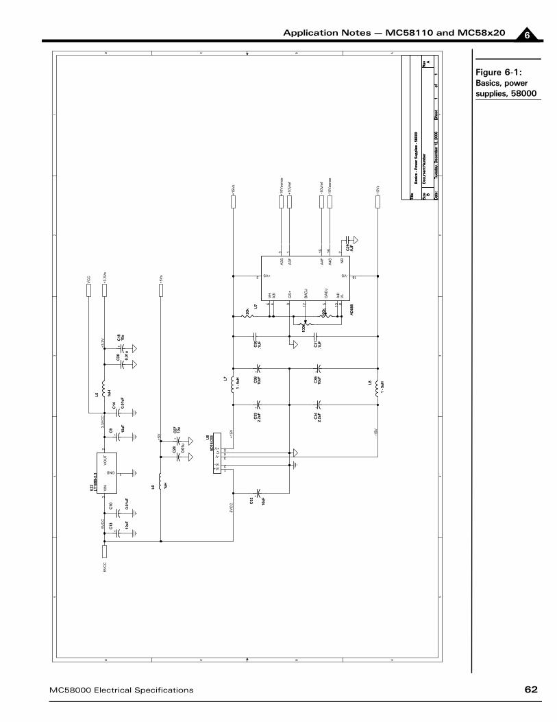
Application Notes — MC58110 and MC58x20 6
Figure 6-1:Basics, power supplies, 58000
5 5
4 4
3 3
2 2
1 1
DD
CC
BB
AA
3.3V
CC
5VC
C
+5V -1
5V
+15V
5VC
C
+3.3
V5V
CC
+15V
s
+3.3
Vs
-15V
s
+10V
ref
-10V
ref
VC
C
+5V
s
+10V
sens
e
-10V
sens
e
Title
Siz
eD
ocum
ent N
umbe
rR
ev
Dat
e:S
heet
of
A
Bas
ics
- Pow
er S
uppl
ies
- 580
00
B
11
Tues
day,
Dec
embe
r 12,
200
6
Title
Siz
eD
ocum
ent N
umbe
rR
ev
Dat
e:S
heet
of
A
Bas
ics
- Pow
er S
uppl
ies
- 580
00
B
11
Tues
day,
Dec
embe
r 12,
200
6
Title
Siz
eD
ocum
ent N
umbe
rR
ev
Dat
e:S
heet
of
A
Bas
ics
- Pow
er S
uppl
ies
- 580
00
B
11
Tues
day,
Dec
embe
r 12,
200
6
U8
5D15
.033U
85D
15.0
33
VI+ 1VI- 2
-V 3C 4+V 5
C14 0.01
uF
C14 0.01
uF
C29
.1U
FC
29.1
UF
U7
AD
688
U7
AD
688
+VS2 -VS 16
A3S
3
A3F
1
A4F
15
A4S
14
VH
6A
3I4
GS
+9
BA
DJ
12
VL
8A
4I13
GA
DJ
5
NR
7
L7
1 - 5
uHL7
1 - 5
uH
+C
32
10uF
+C
32
10uF
C30
.1U
FC
30.1
UF
L8
1 - 5
uHL8
1 - 5
uH
100k
100k
L5 1uH
L5 1uH
L6 1uH
L6 1uH
100k
100k
C20 0.01
u
C20 0.01
u
+C
1810
u+
C18
10u
+C
2710
u+
C27
10u
20k
20k
+C
3610
uF+
C36
10uF
+C
13
10uF
+C
13
10uF
+C
3510
uF+
C35
10uF
C28 0.01
u
C28 0.01
u
+C
342.
2uF
+C
342.
2uF
U22
LT10
86-3
.3U
22LT
1086
-3.3
VIN
3
GND 1
VO
UT
2
C10
0.01
uF
C10
0.01
uF
C31
.1U
FC
31.1
UF
+C
9
10uF
+C
9
10uF
+C
332.
2uF
+C
332.
2uF
MC58000 Electrical Specifications 62
Application Notes — MC58110 and MC58x206
6.6 Clock Generator, Grounding and Decoupling, and Device Reset
6.6.1 Clock Generator — MC58110
The nominal clock frequency of the MC58110 CP is 20 MHz. A separate 20 MHz clock may be generated for the device and peripherals or a pre-existing derivative of a clock generated on the board may be used. If an existing clock is to be used, ensure that the input voltages and timing requirements of the MC58110 are met and that the correct frequency is generated.
For any frequency in the range, the bypass capacitor (labeled C3 in Figure 6-2 and Figure 6-3) should be between 0.1 and 0.01 µF, ceramic, and it should have private and as short as possible traces to the pins. This method will reduce noise and jitter, and increase isolation.
6.6.2 Clock Generator — MC58x20
The nominal clock frequency of the MC58x20 IO is 40 MHz. The IO chip generates a nominal 20 MHz clock signal for the CP chip by dividing the input frequency by two. When applying a lower clock frequency to the IO chip, the CP external oscillator filter circuit must adhere to the values listed in Section 6.6.5, “External Oscillator Filter.”
63 MC58000 Electrical Specifications

Application Notes — MC58110 and MC58x20 6
6.6.3 Grounding and Decoupling
Each component should be decoupled with the use of large capacitors, usually tantalum 6.7-10 µF in parallel, with a set of 10-100 nF ceramic capacitors placed as close as possible between each one of the power supply pins and ground. This general rule applies to all analog and digital components, although in some of the schematics that follow these capacitors are not shown for reasons of brevity. In some cases, especially in analog parts, it may be beneficial to run a separate power line from the power supply to the component in order to prevent power supply fluctuations from impacting low-level signal components.
The same points should be considered when designing the ground. The schematics in Figure 6-2 and Figure 6-3 show a star connection at one point in the power supply. Care should be taken to ensure that voltage differences do not accumulate between the grounds, especially in mixed signal components such DACs and ADCs.
Additional isolation, for example ferrite beads, may be inserted between the analog and digital grounds to suppress high frequency ground noise. Some components, such as motor drivers, require special grounding. The system designer should refer to the component data sheets of selected components in order to ensure correct usage of the grounding methods.
6.6.4 Decoupling of the On-chip ADC
The voltage supply to the ADC should be decoupled with the use of a 2.2-6.8 µF tantalum capacitor in parallel with a 0.01-0.1 µF ceramic capacitor placed as close as possible to the power supply and ground pins. For additional isolation purposes, an additional 0.01-0.1 µF ceramic capacitor should be placed across AnalogRefLow and AnalogRefHigh.
MC58000 Electrical Specifications 64

Application Notes — MC58110 and MC58x206
Figure 6-2:Basics, clock and bypass caps, 58110
5 5
4 4
3 3
2 2
1 1
DD
CC
BB
AA
CP
Clk
In
VC
C
Dat
a7
Dat
a2
Dat
a12
Dat
a6
Dat
a15
Dat
a11
Dat
a5
Dat
a9D
ata1
0
Dat
a4
Dat
a14
Dat
a1
Dat
a8
Dat
a3
Dat
a13
Dat
a0
VC
C
VC
C
CP
Clk
In Add
r7
Add
r2
Add
r12
Add
r6
Add
r15
Add
r11
Add
r5
Add
r9A
ddr1
0
Add
r4
Add
r14
Add
r1
Add
r8
Add
r3
Add
r13
Add
r0
GN
DO
SC
F2O
SC
F1
GN
D
AG
ND
VC
C
Dat
a[0.
.15]
Clo
ckO
ut
W/~
RR
/~W
~Stro
be~R
eadE
nabl
e~W
riteE
nabl
e
~Per
iphS
lct
~RA
MS
lct
SrlX
mt
Can
Xm
t / S
rlEna
ble
SP
IClo
ckS
PIX
mt
~Res
et
Rea
dy
SrlR
cv
CA
NR
cv
+3.3
Vs
Pul
se1
/ PW
MM
ag1A
Dire
ctio
n1 /
SP
IEna
ble1
/ P
WM
Sig
n1A
PW
MM
ag1B
PW
MS
ign1
BP
WM
Mag
1CP
WM
Sig
n1C
Ana
log0
Ana
log1
Ana
log2
VC
C
Add
r[0..1
5]
Syn
ch
Title
Siz
eD
ocum
ent N
umbe
rR
ev
Dat
e:S
heet
of
A
Bas
ics
- Clo
ck a
nd B
ypas
s C
aps
- 581
10
B
11
Tues
day,
Dec
embe
r 12,
200
6
Title
Siz
eD
ocum
ent N
umbe
rR
ev
Dat
e:S
heet
of
A
Bas
ics
- Clo
ck a
nd B
ypas
s C
aps
- 581
10
B
11
Tues
day,
Dec
embe
r 12,
200
6
Title
Siz
eD
ocum
ent N
umbe
rR
ev
Dat
e:S
heet
of
A
Bas
ics
- Clo
ck a
nd B
ypas
s C
aps
- 581
10
B
11
Tues
day,
Dec
embe
r 12,
200
6
20M
Hz
Clk
Gen
erat
or
Note:
All digital inputs have internal
pull ups and may be left floating
The capacitor array with C=0.1uF
should be placed as close as possible to each of
the VCC pins of the CP chip
See capacitor array comment
Note:
All unused analog inputs
should be tied to AGND
+Ta
ntal
um6.
8uF
+Ta
ntal
um6.
8uF
U13
MC
5811
0 - C
P
U13
MC
5811
0 - C
P
~Res
et13
3~W
riteE
nabl
e89
~Stro
be96
R/~
W92
W/~
R19
Rea
dy12
0~P
erip
hSlc
t82
~RA
MS
lct
87S
rlXm
t25
SrlR
cv26
CA
NX
mt/S
rlEna
ble
72C
AN
Rcv
70
IOIn
terr
upt
23C
PC
lkIn
123
Clo
ckO
ut73
Add
r080
Add
r178
Add
r274
Add
r371
Add
r468
Add
r564
Add
r661
Add
r757
Add
r853
Add
r951
Add
r10
48A
ddr1
145
Add
r12
43A
ddr1
339
Add
r14
34A
ddr1
531
Dat
a012
7D
ata1
130
Dat
a213
2D
ata3
134
Dat
a413
6D
ata5
138
Dat
a614
3D
ata7
5D
ata8
9D
ata9
13D
ata1
015
Dat
a11
17D
ata1
220
Dat
a13
22D
ata1
424
Dat
a15
27
GND 3GND 28GND 41GND 49GND 66GND 76GND 85GND 94GND 125GND 128GND 140
AGND 98AGND 99AGND 100AGND 101AGND 102AGND 103AGND 104AGND 106
VCC4VCC29VCC42VCC50VCC67VCC77VCC86VCC95VCC122VCC129VCC141
Ana
logV
cc11
6A
nalo
gRef
Hig
h11
5
Ana
logR
efLo
w11
4A
nalo
gGnd
117
Ana
log0
112
Ana
log1
113
Ana
log2
110
Ana
log3
111
Ana
log4
107
Ana
log5
109
Ana
log6
105
Ana
log7
108
Pos
Lim
146
Qua
dAux
B1
81
Neg
Lim
138
~Ind
ex1
69
Axi
sOut
132
Qua
dAux
A1
88
Axi
sIn1
16
Par
alle
lEna
ble
8Q
uadA
183
Qua
dB1
79
~Hom
e175
~Hos
tInte
rrup
t13
1
Syn
ch21
Osc
Filte
r111
Osc
Filte
r210
Vcc
558
Vss
f12
~Rea
dEna
ble
93
SP
IClo
ck35
SP
IXm
t30
Hal
l1A
18H
all1
B14
Hal
l1C
37
Pul
se1
/ PW
MM
ag1A
56D
irect
ion1
/ S
PIE
nabl
e1 /
PW
MS
ign1
A54
AtR
ese1
/ P
WM
Mag
1B52
PW
MS
ign1
B47
PW
MM
ag1C
44P
WM
Sig
n1C
40
0.1u
F0.
1uF
CC
C37
.01u
FC
37.0
1uF
CC+
C40
10uF
+C
4010
uFCC
+C
3810
uF+
C38
10uF
CCCC
CC
0.1u
F0.
1uF
CCCC
R1
24R1
24
CC
C3
.047
uFC
3.0
47uF
U23
CTX
309F
BU
23C
TX30
9FB
OE
1
GND 2
OU
T3
VDD4
CC
C1
.15u
FC
1.1
5uF
R7 10
kR
7 10k
Opt
iona
lO
ptio
nal
C2
.003
3uF
C2
.003
3uF
CC
65 MC58000 Electrical Specifications
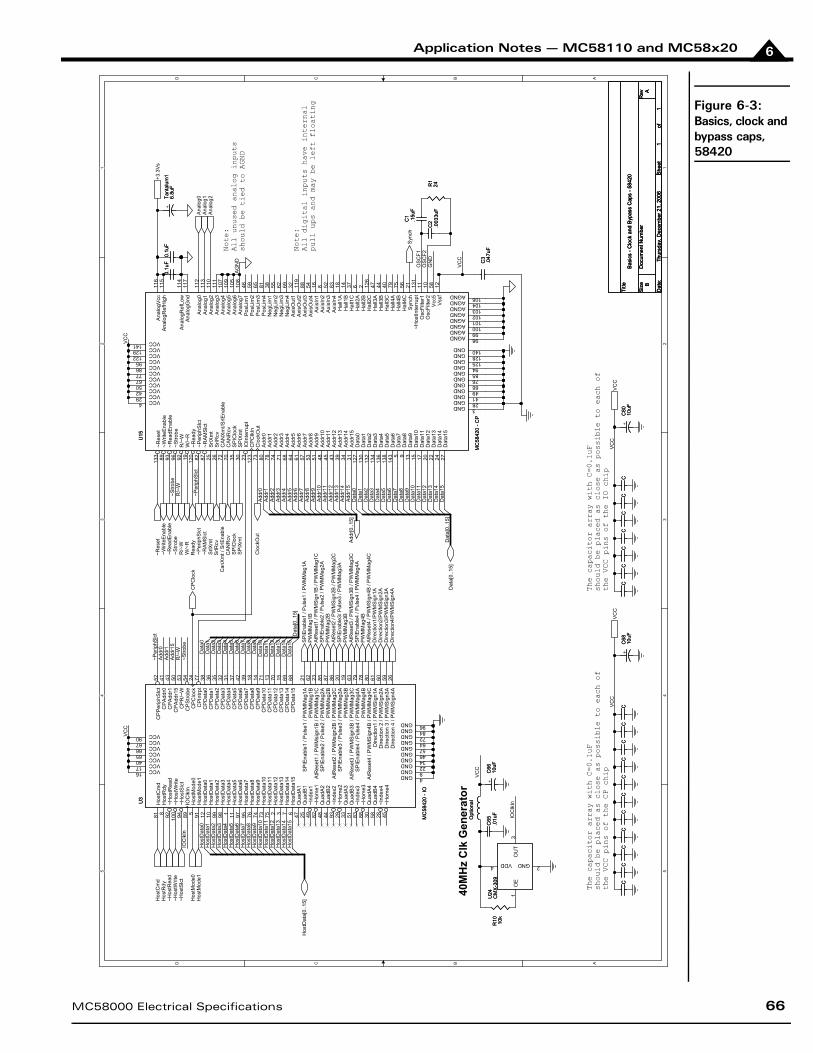
Application Notes — MC58110 and MC58x20 6
Figure 6-3:Basics, clock and bypass caps, 58420
5 5
4 4
3 3
2 2
1 1
DD
CC
BB
AA
~Stro
beR
/~W
~Per
iphS
lct
Dat
a7
Dat
a2
Dat
a12
Dat
a6
Dat
a15
Dat
a11
Dat
a5
Dat
a9D
ata1
0
Dat
a4
Dat
a14
Dat
a1
Dat
a8
Dat
a3
Dat
a13
Dat
a0
Dat
a[0.
.15]
Add
r7
Add
r2
Add
r12
Add
r6
Add
r15
Add
r11
Add
r5
Add
r9A
ddr1
0
Add
r4
Add
r14
Add
r1
Add
r8
Add
r3
Add
r13
Add
r0
Dat
a7
Dat
a2
Dat
a12
Dat
a6
Dat
a15
Dat
a11
Dat
a5
Dat
a9D
ata1
0
Dat
a4
Dat
a14
Dat
a8
Dat
a3
Dat
a1
Dat
a13
Dat
a0
Dat
a[0.
.15]
~Per
iphS
lct
~Stro
beR
/~W
Add
r15
Add
r1A
ddr0
AG
ND
VC
C
GN
DO
SC
F2O
SC
F1
Hos
tDat
a7
Hos
tDat
a2
Hos
tDat
a12
Hos
tDat
a6
Hos
tDat
a15
Hos
tDat
a11
Hos
tDat
a5
Hos
tDat
a9H
ostD
ata1
0
Hos
tDat
a4
Hos
tDat
a14
Hos
tDat
a8
Hos
tDat
a3
Hos
tDat
a1
Hos
tDat
a13
Hos
tDat
a0
VC
CV
CC
IOC
lkIn
IOC
lkIn
VC
C
VC
CV
CC
W/~
RR
/~W
~Stro
be~R
eadE
nabl
e~W
riteE
nabl
e
~Per
iphS
lct
~RA
MS
lct
SrlX
mt
Can
Xm
t / S
rlEna
ble
SP
IClo
ckS
PIX
mt
~Res
et
Rea
dy
SrlR
cv
CA
NR
cv
Dat
a[0.
.15]
Clo
ckO
ut
+3.3
Vs
Ana
log0
Ana
log1
Ana
log2
SP
IEna
ble1
/ P
ulse
1 / P
WM
Mag
1AP
WM
Mag
1BA
tRes
et1
/ PW
MS
ign1
B /
PW
MM
ag1C
SP
IEna
ble2
/ P
ulse
2 / P
WM
Mag
2AP
WM
Mag
2BA
tRes
et2
/ PW
MS
ign2
B /
PW
MM
ag2C
SP
IEna
ble3
/ Pul
se3
/ PW
MM
ag3A
PW
MM
ag3B
AtR
eset
3 / P
WM
Sig
n3B
/ P
WM
Mag
3CS
PIE
nabl
e4 /
Pul
se4
/ PW
MM
ag4A
PW
MM
ag4B
AtR
eset
4 / P
WM
Sig
n4B
/ P
WM
Mag
4CD
irect
ion1
/PW
MS
ign1
AD
irect
ion2
/PW
MS
ign2
AD
irect
ion3
/PW
MS
ign3
AD
irect
ion4
/PW
MS
ign4
ACP
Clo
ck
Hos
tCm
dH
ostR
dy~H
ostR
ead
~Hos
tWrit
e~H
ostS
lct
Hos
tMod
e0H
ostM
ode1
Hos
tDat
a[0.
.15]
VC
CV
CC
Add
r[0..1
5]
Syn
ch
Title
Siz
eD
ocum
ent N
umbe
rR
ev
Dat
e:S
heet
of
A
Bas
ics
- Clo
ck a
nd B
ypas
s C
aps
- 584
20
B
11
Thur
sday
, Dec
embe
r 21,
200
6
Title
Siz
eD
ocum
ent N
umbe
rR
ev
Dat
e:S
heet
of
A
Bas
ics
- Clo
ck a
nd B
ypas
s C
aps
- 584
20
B
11
Thur
sday
, Dec
embe
r 21,
200
6
Title
Siz
eD
ocum
ent N
umbe
rR
ev
Dat
e:S
heet
of
A
Bas
ics
- Clo
ck a
nd B
ypas
s C
aps
- 584
20
B
11
Thur
sday
, Dec
embe
r 21,
200
6
40M
Hz
Clk
Gen
erat
or
The capacitor array with C=0.1uF
should be placed as close as possible to each of
the VCC pins of the CP chip
The capacitor array with C=0.1uF
should be placed as close as possible to each of
the VCC pins of the IO chip
Note:
All digital inputs have internal
pull ups and may be left floating
Note:
All unused analog inputs
should be tied to AGND
CCCC
CC
R1
24R1
24
Opt
iona
lO
ptio
nal
CCCC
U15
MC
5842
0 - C
P
U15
MC
5842
0 - C
P
~Res
et13
3~W
riteE
nabl
e89
~Stro
be96
R/~
W92
W/~
R19
~Rea
dy12
0~P
erip
hSlc
t82
~RA
MS
lct
87S
rlXm
t25
SrlR
cv26
CA
NX
mt/S
rlEna
ble
72C
AN
Rcv
70S
PIC
lock
35S
PIX
mt
30IO
Inte
rrup
t23
CP
Clk
In12
3C
lock
Out
73A
ddr0
80A
ddr1
78A
ddr2
74A
ddr3
71A
ddr4
68A
ddr5
64A
ddr6
61A
ddr7
57A
ddr8
53A
ddr9
51A
ddr1
048
Add
r11
45A
ddr1
243
Add
r13
39A
ddr1
434
Add
r15
31D
ata0
127
Dat
a113
0D
ata2
132
Dat
a313
4D
ata4
136
Dat
a513
8D
ata6
143
Dat
a75
Dat
a89
Dat
a913
Dat
a10
15D
ata1
117
Dat
a12
20D
ata1
322
Dat
a14
24D
ata1
527
GND 3GND 28GND 41GND 49GND 66GND 76GND 85GND 94GND 125GND 128GND 140
AGND 98AGND 99AGND 100AGND 101AGND 102AGND 103AGND 104AGND 106
VCC4VCC29VCC42VCC50VCC67VCC77VCC86VCC95VCC122VCC129VCC141
Ana
logV
cc11
6A
nalo
gRef
Hig
h11
5
Ana
logR
efLo
w11
4A
nalo
gGnd
117
Ana
log0
112
Ana
log1
113
Ana
log2
110
Ana
log3
111
Ana
log4
107
Ana
log5
109
Ana
log6
105
Ana
log7
108
Pos
Lim
146
Pos
Lim
259
Pos
Lim
365
Pos
Lim
481
Neg
Lim
138
Neg
Lim
255
Neg
Lim
362
Neg
Lim
469
Axi
sOut
132
Axi
sOut
211
9A
xisO
ut3
88A
xisO
ut4
54A
xisI
n116
Axi
sIn2
8A
xisI
n352
Axi
sIn4
83H
all1
A18
Hal
l1B
14H
all1
C37
Hal
l2A
6H
all2
B2
Hal
l2C
126
Hal
l3A
47H
all3
B44
Hal
l3C
40H
all4
A79
Hal
l4B
75H
all4
C56
~Hos
tInte
rrup
t13
1S
ynch
21
Osc
Filte
r111
Osc
Filte
r210
Vcc
558
Vss
f12
~Rea
dEna
ble
93
+C
6810
uF+
C68
10uF
C1
.15u
FC
1.1
5uF
U3
MC
5842
0 - I
O
U3
MC
5842
0 - I
O
Hos
tCm
d81
Hos
tRdy
8~H
ostR
ead
92~H
ostW
rite
100
~Hos
tSlc
t94
CP
Intrp
t77
CP
R/~
W53
CP
Stro
be54
CP
Per
iphS
lct
52C
PA
ddr0
41C
PA
ddr1
43C
PA
ddr1
550
IOC
lkIn
89C
PC
lock
24H
ostM
ode0
5H
ostM
ode1
91H
ostD
ata0
12H
ostD
ata1
10H
ostD
ata2
99H
ostD
ata3
98H
ostD
ata4
1H
ostD
ata5
11H
ostD
ata6
97H
ostD
ata7
95H
ostD
ata8
76H
ostD
ata9
74H
ostD
ata1
073
Hos
tDat
a11
75H
ostD
ata1
22
Hos
tDat
a13
3H
ostD
ata1
47
Hos
tDat
a15
6Q
uadA
147
Qua
dB1
25~I
ndex
149
~Hom
e182
Qua
dA2
48Q
uadB
244
~Ind
ex2
93~H
ome2
29Q
uadA
333
Qua
dB3
51~I
ndex
383
~Hom
e388
CP
Dat
a038
CP
Dat
a136
CP
Dat
a235
CP
Dat
a332
CP
Dat
a431
CP
Dat
a537
CP
Dat
a642
CP
Dat
a739
CP
Dat
a818
CP
Dat
a914
CP
Dat
a10
71C
PD
ata1
113
CP
Dat
a12
70C
PD
ata1
315
CP
Dat
a14
69C
PD
ata1
568
SP
IEna
ble1
/ P
ulse
1 / P
WM
Mag
1A21
PW
MM
ag1B
62A
tRes
et1
/ PW
Msi
gn1B
/ P
WM
Mag
1C23
SP
IEna
ble2
/ P
ulse
2 / P
WM
Mag
2A85
PW
MM
ag2B
87A
tRes
et2
/ PW
Msi
gn2B
/ P
WM
Mag
2C86
SP
IEna
ble3
/ P
ulse
3 / P
WM
Mag
3A20
PW
MM
ag3B
19A
tRes
et3
/ PW
MS
ign3
B /
PW
MM
ag3C
63
Dire
ctio
n1 /
PW
MS
ign1
A61
Dire
ctio
n 2
/ PW
MS
ign2
A60
Dire
ctio
n 3
/ PW
MS
ign3
A59
VCC16VCC17VCC40VCC65VCC66VCC67VCC90
GND 4GND 9GND 22GND 34
GND 57GND 64GND 72GND 84GND 96
GND 46
~Ind
ex4
28~H
ome4
45
Qua
dA4
30Q
uadB
458
Dire
ctio
n 4
/ PW
MS
ign4
A26
SP
IEna
ble4
/ P
ulse
4 / P
WM
Mag
4A79
PW
MM
ag4B
78A
tRes
et4
/ PW
MS
ign4
B /
PW
MM
ag4C
80
CCCC
U24
CM
X-3
09U
24C
MX
-309
OE
1
GND 2
OU
T3
VDD4
CC
C2
.003
3uF
C2
.003
3uF
+C
8010
uF+
C80
10uF
CC
+Ta
ntal
um1
6.8u
F+
Tant
alum
16.
8uF
R10 10
kR
10 10k
C65
.01u
FC
65.0
1uF
CCCC
CCCC
CC
+C
6610
uF+
C66
10uF
CC
C3
.047
uFC
3.0
47uF
0.1u
F0.
1uF
CC
0.1u
F0.
1uF
CCCC
MC58000 Electrical Specifications 66
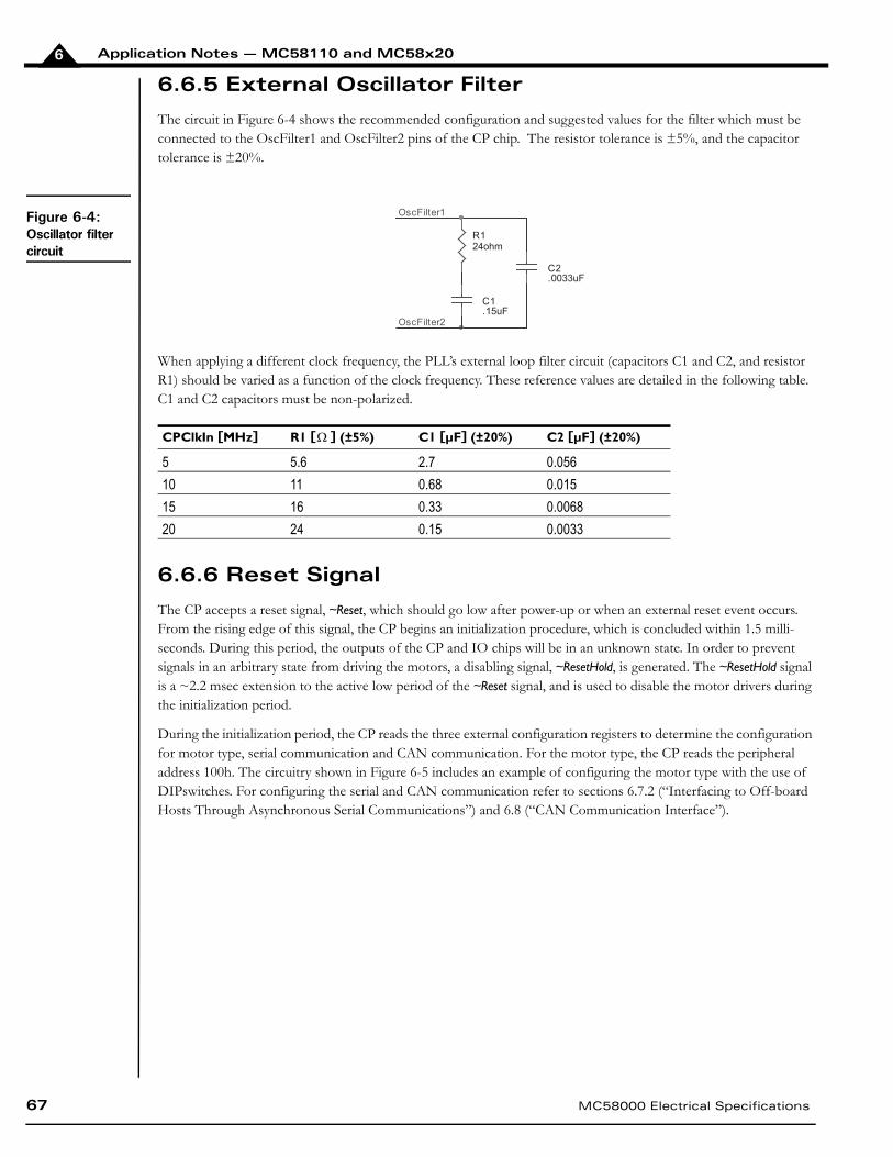
Application Notes — MC58110 and MC58x206
6.6.5 External Oscillator Filter
The circuit in Figure 6-4 shows the recommended configuration and suggested values for the filter which must be connected to the OscFilter1 and OscFilter2 pins of the CP chip. The resistor tolerance is ±5%, and the capacitor tolerance is ±20%.
Figure 6-4:Oscillator filter circuit
When applying a different clock frequency, the PLL’s external loop filter circuit (capacitors C1 and C2, and resistor R1) should be varied as a function of the clock frequency. These reference values are detailed in the following table. C1 and C2 capacitors must be non-polarized.
6.6.6 Reset Signal
The CP accepts a reset signal, ~Reset, which should go low after power-up or when an external reset event occurs. From the rising edge of this signal, the CP begins an initialization procedure, which is concluded within 1.5 milli-seconds. During this period, the outputs of the CP and IO chips will be in an unknown state. In order to prevent signals in an arbitrary state from driving the motors, a disabling signal, ~ResetHold, is generated. The ~ResetHold signal is a ~2.2 msec extension to the active low period of the ~Reset signal, and is used to disable the motor drivers during the initialization period.
During the initialization period, the CP reads the three external configuration registers to determine the configuration for motor type, serial communication and CAN communication. For the motor type, the CP reads the peripheral address 100h. The circuitry shown in Figure 6-5 includes an example of configuring the motor type with the use of DIPswitches. For configuring the serial and CAN communication refer to sections 6.7.2 (“Interfacing to Off-board Hosts Through Asynchronous Serial Communications”) and 6.8 (“CAN Communication Interface”).
CPClkIn [MHz] R1 [ ] (±5%) C1 [µF] (±20%) C2 [µF] (±20%)
5 5.6 2.7 0.056
10 11 0.68 0.015
15 16 0.33 0.0068
20 24 0.15 0.0033
R124ohm
C1.15uF
C2.0033uF
OscFilter1
OscFilter2
67 MC58000 Electrical Specifications
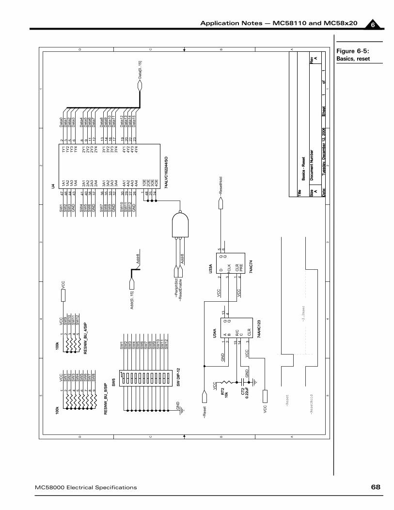
Application Notes — MC58110 and MC58x20 6
Figure 6-5:Basics, reset
5 5
4 4
3 3
2 2
1 1
DD
CC
BB
AA
SW
12
SW
8
SW
1S
W2
SW
3S
W4
SW
5S
W6
SW
7
GN
D
SW
9S
W8
SW
10
SW
1S
W2
SW
3S
W4
SW
7
SW
5S
W6
VC
C
SW
10S
W11
SW
9V
CC
SW
1S
W2
SW
3
SW
5S
W4
SW
6
SW
11
Add
r8
GN
DD
ata7
Dat
a2
Dat
a12
Dat
a6
Dat
a15
Dat
a11
Dat
a5
Dat
a9D
ata1
0
Dat
a4
Dat
a14
Dat
a1
Dat
a8
Dat
a3
Dat
a13
Dat
a0
Add
r8
SW
12
SW
7S
W8
SW
9
SW
10
GN
D
GN
D
GN
D
SW
11S
W12
VC
C
VC
CV
CC
GN
DV
CC
GN
D
VC
C
Dat
a[0.
.15]
Add
r[0..1
5]
~Per
iphS
lct
~Rea
dEna
ble
~Res
etH
old
~Res
et
VC
C
Title
Siz
eD
ocum
ent N
umbe
rR
ev
Dat
e:S
heet
of
A
Bas
ics
- Res
et
A
11
Tues
day,
Dec
embe
r 12,
200
6
Title
Siz
eD
ocum
ent N
umbe
rR
ev
Dat
e:S
heet
of
A
Bas
ics
- Res
et
A
11
Tues
day,
Dec
embe
r 12,
200
6
Title
Siz
eD
ocum
ent N
umbe
rR
ev
Dat
e:S
heet
of
A
Bas
ics
- Res
et
A
11
Tues
day,
Dec
embe
r 12,
200
6
~Reset
~ResetHold
~2.2msec
U34
A
74A
HC
123
U34
A
74A
HC
123
A1
B2
CLR
3
Q13
Q4
C14
R/C
15
U4
74A
LVC
1622
44/S
O
U4
74A
LVC
1622
44/S
O
1Y1
21Y
23
1Y3
51Y
46
2Y1
82Y
29
2Y3
112Y
412
3Y1
133Y
214
3Y3
163Y
417
4Y1
194Y
220
4Y3
224Y
423
1A4
431A
344
1A2
461A
147
2A4
372A
338
2A2
402A
141
3A4
323A
333
3A2
353A
136
4A4
264A
327
4A2
294A
130
1OE
1
4OE
243O
E25
2OE
48
100k
RE
SN
W_B
U_4
/SIP
100k
RE
SN
W_B
U_4
/SIP
1 2 3 4 5
U33
A
74A
C74
U33
A
74A
C74
CLR
1
D2
CLK
3
PR
E4
Q5
Q6
RT2
10kRT2
10k
100k
RE
SN
W_B
U_8
/SIP
100k
RE
SN
W_B
U_8
/SIP
1 2 3 4 5 6 7 8 9
SW
5
SW
DIP
-12
SW
5
SW
DIP
-12
CT2
0.22
uFC
T20.
22uF
MC58000 Electrical Specifications 68
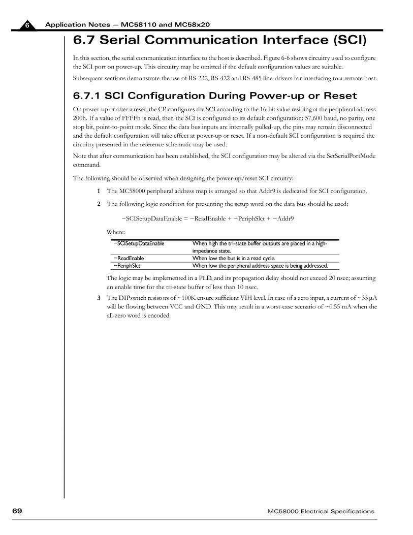
Application Notes — MC58110 and MC58x206
6.7 Serial Communication Interface (SCI)In this section, the serial communication interface to the host is described. Figure 6-6 shows circuitry used to configure the SCI port on power-up. This circuitry may be omitted if the default configuration values are suitable.
Subsequent sections demonstrate the use of RS-232, RS-422 and RS-485 line-drivers for interfacing to a remote host.
6.7.1 SCI Configuration During Power-up or Reset On power-up or after a reset, the CP configures the SCI according to the 16-bit value residing at the peripheral address 200h. If a value of FFFFh is read, then the SCI is configured to its default configuration: 57,600 baud, no parity, one stop bit, point-to-point mode. Since the data bus inputs are internally pulled-up, the pins may remain disconnected and the default configuration will take effect at power-up or reset. If a non-default SCI configuration is required the circuitry presented in the reference schematic may be used.
Note that after communication has been established, the SCI configuration may be altered via the SetSerialPortMode command.
The following should be observed when designing the power-up/reset SCI circuitry:
1 The MC58000 peripheral address map is arranged so that Addr9 is dedicated for SCI configuration.
2 The following logic condition for presenting the setup word on the data bus should be used:
~SCISetupDataEnable = ~ReadEnable + ~PeriphSlct + ~Addr9
Where:
The logic may be implemented in a PLD, and its propagation delay should not exceed 20 nsec; assuming an enable time for the tri-state buffer of less than 10 nsec.
3 The DIPswitch resistors of ~100K ensure sufficient VIH level. In case of a zero input, a current of ~33 µAwill be flowing between VCC and GND. This may result in a worst-case scenario of ~0.55 mA when theall-zero word is encoded.
~SCISetupDataEnable When high the tri-state buffer outputs are placed in a high-impedance state.
~ReadEnable When low the bus is in a read cycle.~PeriphSlct When low the peripheral address space is being addressed.
69 MC58000 Electrical Specifications
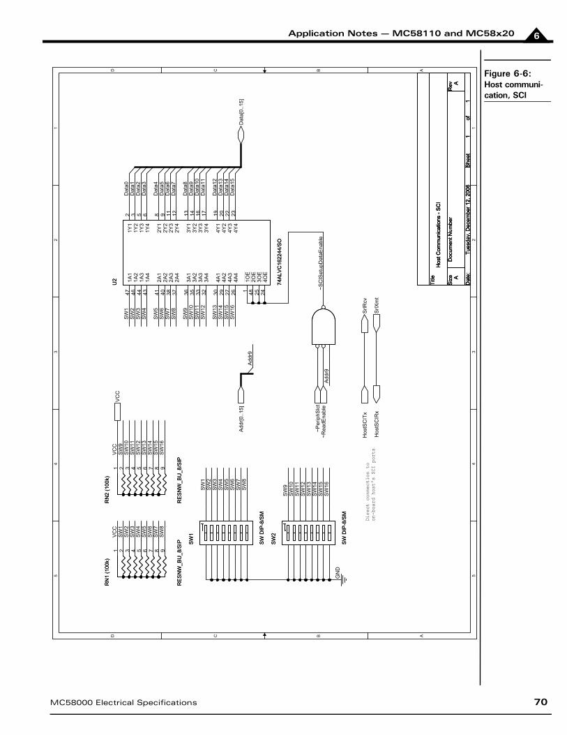
Application Notes — MC58110 and MC58x20 6
Figure 6-6:Host communi-cation, SCI
5 5
4 4
3 3
2 2
1 1
DD
CC
BB
AA
~SC
ISet
upD
ataE
nabl
e
Dat
a7
Dat
a2
Dat
a12
Dat
a6
Dat
a15
Dat
a11
Dat
a5
Dat
a9D
ata1
0
Dat
a4
Dat
a14
Dat
a1
Dat
a8
Dat
a3
Dat
a13
Dat
a0
SW
1S
W2
SW
3S
W4
SW
5S
W6
SW
7
SW
10S
W11
SW
12S
W13
SW
15S
W14
SW
9
SW
16SW
8
SW
1S
W2
SW
3S
W4
SW
7
SW
5S
W6
SW
8
VC
C
SW
11
SW
15
SW
9
SW
16
SW
14
VC
C
SW
10
SW
12S
W13
SW
1S
W2
SW
3S
W4
SW
6
SW
8
SW
5
SW
7
SW
12
SW
10S
W9
SW
11
SW
15
SW
13
SW
16
SW
14
Add
r9
GN
D
Add
r9D
ata[
0..1
5]
~Per
iphS
lct
~Rea
dEna
ble
Add
r[0..1
5]
SrlR
cvH
ostS
CIT
x
Hos
tSC
IRx
SrlX
mt
VC
C
Title
Siz
eD
ocum
ent N
umbe
rR
ev
Dat
e:S
heet
of
A
Hos
t Com
mun
icat
ions
- S
CI
A
11
Tues
day,
Dec
embe
r 12,
200
6
Title
Siz
eD
ocum
ent N
umbe
rR
ev
Dat
e:S
heet
of
A
Hos
t Com
mun
icat
ions
- S
CI
A
11
Tues
day,
Dec
embe
r 12,
200
6
Title
Siz
eD
ocum
ent N
umbe
rR
ev
Dat
e:S
heet
of
A
Hos
t Com
mun
icat
ions
- S
CI
A
11
Tues
day,
Dec
embe
r 12,
200
6
Dire
ct c
onne
ctio
n to
on
-boa
rd h
ost'
s SC
I po
rts
SW
2
SW
DIP
-8/S
M
SW
2
SW
DIP
-8/S
M
SW
1
SW
DIP
-8/S
M
SW
1
SW
DIP
-8/S
M
RN
1 (1
00k)
RE
SN
W_B
U_8
/SIP
RN
1 (1
00k)
RE
SN
W_B
U_8
/SIP
1 2 3 4 5 6 7 8 9
RN
2 (1
00k)
RE
SN
W_B
U_8
/SIP
RN
2 (1
00k)
RE
SN
W_B
U_8
/SIP
1 2 3 4 5 6 7 8 9
U2
74A
LVC
1622
44/S
O
U2
74A
LVC
1622
44/S
O
1Y1
21Y
23
1Y3
51Y
46
2Y1
82Y
29
2Y3
112Y
412
3Y1
133Y
214
3Y3
163Y
417
4Y1
194Y
220
4Y3
224Y
423
1A4
431A
344
1A2
461A
147
2A4
372A
338
2A2
402A
141
3A4
323A
333
3A2
353A
136
4A4
264A
327
4A2
294A
130
1OE
1
4OE
243O
E25
2OE
48
MC58000 Electrical Specifications 70
Application Notes — MC58110 and MC58x206
6.7.2 Interfacing to Off-board Hosts Through Asynchronous Serial CommunicationsWhen the host and motion processor are located on the same physical board it is most likely that simply wiring the transmit and receive lines directly between the host and CP chip is all that is required (assuming they are both 3.3V CMOS devices). When the host is remote and the interface requires longer communication lines, achieving reliable communication is more involved.
TIA/EIA standards provide reliable communication over varying cable lengths and communication rates. The most commonly used standards are RS-232, RS-422 and RS-485. These standards are separated into two categories: single-ended and differential. RS-232 is a single-ended standard allowing for moderate communication rates over relatively short cables. RS-422 and RS-485 are differential, offering higher data rates and longer cable runs.
Line drivers and receivers (transceivers) are commonly used in order to mediate between the cable interface and the digital circuitry signal levels. Although RS-485 transceivers also support the RS-422 electrical specification (the reverse is not true), there are several design considerations that should be taken into account when deciding which of these two communication methods is the best fit for an application.
Full-duplex vs. half-duplex
The terms full-duplex and half-duplex are used to distinguish between a system having two separate phys-ical communications lines from one having one common line for transmission and reception.
Line contention
This problem can occur in half-duplex systems. Most line-drivers supply physical protection against such conditions but there is no automatic recovery of lost data in these levels. When interfacing the Magellan to a half-duplex communication system the designer should note that the turn-around time for command processing and response is at least 1 byte at the current baud rate. As a result the host should release the communication line before this time elapses so that contention can be avoided.
Termination impedance
Long cables and/or high data rates require termination resistors if the transceiver is located at the end of the transmission lines. One way to determine if termination is required is if the propagation delay across the cable is larger than ten times the signaling transition time. If this condition is satisfied, then termination is required. The RS485 standard specifies the signaling transition time to be less than 0.3 times the signaling period, thus imposing an upper limit on the maximum cable length for a specified baud rate.
The termination resistor should match the characteristic impedance of the cable with 20% tolerance. Re-sistors with a value of 80-120 are typically used. For RS-422, only the receiver end should use a termina-tion resistor, due to the communication line being unidirectional (full duplex). Note that if the transceiver is not placed at the ends of the cable, no termination resistors are required. However, the stubs should be kept as short as possible to prevent reflections.
The schematic in Figure 6-7 employs the ADM3202 and ADM3491 transceivers as an example of RS232 and RS485/422 interfaces respectively. Other RS232 transceivers may be used, such as Maxim’s MAX3321E. The ADM3491 circuitry can be configured for both full-duplex and half-duplex communications, and may include termination resistors. As an alternative, transceivers from the MAX307xE family may be used.
The following table shows configuration options for the RS-485/422 circuitry of Figure 6-7.
Configuration Jumper Position Application
Half Duplex1 JMP1/2/3 in 2-3 RS-485 in multipoint system
Full Duplex JMP1/2/3 in 1-2 RS-422 or RS-485 in point to point system
Termination on2 JMP4/5 in 1-2 Both RS-485 and RS-422. For high transmission rates and/or long cable. Only when placed at the end of the cable.
Termination off JMP4/5 in 2-3 Both RS-485 and RS-422. For low transmission rates and short cable. Or when placed at the middle of the cable.
1. JMP3 should only be placed be in the half duplex state (2-3) if multi-point communication is being used.2. Note that the reference circuitry does not support resistance termination on the transmitting side when operated in full
duplex because it is assumed that RS 485 will only be used in the half-duplex configuration.
71 MC58000 Electrical Specifications
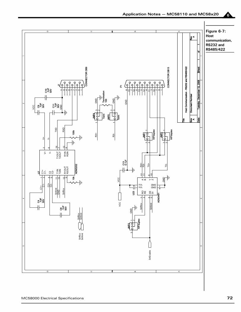
Application Notes — MC58110 and MC58x20 6
Figure 6-7:Host communication, RS232 and RS485/422
5 5
4 4
3 3
2 2
1 1
DD
CC
BB
AA
SrlR
cv
V-
V+
C1+
TXD
VC
C
C1-
C2+
SrlX
mt
RX
D
C2-
SrlX
mt
SrlR
cv
VC
C
SrlR
cvS
rlXm
t
RX
+R
X-
GN
D
GN
D
GN
D
TX+
TX-
RX
+
RX
-
GN
D
GN
D
GN
D
GN
D
SrlX
mt
SrlE
nabl
e
VC
C
SrlR
cv
Title
Siz
eD
ocum
ent N
umbe
rR
ev
Dat
e:S
heet
of
A
Hos
t Com
mun
icat
ion
- RS
232
and
RS
485/
422
A
11
Tues
day,
Dec
embe
r 12,
200
6
Title
Siz
eD
ocum
ent N
umbe
rR
ev
Dat
e:S
heet
of
A
Hos
t Com
mun
icat
ion
- RS
232
and
RS
485/
422
A
11
Tues
day,
Dec
embe
r 12,
200
6
Title
Siz
eD
ocum
ent N
umbe
rR
ev
Dat
e:S
heet
of
A
Hos
t Com
mun
icat
ion
- RS
232
and
RS
485/
422
A
11
Tues
day,
Dec
embe
r 12,
200
6
100k
100k
JMP
4
Term
JMP
4
Term
123
JMP
2
H/F
dupl
ex
JMP
2
H/F
dupl
ex123
JMP
5
Term
JMP
5
Term
12 3
10k
10k
U23
AD
M34
91U23
AD
M34
91RO
2
DI
5
RE
3
DE
4
A12
B11
Z10
Y9
Vcc13Vcc14 GND 6
GND 7
C9
.1U
F50
V
C9
.1U
F50
VC
10.1
UF
50V
C10
.1U
F50
V
J1 CO
NN
EC
TOR
DB
9
J1 CO
NN
EC
TOR
DB
9
5 9 4 8 3 7 2 6 1
P1
CO
NN
EC
TOR
DB
15
P1
CO
NN
EC
TOR
DB
15
8 15 7 14 6 13 5 12 4 11 3 10 2 9 1
U7
AD
M32
02
U7
AD
M32
02
C1+
1C
1-3
C2
4C
2-5
T1IN
11T2
IN10
R1O
UT
12R
2OU
T9
V+
2
V-
6
T1O
UT
14T2
OU
T7
R1I
N13
R2I
N8
C13
0.1u
FC
130.
1uF
C8
.1U
F50
V
C8
.1U
F50
V
JMP
3
H/F
dupl
ex
JMP
3
H/F
dupl
ex
321
C11
.1U
F50
V
C11
.1U
F50
V
C4
.1U
F50
V
C4
.1U
F50
V
JMP
1
H/F
dupl
ex
JMP
1
H/F
dupl
ex123
Term
inat
ion
100
Term
inat
ion
100
MC58000 Electrical Specifications 72

Application Notes — MC58110 and MC58x206
6.8 CAN Communication InterfaceThe following example illustrates an interface to a CAN backbone using of TI’s SN65HVD232 transceiver, which supports ISO 11898 standard. Generally the CAN high-speed standard ISO 11898 provides a single line structure as network topology. The bus line is terminated at both ends with a single termination resistor of ~120ohms. However in practice some deviation from that topology may be needed to accommodate appropriate drop cable lengths and particular applications. Consult CAN ISO 11898 standard for more information on termination schemes and EMC considerations.
6.8.1 CAN Configuration During Power-up or ResetOn power-up or after reset, the CP configures the CAN controller according to the 16-bit value residing at the peripheral address 400h. If a value of FFFFh is read, then the CAN controller is configured to its default configuration: 20 kbps with a NodeID of 0. Since the data bus inputs are internally pulled-up, the pins may remain disconnected and the default configuration will take effect at power-up or reset. If a non-default CAN configuration is required the circuitry presented in the reference schematic (Figure 6-8) may be used.
Note that after communication has been established, the CAN configuration may be altered via the SetCANMode command.
More advanced CAN bus drivers such as the SN65HVD230 supply a programmable input pin which may be used to adjust the rise and fall times of the transmitter. This may be important in unshielded, low-cost systems in order to reduce electromagnetic interference. The pin may be hard-wired through a resistor to ground (refer to the component data sheet for calculating the resistor’s value), or the host may control this pin by introducing additional circuitry attached to the I/O user space of the CP for a more flexible and tunable design.
The following should be observed when designing the power-up/reset CAN circuitry.
1 The MC58000 peripheral address map is arranged so that Addr10 is dedicated for CAN configuration.
2 The following logic condition for presenting the setup word on the data bus should be used.
~CANSetupDataEnable = ~ReadEnable + ~PeriphSlct + ~Addr10
Where:
The logic may be implemented in a PLD, and its propagation delay should not exceed 20 nsec; assuming an enable time for the tri-state buffer of less than 10 nsec.
3 The DIPswitch resistors of ~100K ensure sufficient VIH level. In case of a zero input, a current of ~33 µAwill be flowing between VCC and GND. This may result in a worst-case scenario of ~0.55 mA when theall-zero word is encoded.
~CANSetupDataEnable When high the tri-state buffer outputs are placed in a high-impedance state.
~ReadEnable When low, the bus is in a read cycle.~PeriphSlct When low, the peripheral address space is being addressed.
73 MC58000 Electrical Specifications

Application Notes — MC58110 and MC58x20 6
Figure 6-8:Host communication, CANbus
5 5
4 4
3 3
2 2
1 1
DD
CC
BB
AA
SW
1S
W2
SW
3S
W4
SW
5S
W6
SW
7
GN
D
SW
15S
W14
SW
16
SW
1S
W2
SW
3S
W4
SW
7
SW
5S
W6
VC
C
SW
15S
W16
SW
14V
CC
SW
1S
W2
SW
3S
W4
SW
6S
W5
SW
7
SW
15S
W16
SW
14
Add
r10
~CA
NS
etup
Dat
aEna
ble
SW
8G
ND
CA
NX
mt
CA
NR
cv
GN
D
CA
NH
CA
NL
Dat
a7
Dat
a2
Dat
a12
Dat
a6
Dat
a15
Dat
a11
Dat
a5
Dat
a9D
ata1
0
Dat
a4
Dat
a14
Dat
a1
Dat
a8
Dat
a3
Dat
a13
Dat
a0
Add
r10
VC
C
Dat
a[0.
.15]
Add
r[0..1
5]
~Per
iphS
lct
~Rea
dEna
ble
CA
NX
mt
CA
NR
cv
VC
C
Title
Siz
eD
ocum
ent N
umbe
rR
ev
Dat
e:S
heet
of
A
Hos
t Com
mun
icat
ion
- CA
N b
us
A
11
Tues
day,
Dec
embe
r 12,
200
6
Title
Siz
eD
ocum
ent N
umbe
rR
ev
Dat
e:S
heet
of
A
Hos
t Com
mun
icat
ion
- CA
N b
us
A
11
Tues
day,
Dec
embe
r 12,
200
6
Title
Siz
eD
ocum
ent N
umbe
rR
ev
Dat
e:S
heet
of
A
Hos
t Com
mun
icat
ion
- CA
N b
us
A
11
Tues
day,
Dec
embe
r 12,
200
6
Note: If transmitter's rise/fall times do not require adjusting
the RS pin should be tied to GND or the simpler SN65HVD232 can be
used
P2
CO
NN
EC
TOR
DB
9
P2
CO
NN
EC
TOR
DB
9
5 9 4 8 3 7 2 6 1
Slo
peC
ontro
lS
lope
Con
trol
10uF
10uF
100k
RE
SN
W_B
U_4
/SIP
100k
RE
SN
W_B
U_4
/SIP
1 2 3 4 5
SW
4
SW
DIP
-10/
SM
SW
4
SW
DIP
-10/
SM
U3
74A
LVC
1622
44/S
O
U3
74A
LVC
1622
44/S
O
1Y1
21Y
23
1Y3
51Y
46
2Y1
82Y
29
2Y3
112Y
412
3Y1
133Y
214
3Y3
163Y
417
4Y1
194Y
220
4Y3
224Y
423
1A4
431A
344
1A2
461A
147
2A4
372A
338
2A2
402A
141
3A4
323A
333
3A2
353A
136
4A4
264A
327
4A2
294A
130
1OE
1
4OE
243O
E25
2OE
48
0.1u
F0.
1uF
U4
SN
65H
VD
230
U4
SN
65H
VD
230
D1
R4
CA
NH
7
GND 2VCC3
CA
NL
6
RS
8
100k
RE
SN
W_B
U_8
/SIP
100k
RE
SN
W_B
U_8
/SIP
1 2 3 4 5 6 7 8 9
MC58000 Electrical Specifications 74
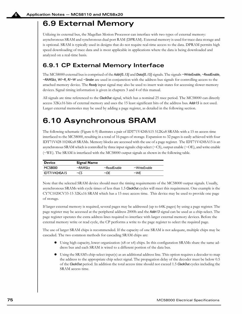
Application Notes — MC58110 and MC58x206
6.9 External MemoryUtilizing its external bus, the Magellan Motion Processor can interface with two types of external memory: asynchronous SRAM and synchronous dual port RAM (DPRAM). External memory is used for trace data storage and is optional. SRAM is typically used in designs that do not require real-time access to the data. DPRAM permits high speed downloading of trace data and is most applicable in applications where the data is being downloaded and analyzed on a real-time basis.
6.9.1 CP External Memory InterfaceThe MC58000 external bus is comprised of the Addr[0..15] and Data[0..15] signals. The signals ~WriteEnable, ~ReadEnable, ~RAMSlct, W/~R, R/~W and ~Strobe are used in conjunction with the address bus signals for controlling access to the attached memory device. The Ready input signal may also be used to insert wait-states for accessing slower memory devices. Signal timing information is given in chapters 3 and 4 of this manual.
All signals are time referenced to the ClockOut signal, which has a nominal 25 nsec period. The MC58000 can directly access 32Kx16 bits of external memory and uses the 15 least significant bits of the address bus. Addr15 is not used. Larger external memories may be used by adding a page register, as detailed in the following section.
6.10 Asynchronous SRAM The following schematic (Figure 6-9) illustrates a pair of IDT71V424SA15 512Kx8 SRAMs with a 15 ns access time interfaced to the MC58000, resulting in a total of 16 pages of storage. Expansion to 32 pages is easily achieved with four IDT71V428 1024Kx8 SRAMs. Memory blocks are accessed with the use of a page register. The IDT71V424SA15 is an asynchronous SRAM which is controlled by three input signals: chip select (~CS), output enable (~OE), and write enable
(~WE). The SRAM is interfaced with the MC58000 output signals as shown in the following table.
Note that the selected SRAM device should meet the timing requirements of the MC58000 output signals. Usually, asynchronous SRAMs with cycle times of less than 1.5 ClockOut cycles will meet this requirement. One example is the CY7C1020CV33-15 32Kx16 SRAM which has a 15 nsec access time. This device may be used to provide one page of storage.
If larger external memory is required, several pages may be addressed (up to 64K pages) by using a page register. The page register may be accessed at the peripheral address 2000h and the Addr13 signal can be used as a chip-select. The page register operates the extra address lines required to interface with larger external memory devices. Before the external memory write or read cycle, the CP performs a write to the page register to select the required page.
The use of larger SRAM chips is recommended. If the capacity of one SRAM is not adequate, multiple chips may be cascaded. The two common methods for cascading SRAM chips are:
Using high capacity, lower organization (x8 or x4) chips. In this configuration SRAMs share the same ad-dress bus and each SRAM is wired to a different portion of the data bus.
Using the SRAM’s chip-select input(s) as an additional address line. This option requires a decoder to map the address to the appropriate chip select signal. The propagation delay of the decoder must be below 0.5 of the ClockOut period. In addition the total access time should not exceed 1.5 ClockOut cycles including the SRAM access time.
Device Signal NameMC58000 ~RAMSlct ~ReadEnable ~WriteEnableIDT71V424SA15 ~CS ~OE ~WE
75 MC58000 Electrical Specifications
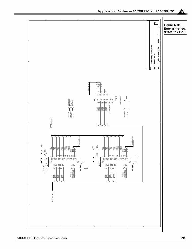
Application Notes — MC58110 and MC58x20 6
Figure 6-9:External memory, SRAM 512Kx16
5 5
4 4
3 3
2 2
1 1
DD
CC
BB
AA
VC
C
PA
15P
A16
PA
17
Add
r13
~Rea
dEna
ble
Add
r0A
ddr1
Add
r2A
ddr3
Add
r4A
ddr5
Add
r6A
ddr7
Add
r8A
ddr9
Add
r10
Add
r11
Add
r12
Add
r13
Add
r14
~Rea
dEna
ble
~Pag
eClk
Ena
ble
Add
r0A
ddr1
Add
r2A
ddr3
Add
r4A
ddr5
Add
r6A
ddr7
Add
r8A
ddr9
Add
r10
Add
r11
Add
r12
Add
r13
Add
r14
Dat
a0D
ata1
Dat
a2
~Writ
eEna
ble
~Per
iphS
lct
Dat
a3
~RA
MS
lct
~RA
MS
lct
~Per
iphS
lct
Dat
a0D
ata1
Dat
a2D
ata3
Dat
a4D
ata5
Dat
a6D
ata7
~Writ
eEna
ble
PA
18
Dat
a8D
ata9
Dat
a10
Dat
a11
Dat
a12
Dat
a13
Dat
a14
Dat
a15
~Rea
dEna
ble
~RA
MS
lct
PA
15P
A16
PA
17P
A18
PA
15P
A16
PA
17P
A18
Pag
eAdd
r[15.
.18]
Pag
eAdd
r[15.
.18]
Pag
eAdd
r[15.
.18]
Dat
a4D
ata5
Dat
a6D
ata7
~Writ
eEna
ble
~Writ
eEna
ble
VC
C
Dat
a[0.
.15]
~Writ
eEna
ble
~Rea
dEna
ble
~Per
iphS
lct
~RA
MS
lct
VC
C
Add
r[0..1
5]
Title
Siz
eD
ocum
ent N
umbe
rR
ev
Dat
e:S
heet
of
A
Ext
erna
l Mem
ory
- SR
AM
512
Kx1
6
B
11
Tues
day,
Dec
embe
r 12,
200
6
Title
Siz
eD
ocum
ent N
umbe
rR
ev
Dat
e:S
heet
of
A
Ext
erna
l Mem
ory
- SR
AM
512
Kx1
6
B
11
Tues
day,
Dec
embe
r 12,
200
6
Title
Siz
eD
ocum
ent N
umbe
rR
ev
Dat
e:S
heet
of
A
Ext
erna
l Mem
ory
- SR
AM
512
Kx1
6
B
11
Tues
day,
Dec
embe
r 12,
200
6
0.1u
F0.
1uF
U37
IDT7
1V42
4U37
IDT7
1V42
4
A0
1A
12
A2
3A
34
A4
5A
514
A6
15A
716
A8
17A
918
A10
20A
1121
A12
22A
1323
A14
24A
1532
A16
33A
1734
VDD9 VDD27VSS 10VSS 28
CS
6W
E13
OE
31A
1835
I/O1
8I/O
07
I/O2
11I/O
312
I/O4
25I/O
526
I/O6
29I/O
730
U40
74A
C37
7
U40
74A
C37
7
D0
3D
14
D2
7D
38
D4
13D
514
D6
17D
718
CLK
11
CE
1
Q0
2Q
15
Q2
6Q
39
Q4
12Q
515
Q6
16Q
719
0.1u
F0.
1uF
+4.
7uF
+4.
7uF
0.1u
F0.
1uF
U36
IDT7
1V42
4U36
IDT7
1V42
4
A0
1A
12
A2
3A
34
A4
5A
514
A6
15A
716
A8
17A
918
A10
20A
1121
A12
22A
1323
A14
24A
1532
A16
33A
1734
VDD9 VDD27VSS 10VSS 28
CS
6W
E13
OE
31A
1835
I/O1
8I/O
07
I/O2
11I/O
312
I/O4
25I/O
526
I/O6
29I/O
730
0.1u
F0.
1uF
MC58000 Electrical Specifications 76

Application Notes — MC58110 and MC58x206
6.10.1 Slow Asynchronous SRAM
If the SRAM does not meet the timing requirements, it may still be connected to the MC58000 by adding wait states. In order to generate the wait-states, the Ready signal must be activated during read/write memory accesses. As long as the Ready signal is kept low during the rising edge of the ClockOut signal, the end of the current read/write cycle will be deferred to the next ClockOut rising edge.
The following schematic (Figure 6-10) contains a circuit and timing diagram for generating one wait state. Expanding to two or more wait states is similar. Note that adding wait states slows the operation of the MC58000 and therefore the number of wait states should be kept as low as possible if the device is expected to maintain normal operation. Contact PMD to determine if the use of wait states will affect device operation in your application.
The following timing restrictions apply when the device is operating with the standard 40 MHz ClockOut frequency:-
1 tp4 + tp2 < 22 ns
2 tp2+ ts1 < 19 ns
3 tp1 + tp4 + tp3 < 9.5 ns
Where tp1 and ts1 are the propagation delay and setup time of the D flip-flop. TPx is the propagation delay of logic gate Ux.
Notes:
1 In order to meet the above timing requirements high-speed gates may be used or the logic may beimplemented in a fast PLD. Timing restriction 3 may be relaxed by the use of fast negative edge JK-FF,such as the 74LCX112, resulting in a very tight constraint on tp4.
2 If read and write cycles do not require the same number of wait states, then either ~WriteEnable or~ReadEnable may replace the ~Strobe signal. If ~ReadEnable is used, then restriction 2 becomes morestringent: tp2 + ts1 < 7.5 ns.
3 If there is no need to add wait-states the Ready input pin may be left disconnected as it is internally pulled up.
77 MC58000 Electrical Specifications
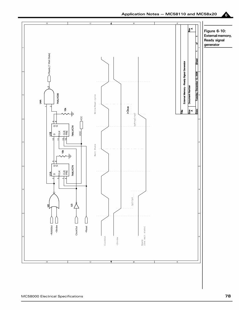
Application Notes — MC58110 and MC58x20 6
Figure 6-10:External memory, Ready signal generator
5 5
4 4
3 3
2 2
1 1
DD
CC
BB
AA
VC
C
Rea
dy [1
Wai
t Sta
te]
Clo
ckO
ut
~Stro
be
~RA
MS
lct
~Res
et
VC
C
Title
Siz
eD
ocum
ent N
umbe
rR
ev
Dat
e:S
heet
of
A
Ext
erna
l Mem
ory
- Rea
dy S
igna
l Gen
erat
or
A
11
Tues
day,
Dec
embe
r 12,
200
6
Title
Siz
eD
ocum
ent N
umbe
rR
ev
Dat
e:S
heet
of
A
Ext
erna
l Mem
ory
- Rea
dy S
igna
l Gen
erat
or
A
11
Tues
day,
Dec
embe
r 12,
200
6
Title
Siz
eD
ocum
ent N
umbe
rR
ev
Dat
e:S
heet
of
A
Ext
erna
l Mem
ory
- Rea
dy S
igna
l Gen
erat
or
A
11
Tues
day,
Dec
embe
r 12,
200
6
Cloc
kOut
~Str
obe
Read
y[O
ne w
ait
stat
e]
tp4+
tp1+
tp3
Wait
Sta
teWr
ite/
Read
cyc
le
tp2+
tp4
>3ns
U4A
74A
LVC
00
U4A
74A
LVC
00
1 23
10k
10k
10k
10k
U2
U2
U1B
74A
LVC
74
U1B
74A
LVC
74
CLR
13
D12
CLK
11
PR
E10
Q9
Q8
U1A
74A
LVC
74
U1A
74A
LVC
74
CLR
1
D2
CLK
3
PR
E4
Q5
Q6
U3
U3
MC58000 Electrical Specifications 78
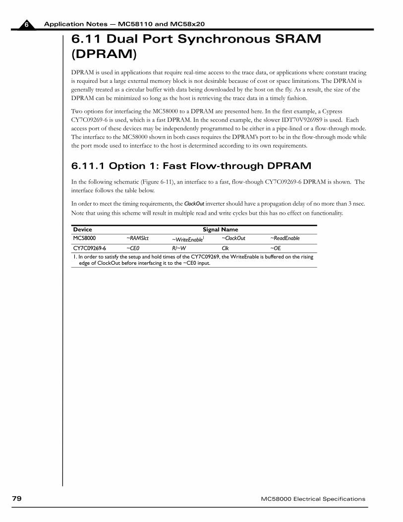
Application Notes — MC58110 and MC58x206
6.11 Dual Port Synchronous SRAM (DPRAM)DPRAM is used in applications that require real-time access to the trace data, or applications where constant tracing is required but a large external memory block is not desirable because of cost or space limitations. The DPRAM is generally treated as a circular buffer with data being downloaded by the host on the fly. As a result, the size of the DPRAM can be minimized so long as the host is retrieving the trace data in a timely fashion.
Two options for interfacing the MC58000 to a DPRAM are presented here. In the first example, a Cypress CY7C09269-6 is used, which is a fast DPRAM. In the second example, the slower IDT70V9269S9 is used. Each access port of these devices may be independently programmed to be either in a pipe-lined or a flow-through mode. The interface to the MC58000 shown in both cases requires the DPRAM’s port to be in the flow-through mode while the port mode used to interface to the host is determined according to its own requirements.
6.11.1 Option 1: Fast Flow-through DPRAM
In the following schematic (Figure 6-11), an interface to a fast, flow-though CY7C09269-6 DPRAM is shown. The interface follows the table below.
In order to meet the timing requirements, the ClockOut inverter should have a propagation delay of no more than 3 nsec.
Note that using this scheme will result in multiple read and write cycles but this has no effect on functionality.
Device Signal NameMC58000 ~RAMSlct ~WriteEnable1 ~ClockOut ~ReadEnable
CY7C09269-6 ~CE0 R/~W Clk ~OE1. In order to satisfy the setup and hold times of the CY7C09269, the WriteEnable is buffered on the rising
edge of ClockOut before interfacing it to the ~CE0 input.
79 MC58000 Electrical Specifications
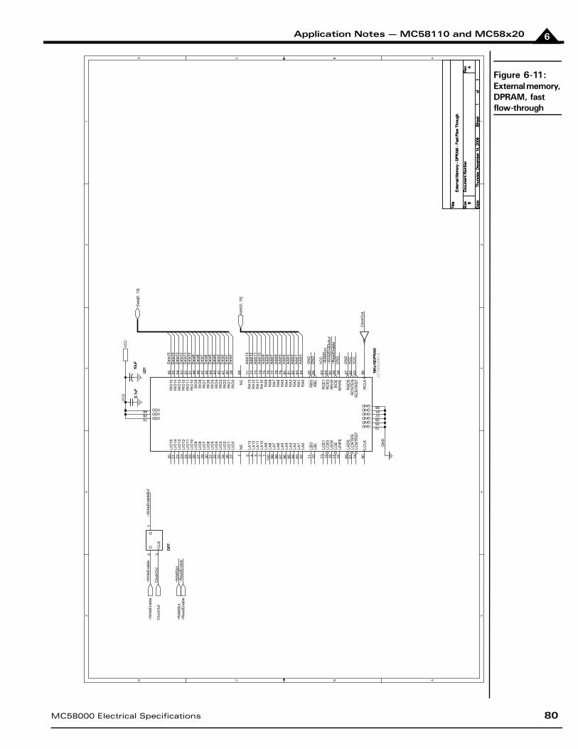
Application Notes — MC58110 and MC58x20 6
Figure 6-11:External memory, DPRAM, fast flow-through
5 5
4 4
3 3
2 2
1 1
DD
CC
BB
AA
GN
DG
ND
~Writ
eEna
bleB
uf~R
AM
Slc
t
GN
D
~Rea
dEna
ble
~RA
MS
lct
Clo
ckO
ut
GN
D
GN
D
VC
C
VC
CV
CC
VC
C
Clo
ckO
ut
~Writ
eEna
ble
~Rea
dEna
ble
~Writ
eEna
bleB
uf
Add
r5
Add
r1A
ddr2
Add
r0
Add
r13
Dat
a14
Dat
a15
Dat
a12
Dat
a13
Dat
a10
Dat
a11
Dat
a8D
ata9
Dat
a7
Dat
a5D
ata6
Dat
a3D
ata4
Dat
a1D
ata2
Dat
a0
Add
r12
Add
r10
Add
r11
Add
r8A
ddr9
Add
r7A
ddr6
Add
r3A
ddr4
VC
C
~Writ
eEna
ble
~Rea
dEna
ble
~RA
MS
lct
Clo
ckO
ut
Add
r[0..1
5]
Dat
a[0.
.15]
Title
Siz
eD
ocum
ent N
umbe
rR
ev
Dat
e:S
heet
of
A
Ext
erna
l Mem
ory
- DP
RA
M -
Fast
Flo
w T
hrou
gh
B
11
Thur
sday
, Dec
embe
r 14,
200
6
Title
Siz
eD
ocum
ent N
umbe
rR
ev
Dat
e:S
heet
of
A
Ext
erna
l Mem
ory
- DP
RA
M -
Fast
Flo
w T
hrou
gh
B
11
Thur
sday
, Dec
embe
r 14,
200
6
Title
Siz
eD
ocum
ent N
umbe
rR
ev
Dat
e:S
heet
of
A
Ext
erna
l Mem
ory
- DP
RA
M -
Fast
Flo
w T
hrou
gh
B
11
Thur
sday
, Dec
embe
r 14,
200
6
CY7C09269V-6
0.1u
F0.
1uF
10uF
10uF
DFF
DFF
Q1
D2
CLK
3
U21
16K
x16D
PR
AM
U21
16K
x16D
PR
AM
LIO
037
LIO
136
LIO
234
LIO
333
LIO
432
LIO
531
LIO
630
LIO
729
LIO
827
LIO
926
LIO
1025
LIO
1124
LIO
1223
LIO
1322
LIO
1421
LIO
1520
RIO
039
RIO
140
RIO
241
RIO
342
RIO
443
RIO
544
RIO
645
RIO
747
RIO
848
RIO
949
RIO
1051
RIO
1152
RIO
1253
RIO
1354
RIO
1455
RIO
1556
RA
183
RA
282
RA
381
RA
480
RA
579
RA
678
RA
777
RA
876
RA
975
RA
1074
RA
1173
RA
1272
RA
1371
NC
68
LA0
92LA
193
LA2
94LA
395
LA4
96LA
597
LA6
98LA
799
LA8
100
LA9
1LA
102
LA11
3LA
124
LA13
5
NC
7
LBU
11LB
L10
RB
U65
RB
L66
RC
E1
63R
CE
064
RR
/W60
RO
E59
RP
IPE
58
RC
NTE
N85
RA
DS
87
RC
NTR
ST
62
RC
LK86
LCE
113
LCE
012
LR/W
16LO
E17
LPIP
E18
LAD
S89
LCN
TEN
91LC
NTR
ST
14
LCLK
90
VDD15VDD28VDD46
GND 19GND 35GND 38GND 57GND 61GND 88
RA
084
MC58000 Electrical Specifications 80

Application Notes — MC58110 and MC58x206
This page intentionally left blank.
81 MC58000 Electrical Specifications
Application Notes — MC58110 and MC58x20 6
6.11.2 Option 2: Flow-Through with Clock Signal Control
In this example, a clock input signal is generated to the DPRAM for the ~ReadEnable and ~WriteEnable output signals.
The IDT70V9269S9 is used in a flow-through mode using the connection scheme shown in the table below.
As shown in Figure 6-12 and Figure 6-13, each MC58000 read and write cycle will generate one clock pulse, RCLK, triggering the DPRAM read/write cycle. The DslctClkIn signal is generated in order to clock the DPRAM in the event of ~RAMSlct going inactive high. Otherwise, the DPRAM will remain selected until the next read or write cycle. Other than power consumption, there is no functional effect. If power consumption is not an issue, or the bus is frequently written or read, this circuitry may be omitted.
Generating the clock for the DPRAM enables the use of lower speed DPRAM, such as the IDT70V9269S9, or the IDT70V9269S12 (as long as high-speed logic, tp < 5 ns, is used).
6.11.3 Host Interface to the DPRAM
This section provides details on the interface of a Motorola ColdFire MCF5282 microprocessor to a flow-through DPRAM. The MCF5282 utilizes several output signals for accessing external memory, including ~CSx, ~OE, R/~W, and ~TS. The MCF5282 supports a 32-bit data bus but must be configured for 16-bit words in this case. The 16 active data lines are MSBs. The address bus is designed to access bytes; thus for 16-bit word organization the LSB of the address should not be used.
The table below shows the interface to a flow-through IDT70V9269 DPRAM and requires that the following control parameters have been selected via the chip select CSCR register assigned to the DPRAM.
Auto-acknowledge enabled (AA=1)
Port size set to 16 bits
Note: The MCF5282’s ~TA and ~TAE inputs are internally pulled up, thus can remain disconnected.
In the write cycle, the latching of the data into the DPRAM must be deferred because the MCF5282 presents the data onto the bus half a clock cycle later. To generate this delay, The MCF5282 ~TS (Transfer Start) output signal is used. This signal marks the first bus clock cycle in the read/write operation and is used to keep the DPRAM deselected until valid data is presented by the MCF5282.
The MCF5282 supports a burst read/write (line transfer) mode which may be useful when downloading large trace data or when feeding an external profile.
The interface will support burst read/write cycles as long as the access cycles are internally terminated by the MCF5282 (AA=1). Note that when writing in burst mode, the first word will be written twice. This has no functional significance and is due to the 2-1-1-1 cycle pattern used by the MCF5282 in a line transfer mode.
Of importance is that the microprocessor’s BUS clock should not exceed the speed of the DPRAM. For example, for the IDT70V9269S9, the MCF5282’s BUS clock should not exceed 40 MHz.
Device Signal NameMC58000 External Logic ~RAMSlct ~WriteEnable ~ReadEnable IDT70V9269S9 RCLK ~CE0 R/~W ~OE
Device SignalMCF5282 IA[1:14] ID[16:31] ~CS1 R/~W ~TS+R/~W ~OE IDT70V9269 A[0..13] D[0:15] ~CE0 R/~W CE1 ~OE
MC58000 Electrical Specifications 82
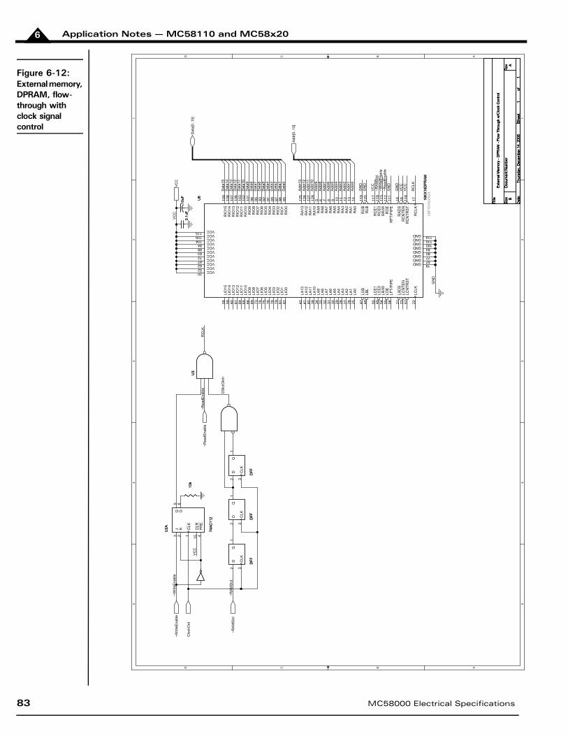
Application Notes — MC58110 and MC58x206
Figure 6-12:External memory, DPRAM, flow-through with clock signal control
5 5
4 4
3 3
2 2
1 1
DD
CC
BB
AA
GN
D
VC
C
GN
D
~Writ
eEna
ble
~Rea
dEna
ble
VC
CG
ND
VC
C
GN
D
RC
LK
~RA
MS
lct
GN
D
VC
C
Add
r5
Add
r1A
ddr2
Add
r0
Add
r13
Dat
a14
Dat
a15
Dat
a12
Dat
a13
Dat
a10
Dat
a11
Dat
a8D
ata9
Dat
a7
Dat
a5D
ata6
Dat
a3D
ata4
Dat
a1D
ata2
Dat
a0
Add
r12
Add
r10
Add
r11
Add
r8A
ddr9
Add
r7A
ddr6
Add
r3A
ddr4
~Rea
dEna
ble
VC
C
~Writ
eEna
ble
~RA
MS
lct
DS
lctC
lkIn
RC
LK
VC
C
Add
r[0..1
5]
Dat
a[0.
.15]
~Writ
eEna
ble
~Rea
dEna
ble
Clo
ckO
ut
~RA
MS
lct
Title
Siz
eD
ocum
ent N
umbe
rR
ev
Dat
e:S
heet
of
A
Ext
erna
l Mem
ory
- DP
RA
M -
Flow
Thr
ough
w/C
lock
Con
trol
B
11
Thur
sday
, Dec
embe
r 14,
200
6
Title
Siz
eD
ocum
ent N
umbe
rR
ev
Dat
e:S
heet
of
A
Ext
erna
l Mem
ory
- DP
RA
M -
Flow
Thr
ough
w/C
lock
Con
trol
B
11
Thur
sday
, Dec
embe
r 14,
200
6
Title
Siz
eD
ocum
ent N
umbe
rR
ev
Dat
e:S
heet
of
A
Ext
erna
l Mem
ory
- DP
RA
M -
Flow
Thr
ough
w/C
lock
Con
trol
B
11
Thur
sday
, Dec
embe
r 14,
200
6
IDT70V9269S9
DFF
DFF
Q1
D2
CLK
3
DFF
DFF
Q1
D2
CLK
3
U2A
74A
C11
2
U2A
74A
C11
2
Q5
Q6
J3
K2
CLK
1
PR
E4
CLR
15
DFF
DFF
Q1
D2
CLK
3
U3
U3
10k
10k
0.1u
F0.
1uF
10uF
10uF U
6
16K
X16
DP
RA
M
U6
16K
X16
DP
RA
M
LIO
082
LIO
181
LIO
279
LIO
378
LIO
476
LIO
575
LIO
674
LIO
773
LIO
869
LIO
966
LIO
1065
LIO
1164
LIO
1261
LIO
1360
LIO
1459
LIO
1558
RIO
085
RIO
186
RIO
287
RIO
389
RIO
491
RIO
592
RIO
693
RIO
795
RIO
898
RIO
910
1R
IO10
102
RIO
1110
3R
IO12
106
RIO
1310
7R
IO14
108
RIO
1510
9
RA
014
RA
113
RA
212
RA
311
RA
410
RA
59
RA
68
RA
77
RA
86
RA
95
RA
1012
8R
A11
127
RA
1212
6R
A13
125
LA0
25LA
126
LA2
27LA
328
LA4
29LA
530
LA6
31LA
732
LA8
33LA
934
LA10
39LA
1140
LA12
41LA
1342
LUB
47LB
L48
RU
B11
9R
LB12
0
RC
E1
117
RC
E0
118
RR
/W11
3R
OE
112
RC
NTE
N16
RA
DS
18
RC
NTR
ST
116
RC
LK17
LCE
150
LCE
049
LR/W
54LO
E55
LAD
S21
LCN
TEN
23LC
NTR
ST
51
LCLK
22
VCC20
GND 19
RFT
/PIP
E11
1LF
T/P
IPE
56
VCC52VCC62VCC67VCC72VCC83VCC88VCC94VCC104VCC105VCC115
GND 57GND 77GND 80GND 84GND 100GND 110GND 114
83 MC58000 Electrical Specifications

Application Notes — MC58110 and MC58x20 6
Figure 6-13:External memory, DPRAM, RCLK timing
5 5
4 4
3 3
2 2
1 1
DD
CC
BB
AA
VC
C
DS
lctC
lkIn
~Writ
eEna
ble
~Rea
dEna
ble
Clo
ckO
ut
~RA
MS
lct
RC
LK
Title
Siz
eD
ocum
ent N
umbe
rR
ev
Dat
e:S
heet
of
A
Ext
erna
l Mem
ory
- DP
RA
M -
RC
LK ti
min
g
B
11
Thur
sday
, Dec
embe
r 28,
200
6
Title
Siz
eD
ocum
ent N
umbe
rR
ev
Dat
e:S
heet
of
A
Ext
erna
l Mem
ory
- DP
RA
M -
RC
LK ti
min
g
B
11
Thur
sday
, Dec
embe
r 28,
200
6
Title
Siz
eD
ocum
ent N
umbe
rR
ev
Dat
e:S
heet
of
A
Ext
erna
l Mem
ory
- DP
RA
M -
RC
LK ti
min
g
B
11
Thur
sday
, Dec
embe
r 28,
200
6
DFF
DFF
Q1
D2
CLK
3
U2A
74A
C11
2
U2A
74A
C11
2
Q5
Q6
J3
K2
CLK
1
PR
E4
CLR
15
DFF
DFF
Q1
D2
CLK
3
DFF
DFF
Q1
D2
CLK
3
10k
10k
U3
U3
U1
U1
adEn
able
eR ~
tcl SM AR~
tc lSMAR~
ETIRW
elb anE etirW ~
tuOkcolC
K LCR
K LCR
3pt
3pt+2p t
+2 pt3 pt
es -eDgnitcel
MAR tc eles-eD
ataD]51.. 0[
1DCt
DA
ER
a taD]51.. 0[
MC58000 Electrical Specifications 84

Application Notes — MC58110 and MC58x206
6.11.4 Host DPRAM ManagementWhenever data trace is in operation, the host must monitor the RAM in order to prevent overwrites. This is generally accomplished using timers to poll the MC58000 address pointer at regular intervals. It may also be assisted with the use of an external interrupt that indicates the condition of the RAM. The schematic in Figure 6-14 includes an example for generating a signal based upon Addr12 from the MC58000. It will generate a rising edge periodic interrupt whenever the DPRAM is being written to in the 1000h and 3000h address blocks, allowing the DPRAM to be half filled in between interrupts.
6.12 Using the On-chip ADCIn this section two types of conditioning circuits which interface to the on-chip analog-to-digital converter are demonstrated. The first circuit interfaces to a single-ended voltage signal, and the second circuit to a differential voltage signal. The conditioning circuits should be adjusted appropriately in order to meet the system’s requirements.
The MC58000 is equipped with an eight-channel 10-bit ADC. The sampling rate of each channel is 57.8K samples per second, and the sample-and-hold time per channel is 1.6 µsec. The sampling capacitor is 30 pF, and the sampling resistor is in the range of 100 - 200 . In order to meet the timing requirements, the output impedance of the conditioning circuitry, as seen by the ADC’s inputs, should not exceed 6.1 k .
The digital value derived from the input analog voltage is determined using the following formula.
Digital value = 1023 x (input voltage - VREFLO) / (VREFHI - VREFLO) (1)
Where VREFLO and VREFHI are the voltages applied at AnalogRefLow and AnalogRefHigh pins, respectively.
The ADC’s performance is guaranteed when VREFLO = AGND and VREFHI = AVCC. Not adhering to these values
may result in performance degradation.
The ADC power supply should be decoupled with the use of a 2.2-6.8 µF tantalum capacitor in parallel with a 0.01-0.1 µF ceramic capacitor placed as closely as possible to the power supply and ground pins. An additional 0.01-0.1 µF ceramic capacitor should be placed across AnalogRefLow and AnalogRefHigh.
85 MC58000 Electrical Specifications
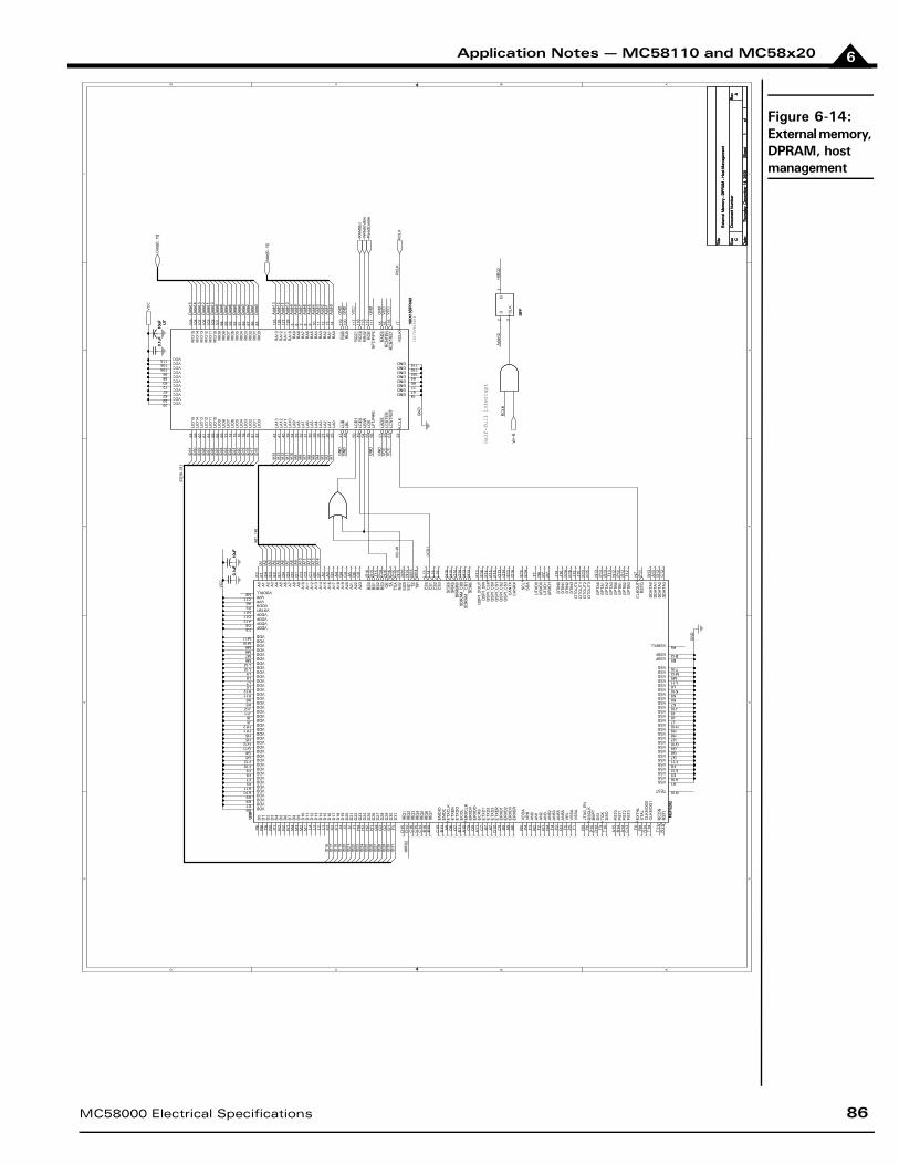
Application Notes — MC58110 and MC58x20 6
Figure 6-14:External memory, DPRAM, host management
5 5
4 4
3 3
2 2
1 1
DD
CC
BB
AA
GN
D
IA3
IA4
IA2
IA1
IA13
IA12
IA10
IA11
IA9
IA8
IA7
IA5
IA6
HIR
Q2
ID26
ID29
ID25
ID17
ID18
ID30
ID27
ID22
ID16
ID21
ID20
ID31
ID24
ID19
ID28
ID23
IR/~
W
HIR
Q2
~IC
S1
IA3
IA2
IA4
IA1
IA[1
..14]
IA13
IA14
IA12
IA9
IA11
IA10
IA7
IA8
IA6
IA5
ID[1
6..3
1]
ID31
ID30
ID29
ID28
ID26
ID27
ID25
ID24
ID23
ID22
ID20
ID21
ID19
ID18
ID16
ID17
IA14
GN
DG
ND
GN
D
GN
D
Addr
5
Addr
1Ad
dr2
Addr
0
GN
D
VCC
GN
D
VCC
GN
D
VCC
GN
D
Addr
13
RC
LK
Dat
a14
Dat
a15
Dat
a12
Dat
a13
Dat
a10
Dat
a11
Dat
a8D
ata9
Dat
a7
Dat
a5D
ata6
Dat
a3D
ata4
Dat
a1D
ata2
Dat
a0
Addr
12
Addr
10Ad
dr11
Addr
8Ad
dr9
Addr
7Ad
dr6
Addr
3Ad
dr4
GN
D
VCC
VCC
VCC
Addr
12R
CLK
Addr
[0..1
5]
~Writ
eEna
ble
~Rea
dEna
ble
RC
LK
~RAM
Slct
VCC
Dat
a[0.
.15]
W/~
R
Title
Size
Doc
umen
t Num
ber
Rev
Dat
e:Sh
eet
of
A
Exte
rnal
Mem
ory
- DPR
AM -
Hos
t Man
agem
ent
C
11
Thur
sday
, Dec
embe
r 14,
200
6
Title
Size
Doc
umen
t Num
ber
Rev
Dat
e:Sh
eet
of
A
Exte
rnal
Mem
ory
- DPR
AM -
Hos
t Man
agem
ent
C
11
Thur
sday
, Dec
embe
r 14,
200
6
Title
Size
Doc
umen
t Num
ber
Rev
Dat
e:Sh
eet
of
A
Exte
rnal
Mem
ory
- DPR
AM -
Hos
t Man
agem
ent
C
11
Thur
sday
, Dec
embe
r 14,
200
6
IDT7
0V92
69S9
Half-full interrupt
U30 MC
F528
2
U30 MC
F528
2
D0
P6
D1
R6
D2
T6D
3N
5D
4P
1D
5N
3D
6N
2D
7N
1D
8M
4D
9M
3D
10M
2D
11M
1D
12L4
D13
L3D
14L2
D15
L1D
16K
3D
17K
2D
18K
1D
19J4
D20
J3D
21J2
D22
J1D
23H
4D
24H
3D
25H
2D
26H
1D
27G
4D
28G
3D
29G
2D
30G
1D
31F3
A0
F2A
1F1
A2
E4
A3
E3
A4
E2
A5
E1
A6
D4
A7
D3
A8
D2
A9
D1
A10
C3
A11
C2
A12
C1
A13
B2
A14
B1
A15
A2
A16
A3
A17
B3
A18
A4
A19
B4
A20
C4
A21
A5
A22
B6
A23
C6
VDDE6VDDE7VDDE8VDDE9VDDE10VDDE11
VDDF7VDDF8VDDF9VDDF10VDDF12VDDG5VDDG6VDDG11VDDG12VDDH5VDDH6VDDH11VDDH12VDDJ5VDDJ6VDDJ11VDDJ12VDDK5VDDK6VDDK11VDDK12VDDL5VDDL7VDDL8VDDL9VDDL10VDDL12VDDM6VDDM7VDDM8VDDM9VDDM10VDDM11
VDDFC5
VDDFA12 VDDFD5
VDDFD11VSTBYN11
VPPC11
BS
0R
16B
S1
R15
BS
2T1
5B
S3
P14
OE
N16
TAP
16TE
AP
15R
/WN
15S
IZ0
M16
SIZ
1N
14TS
M15
TIP
M14
CS
0L1
3C
S1
L14
CS
2L1
5C
S3
L16
SC
AS
H16
SR
AS
H15
DR
AM
WG
15S
DR
AM
_CS
0G
16S
DR
AM
__C
S1
H13
SC
KE
H14
IRQ
1D
15IR
Q2
D14
IRQ
3C
16IR
Q4
C15
IRQ
5C
14IR
Q6
B16
IRQ
7B
15
EM
DIO
C10
EM
DC
B10
ETX
CLK
A8
ETX
EN
D6
ETX
DO
D7
EC
OL
B11
ER
XC
LKA
10E
RX
DV
C8
ER
XD
OD
9E
CR
SA
11
ETX
ER
D10
ER
XE
RB
8
ETX
D1
C7
ETX
D2
B7
ETX
D3
A7
ER
XD
1C
9E
RX
D2
B9
ER
XD
3A
9
QS
PI_
DO
UT
F13
QS
PI_
DIN
E16
QS
PI_
CLK
F14
QS
PI_
CS
0F1
5Q
SP
I_C
S1
F16
QS
PI_
CS
2G
13Q
SP
I_C
S3
G14
CA
NTX
E13
CA
NR
XD
16
SC
LE
15S
DA
E14
UTX
D0
T7
UTX
D1
P7
UR
XD
0N
6
UR
XD
1R
7
DTI
N0
J14
DTI
N1
J16
DTI
N2
K14
DTI
N3
K16
DTO
UT0
J13
DTO
UT1
J15
DTO
UT2
K13
DTO
UT3
K15
GP
TA0
N13
GP
TA1
P13
GP
TA2
R13
GP
TA3
T13
GP
TB0
N12
GP
TB1
P12
GP
TB2
R12
GP
TB3
T12
AN
0T3
AN
1R
2A
N2
T2A
N3
R1
AN
52R
4A
N53
T4A
N55
P3
AN
56R
3
VD
DA
R5
VR
HP
4
VR
LT5
VS
SA
P5
JTA
G_E
NR
9D
SC
LKP
9B
KP
TP
10D
SI
R10
TCK
T9
DD
ATA
0B
13D
DA
TA1
A13
DD
ATA
2D
12D
DA
TA3
C12
PS
T0A
15P
ST1
B14
PS
T2A
14P
ST3
C13
VDDPLLN8
RS
TIR
11
RS
TOP
11E
XTA
LT8
CLK
OU
TN
7
CLK
MO
D0
R14
CLK
MO
D1
T14
RC
ON
T11
DS
OT1
0
TEST N10
XTA
LR
8
VSS A1VSS A16
VSS G7VSS G8VSS G9VSS G10VSS H7VSS H8VSS H9VSS H10VSS J7VSS J8VSS J9VSS J10VSS K7VSS K8VSS K9VSS K10VSS L6VSS L11
VSS E5VSS E12VSS F6VSS F11
VSS M5VSS M12VSS T16
VSSPLL P8
VDDHP2
VS
SA
T1
VPPA6
VSSF B5VSSF B12
VDDF5
10uF
10uF
DFF
DFF
Q1
D2
CLK
3
0.1u
F0.
1uF
0.1u
F0.
1uF
U7
16KX
16D
PRAM
U7
16KX
16D
PRAM
LIO
082
LIO
181
LIO
279
LIO
378
LIO
476
LIO
575
LIO
674
LIO
773
LIO
869
LIO
966
LIO
1065
LIO
1164
LIO
1261
LIO
1360
LIO
1459
LIO
1558
RIO
085
RIO
186
RIO
287
RIO
389
RIO
491
RIO
592
RIO
693
RIO
795
RIO
898
RIO
910
1R
IO10
102
RIO
1110
3R
IO12
106
RIO
1310
7R
IO14
108
RIO
1510
9
RA
014
RA
113
RA
212
RA
311
RA
410
RA
59
RA
68
RA
77
RA
86
RA
95
RA
1012
8R
A11
127
RA
1212
6R
A13
125
LA0
25LA
126
LA2
27LA
328
LA4
29LA
530
LA6
31LA
732
LA8
33LA
934
LA10
39LA
1140
LA12
41LA
1342
LUB
47LB
L48
RU
B11
9R
LB12
0
RC
E1
117
RC
E0
118
RR
/W11
3R
OE
112
RC
NTE
N16
RA
DS
18
RC
NTR
ST
116
RC
LK17
LCE
150
LCE
049
LR/W
54LO
E55
LAD
S21
LCN
TEN
23LC
NTR
ST
51
LCLK
22
VCC20
GND 19
RFT
/PIP
E11
1LF
T/P
IPE
56
VCC52VCC62VCC67VCC72VCC83VCC88VCC94VCC104VCC105VCC115
GND 57GND 77GND 80GND 84GND 100GND 110GND 114
10uF
10uF
MC58000 Electrical Specifications 86
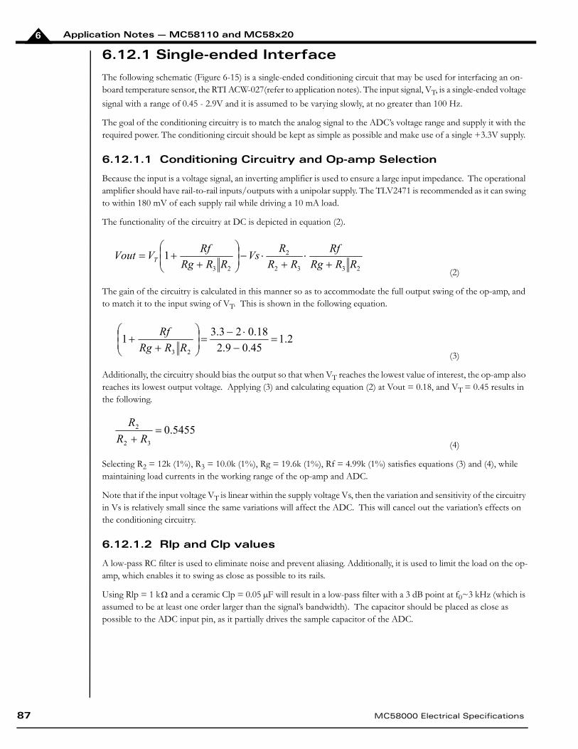
Application Notes — MC58110 and MC58x206
6.12.1 Single-ended Interface
The following schematic (Figure 6-15) is a single-ended conditioning circuit that may be used for interfacing an on-board temperature sensor, the RTI ACW-027(refer to application notes). The input signal, VT, is a single-ended voltage
signal with a range of 0.45 - 2.9V and it is assumed to be varying slowly, at no greater than 100 Hz.
The goal of the conditioning circuitry is to match the analog signal to the ADC’s voltage range and supply it with the required power. The conditioning circuit should be kept as simple as possible and make use of a single +3.3V supply.
6.12.1.1 Conditioning Circuitry and Op-amp Selection
Because the input is a voltage signal, an inverting amplifier is used to ensure a large input impedance. The operational amplifier should have rail-to-rail inputs/outputs with a unipolar supply. The TLV2471 is recommended as it can swing to within 180 mV of each supply rail while driving a 10 mA load.
The functionality of the circuitry at DC is depicted in equation (2).
(2)
The gain of the circuitry is calculated in this manner so as to accommodate the full output swing of the op-amp, and to match it to the input swing of VT. This is shown in the following equation.
(3)
Additionally, the circuitry should bias the output so that when VT reaches the lowest value of interest, the op-amp also reaches its lowest output voltage. Applying (3) and calculating equation (2) at Vout = 0.18, and VT = 0.45 results in the following.
(4)
Selecting R2 = 12k (1%), R3 = 10.0k (1%), Rg = 19.6k (1%), Rf = 4.99k (1%) satisfies equations (3) and (4), while maintaining load currents in the working range of the op-amp and ADC.
Note that if the input voltage VT is linear within the supply voltage Vs, then the variation and sensitivity of the circuitry in Vs is relatively small since the same variations will affect the ADC. This will cancel out the variation’s effects on the conditioning circuitry.
6.12.1.2 Rlp and Clp values
A low-pass RC filter is used to eliminate noise and prevent aliasing. Additionally, it is used to limit the load on the op-amp, which enables it to swing as close as possible to its rails.
Using Rlp = 1 k and a ceramic Clp = 0.05 µF will result in a low-pass filter with a 3 dB point at f0~3 kHz (which is assumed to be at least one order larger than the signal’s bandwidth). The capacitor should be placed as close as possible to the ADC input pin, as it partially drives the sample capacitor of the ADC.
2332
2
23
1RRRg
Rf
RR
RVs
RRRg
RfVVout T
2.145.09.2
18.023.31
23
RRRg
Rf
5455.032
2 RR
R
87 MC58000 Electrical Specifications
Application Notes — MC58110 and MC58x20 6
Figure 6-15:ADC, single-ended temperature sensor
5 5
4 4
3 3
2 2
1 1
DD
CC
BB
AA
VT
+3.3
Vs
VT
Vs
Vou
t
+3.3
Vs
Ana
log0
Title
Siz
eD
ocum
ent N
umbe
rR
ev
Dat
e:S
heet
of
A
AD
C -
Sin
gle-
End
ed T
empe
ratu
re S
enso
r
A
11
Tues
day,
Dec
embe
r 12,
200
6
Title
Siz
eD
ocum
ent N
umbe
rR
ev
Dat
e:S
heet
of
A
AD
C -
Sin
gle-
End
ed T
empe
ratu
re S
enso
r
A
11
Tues
day,
Dec
embe
r 12,
200
6
Title
Siz
eD
ocum
ent N
umbe
rR
ev
Dat
e:S
heet
of
A
AD
C -
Sin
gle-
End
ed T
empe
ratu
re S
enso
r
A
11
Tues
day,
Dec
embe
r 12,
200
6
Thermistor example
R1
20.0
kR
120
.0k
R3
10.0
kR
310
.0k
Rf
4.99
kR
f4.
99k
0.01
uF0.
01uF
tRT
AC
W-0
27
tRT
AC
W-0
27
Clp
0.04
7uF
Clp
0.04
7uF
Rg
19.6
kR
g19
.6k
0.01
uF0.
01uF
R2
12.0
kR
212
.0k
-+
U1
TLV
2471
-+
U1
TLV
2471
3
2
41
5
Rlp 1k
Rlp 1k
MC58000 Electrical Specifications 88
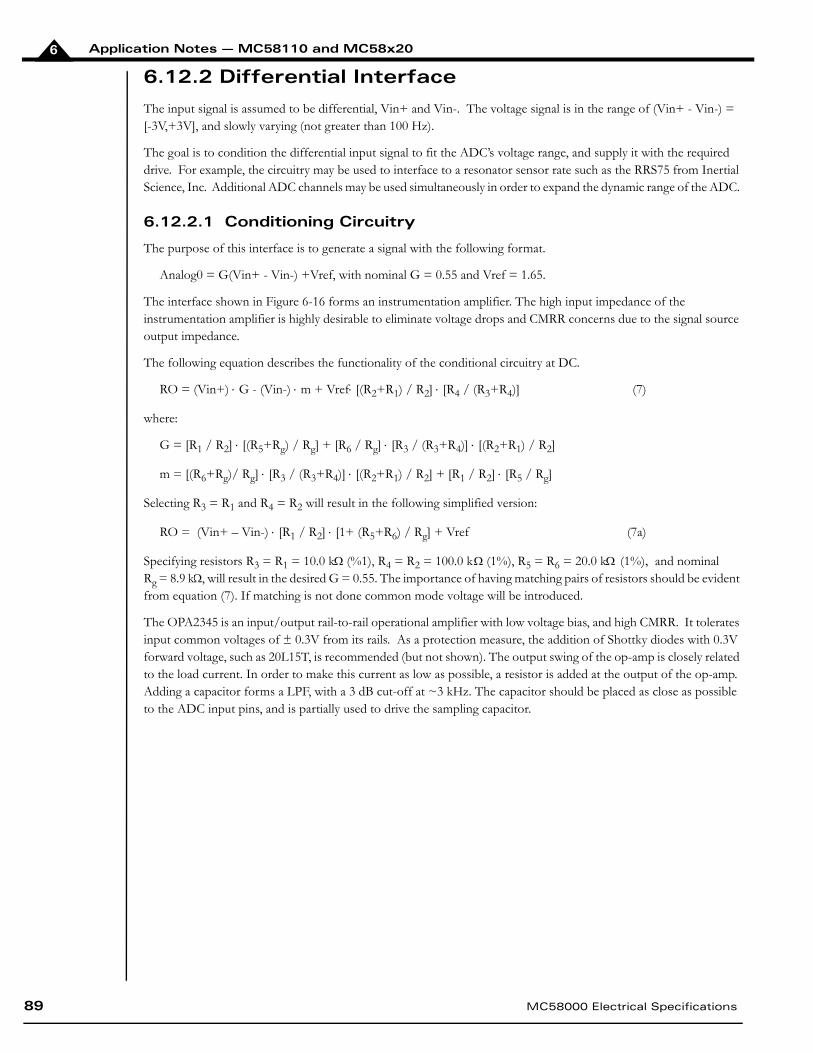
Application Notes — MC58110 and MC58x206
6.12.2 Differential Interface
The input signal is assumed to be differential, Vin+ and Vin-. The voltage signal is in the range of (Vin+ - Vin-) = [-3V,+3V], and slowly varying (not greater than 100 Hz).
The goal is to condition the differential input signal to fit the ADC’s voltage range, and supply it with the required drive. For example, the circuitry may be used to interface to a resonator sensor rate such as the RRS75 from Inertial Science, Inc. Additional ADC channels may be used simultaneously in order to expand the dynamic range of the ADC.
6.12.2.1 Conditioning Circuitry
The purpose of this interface is to generate a signal with the following format.
Analog0 = G(Vin+ - Vin-) +Vref, with nominal G = 0.55 and Vref = 1.65.
The interface shown in Figure 6-16 forms an instrumentation amplifier. The high input impedance of the instrumentation amplifier is highly desirable to eliminate voltage drops and CMRR concerns due to the signal source output impedance.
The following equation describes the functionality of the conditional circuitry at DC.
RO = (Vin+) G - (Vin-) m + Vref [(R2+R1) / R2] [R4 / (R3+R4)] (7)
where:
G = [R1 / R2] [(R5+Rg) / Rg] + [R6 / Rg] [R3 / (R3+R4)] [(R2+R1) / R2]
m = [(R6+Rg)/ Rg] [R3 / (R3+R4)] [(R2+R1) / R2] + [R1 / R2] [R5 / Rg]
Selecting R3 = R1 and R4 = R2 will result in the following simplified version:
RO = (Vin+ – Vin-) [R1 / R2] [1+ (R5+R6) / Rg] + Vref (7a)
Specifying resistors R3 = R1 = 10.0 k (%1), R4 = R2 = 100.0 k (1%), R5 = R6 = 20.0 k (1%), and nominal Rg = 8.9 k , will result in the desired G = 0.55. The importance of having matching pairs of resistors should be evident from equation (7). If matching is not done common mode voltage will be introduced.
The OPA2345 is an input/output rail-to-rail operational amplifier with low voltage bias, and high CMRR. It tolerates input common voltages of ± 0.3V from its rails. As a protection measure, the addition of Shottky diodes with 0.3V forward voltage, such as 20L15T, is recommended (but not shown). The output swing of the op-amp is closely related to the load current. In order to make this current as low as possible, a resistor is added at the output of the op-amp. Adding a capacitor forms a LPF, with a 3 dB cut-off at ~3 kHz. The capacitor should be placed as close as possible to the ADC input pins, and is partially used to drive the sampling capacitor.
89 MC58000 Electrical Specifications
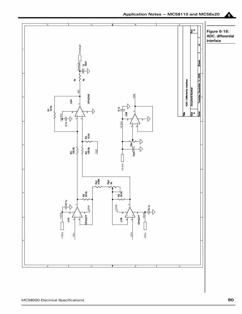
Application Notes — MC58110 and MC58x20 6
Figure 6-16:ADC, differential interface
5 5
4 4
3 3
2 2
1 1
DD
CC
BB
AA
+3.3
Vs
RO
Vin
+
-15V
S
+15V
S
Vre
f
Vre
f
Vin
-
+3.3
Vs
+15V
S
-15V
S
Ana
log0
+3.3
Vs
+15V
s
-15V
s
Ana
log0
Title
Siz
eD
ocum
ent N
umbe
rR
ev
Dat
e:S
heet
of
A
AD
C /
Diff
eren
tial I
nter
face
A
11
Tues
day,
Dec
embe
r 12,
200
6
Title
Siz
eD
ocum
ent N
umbe
rR
ev
Dat
e:S
heet
of
A
AD
C /
Diff
eren
tial I
nter
face
A
11
Tues
day,
Dec
embe
r 12,
200
6
Title
Siz
eD
ocum
ent N
umbe
rR
ev
Dat
e:S
heet
of
A
AD
C /
Diff
eren
tial I
nter
face
A
11
Tues
day,
Dec
embe
r 12,
200
6
Rl
4kRl
4kR
520
.0k
R5
20.0
k
- +
U1B
OP
A22
77
- +
U1B
OP
A22
77
4
756
8
R3
10.0
kR
310
.0k
R1
10.0
kR
110
.0k
R4
100.
0kR
410
0.0k
10uF
10uF
0.1u
0.1u
-+
U2A
OP
A23
45
-+
U2A
OP
A23
45
23
48
1
20k
20k
R2
100.
0kR
210
0.0k
Cl
15nF
Cl
15nF
Rg1
4.99
kR
g14.
99k
R6
20.0
kR
620
.0k
-+
U2B
-+
U2B
65
48
7
0.1u
0.1u
Rg2
5kRg2
5k
0.1u
0.1u
-+
U1A
OP
A22
77-+
U1A
OP
A22
77
4
13 2
8
0.1u
0.1u
MC58000 Electrical Specifications 90
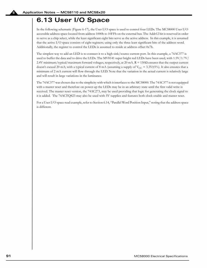
Application Notes — MC58110 and MC58x206
6.13 User I/O SpaceIn the following schematic (Figure 6-17), the User I/O space is used to control four LEDs. The MC58000 User I/O accessible address space located from address 1000h to 10FFh on the external bus. The Addr12 bit is reserved in order to serve as a chip select, while the least significant eight bits serve as the active address. In this example, it is assumed that the active I/O space consists of eight registers; using only the three least significant bits of the address word. Additionally, the register to control the LEDs is assumed to reside at address offset 0x7h.
The simplest way to add an LED is to connect it to a high sink/source current port. In this example, a 74AC377 is used to buffer the data and to drive the LEDs. The MV8141 super bright red LEDs have been used, with 1.5V/1.7V/2.4V minimum/typical/maximum forward voltages, respectively, at 20 mA. R = 150 ensures that the output current doesn’t exceed 20 mA; with a typical current of 8 mA (assuming a supply of VCC = 3.3V5%). It also ensures that a minimum of 2 mA current will flow through the LED. Note that the variation in the actual current is relatively large and will result in large variations in the luminance.
The 74AC377 was chosen due to the simplicity with which it interfaces to the MC58000. The 74AC377 is not equipped with a master reset and therefore on power-up the LEDs may be in an arbitrary state until the first valid write is received. The master reset version, the 74AC273, may be used providing that logic for generating the clock signal to it is added. The 74ACTQ823 may also be used with 5V supplies and features both clock enable and master reset.
For a User I/O space read example, refer to Section 6.14, “Parallel Word Position Input,” noting that the address space is different.
91 MC58000 Electrical Specifications
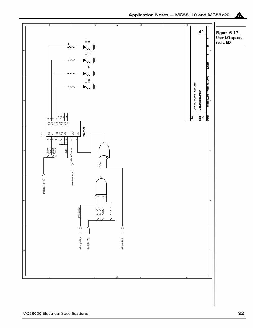
Application Notes — MC58110 and MC58x20 6
Figure 6-17:User I/O space, red L ED
5 5
4 4
3 3
2 2
1 1
DD
CC
BB
AA
~Per
iphS
lct
Add
r0A
ddr1
Add
r2
Add
r12
Dat
a1
~Writ
eEna
ble
~CS
led
Dat
a3D
ata2
Dat
a0
GN
D
~Res
etH
old
~Per
iphS
lct
Add
r[0..1
5]
~Writ
eEna
ble
Dat
a[0.
.15]
Title
Siz
eD
ocum
ent N
umbe
rR
ev
Dat
e:S
heet
of
A
Use
r I/O
Spa
ce -
Red
LE
D
A
11
Tues
day,
Dec
embe
r 12,
200
6
Title
Siz
eD
ocum
ent N
umbe
rR
ev
Dat
e:S
heet
of
A
Use
r I/O
Spa
ce -
Red
LE
D
A
11
Tues
day,
Dec
embe
r 12,
200
6
Title
Siz
eD
ocum
ent N
umbe
rR
ev
Dat
e:S
heet
of
A
Use
r I/O
Spa
ce -
Red
LE
D
A
11
Tues
day,
Dec
embe
r 12,
200
6
D1
LED
D1
LED
D2
LED
D2
LED
RR
1
2 3 4 5 6
U11
74A
C37
7
U11
74A
C37
7
D0
3D
14
D2
7D
38
D4
13D
514
D6
17D
718
CLK
11
CE
1
Q0
2Q
15
Q2
6Q
39
Q4
12Q
515
Q6
16Q
719
D3
LED
D3
LED
D0
LED
D0
LED
MC58000 Electrical Specifications 92
Application Notes — MC58110 and MC58x206
6.14 Parallel Word Position InputThe following schematic (Figure 6-18) shows an interface to the AD2S1200 in order to generate a digital word position feedback input to the MC58000. The AD2S1200 is a programmable 12-bit resolution resolver-to-digital converter. In the following example, the digital interface to the CP’s data bus will be demonstrated. The motor interface to the resolver is not shown. The MC58000 maps the peripheral addresses 800h, 801h, 802h, and 803h to the position input registers for axes 1 to 4, respectively. For the MC58110 only address 800h is used.
The interface to the AD2S1200 uses the MC58000’s output signal, Synch. A falling edge of the Synch signal indicates that a position inputs are to be read. The rising edge of this signal is used to sample the resolver’s position. The actual reads of these values occurs only one cycle later, introducing effective delay of one cycle (51.2 µsec for a 40 MHz IOClkIn/20 MHz CPClkIn). This delay is necessary to guarantee the timing requirement of the AD2S1200. Consult PMD for ways to avoid this delay.
Note that the Synch signal should be activated using the SetSynchronizationMode command.
The TTL outputs of the AD2S1200 are interfaced to a common 3.3V LVT family’s 16-bit buffer. The LVT family is a low voltage CMOS with TTL compatible inputs and an input VHI tolerance of up to 5.5V.
Note that the decoder is required only when parallel word input is used by more than one axis. If only one or two axes are used, it is simpler to generate the chip-select signals using discrete components.
93 MC58000 Electrical Specifications

Application Notes — MC58110 and MC58x20 6
Figure 6-18:Parallel word feedback, AD2S1200, 4 axes
5 5
4 4
3 3
2 2
1 1
DD
CC
BB
AA
Add
r11
Add
r0A
ddr1
Add
r1
~CS
Axi
s2
D1
D2
D3
D4
D5
D6
D7
D8
D9
D10
D11
D8
D7
D6
D1
D5
D2
D4
D3
Pos
Dat
a[1.
.12]
GN
DG
ND
GN
DD9
GN
DD10
D12
D11
Dat
a0D
ata1
Dat
a2D
ata3
Dat
a4D
ata5
Dat
a6D
ata7
Dat
a8D
ata9
Dat
a10
Dat
a11
Dat
a12
Dat
a13
Dat
a14
Dat
a15
5VC
C
5VC
C
~Res
et
~CS
Axi
s4
~CS
Axi
s1~C
SA
xis2
~CS
Axi
s3
~CS
buf
Add
r0
~Rea
dEna
ble
~Rea
dEna
ble
~Rea
dEna
ble
GN
D
D12
GN
D
Add
r11
~CS
buf
~Rea
dEna
ble
~Rea
dEna
ble
~Rea
dEna
ble
~CS
Axi
s1
~Res
et
~Res
et
Syn
ch*
Syn
ch*
Syn
ch*
~Rea
dEna
ble
~Rea
dEna
ble
~Rea
dEna
ble
Syn
ch*
~Rea
dEna
ble
~Rea
dEna
ble
~Rea
dEna
ble
~CS
Axi
s3
~Res
et
Syn
ch*
~Rea
dEna
ble
~Rea
dEna
ble
~Rea
dEna
ble
~CS
Axi
s4
~Res
et
5VC
C
Add
r[0..1
5]
~Per
iphS
lct
Syn
ch
Dat
a[0.
.15]
~Rea
dEna
ble
5VC
C
~Res
et
Title
Siz
eD
ocum
ent N
umbe
rR
ev
Dat
e:S
heet
of
A
Par
alle
l Wor
d Fe
edba
ck -
AD
2S12
00 -
4 A
xes
B
11
Tues
day,
Dec
embe
r 12,
200
6
Title
Siz
eD
ocum
ent N
umbe
rR
ev
Dat
e:S
heet
of
A
Par
alle
l Wor
d Fe
edba
ck -
AD
2S12
00 -
4 A
xes
B
11
Tues
day,
Dec
embe
r 12,
200
6
Title
Siz
eD
ocum
ent N
umbe
rR
ev
Dat
e:S
heet
of
A
Par
alle
l Wor
d Fe
edba
ck -
AD
2S12
00 -
4 A
xes
B
11
Tues
day,
Dec
embe
r 12,
200
6
Axis 1 Axis 2
Axis 3
Axis 4
Note
:th
e ri
sing
edg
e of
~Re
set
shou
ld b
e at
lea
st10
usec
aft
er 5
VCC
is s
tabi
lize
d. I
n ad
diti
onth
ere
is a
20m
sec
sett
le t
ime
for
the
reso
lver
to
star
t no
rmal
ope
rati
on.
Note
:Ne
ed t
o se
t th
e pi
n to
the
"Ma
ster
" mo
deus
ing
"Set
Sync
hron
izat
ionM
ode"
com
mand
.
~CSb
uf
Sync
h*
Sync
h
Reso
lver
'ssa
mple
tim
eDa
ta r
ead
by t
he C
P
~50
usec
**
Synch pulse timing
** F
or 4
0Mhz
IOC
lkIn
/ 2
0MHz
CPC
lkIn
U67
74LC
X13
8
U67
74LC
X13
8
A0
1A
12
A2
3
E1
4
O7
7O
69
O5
10O
411
O3
12O
213
O1
14O
015
E2
5E
36
U72
74LV
T162
44/S
O
U72
74LV
T162
44/S
O
1Y1
21Y
23
1Y3
51Y
46
2Y1
82Y
29
2Y3
112Y
412
3Y1
133Y
214
3Y3
163Y
417
4Y1
194Y
220
4Y3
224Y
423
1A4
431A
344
1A2
461A
147
2A4
372A
338
2A2
402A
141
3A4
323A
333
3A2
353A
136
4A4
264A
327
4A2
294A
130
1OE
1
4OE
243O
E25
2OE
48
U71
A
Axi
s1
Axi
s1
AD
2S12
00
U71
A
Axi
s1
Axi
s1
AD
2S12
00
DVDD17
DB
711
DB
612
DB
513
AGND 36
DB
414
DB
315
DB
218
DB
119
DB
020
DVDD1
XTA
LOU
T21
DGND 16
FS2
32FS
131
CP
O24
B26
A25
RE
FOU
T44
DIR
28D
OS
29
LOT
30
CLK
IN22
EX
C34
DB
11/S
O7
Sin
LO38
Cos
41
RE
FBY
P43
RE
SE
T*33
CS
*3
NM
27
AGND 42
Sin
37
SA
MP
LE*
4
RD
VE
L*5
AVDD39
EX
C*
35
Cos
LO40
RD
*2
DB
10/S
CLK
8
DGND 23
SO
E*
6
DB
99
DB
810
12
U73
OR
2
U73
OR
2
12 3
MC58000 Electrical Specifications 94
Application Notes — MC58110 and MC58x206
6.15 Parallel Communication InterfaceParallel communication supports the highest throughput of any of the communication interfaces. It is most often used when the host processor and MC58000 reside on the same circuit board. In the dual chip configuration (MC58x20) the IO chip provides the parallel interface to the host and care should be taken to ensure that the timing requirements specified in chapters 3 and 4 are observed. In the single chip configuration (MC58x10) if no external logic is providing the parallel interface the ParallelEnable input pin should be tied low to indicate that parallel communication is disabled.
In sections 6.15.1 and 6.15.2, the 16/16 (16-bit bus, 16-bit data) and 8/16 (8-bit bus, 16-bit data) host interfaces are demonstrated.
6.15.1 16/16 Host Interface
In this example, the IO chip is interfaced to the Motorola MCF5282 ColdFire microprocessor, as shown in Figure 6-19. The MCF5282’s external interface module is used for the interface, which includes data and address buses as well as additional control signals such as R/~W, ~TS, ~OE and ~CS. For a detailed description of this device’s functionality and timing specifications, refer to the MCF5282 data sheet. The following design notes focus on the interface between the MCF5282 and the IO chip.
6.15.1.1 Write Cycle
The host should be able to generate valid data at less than T15 (refer to Section 3.3, “AC Characteristics”) from the
latest falling edge of either R/~W or ~CS signals. Since both R/~W and ~CS become active as much as half of the MCF5282’s bus clock cycle prior to the data, the ~TS (Transfer Start) signal is ANDed with the inverted R/~W signal. For the write cycle this achieves a one bus clock cycle delay in the incoming IR/~W signal to the IO chip. In this manner, a maximum of 10 nsec is guaranteed between the falling edge of IR/~W and valid data.
6.15.1.2 Read Cycle and Wait States
The host should add wait states in order to meet the timing requirements of the IO chip. The following formula may be used in order to calculate the number of required wait states as a function of the host’s bus clock period, tCYC.
NWS = 70/tCYC– 1
The operator indicates rounding towards the largest integer. NWS is the number of wait states that are required.
The selected MC5282 has a 66 MHz input clock resulting in a tCYC of ~15 nsec and thus four wait states are required.
6.15.1.3 Other Control Signals
In the example, address bit 3 is used for signaling to the IO chip whether a command or data word is being written. For a read cycle, this bit may be used for requesting either data or the status word.
HostRdy is used to interrupt the MCF5282. This can be a low priority interrupt used to invoke a communication ISR in the MCF5282. According to conditions that are programmable by the host the MC58000 can also activate the ~HostInterrupt signal.
95 MC58000 Electrical Specifications
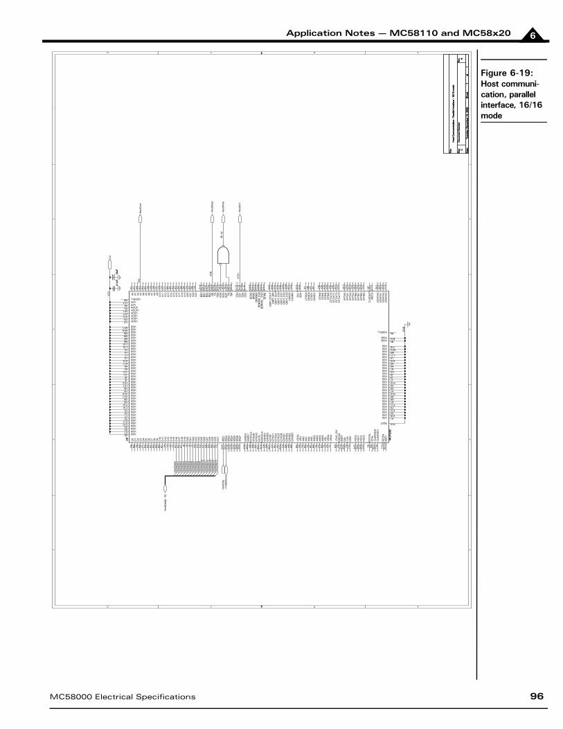
Application Notes — MC58110 and MC58x20 6
Figure 6-19:Host communi-cation, parallel interface, 16/16 mode
5 5
4 4
3 3
2 2
1 1
DD
CC
BB
AA
GN
D
IA3
Hos
tDat
a10
Hos
tDat
a13
Hos
tDat
a9
Hos
tDat
a1H
ostD
ata2
Hos
tDat
a14
Hos
tDat
a11
Hos
tDat
a6
Hos
tDat
a0
Hos
tDat
a5H
ostD
ata4
Hos
tDat
a15
Hos
tDat
a8
Hos
tDat
a3
Hos
tDat
a12
Hos
tDat
a7
~IO
E
IR/~
W
~IC
S1
VCC
Hos
tDat
a[0.
.15]
Hos
tRdy
~Hos
tWrit
e
~Hos
tSlc
t
Hos
tCm
d
~Hos
tRea
d
VCC
~Hos
tInte
rrupt
Title
Size
Doc
umen
t Num
ber
Rev
Dat
e:Sh
eet
of
A
Hos
t Com
mun
icat
ion
- Par
alle
l Int
erfa
ce -
16/1
6 m
ode
C
11
Tues
day,
Dec
embe
r 12,
200
6
Title
Size
Doc
umen
t Num
ber
Rev
Dat
e:Sh
eet
of
A
Hos
t Com
mun
icat
ion
- Par
alle
l Int
erfa
ce -
16/1
6 m
ode
C
11
Tues
day,
Dec
embe
r 12,
200
6
Title
Size
Doc
umen
t Num
ber
Rev
Dat
e:Sh
eet
of
A
Hos
t Com
mun
icat
ion
- Par
alle
l Int
erfa
ce -
16/1
6 m
ode
C
11
Tues
day,
Dec
embe
r 12,
200
6
U8 MC
F528
2
U8 MC
F528
2
D0
P6
D1
R6
D2
T6D
3N
5D
4P
1D
5N
3D
6N
2D
7N
1D
8M
4D
9M
3D
10M
2D
11M
1D
12L4
D13
L3D
14L2
D15
L1D
16K
3D
17K
2D
18K
1D
19J4
D20
J3D
21J2
D22
J1D
23H
4D
24H
3D
25H
2D
26H
1D
27G
4D
28G
3D
29G
2D
30G
1D
31F3
A0
F2A
1F1
A2
E4
A3
E3
A4
E2
A5
E1
A6
D4
A7
D3
A8
D2
A9
D1
A10
C3
A11
C2
A12
C1
A13
B2
A14
B1
A15
A2
A16
A3
A17
B3
A18
A4
A19
B4
A20
C4
A21
A5
A22
B6
A23
C6
VDDE6VDDE7VDDE8VDDE9VDDE10VDDE11
VDDF7VDDF8VDDF9VDDF10VDDF12VDDG5VDDG6VDDG11VDDG12VDDH5VDDH6VDDH11VDDH12VDDJ5VDDJ6VDDJ11VDDJ12VDDK5VDDK6VDDK11VDDK12VDDL5VDDL7VDDL8VDDL9VDDL10VDDL12VDDM6VDDM7VDDM8VDDM9VDDM10VDDM11
VDDFC5
VDDFA12 VDDFD5
VDDFD11VSTBYN11
VPPC11
BS
0R
16B
S1
R15
BS
2T1
5B
S3
P14
OE
N16
TAP
16TE
AP
15R
/WN
15S
IZ0
M16
SIZ
1N
14TS
M15
TIP
M14
CS
0L1
3C
S1
L14
CS
2L1
5C
S3
L16
SC
AS
H16
SR
AS
H15
DR
AM
WG
15S
DR
AM
_CS
0G
16S
DR
AM
__C
S1
H13
SC
KE
H14
IRQ
1D
15IR
Q2
D14
IRQ
3C
16IR
Q4
C15
IRQ
5C
14IR
Q6
B16
IRQ
7B
15
EM
DIO
C10
EM
DC
B10
ETX
CLK
A8
ETX
EN
D6
ETX
DO
D7
EC
OL
B11
ER
XC
LKA
10E
RX
DV
C8
ER
XD
OD
9E
CR
SA
11
ETX
ER
D10
ER
XE
RB
8
ETX
D1
C7
ETX
D2
B7
ETX
D3
A7
ER
XD
1C
9E
RX
D2
B9
ER
XD
3A
9
QS
PI_
DO
UT
F13
QS
PI_
DIN
E16
QS
PI_
CLK
F14
QS
PI_
CS
0F1
5Q
SP
I_C
S1
F16
QS
PI_
CS
2G
13Q
SP
I_C
S3
G14
CA
NTX
E13
CA
NR
XD
16
SC
LE
15S
DA
E14
UTX
D0
T7
UTX
D1
P7
UR
XD
0N
6
UR
XD
1R
7
DTI
N0
J14
DTI
N1
J16
DTI
N2
K14
DTI
N3
K16
DTO
UT0
J13
DTO
UT1
J15
DTO
UT2
K13
DTO
UT3
K15
GP
TA0
N13
GP
TA1
P13
GP
TA2
R13
GP
TA3
T13
GP
TB0
N12
GP
TB1
P12
GP
TB2
R12
GP
TB3
T12
AN
0T3
AN
1R
2A
N2
T2A
N3
R1
AN
52R
4A
N53
T4A
N55
P3
AN
56R
3
VD
DA
R5
VR
HP
4
VR
LT5
VS
SA
P5
JTA
G_E
NR
9D
SC
LKP
9B
KP
TP
10D
SI
R10
TCK
T9
DD
ATA
0B
13D
DA
TA1
A13
DD
ATA
2D
12D
DA
TA3
C12
PS
T0A
15P
ST1
B14
PS
T2A
14P
ST3
C13
VDDPLLN8
RS
TIR
11
RS
TOP
11E
XTA
LT8
CLK
OU
TN
7
CLK
MO
D0
R14
CLK
MO
D1
T14
RC
ON
T11
DS
OT1
0
TEST N10
XTA
LR
8
VSS A1VSS A16
VSS G7VSS G8VSS G9VSS G10VSS H7VSS H8VSS H9VSS H10VSS J7VSS J8VSS J9VSS J10VSS K7VSS K8VSS K9VSS K10VSS L6VSS L11
VSS E5VSS E12VSS F6VSS F11
VSS M5VSS M12VSS T16
VSSPLL P8
VDDHP2
VS
SA
T1
VPPA6
VSSF B5VSSF B12
VDDF5
10uF
10uF
0.1u
F0.
1uF
MC58000 Electrical Specifications 96
Application Notes — MC58110 and MC58x206
6.15.2 8/16 Host Interface
In this example, a PIC microcontroller with limited I/O pins is interfaced with the IO chip. The minimum number of I/O pins required for the parallel 8/16 communications mode is eight bi-directional pins for the data, and five additional pins for the control signals (four outputs and one input). These signals are shown in Figure 6-20.
The PIC16F648 features:
An 8-bit microcontroller core
Up to 10 MHz clock at 3.3V voltage supply
16 I/O pins divided into two ports, with a high impedance state and weak internal pull-up.
The eight I/O pins of the PORTB are used to connect to the IO chip’s HostData bus (pins 0 through 7). The five pins
of the PORTA are reserved for the control signals, as shown in the following table.
Shown below is a typical sequence of events for performing the host read and write cycle.
6.15.2.1 Typical Data / Status Read Sequence
Where:
Step 1: May be performed using the BTFSS instruction. This step must loop until HostRdy is high.
Step 2: Write a byte into PORTA with the lowest four bits set to either 0x4 (data) or 0x6 (status) using the MOVLW and MOVWF instructions.
Step 3: Read Port B and store the result.
Step 4: Write a byte into PORTA with the lowest four bits set to either 0xC or 0xE to deactivate ~HostRead.
Step 5: Repeat steps 2 - 4 for the LSB.
Step 6: Write a byte into PORTA with the lowest four bits set to 0xF to deactivate ~HostSlct.
IO Chip Signal PIC16F648 Signal Dir CommentsHostData0-7 PORTB RB0-RB7 I/O Should be pulled up (Bit 7 of the OPTION register).
Should be kept in high impedance state unless written to.~HostSlct PORTA RA0 OHostCmd PORTA RA1 O~HostWrite PORTA RA2 O~HostRead PORTA RA3 OHostRdy PORTA RA6 I
1 Read HostRdy bit
2Activate~HostSlct = Low ~HostRead = Low
3Read PORTB for MSB
4Deactivate~HostRead = Hi
5 Repeat steps 2-4 for the LSB
6Deactivate~HostSlct = Hi
97 MC58000 Electrical Specifications
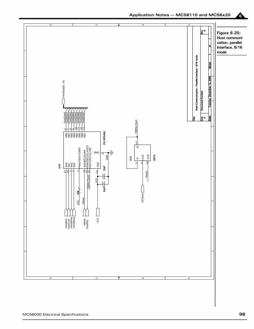
Application Notes — MC58110 and MC58x20 6
Figure 6-20:Host communi-cation, parallel interface, 8/16 mode
5 5
4 4
3 3
2 2
1 1
DD
CC
BB
AA
Hos
tDat
a0H
ostD
ata1
Hos
tDat
a2H
ostD
ata3
Hos
tDat
a4H
ostD
ata5
Hos
tDat
a6H
ostD
ata7
VC
C
~Res
et
10M
Hz
Clo
ck
10M
Hz
Clo
ck
~Res
et
VC
C
GN
D
~Res
et
Hos
tDat
a[0.
.15]
~Hos
tSlc
tH
ostC
md
~Hos
tWrit
e~H
ostR
ead
Hos
tRdy
CP
Clo
ck
VC
C
Title
Siz
eD
ocum
ent N
umbe
rR
ev
Dat
e:S
heet
of
A
Hos
t Com
mun
icat
ion
- Par
alle
l Int
erfa
ce -
8/16
mod
e
A
11
Tues
day,
Dec
embe
r 12,
200
6
Title
Siz
eD
ocum
ent N
umbe
rR
ev
Dat
e:S
heet
of
A
Hos
t Com
mun
icat
ion
- Par
alle
l Int
erfa
ce -
8/16
mod
e
A
11
Tues
day,
Dec
embe
r 12,
200
6
Title
Siz
eD
ocum
ent N
umbe
rR
ev
Dat
e:S
heet
of
A
Hos
t Com
mun
icat
ion
- Par
alle
l Int
erfa
ce -
8/16
mod
e
A
11
Tues
day,
Dec
embe
r 12,
200
6
U12
DFF
2
U12
DFF
2
Q1
D2
CLK
3
CLR
4
+10
uF+
10uF
U10
PIC
16F6
48A
U10
PIC
16F6
48A
GND 5
RA
6/O
SC
2/C
LKO
UT
15
RA
017
RA
118
RA
21
RA
32
RB
06
RB
17
RB
28
RB
39
RB
410
RB
511
RB
612
RB
713
RA
5/M
CLR
/VP
P4
RA
7/O
SC
1/C
LKIN
16
RA
4/T0
CK
1/C
MP
23
VD
D14
10K
10K
10nF
10nF
MC58000 Electrical Specifications 98
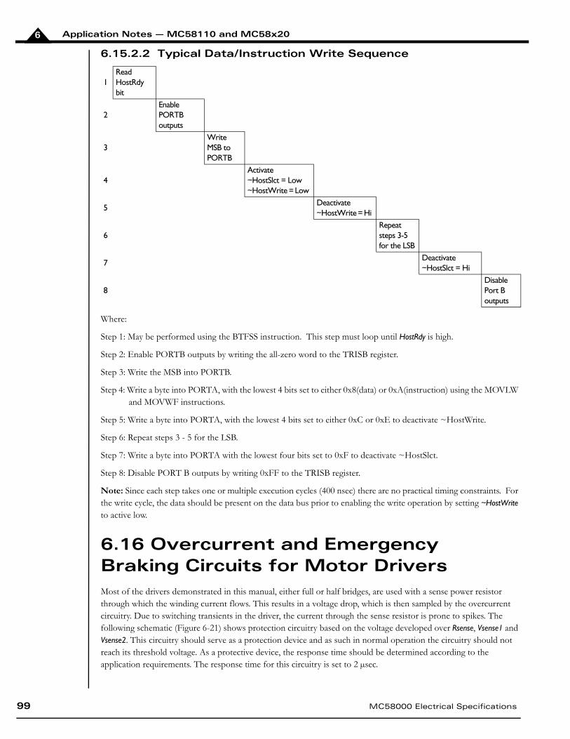
Application Notes — MC58110 and MC58x206
6.15.2.2 Typical Data/Instruction Write Sequence
Where:
Step 1: May be performed using the BTFSS instruction. This step must loop until HostRdy is high.
Step 2: Enable PORTB outputs by writing the all-zero word to the TRISB register.
Step 3: Write the MSB into PORTB.
Step 4: Write a byte into PORTA, with the lowest 4 bits set to either 0x8(data) or 0xA(instruction) using the MOVLW and MOVWF instructions.
Step 5: Write a byte into PORTA, with the lowest 4 bits set to either 0xC or 0xE to deactivate ~HostWrite.
Step 6: Repeat steps 3 - 5 for the LSB.
Step 7: Write a byte into PORTA with the lowest four bits set to 0xF to deactivate ~HostSlct.
Step 8: Disable PORT B outputs by writing 0xFF to the TRISB register.
Note: Since each step takes one or multiple execution cycles (400 nsec) there are no practical timing constraints. For the write cycle, the data should be present on the data bus prior to enabling the write operation by setting ~HostWrite to active low.
6.16 Overcurrent and Emergency Braking Circuits for Motor DriversMost of the drivers demonstrated in this manual, either full or half bridges, are used with a sense power resistor through which the winding current flows. This results in a voltage drop, which is then sampled by the overcurrent circuitry. Due to switching transients in the driver, the current through the sense resistor is prone to spikes. The following schematic (Figure 6-21) shows protection circuitry based on the voltage developed over Rsense, Vsense1 and Vsense2. This circuitry should serve as a protection device and as such in normal operation the circuitry should not reach its threshold voltage. As a protective device, the response time should be determined according to the application requirements. The response time for this circuitry is set to 2 µsec.
1Read HostRdy bit
2Enable PORTB outputs
3Write MSB to PORTB
4Activate~HostSlct = Low ~HostWrite = Low
5Deactivate~HostWrite = Hi
6Repeat steps 3-5 for the LSB
7Deactivate~HostSlct = Hi
8Disable Port B outputs
99 MC58000 Electrical Specifications
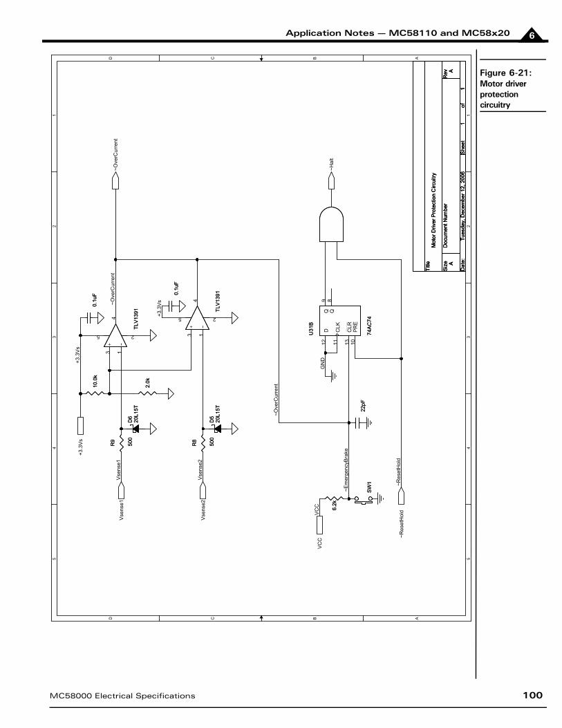
Application Notes — MC58110 and MC58x20 6
Figure 6-21:Motor driver protection circuitry
5 5
4 4
3 3
2 2
1 1
DD
CC
BB
AA
+3.3
Vs
Vse
nse1
Vse
nse2
~Ove
rCur
rent
+3.3
Vs
~Res
etH
old
VC
CG
ND
~Ove
rCur
rent
~Em
erge
ncyB
rake
Vse
nse1
Vse
nse2
+3.3
Vs
VC
C
~Res
etH
old
~Ove
rCur
rent
~Hal
t
Title
Siz
eD
ocum
ent N
umbe
rR
ev
Dat
e:S
heet
of
A
Mot
or D
river
Pro
tect
ion
Circ
uitry
A
11
Tues
day,
Dec
embe
r 12,
200
6
Title
Siz
eD
ocum
ent N
umbe
rR
ev
Dat
e:S
heet
of
A
Mot
or D
river
Pro
tect
ion
Circ
uitry
A
11
Tues
day,
Dec
embe
r 12,
200
6
Title
Siz
eD
ocum
ent N
umbe
rR
ev
Dat
e:S
heet
of
A
Mot
or D
river
Pro
tect
ion
Circ
uitry
A
11
Tues
day,
Dec
embe
r 12,
200
6
22pF
22pF
2.0k
2.0k
0.1u
F0.
1uF
D5
20L1
5TD
520
L15T
U31
B
74A
C74
U31
B
74A
C74
CLR
13
D12
CLK
11
PR
E10
Q9
Q8
6.2k
6.2k
-+
TLV
1391
-+
TLV
1391
3 14
5 2
R8
500
R8
500
R9
500
R9
500
0.1u
F0.
1uF
SW
1S
W1
-+
TLV
1391
-+
TLV
1391
3 14
5 2
D6
20L1
5TD
620
L15T
10.0
k10
.0k
MC58000 Electrical Specifications 100
Application Notes — MC58110 and MC58x206
The comparator is a TLV1391, which is a single supply, fast response, open collector output. The TLV1391 tolerates an input range as low as –0.3V. Because the sense voltage may fall below this range, a protection diode is added, with a VF = 0.25V. In order to avoid false over-current detection, the sense signal is low pass filtered with a cut off
frequency in the MHz region. This is achieved with the use of a 500 resistor and the capacitance of the Schottky diode. The nominal reference voltage of the comparator is set to 0.55V, which is selected to be 80% higher than the nominal voltage drop over Rsense at the rated current of the motor windings (0.3V). The typical response time of the TLV1391 is 800 nsec; leaving ~1 µsec response time for the driver itself. Additional input branches may be added to the ~OverCurrent circuitry. In this case, the value of the pull-up resistor should be re-calculated. The resultant ~OverCurrent signal may either be used for the momentary disabling of the motor’s driver, or to halt it completely until the next ~Reset signal is generated.
An external switch, ~EmergencyBrake, is used as an additional method for halting the motor. Note that the U31B D-FF may momentarily have both Clear and Preset inputs active low.
6.17 DC Brush Motor Control Using SPI Interfaced DACsThe example in Figure 6-22 shows a cost-effective solution for controlling DC brush motors using the SPI interface to an Analog Devices 16-bit DAC AD1866. The AD1866 incorporates 5V CMOS logic with TTL compatible inputs, enabling a direct interface to the 3.3V MC58000 outputs. In all respects the SPI interface requirements of the AD1866 impose no practical limitations. The Magellan SPI port can be configured using the SetSPIMode command to either falling edge without phase delay, or rising edge with phase delay, in order to maintain compatibility with the AD1866 SPI port. The AD1866 requires twos-complement data format which can be selected with the Magellan SetOutputMode command.
Note that only SPI DACs which support 16-bit packets can be used.
6.17.1 Conditioning CircuitryThe AD1866 analog output, Vo, is a 1Vpp output, V, centered at the Vref = 2.5V reference voltage; in other words, Vo = Vref + V. The AD1866 has moderate accuracy, with a mid-scale error of 30 mV at 3% of the full range, and a gain error of 3% of the full range. The goals of the conditioning circuitry are to amplify the output to the 10V range, and to provide a means to disable the AD1866 outputs until the MC58000 generates the first valid DAC word.
There are two methods for interfacing the AD1866 to a motor amplifier. First, when the output voltage is referenced to Vref, and the second is when it is referenced to the signal ground. The first solution is simpler, since it doesn’t involve high precision matching resistors, but the appropriate method for a given application will depend on the requirements of the motor amplifier. Note that both interfaces use single-ended transmission. If the system requires differential transmission, then changes to the design will be required.
6.17.2 Referencing to VrefAn operational amplifier (U6) and two resistors (R1 and R2), are used to generate a 10V differential output (VDAC),
which is referenced to Vref.
VDAC = V (R2/R1) + Vref (1)
Selecting R2 = 100 k (%1) and R1 = 10.0 k (%1) results in an amplification gain of AM = 10.
In order to avoid starting the motors in an unknown state at power-up, the DAC’s output voltage is wired through a buffer equipped with shut-down capability. At power-up or reset, this buffer will be in shutdown mode resulting in high impedance output. In this state, the inverting x10 amplifier output will be Vref. Vref is wired through a buffer, since it is not designed to sink or source the large currents that may be required at the input stage of the motor amplifier.
Since the DAC performance poses no practical requirements on the op-amp selection, the selected components are the TLE2021, and dual TLV2473 with shutdown. The TLE2021 is capable of swinging up to the required worst-case +12.5+(0.6)V, but has a relatively large bias current. R3 = R1||R2 is used in order to reduce the effect of the bias current.
101 MC58000 Electrical Specifications
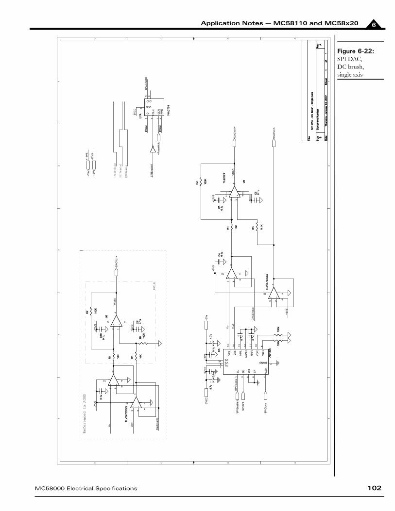
Application Notes — MC58110 and MC58x20 6
Figure 6-22:SPI DAC, DC brush, single axis
5 5
4 4
3 3
2 2
1 1
DD
CC
BB
AA
SP
IEna
ble
Vre
f
+5V
S
Vo
+15V
S
-15V
S
SP
IEna
ble1
DA
CE
nabl
e
Dac
Ena
ble
Vre
f
+15V
S
-15V
S
VD
AC
DA
CE
nabl
e
Vo
+5V
S
+5V
S
+5V
S
VD
AC
5VC
C
+15V
S
-15V
S
5VC
C5V
CC
5VC
C5V
CC
5VC
C
~Res
etH
old
5VC
C+5
Vs
DA
CV
o1+
DA
CV
o1+
DA
CV
o1-
SP
IXm
t
SP
IClo
ck
SP
IEna
ble1
+15V
s
-15V
s
Title
Siz
eD
ocum
ent N
umbe
rR
ev
Dat
e:S
heet
of
A
SP
I DA
C -
DC
Bru
sh -
Sin
gle
Axi
s
B
11
Thur
sday
, Jan
uary
04,
200
7
Title
Siz
eD
ocum
ent N
umbe
rR
ev
Dat
e:S
heet
of
A
SP
I DA
C -
DC
Bru
sh -
Sin
gle
Axi
s
B
11
Thur
sday
, Jan
uary
04,
200
7
Title
Siz
eD
ocum
ent N
umbe
rR
ev
Dat
e:S
heet
of
A
SP
I DA
C -
DC
Bru
sh -
Sin
gle
Axi
s
B
11
Thur
sday
, Jan
uary
04,
200
7
Referenced to AGND
INA143
SPIEnable1
DACEnable
~ResetHold
C10
0.1uC
100.
1u
- +
U6
- +
U6
1
2
34
5
-+
TLV
2473
DQ
G -+
TLV
2473
DQ
G
4
13 2
10
5
R3
10K
R3
10K
-+
TLV
2473
DQ
G
-+
TLV
2473
DQ
G
4
13 2
10
50.
1u0.
1u
R3
9.1K
R3
9.1K
C5
0.1uC5
0.1u
0.1u
0.1u
+4.
7u+
4.7u
100k
100k
- +
U6
TLE
2021
- +
U6
TLE
2021
326
71
45
U7A 74
AC
T74
U7A 74
AC
T74
D2
CLK
3
Q5
Q6
VCC14
PR
E4
CLR
1
R1
10K
R1
10K
100k
100k
0.1u
0.1u
+
4.7u
+
4.7u
C4
0.1u
C4
0.1u
C11
0.1u
C11
0.1u
R1
10K
R1
10K
U3
AD
1866U3
AD
1866
LL2
DL
3
DR
5
LR6
VL1
VS15 DGND 7
AG
ND
12
VS9
CLK
4
VB
L16
VO
L14
NR
L13
NR
R11
VO
R10
VB
R8
+
4.7u
+
4.7uR
410
0KR
410
0K
C6
0.1u
C6
0.1u
-+ -+
4
97 8
10
6
-+ -+
4
97 8
10
6
R2
100K
R2
100K
R2
100K
R2
100K
+4.
7u+
4.7u
MC58000 Electrical Specifications 102

Application Notes — MC58110 and MC58x206
6.17.3 Referencing to AGND
By adding an additional resistor, R4, and selecting R2 = R4 = 100 k (1%), and R1 = R3 = 10.0 k (1%), U6 becomes
a differential amplifier with a nominal gain of 10.
VDAC = - V R2/R1 (2)
This equation only holds true for matching pairs of resistors; otherwise undesired biases will not be completely canceled out, resulting in common-mode voltage. Using a 1% tolerant resistor will result in ~1% bias in the output signal. This bias is only one third of the AD1866 tolerances, but it should not be ignored. If this accuracy is not adequate, then high precision 0.1% resistors may be used. Alternately, the entire resistor set and amplifier may be replaced by a differential amplifier, such as the INA106 or the INA143, which offer a fixed gain of 10 and high CMRR.
A dual TLV2473 is used in order to ground the output at reset or power-up. The resulting circuitry forms an instrumental amplifier, which also benefits from the small output impedance of the buffers; thus minimizing the CMRR even further.
Notes:
1 In the dual-chip configuration (MC58x20), when more than one motor is to be driven by the SPI DAC,use the SPIEnable1-4 signals (which are sourced by the IO chip) as chip-selects to enable the appropriateSPI port. For instance, if the right port of the AD1866 is to be used to drive a second motor connectSPIEnable2 and SPIXmt to the AD1866’s LR and DR input pins, respectively.
2 In both conditioning circuitries, an inverting amplifier (U6) is used. This may require that the motoroutput signal be inverted by setting bit 12 in the Magellan signal sense register.
3 The DACEnable signal goes active high on the first write to the DACs after the ~ResetHold active low periodhas completed. Note that if the AD1866 is used to drive two motors, then the DACEnable signal shouldbe generated with the use of the SPIEnable signal that corresponds to the last of the two motors beingwritten to.
4 The AD1866 analog signal power supply should be decoupled with capacitors placed as closely aspossible to both the supply pins and the signal ground. Refer to the AD1866 data sheet for a completedescription.
5 The TLV2473 shutdown input accepts TTL input levels, which can be fed by a 3.3V CMOS D-FF (U7).If other op-amps are selected, then the shutdown input levels should be checked. If there is levelincompatibility the D-FF may be selected from the HCT/ACT family.
103 MC58000 Electrical Specifications

Application Notes — MC58110 and MC58x20 6
6.18 Brushless DC Motor Control Using High-Precision Parallel DACsIn this example, TI’s high accuracy 16-bit parallel DAC7744 is used to drive four brushless DC motors. The MC58420 uses the peripheral address space to access the correct driver, with the Addr14 signal used as a chip-select, as detailed
in the following table.
The DAC7744 is a four channel, digital-to-analog converter (DAC). The four channels are divided into two pairs; each fed by a different reference voltage. In order to minimize the effects of the mismatches, the DAC7744 pair of channels (which share the same reference) are used for driving Phase A and Phase B of the same motor.
The schematic in Figure 6-23 indicates that two DAC7744 components are required. The Addr2 signal is used to select between the two devices, and the Addr0 and Addr1 lines are used to write into the appropriate channel’s input buffer register. As the order of writes from the CP is Phase B followed by Phase A, the LSB of the address is used to generate the LDDACS signal, which is used by the DAC7744 to latch the input buffer registers. In this manner, the new values for both phases take effect simultaneously. The DAC7744 supports 5V CMOS input voltages. To interface it with the MC58000 data bus, a transparent latch with TTL input voltage compatibility, the 74ACT373, and its 10-bit version 74ACT841, are used. The propagation delay of these latches is less than 11 nsec. All other logic interfacing to the DAC7744 has TTL compatible inputs, and is supplied with +5V.
The digital input stage of the DAC7744 imposes several stringent timing requirements. To meet these requirements, the ~WriteEnable signal is sampled on the rising edge of ClockOut, and a ~CS pulse of 75 nsec is generated out of it. In order for the data to be ready at least 40 µsec before the rising edge of ~CS, the propagation delay through the 5V data buffers should be less than 15 µsec. This requirement is satisfied by the 74ACT373 and 74ACT841. In order to satisfy the 15 µsec hold time, the propagation delay through the D-FF and its subsequent logic should be less than 20 µsec. Assuming 10 µsec for the 74AHCT32 OR gates leaves 10 µsec for the D-FF, which is sufficient for the 74LVT74. Note that the U6 OR gate should have a propagation delay of less than 6.5 µsec, minus the setup time of the D-FF (1.7 µsec for 74LVT74). Since LDDACS only goes active once per axis, the DAC’s requirements for a period of at least 80 µsec between the rising edge of the LDDACS signal and the next falling edge of ~CS is met.
At power-up or reset, the ~CS signals will be held inactive high while the MC58000 completes its initialization which occurs during the ~ResetHold active low period. During this time undesired values will not latch into the DACs.
6.18.1 Analog SignalsThe schematic in Figure 6-24 demonstrates a high-precision DAC solution. In order to maintain the accuracy of the DAC, it should be supplied with high accuracy reference voltages with tolerances of less than half the LSB. The AD2702 or AD688 voltage regulators may be used (see Figure 6-1).
For improved accuracy, the DAC7744 is equipped with sensing mechanisms on both the reference voltages and the analog output signals. These allow for compensation of the board’s wiring resistances. The AD688, which is used to generate the 10V reference voltage, provides sensing pins. These pins may be tied to the reference sensing inputs in the DAC7744 to compensate for the resistance path. The AD688 may source/sink 10 mA of current on each of the output pins, and should be able to drive up to two dual DAC7744 components. The AD688 provides calibration pins, which may be used to reduce the initial 2 mV error as described in the AD688 data sheet. The 2 mV error will translate to 8 LSB accuracy for the 16-bit DAC. Achieving full 16-bit resolution implies that the error budget and noise levels should be kept below 150 µV. If such precision is not required, less accurate components from the same family may be used, such as the DAC7744E.
Address 4000h 4001h 4002h 4003h 4004h 4005h 4006h 4007hOutput Axis1A Axis1B Axis2A Axis2B Axis3A Axis3B Axis4A Axis4B
MC58000 Electrical Specifications 104
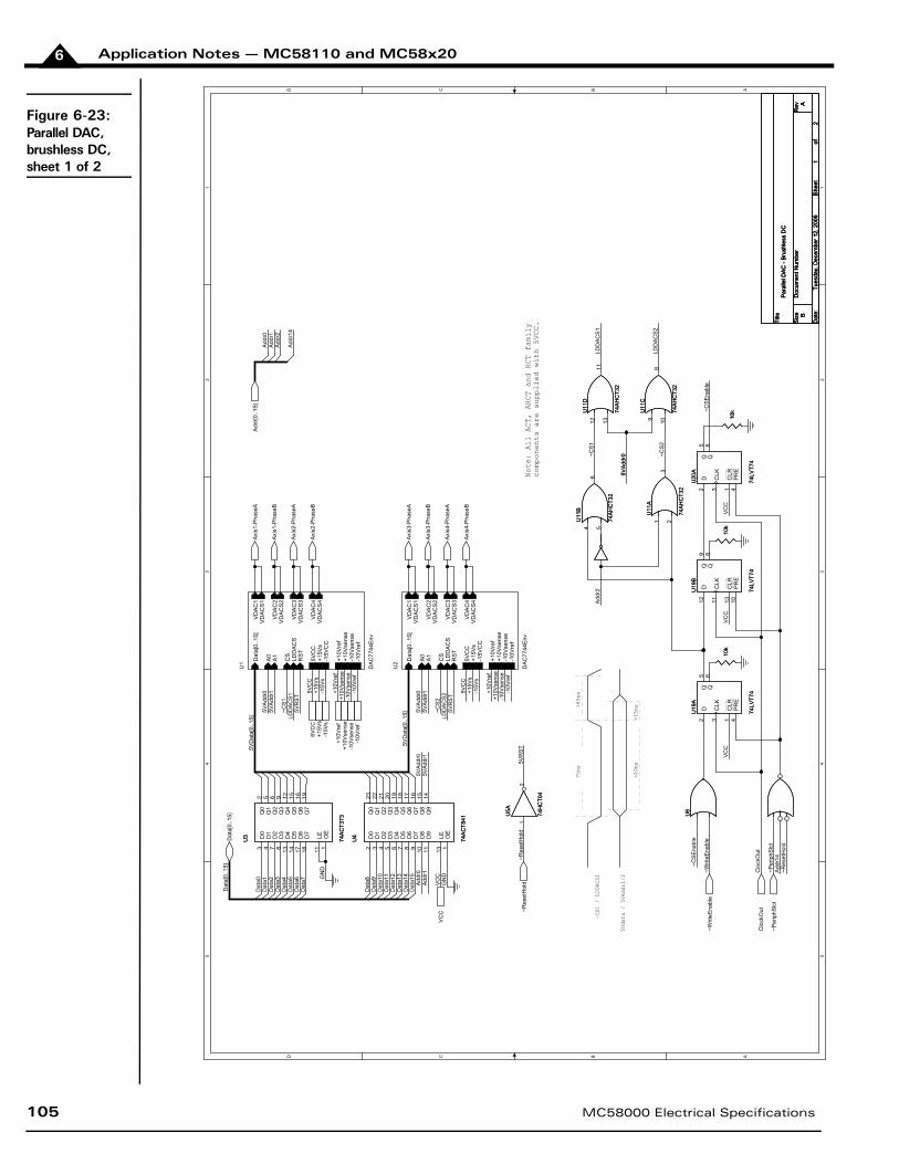
Application Notes — MC58110 and MC58x206
Figure 6-23:Parallel DAC, brushless DC, sheet 1 of 2
5 5
4 4
3 3
2 2
1 1
DD
CC
BB
AA
5VD
ata[
0..1
5]
GN
D
GN
D
Dat
a0D
ata1
Dat
a2D
ata3
Dat
a4D
ata5
Dat
a6D
ata7
Dat
a8D
ata9
Dat
a10
Dat
a11
Dat
a12
Dat
a13
Dat
a14
Dat
a15
Dat
a[0.
.15]
5VA
ddr0
5VA
ddr1
5VR
ST
5VD
ata[
0..1
5] 5VA
ddr0
5VA
ddr1
5VR
ST
5VR
ST
Add
r0A
ddr1
5VA
ddr0
5VA
ddr1
~CS
2
~CS
1
LDD
AC
S2
~Res
etH
old
VC
C
Clo
ckO
ut
Add
r14
~Per
iphS
lct
~Writ
eEna
ble
~CS
2
~CS
Ena
ble
~Res
etH
old
VC
C
~CS
Ena
ble
VC
C
VC
C
LDD
AC
S1
~CS
1
5VA
ddr0
5VA
ddr0
LDD
AC
S2
LDD
AC
S1
Add
r0A
ddr1
Add
r2
Add
r14
Add
r2
5VC
C+1
5Vs
-15V
s
+10V
sens
e-1
0Vse
nse
+10V
ref
-10V
ref
+15V
s-1
5Vs
+10V
sens
e-1
0Vse
nse
+10V
ref
-10V
ref
5VC
C
~Res
etH
old
Axi
s1-P
hase
A
Axi
s1-P
hase
B
Axi
s2-P
hase
A
Axi
s2-P
hase
B
Axi
s3-P
hase
B
Axi
s4-P
hase
A
Axi
s4-P
hase
B
Axi
s3-P
hase
A
Dat
a[0.
.15]
VC
C
~Writ
eEna
ble
Clo
ckO
ut
~Per
iphS
lct
Add
r[0..1
5]
5VC
C+1
5Vs
-15V
s
-10V
sens
e
+10V
ref
+10V
sens
e
-10V
ref
Title
Siz
eD
ocum
ent N
umbe
rR
ev
Dat
e:S
heet
of
A
Par
alle
l DA
C -
Bru
shle
ss D
C
B
12
Tues
day,
Dec
embe
r 12,
200
6
Title
Siz
eD
ocum
ent N
umbe
rR
ev
Dat
e:S
heet
of
A
Par
alle
l DA
C -
Bru
shle
ss D
C
B
12
Tues
day,
Dec
embe
r 12,
200
6
Title
Siz
eD
ocum
ent N
umbe
rR
ev
Dat
e:S
heet
of
A
Par
alle
l DA
C -
Bru
shle
ss D
C
B
12
Tues
day,
Dec
embe
r 12,
200
6
~CS1 / LDDACS1
5Vdata / 5VAddr1/2
75ns
>40ns
>80ns
>15ns
Note: All ACT, AHCT and HCT family
components are supplied with 5VCC.
U20
A
74LV
T74
U20
A
74LV
T74
CLR
1
D2
CLK
3
PR
E4
Q5
Q6
10k
10k
10k
10k
10k
10k
U19
B
74LV
T74
U19
B
74LV
T74
CLR
13
D12
CLK
11
PR
E10
Q9
Q8
U4
74A
CT8
41
U4
74A
CT8
41
D0
2D
13
D2
4D
35
D4
6D
57
D6
8D
79
D8
10D
911
LE13
OE
1
Q0
23Q
122
Q2
21Q
320
Q4
19Q
518
Q6
17Q
716
Q8
15Q
914
U2
DA
C77
44E
nv
Dat
a[0.
.15]
A0
A1
CS
RS
TLD
DA
CS
VD
AC
1
VD
AC
2
VD
AC
3
VD
AC
4
VD
AC
S1
VD
AC
S2
VD
AC
S3
VD
AC
S4
5VC
C+1
5Vs
-15V
CC
+10V
ref
+10V
sens
e-1
0Vse
nse
-10V
ref
U11
C
74A
HC
T32
U11
C
74A
HC
T32
9 108
U3
74A
CT3
73
U3
74A
CT3
73
D0
3D
14
D2
7D
38
D4
13D
514
D6
17D
718
OE
1LE
11
Q0
2Q
15
Q2
6Q
39
Q4
12Q
515
Q6
16Q
719
U19
A
74LV
T74
U19
A
74LV
T74
CLR
1
D2
CLK
3
PR
E4
Q5
Q6
U11
B
74A
HC
T32
U11
B
74A
HC
T32
4 56
U11
D
74A
HC
T32
U11
D
74A
HC
T32
12 1311
U5A
74H
CT0
4
U5A
74H
CT0
4
12
U11
A
74A
HC
T32
U11
A
74A
HC
T32
1 23
U1
DA
C77
44E
nv
Dat
a[0.
.15]
A0
A1
CS
RS
TLD
DA
CS
VD
AC
1
VD
AC
2
VD
AC
3
VD
AC
4
VD
AC
S1
VD
AC
S2
VD
AC
S3
VD
AC
S4
5VC
C+1
5Vs
-15V
CC
+10V
ref
+10V
sens
e-1
0Vse
nse
-10V
ref
U6
U6
105 MC58000 Electrical Specifications
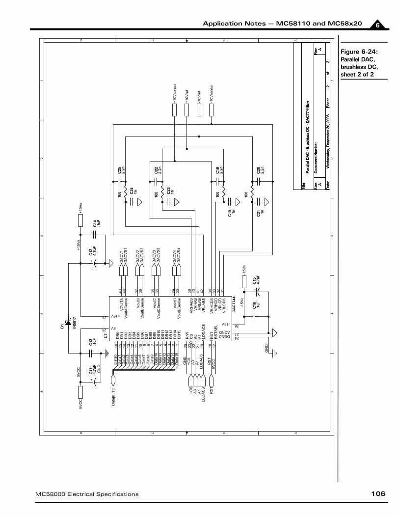
Application Notes — MC58110 and MC58x20 6
Figure 6-24:Parallel DAC, brushless DC, sheet 2 of 2
5 5
4 4
3 3
2 2
1 1
DD
CC
BB
AA
+15V
s
GN
D
Dat
a0D
ata1
Dat
a2D
ata3
Dat
a5D
ata6
Dat
a4
Dat
a7
Dat
a10
Dat
a11
Dat
a9D
ata8
Dat
a15
Dat
a12
Dat
a13
Dat
a14
GN
D~C
SA
0A
1
RS
T5V
CC
LDD
AC
S
GN
D
5VC
C
-15V
s
DA
CV
1D
AC
VS
1
DA
CV
2D
AC
VS
2
DA
CV
3D
AC
VS
3
DA
CV
4D
AC
VS
4
~CS
A0
A1
LDD
AC
S
RS
T
Dat
a[0.
.15]
+15V
s
-15V
s
-10V
ref
-10V
sens
e
+10V
sens
e
+10V
ref
5VC
C
Title
Siz
eD
ocum
ent N
umbe
rR
ev
Dat
e:S
heet
of
A
Par
alle
l DA
C -
Bru
shle
ss D
C -
DA
C77
44E
nv
A
22
Wed
nesd
ay, D
ecem
ber 2
0, 2
006
Title
Siz
eD
ocum
ent N
umbe
rR
ev
Dat
e:S
heet
of
A
Par
alle
l DA
C -
Bru
shle
ss D
C -
DA
C77
44E
nv
A
22
Wed
nesd
ay, D
ecem
ber 2
0, 2
006
Title
Siz
eD
ocum
ent N
umbe
rR
ev
Dat
e:S
heet
of
A
Par
alle
l DA
C -
Bru
shle
ss D
C -
DA
C77
44E
nv
A
22
Wed
nesd
ay, D
ecem
ber 2
0, 2
006
100
100
C13
.1uF
C13
.1uF
C18
2.2n
C18
2.2n
C22
2.2n
C22
2.2n
C23
1nC23
1n
C20
2.2n
C20
2.2n
C16
.1uF
C16
.1uF
100
100 C
241nC
241n
100
100
+C
124.
7uF
+C
124.
7uF
C25
2.2n
C25
2.2n
100
100
D1
IN58
17
D1
IN58
17
C19 1n
C19 1n
C21 1n
C21 1n
C14
.1uF
C14
.1uF
+C
154.
7uF
+C
154.
7uF
U2
DA
C77
44
U2
DA
C77
44
DB
016
DB
115
DB
214
DB
313
DB
412
DB
511
DB
610
DB
79
DB
88
DB
97
DB
106
DB
115
DB
124
DB
133
DB
142
DB
151
R/W
20C
S23
A0
22A
121
LDD
AC
S19
RS
T18
RS
TSE
L17
VO
UTA
43V
outA
Sen
se44
Vou
tBS
ense
38
Vou
tCS
ense
36
Vou
tDS
ense
30V
outD
29
Vou
tC35
Vou
tB37
VR
HA
BS
39V
RH
AB
40V
RLA
B41
VR
LAB
S42
VR
LCD
S31
VR
LCD
32V
RH
CD
33V
RH
CD
S34
5V25
+15V26
DGND 24AGND 27
-15V 28
+C
114.
7uF
+C
114.
7uF
MC58000 Electrical Specifications 106
Application Notes — MC58110 and MC58x206
6.19 Single-Axis Magellan with Brushless DC AtlasThe following schematic shows a Brushless DC Atlas Amplifier connected to a single-axis Magellan.
6.19.1 Atlas Power Input and Motor OutputAtlas is powered through pin pairs HV and Pwr_Gnd, and the power source is a transformer-isolated DC power supply. When unregulated DC power supply is used the output voltage with respect to its output power/current should meet the full Atlas operating range specification. The power supply should be able to “absorb” the recovered energy when Atlas is in regeneration mode. If a regulated DC power supply is used, but it cannot dump the regenerated energy, a blocking diode between the power supply and HV can be used.
The Pwr_Gnd and GND pins are shorted inside the Atlas, and at a system level they refer to the same ground. Pwr_Gnd, the current return path for the power train, is paired with HV and may therefore be noisy. GND is the reference for the SPI signals and other digital control signals. These signals require a quiet ground reference. To ensure optimal performance, star grounding is recommended for component placement and layout. That is, Pwr_Gnd and GND should be connected to the system ground very close to Atlas, and the two ground paths should be kept away from each other.
There is a third current return path stemming from the high frequency component of the motor winding current. Atlas drives motor windings with pulse-width modulated (PWM) signals. Although the sum of the average winding currents is zero, the high frequency PWM signal may couple to the ground plane and induce noise into other circuits. Therefore, depending on your application, you may consider utilizing a motor shield cable to provide a current return path. If utilized, its ground point should be very close to, or the same, as Pwr_Gnd.
For Brushless DC motors pins MotorA, MotorB and MotorC are wired to motor windings A, B, C, respectively. Pins MotorD are left un-connected.
6.19.2 Atlas SPI Interface
Atlas receives control commands through an SPI interface and functions as an SPI slave. Atlas SPI communication is enabled when ~SPICS is pulled down.
To ensure optimal SPI communication, please consider the following layout recommendations:
1 Keep traces short and use 45 degree corners instead of 90 degree corners.
2 All SPI signal traces should be located next to a continuous ground plane, or if possible, between twocontinuous ground planes.
3 Keep traces away from other noisy and high speed signal traces. Alternatively, run ground traces alongwith these signals as a shield.
4 When multiple Atlas modules are used, keep the SPI signal stubs short.
Note that the Atlas Development Kit layout can be used as a layout reference.
6.19.3 Atlas ~Enable and FaultOut SignalsAtlas has one dedicated input signal, ~Enable, which must be pulled low for the Atlas output stage to be active.
FaultOut is a dedicated output. During normal operation it outputs low. When a fault occurs it will go into a high impedance state. In this example, FaultOut is pulled up by Vpullup through resistor R1. Vpullup can be up to 24V to meet the system requirement. For example, if the fault signal is wired to a 5V TTL input, Vpullup can be 5V.
107 MC58000 Electrical Specifications

Application Notes — MC58110 and MC58x20 6
6.19.4 Magellan MC58110 Configuration
In this schematic the SPI master is a single axis Magellan MC58110. Only the connections with Atlas are shown. For complete Magellan wiring, please refer to the MC58110 electrical specifications.
The MC58110 is configured to default to Atlas motor output by tying pin 7, OutputMode0, to ground. The MC58110 inputs encoder signals, implements motion control and commutation functions, and sends torque commands to Atlas through the SPI interface. Depending on the Magellan commutation method selected the feedback signals HallA, HallB, HallC and ~Index are optional.
MC58000 Electrical Specifications 108
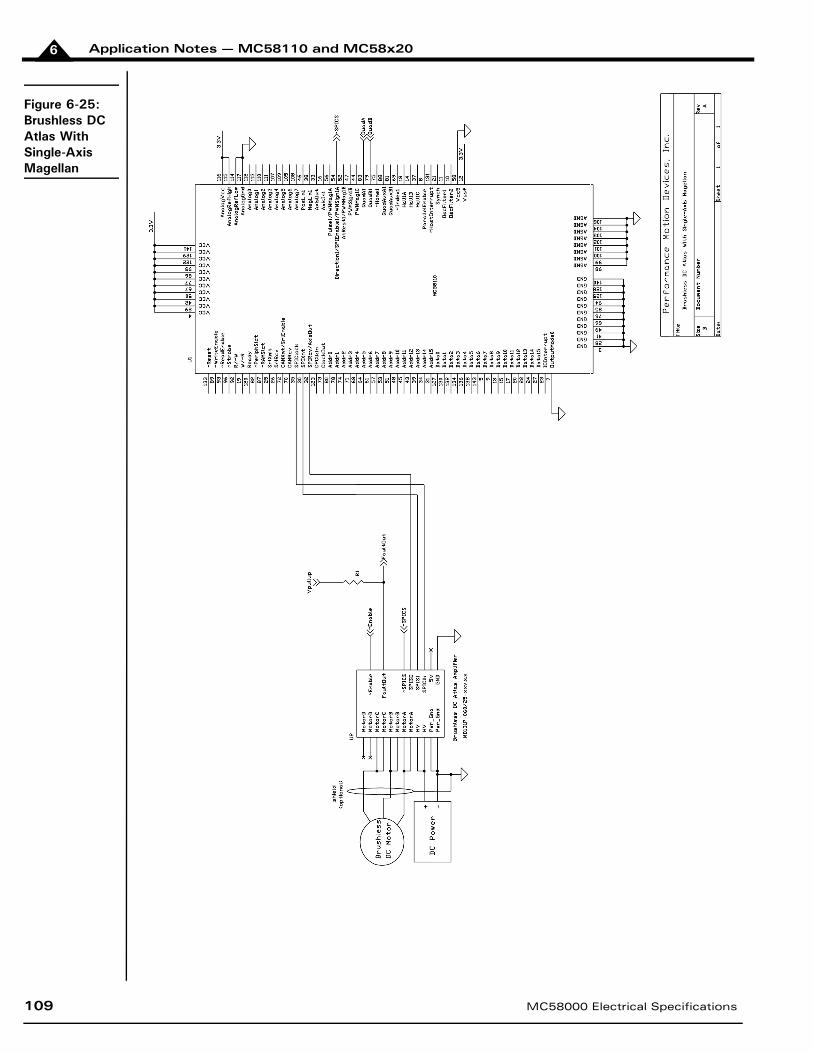
Application Notes — MC58110 and MC58x206
Figure 6-25:Brushless DC Atlas With Single-Axis Magellan
109 MC58000 Electrical Specifications

Application Notes — MC58110 and MC58x20
MC58000 Electrical Specifications 110
6
6.20 Multi-Axis Magellan with DC Brush & Step Motor AtlasThe following schematic shows a two-axis application with one DC Brush Atlas Amplifier and one step motor Atlas amplifier controlled by a multi-axis Magellan.
6.20.1 Atlas Power Input and Motor Output
Atlas is powered through pin pairs HV and Pwr_Gnd, and the power source is a transformer-isolated DC power supply. In this application the two Atlases share the same power supply. Alternatively they could be powered independently so that different motor voltages could be used.
For DC Brush motors pins MotorA and MotorB are wired to motor windings Motor+ and Motor-, respectively. Pins MotorC and MotorD are left un-connected.
For step motors pins MotorA, MotorB, MotorC and MotorD are wired to motor windings A+, A-, B+ and B-, respectively.
Please refer to Section 6.19.1, “Atlas Power Input and Motor Output” for layout and wiring recommendations on power input and motor outputs.
6.20.2 Atlas SPI InterfaceAtlas receives control commands through an SPI interface and functions as an SPI slave. Atlas SPI communication is enabled when ~SPICS is pulled down. Only one Atlas can be enabled at any given time.
Please refer to Section 6.19.1, “Atlas Power Input and Motor Output” for layout recommendation on SPI interface.
6.20.3 Atlas ~Enable and FaultOut SignalsAtlas has one dedicated input signal, ~Enable, which must be pulled low for the Atlas output stage to be active.
FaultOut is a dedicated output. During normal operation it outputs low. When a fault occurs it will go into a high impedance state. In this example, FaultOut is pulled up by Vpullup through resistor R1. Vpullup can be up to 24V to meet the system requirement. Each Atlas may use a different Vpullup voltage, for example, if the fault signal is wired to a 5V TTL input, Vpullup can be 5V.
6.20.4 Magellan MC58420 Configuration
In this schematic the SPI master is a four-axis Magellan MC58420. Only the connections with Atlas are shown. For complete Magellan wiring, please refer to the MC58420 electrical specifications.
The MC58420 is configured to default to Atlas motor output by tying pin 7, OutputMode0, to ground. In this example axis 2 and axis 3 are under control. The MC58420 sends torque commands to the DC Brush Atlas by pulling SPIEnable2 low, and sends position commands to the step motor Atlas by pulling SPIEnable3 low.
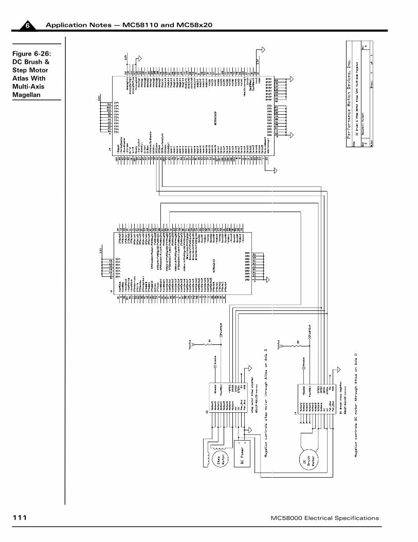
Application Notes — MC58110 and MC58x206
Figure 6-26:DC Brush & Step Motor Atlas With Multi-Axis Magellan
111 MC58000 Electrical Specifications
Application Notes — MC58110 and MC58x20
MC58000 Electrical Specifications 112
6
6.21 Pulse & Direction Mode Output Connected to AtlasThe following schematic shows Atlas operated in pulse & direction mode controlled by a single axis Magellan. Note that any source of pulse & direction signals, such as a microprocessor or other dedicated motion control IC, may be substituted for the Magellan in this schematic.
6.21.1 Atlas power input and motor outputsAtlas is powered through pin pairs HV and Pwr_Gnd, and the power source is a transformer-isolated DC power supply.
For step motors pins MotorA, MotorB, MotorC and MotorD are wired to motor windings A+, A-, B+ and B-, respectively.
Please refer to Section 6.19.1, “Atlas Power Input and Motor Output” for layout and wiring recommendations on power input and motor outputs.
6.21.2 Atlas Pulse & Direction Interface
When in pulse & direction signal mode, Atlas receives pulse, direction and AtRest signals as shown in the schematic. When operated in pulse & direction signal mode SPI communications are not available.
6.21.3 Atlas ~Enable and FaultOut SignalsAtlas has one dedicated input signal, ~Enable, which must be pulled low for the Atlas output stage to be active.
FaultOut is a dedicated output. During normal operation it outputs low. When a fault occurs it will go into a high impedance state. In this example, FaultOut is pulled up by Vpullup through resistor R1. Vpullup can be up to 24V to meet the system requirement. For example, if the fault signal is wired to a 5V TTL input, Vpullup can be 5V.
6.21.4 Magellan MC58110 configurationIn this schematic the SPI master is a single-axis Magellan MC58110 configured for pulse & direction signal output. Only the connections with Atlas are shown. For complete Magellan wiring, please refer to the MC581100 electrical specifications.
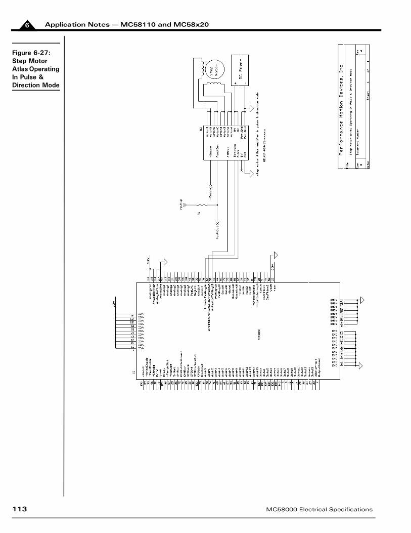
Application Notes — MC58110 and MC58x206
Figure 6-27:Step Motor Atlas Operating In Pulse & Direction Mode
113 MC58000 Electrical Specifications

Application Notes — MC58110 and MC58x20 6
6.22 Using PWM for DC Brush, Brushless DC and Microstepping MotorsThe MC58000 series can drive DC brush and brushless DC motors, with the use of the PWM signals. The PWM magnitude is a symmetric, 10-bit resolution, 19.531 kHz signal. The supplies for the different motor drivers are not shown in the schematics, and it is assumed that the ground is isolated in order to prevent interference from low-signal components.
6.22.1 Using the ST L6234 to Drive Three-Phase Brushless DC Motors
In the following schematic (Figure 6-28), PWM 50/50 outputs are used to drive an L6234 three-phase motor driver. The TTL/CMOS input levels of the L6234 digital part are compatible with the outputs of the MC58000. If the power supply cannot sink the switching currents from the motor, a large capacitor should be added between the Vs input pin and ground. The schematic shows a 47 µF capacitor for a nominal 2A motor.
To detect malfunctions, the Vsense signal may be used to sense the amount of current flowing through the motor windings. For a nominal 2A driving current, an Rsense = 0.15 power resistor may be used to generate the halt signal required by the protection circuitry in Section 6.16, “Overcurrent and Emergency Braking Circuits for Motor Drivers.” Only half of the ~OverCurrent circuitry is required. The halt signal shorts the motor winding to ground. Other braking configurations may be implemented by altering the halt signal interface.
The schematic as shown can be duplicated for multi-axis control.
MC58000 Electrical Specifications 114

Application Notes — MC58110 and MC58x206
Figure 6-28:PWM, brushless DC, L6234
5 5
4 4
3 3
2 2
1 1
DD
CC
BB
AA
Vs=
24V
PW
MM
ag1A
PW
MM
ag1B
PW
MM
ag1C
~Hal
tV
sens
e1
Title
Siz
eD
ocum
ent N
umbe
rR
ev
Dat
e:S
heet
of
A
PW
M -
Bru
shle
ss D
C -
L623
4 - S
ingl
e A
xis
A
11
Tues
day,
Dec
embe
r 12,
200
6
Title
Siz
eD
ocum
ent N
umbe
rR
ev
Dat
e:S
heet
of
A
PW
M -
Bru
shle
ss D
C -
L623
4 - S
ingl
e A
xis
A
11
Tues
day,
Dec
embe
r 12,
200
6
Title
Siz
eD
ocum
ent N
umbe
rR
ev
Dat
e:S
heet
of
A
PW
M -
Bru
shle
ss D
C -
L623
4 - S
ingl
e A
xis
A
11
Tues
day,
Dec
embe
r 12,
200
6
D2
1N41
48
D2
1N41
48+
C1
100u
F+
C1
100u
F
1uF
1uF
U1
L623
4/S
OU1
L623
4/S
OEN
18
OU
T315
SE
NS
E2
19S
EN
SE
12
Vre
f16
Vbo
ot18
Vcp
17
EN
313
EN
23
IN1
7IN
24
IN3
14O
UT1
6O
UT2
5
Vs9
GND 10Vs12 GND 11GND 1GND 20
Rse
nse1
Rse
nse1
0.1u
F0.
1uF
220n
F22
0nF
10nF
10nF
D1
1N41
48
D1
1N41
48
115 MC58000 Electrical Specifications
Application Notes — MC58110 and MC58x20 6
6.22.2 Using the National LMD18200 to Drive DC Brush Motors
In the following schematic (Figure 6-29), a magnitude and direction PWM signal is used to drive a DC brush motor with a nominal 24V, 2A drive. The H-bridge driver selected for this task is the LMD18200, which can be driven directly from a 3.3V CMOS logic output and as such can be directly interfaced to the MC58000.
There are two methods in which the output current of the H-bridge may be controlled.
First, in the locked anti-phase control mode (see the LMD18200 data sheet), a 50/50 PWM signal is applied to the LMD18200 DIR input, while the PWM input is tied high. The current ripple in this mode is relatively high, as the circulating currents are quickly decaying.
Second, in the sign/magnitude control mode, sign and magnitude PWM signals are applied to both the PWM and DIR inputs of the LMD18200. In this mode, the resultant current ripple is reduced resulting in smoother operation of the motor. When the acceleration/deceleration requirements for the motor are not high, the sign/magnitude PWM control mode is preferred. This method is demonstrated in the example.
The LMD18200 is equipped with an internal overcurrent circuit, which is tuned to a 10A threshold. External over-current circuitry may be added for currents with a lower threshold by using the sense output. In order to detect malfunctions, the Vsense signal may be used to sense the amount of current flowing through the motor windings. The sense output of the LMD18200 samples only a fraction of the drive current, with a typical 377 µA sensing per 1A driving current. For a nominal 2A driving current, an Rsense = 400 power resistor may be used with the circuitry in Section 6.16 (only half of the over current circuitry is required) to generate the halt signal. The halt signal sources both outputs. This is the recommended braking method, as the braking current goes through the upper pair of DMOS, which are connected to the internal over-current circuitry (refer to the LMD18200 data sheet for more information).
The schematic as shown can be duplicated for multi-axis control.
MC58000 Electrical Specifications 116
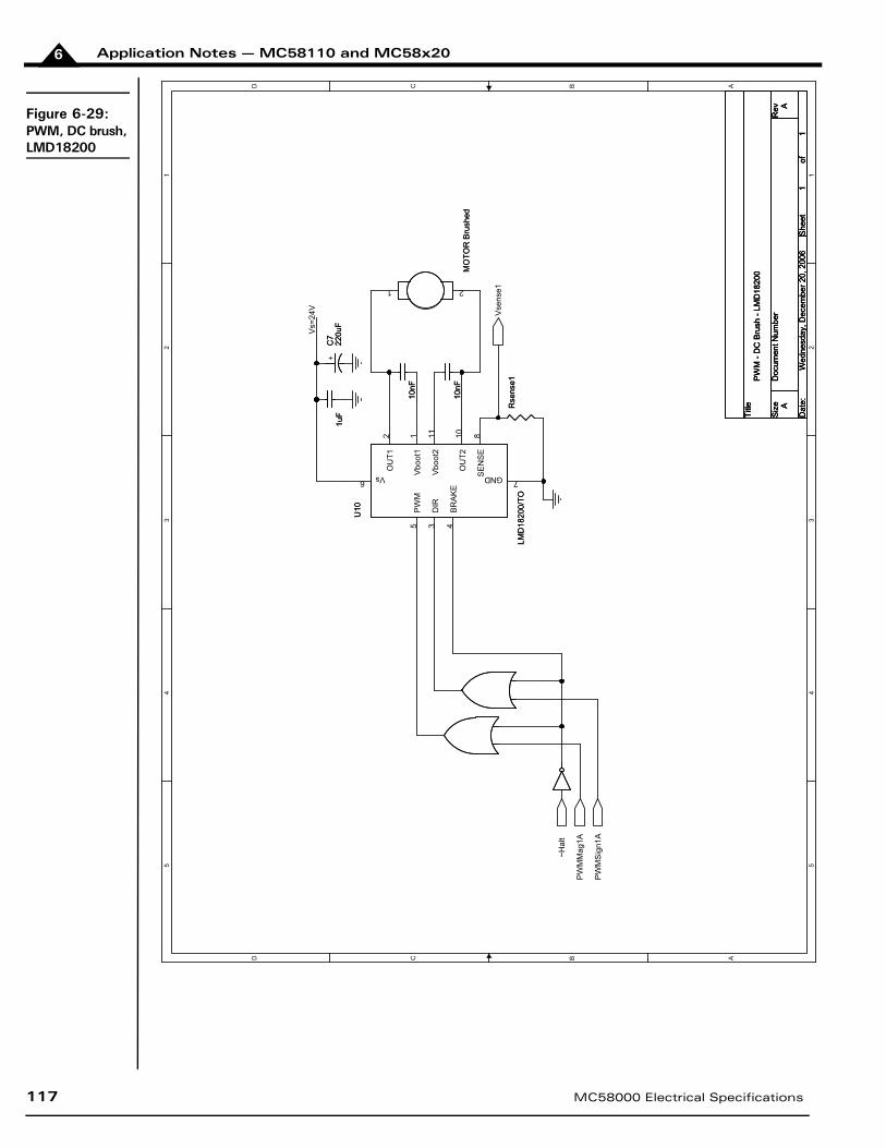
Application Notes — MC58110 and MC58x206
Figure 6-29:PWM, DC brush, LMD18200
5 5
4 4
3 3
2 2
1 1
DD
CC
BB
AA
Vs=
24V
~Hal
t
Vse
nse1
PW
MM
ag1A
PW
MS
ign1
A
Title
Siz
eD
ocum
ent N
umbe
rR
ev
Dat
e:S
heet
of
A
PW
M -
DC
Bru
sh -
LMD
1820
0
A
11
Wed
nesd
ay, D
ecem
ber 2
0, 2
006
Title
Siz
eD
ocum
ent N
umbe
rR
ev
Dat
e:S
heet
of
A
PW
M -
DC
Bru
sh -
LMD
1820
0
A
11
Wed
nesd
ay, D
ecem
ber 2
0, 2
006
Title
Siz
eD
ocum
ent N
umbe
rR
ev
Dat
e:S
heet
of
A
PW
M -
DC
Bru
sh -
LMD
1820
0
A
11
Wed
nesd
ay, D
ecem
ber 2
0, 2
006
10nF
10nF
1uF
1uF
10nF
10nF
U10
LMD
1820
0/TO
U10
LMD
1820
0/TO
BR
AK
E4
SE
NS
E8
Vbo
ot1
1
Vbo
ot2
11
PW
M5
DIR
3
OU
T12
OU
T210
Vs6 GND 7
MO
TOR
Bru
shed
MO
TOR
Bru
shed
1 2
Rse
nse1
Rse
nse1
+C
722
0uF
+C
722
0uF
117 MC58000 Electrical Specifications
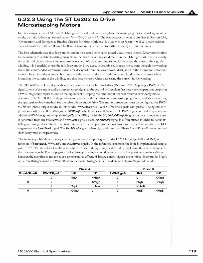
Application Notes — MC58110 and MC58x20 6
6.22.3 Using the ST L6202 to DriveMicrostepping Motors
In this example a pair of ST L6202 H-bridges are used to drive a two-phase microstepping motor in voltage-control mode, with the following nominal values: Vs = 24V, Imax = 2A. The overcurrent protection circuitry in Section 6.16, “Overcurrent and Emergency Braking Circuits for Motor Drivers,” is used with an Rsense = 0.15 power resistor. Two schematics are shown (Figure 6-30 and Figure 6-31), which utilize different decay current methods.
The first schematic uses fast decay mode, and in the second schematic, mixed-decay mode is used. Decay mode refers to the manner in which circulating currents in the motor windings are directed in the H-bridge. Fast decay is usually the preferred choice when a fast response is needed. When attempting to quickly decrease the current through the winding, it is beneficial to use the fast decay mode. Slow decay is desirable as long as the current through the winding tracks the commanded waveform, since slow decay will result in lower power dissipation in the motor and smoother motion. In a mixed decay mode, both types of the decay modes are used. For example, slow decay is used when increasing the current in the winding, and fast decay is used when decreasing the current in the winding.
The ST L6202 is an H-bridge, with separate controls for each of its halves (IN1 and IN2). Applying a PWM 50/50 signal to one of the inputs and a complementary signal to the second will result in fast decay mode operation. Applying a PWM magnitude signal to one of the inputs while keeping the other input low will result in slow decay mode operation. The MC58000 family provides an easy method of controlling a microstepping motor, and also for setting the appropriate decay method for the mixed-decay mode drive. The motion processor must be configured for PWM 50/50 two-phase output mode. In this mode, PWMMagA/B are PWM 50/50 sine signals with phase A being offset to (in advance of) phase B by 90 degrees. PWMMagC, which carries a 50% duty cycle PWM signal, is used to generate an additional PWM magnitude signal (XMagA/B) by XORing it with the 50/50 PWMMagA/B signals. A decay mode indicator is generated from the PWMSignA and PWMSignB signals. Each PWMSignA/B signal is differentiated in order to detect its falling and rising edges. The differentiated signals are then applied to the asynchronous reset and set inputs of a D-FF to generate the FastA/SlowB signal. The FastA/SlowB signal, when high, indicates that Phase A and Phase B are in fast and slow decay modes, respectively.
The following table shows the logic which generates the input signals to the L6202 H-bridge, IN1 and IN2, as a function of FastA/SlowB, PWMSignA, and PWMSignB signals. In the reference schematic the logic is implemented using a pair of 74AC153 dual 4-to-1 multiplexers. More efficient designs may be derived by exploiting the inter-relations of the different signals. The propagation delay through the logic should be kept as small as possible to reduce delays between the two phases and to reduce asynchronous effects. H-bridge control signals are in mixed-decay mode. MagA is the PWMMagA signal in PWM 50/50 mode, while XMagA is the PWM signal in Sign/Magnitude mode.
Phase A Phase BFastA/SlowB PWMSignA IN1 IN2 PWMSignB IN1 IN2
1 0 MagA ~MagA 0 L XMagB0 0 L XMagA 1 MagB ~MagB1 1 MagA ~MagA 1 XMagB L0 1 XMagA L 0 MagB ~MagB
MC58000 Electrical Specifications 118
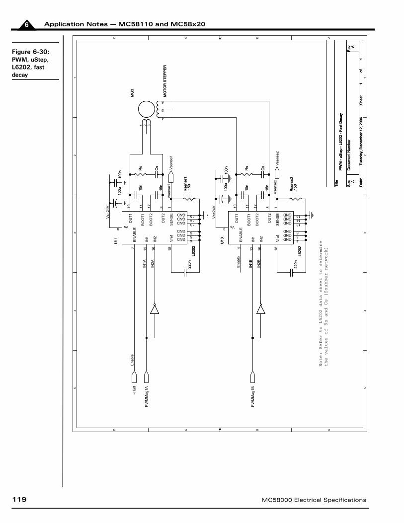
Application Notes — MC58110 and MC58x206
Figure 6-30:PWM, uStep, L6202, fast decay
5 5
4 4
3 3
2 2
1 1
DD
CC
BB
AA
Ena
ble
Vs=
24V
IN2A
Ena
ble
IN1B
IN1B
IN2B
Vs=
24V
Vse
nse1
Vse
nse2
IN1A
~Hal
t
PW
MM
ag1B
PW
MM
ag1A
Vse
nse1
Vse
nse2
Title
Siz
eD
ocum
ent N
umbe
rR
ev
Dat
e:S
heet
of
A
PW
M -
uSte
p - L
6202
- Fa
st D
ecay
A
11
Tues
day,
Dec
embe
r 12,
200
6
Title
Siz
eD
ocum
ent N
umbe
rR
ev
Dat
e:S
heet
of
A
PW
M -
uSte
p - L
6202
- Fa
st D
ecay
A
11
Tues
day,
Dec
embe
r 12,
200
6
Title
Siz
eD
ocum
ent N
umbe
rR
ev
Dat
e:S
heet
of
A
PW
M -
uSte
p - L
6202
- Fa
st D
ecay
A
11
Tues
day,
Dec
embe
r 12,
200
6
Note: Refer to L6202 data sheet to determine
the values of Rs and Cs (Snubber network)
U13
L620
2
U13
L620
2
Vre
f18
SE
NS
E1
BO
OT1
11
BO
OT2
17IN
216
EN
AB
LE2
OU
T110
OU
T28
Vs9
GND 5GND 6
GND 4IN1
12
GND 13GND 14GND 15
220n
220n
15n
15n
Cs
Cs
Rs
Rs
100n
100n
Cs
Cs
15n
15n
Rse
nse2
.150
Rse
nse2
.150
100n
100n
Rse
nse1
.150
Rse
nse1
.150
MG
3
MO
TOR
STE
PP
ER
MG
3
MO
TOR
STE
PP
ER
1 2 3
4
5
6
100u
100u
15n
15n
220n
220n
15n
15n
100u
100u
U11
L620
2
U11
L620
2
Vre
f18
SE
NS
E1
BO
OT1
11
BO
OT2
17IN
216
EN
AB
LE2
OU
T110
OU
T28
Vs9
GND 5GND 6
GND 4IN1
12
GND 13GND 14GND 15
Rs
Rs
119 MC58000 Electrical Specifications
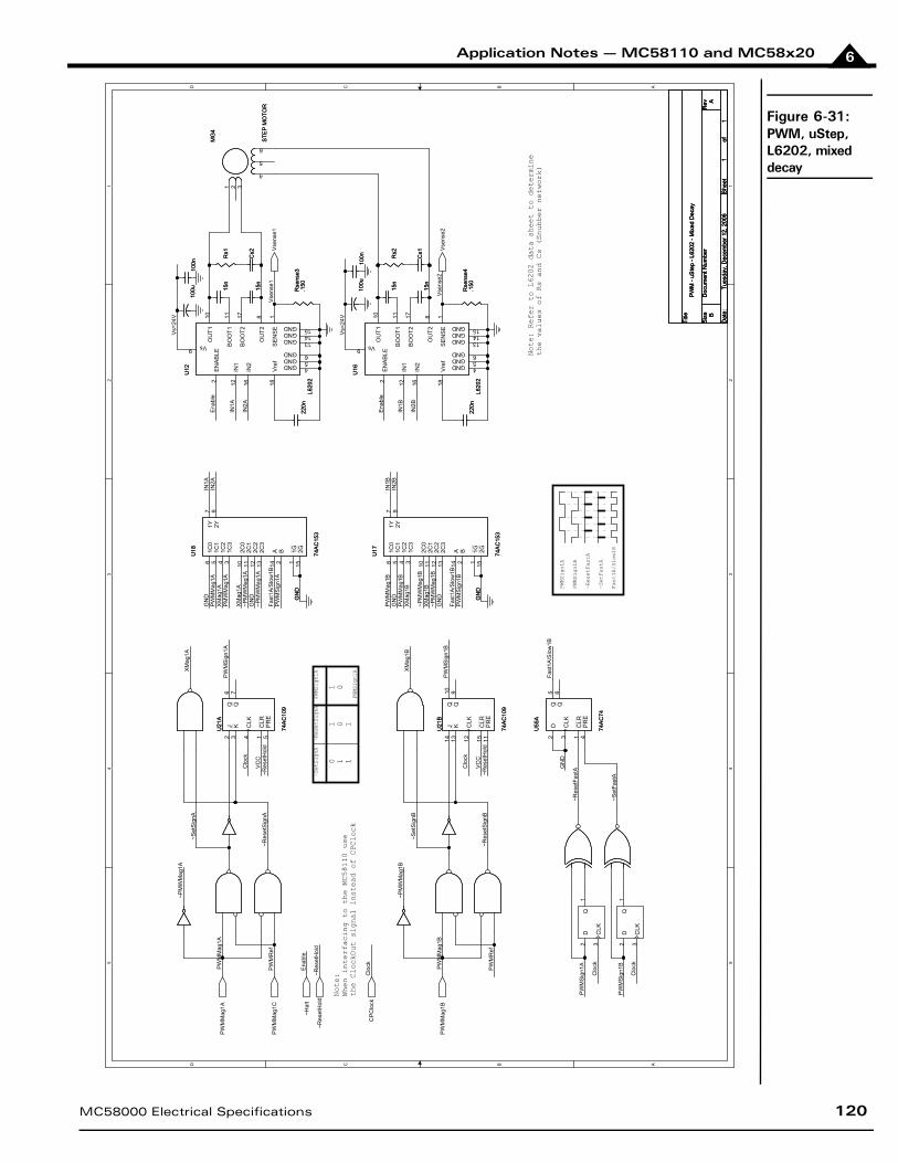
Application Notes — MC58110 and MC58x20 6
Figure 6-31:PWM, uStep, L6202, mixed decay
5 5
4 4
3 3
2 2
1 1
DD
CC
BB
AA
Ena
ble
Ena
ble
Vs=
24V
IN1A
IN2A
Ena
ble
PW
MR
ef
IN1B
IN2B
PW
MM
ag1A
XM
ag1A
~PM
WM
ag1A
~Res
etS
ignA
Vs=
24V
Vse
nse1
Vse
nse2
GN
DG
ND
Fast
1A/S
low
1B
IN1A
IN2A
PW
MS
ign1
A
GN
DP
WM
Mag
1AX
Mag
1AP
MW
Mag
1A
XM
ag1A
~PM
WM
ag1A
~PM
WM
ag1A
GN
D
PW
MS
ign1
B
XM
ag1B
GN
DG
ND
Fast
1A/S
low
1B
IN1B
IN2B
PW
MM
ag1B
GN
DP
WM
Mag
1B
GN
D
~PM
WM
ag1B
XM
ag1B
~PM
WM
ag1B
Clo
ck
~Res
etH
old
VC
C
~Set
Sig
nA
PW
MS
ign1
A
Clo
ck
~Res
etH
old
~Res
etH
old
PW
MR
ef
PW
MM
ag1B
XM
ag1B
~PM
WM
ag1B
~Res
etS
ignB
PW
MS
ign1
B
VC
C
~Set
Sig
nB
Clo
ck
PW
MS
ign1
A
Clo
ck
GN
D
PW
MS
ign1
B
Clo
ck
~Set
Fast
A
Fast
1A/S
low
1B
~Res
etFa
stA
PW
MM
ag1B
PW
MM
ag1A
~Hal
t
CP
Clo
ck
~Res
etH
old
PW
MM
ag1C
Vse
nse1
Vse
nse2
Title
Siz
eD
ocum
ent N
umbe
rR
ev
Dat
e:S
heet
of
A
PW
M -
uSte
p - L
6202
- M
ixed
Dec
ay
B
11
Tues
day,
Dec
embe
r 12,
200
6
Title
Siz
eD
ocum
ent N
umbe
rR
ev
Dat
e:S
heet
of
A
PW
M -
uSte
p - L
6202
- M
ixed
Dec
ay
B
11
Tues
day,
Dec
embe
r 12,
200
6
Title
Siz
eD
ocum
ent N
umbe
rR
ev
Dat
e:S
heet
of
A
PW
M -
uSte
p - L
6202
- M
ixed
Dec
ay
B
11
Tues
day,
Dec
embe
r 12,
200
6
~Set
Sign
A ~
Rese
tSig
nA
PWMS
ign1
A
0 1 1
1 0 0
1 1
PWMS
ign1
A
PWMS
ign1
A
PWMS
ign1
B
~Res
etFa
stA
Fast
1A/S
low1
B
~Set
Fast
A
Note:
When interfacing to the MC58110 use
the ClockOut signal instead of CPClock
Note: Refer to L6202 data sheet to determine
the values of Rs and Cs (Snubber network)
U16
L620
2
U16
L620
2
Vre
f18
SE
NS
E1
BO
OT1
11
BO
OT2
17IN
216
EN
AB
LE2
OU
T110
OU
T28
Vs9
GND 5GND 6
GND 4IN1
12
GND 13GND 14GND 15
220n
220n
15n
15n
Rse
nse4
.150
Rse
nse4
.150
100u
100u
Rse
nse3
.150
Rse
nse3
.150
U17
74A
C15
3
U17
74A
C15
3
1C0
61C
15
1C2
41C
33
2C0
102C
111
2C2
122C
313
A14
B2
1Y7
2Y9
1G1
2G15
Rs1
Rs1
15n
15n
Cs1
Cs1
U55
A
74A
C74
U55
A
74A
C74
CLR
1
D2
CLK
3
PR
E4
Q5
Q6
100u
100u
U21
B
74A
C10
9
U21
B
74A
C10
9
CLR
15
J14
K13
CLK
12
PR
E11
Q10
Q9
Q1
D2
CLK
3
Rs2
Rs2
U21
A
74A
C10
9
U21
A
74A
C10
9
CLR
1
J2
K3
CLK
4
PR
E5
Q6
Q7
MG
4
STE
P M
OTO
R
MG
4
STE
P M
OTO
R
1 2 3
4
5
6
U18
74A
C15
3
U18
74A
C15
3
1C0
61C
15
1C2
41C
33
2C0
102C
111
2C2
122C
313
A14
B2
1Y7
2Y9
1G1
2G15
220n
220n
Cs2
Cs2
100n
100n
Q1
D2
CLK
3
15n
15n
100n
100n
15n
15n
U12
L620
2
U12
L620
2
Vre
f18
SE
NS
E1
BO
OT1
11
BO
OT2
17IN
216
EN
AB
LE2
OU
T110
OU
T28
Vs9
GND 5GND 6
GND 4IN1
12
GND 13GND 14GND 15
MC58000 Electrical Specifications 120
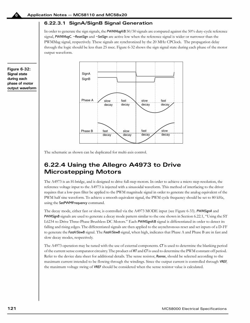
Application Notes — MC58110 and MC58x206
6.22.3.1 SignA/SignB Signal Generation
In order to generate the sign signals, the PWMMagA/B 50/50 signals are compared against the 50% duty-cycle reference signal, PWMMagC. ~ResetSign and ~SetSign are active low when the reference signal is wider or narrower than the PWMMag signal, respectively. These signals are synchronized by the 20 MHz CPClock. The propagation delay through the logic should be less than 25 nsec. Figure 6-32 shows the sign signal state during each phase of the motor output waveform.
Figure 6-32:Signal state during each phase of motor output waveform
The schematic as shown can be duplicated for multi-axis control.
6.22.4 Using the Allegro A4973 to Drive Microstepping Motors
The A4973 is an H-bridge, and is designed to drive full-step motors. In order to achieve a micro step resolution, the reference voltage input to the A4973 is injected with a sinusoidal waveform. This method of interfacing to the driver requires that a low-pass filter be applied to the PWM magnitude signal in order to generate the analog equivalent of the PWM half sine waveform. To achieve a smooth equivalent signal, the PWM cycle frequency should be set to 80 kHz, using the SetPWMFrequency command.
The decay mode, either fast or slow, is controlled via the A4973 MODE input (see Figure 6-33). PWMSignA and PWMSignB signals are used to generate a decay mode pattern similar to the one shown in Section 6.22.1, “Using the ST L6234 to Drive Three-Phase Brushless DC Motors.” Each PWMSignA/B signal is differentiated in order to detect its falling and rising edges. The differentiated signals are then applied to the asynchronous reset and set inputs of a D-FF to generate the FastA/SlowB signal. The FastA/SlowB signal, when high, indicates that Phase A and Phase B are in fast and slow decay modes, respectively.
The A4973 operation may be tuned with the use of external components. CT is used to determine the blanking period of the current sense comparator circuitry. The product of RT and CT is used to determine the PWM constant off period. Refer to the device data sheet for additional details. The sense resistor, Rsense, should be selected according to the maximum current intended to be flowing through the windings. Since the output current is controlled through VREF, the maximum voltage swing of VREF should be considered when the sense resistor value is calculated.
121 MC58000 Electrical Specifications
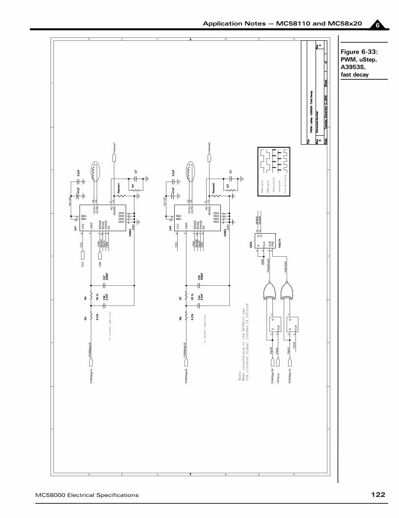
Application Notes — MC58110 and MC58x20 6
Figure 6-33:PWM, uStep, A3953S, fast decay
5 5
4 4
3 3
2 2
1 1
DD
CC
BB
AA
VC
C
~Hal
t
GN
DS
ignA
Mod
eA
VC
C
~Hal
t
GN
DS
ignB
Mod
eB
Vs=
12V
PW
MM
ag1A
GN
D
PW
MM
ag1B
~Res
etFa
stA
GN
D
Sig
nA
Clo
ck
~Set
Fast
A
Mod
eA
Sig
nB
Clo
ck
Mod
eB
Vs=
12V
GN
D
~Hal
t
VC
C
PW
MM
ag1A
PW
MM
ag1B
Vse
nse1
Vse
nse2
PW
MS
ign1
B
PW
MS
ign1
A
CP
Clo
ck
Title
Siz
eD
ocum
ent N
umbe
rR
ev
Dat
e:S
heet
of
A
PW
M -
uSte
p - A
3953
S -
Fast
Dec
ay
B
11
Tues
day,
Dec
embe
r 12,
200
6
Title
Siz
eD
ocum
ent N
umbe
rR
ev
Dat
e:S
heet
of
A
PW
M -
uSte
p - A
3953
S -
Fast
Dec
ay
B
11
Tues
day,
Dec
embe
r 12,
200
6
Title
Siz
eD
ocum
ent N
umbe
rR
ev
Dat
e:S
heet
of
A
PW
M -
uSte
p - A
3953
S -
Fast
Dec
ay
B
11
Tues
day,
Dec
embe
r 12,
200
6
5% c
eram
ic c
apci
tors
5% c
eram
ic c
apci
tors
PWMS
ign1
A
PWMS
ign1
B
~Res
etFa
stA
Fast
1A/S
low1
B
~Set
Fast
A
Note:
When interfacing to the MC58110 use
the ClockOut signal instead of CPClock
R4
93.1
k
R4
93.1
k
0.2u
F0.
2uF
R3
9.31
k
R3
9.31
k
U41
A39
53U41
A39
53
BR
AK
E1
VR
EF
2
RC
3
PH
AS
E7
EN
8
OU
TA10
SE
NS
E11
MO
DE
14
OU
TB15
GND 4GND 5GND 12GND 13
VC
C6
VBB9 VBB16
R7
93.1
k
R7
93.1
k
C35
220p
FC
3522
0pF
CT
CT
Rse
nse2
Rse
nse2
Q1
D2
CLK
3
RT
RT
0.2u
F0.
2uF
C36
2.2n
FC
362.
2nF
U40
A39
53U40
A39
53
BR
AK
E1
VR
EF
2
RC
3
PH
AS
E7
EN
8
OU
TA10
SE
NS
E11
MO
DE
14
OU
TB15
GND 4GND 5GND 12GND 13
VC
C6
VBB9 VBB16
RT
RT
47uF
47uF
Q1
D2
CLK
3
Rse
nse1
Rse
nse1
C34
2.2n
FC
342.
2nF
R6
9.31
k
R6
9.31
k
C37
220p
FC
3722
0pF
U63
A
74A
C74
U63
A
74A
C74
CLR
1
D2
CLK
3
PR
E4
Q5
Q6
47uF
47uF
CT
CT
MC58000 Electrical Specifications 122
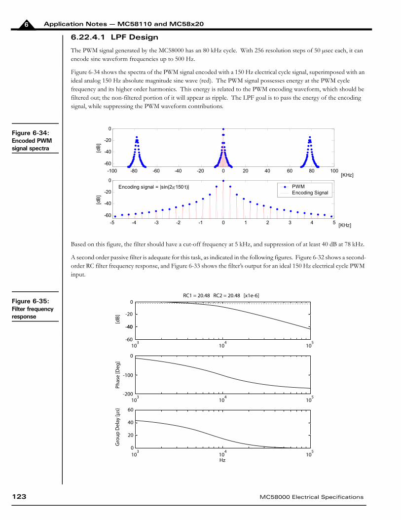
Application Notes — MC58110 and MC58x206
6.22.4.1 LPF Design
The PWM signal generated by the MC58000 has an 80 kHz cycle. With 256 resolution steps of 50 µsec each, it can encode sine waveform frequencies up to 500 Hz.
Figure 6-34 shows the spectra of the PWM signal encoded with a 150 Hz electrical cycle signal, superimposed with an ideal analog 150 Hz absolute magnitude sine wave (red). The PWM signal possesses energy at the PWM cycle frequency and its higher order harmonics. This energy is related to the PWM encoding waveform, which should be filtered out; the non-filtered portion of it will appear as ripple. The LPF goal is to pass the energy of the encoding signal, while suppressing the PWM waveform contributions.
Figure 6-34:Encoded PWM signal spectra
Based on this figure, the filter should have a cut-off frequency at 5 kHz, and suppression of at least 40 dB at 78 kHz.
A second order passive filter is adequate for this task, as indicated in the following figures. Figure 6-32 shows a second-order RC filter frequency response, and Figure 6-33 shows the filter’s output for an ideal 150 Hz electrical cycle PWM input.
Figure 6-35:Filter frequency response
-100 -80 -60 -40 -20 0 20 40 60 80 100
-60
-40
-20
0
[KHz]
[dB
]
-5 -4 -3 -2 -1 0 1 2 3 4 5
-60
-40
-20
0
[dB
]
PWMEncoding Signal
[KHz]
Encoding signal = |sin(2.150.t)|
123 MC58000 Electrical Specifications
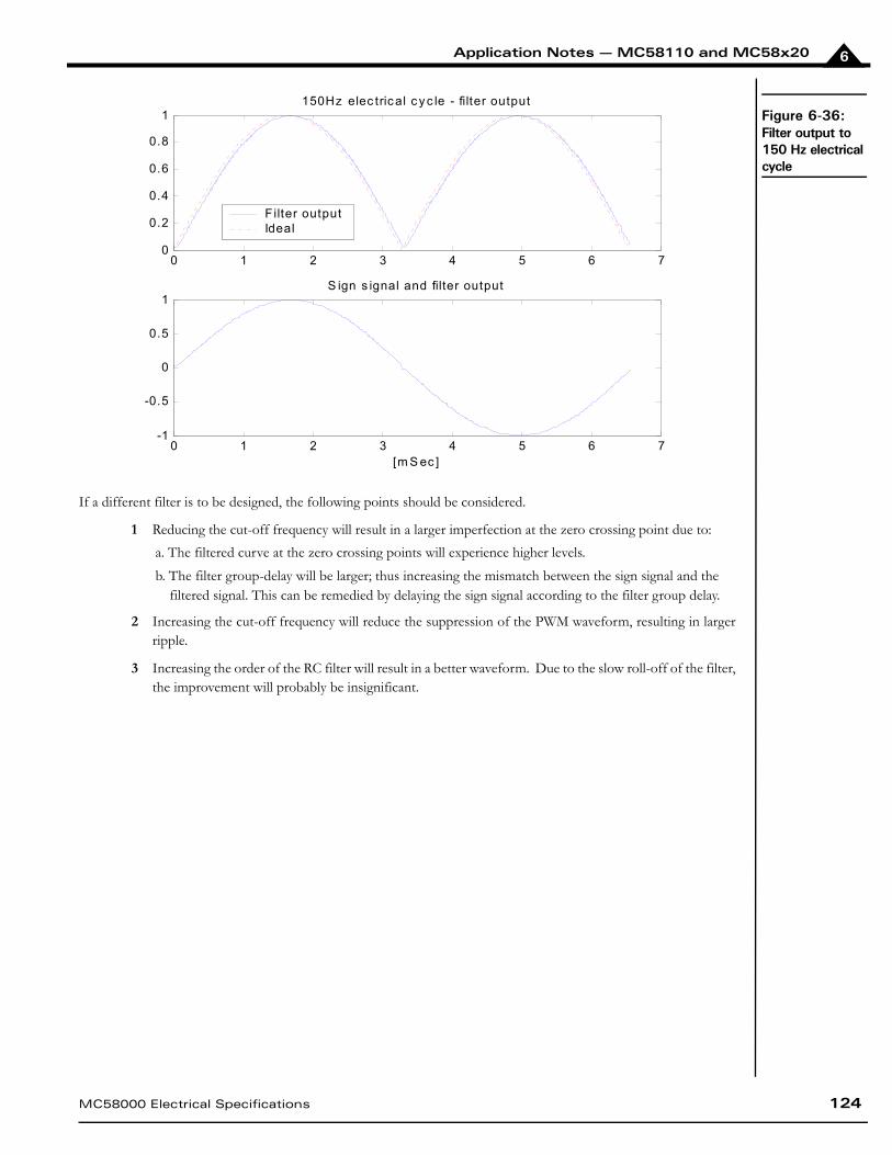
Application Notes — MC58110 and MC58x20 6
Figure 6-36:Filter output to 150 Hz electrical cycle
If a different filter is to be designed, the following points should be considered.
1 Reducing the cut-off frequency will result in a larger imperfection at the zero crossing point due to:
a. The filtered curve at the zero crossing points will experience higher levels.
b. The filter group-delay will be larger; thus increasing the mismatch between the sign signal and the filtered signal. This can be remedied by delaying the sign signal according to the filter group delay.
2 Increasing the cut-off frequency will reduce the suppression of the PWM waveform, resulting in largerripple.
3 Increasing the order of the RC filter will result in a better waveform. Due to the slow roll-off of the filter,the improvement will probably be insignificant.
0 1 2 3 4 5 6 70
0.2
0.4
0.6
0.8
1150Hz elec trical c y c le - filter output
0 1 2 3 4 5 6 7-1
-0.5
0
0.5
1S ign s ignal and filter output
[m S ec ]
F ilter outputIdeal
MC58000 Electrical Specifications 124

Application Notes — MC58110 and MC58x206
6.23 Using the Allegro A3977 to Drive Microstepping MotorsThe A3977 is a complete microstepping motor driver with a built-in translator. The translator is capable of driving bi-polar stepper motors in full-, half-, quad-, and eighth-step modes. When the step input transitions from low to high, the A3977 will advance the motor one full-, half-, quad-, or eighth-step according to the configuration of the MS1 and MS2 pins. In the example the driver is configured for eighth-step resolution.
The A3977 operation can be tuned with the use of external components. CT is used to determine the blanking period of the current sense comparator circuitry. The product of RT and CT is used to determine the PWM constant off period. R1 and R2, along with RT and CT, determine the percentage of the fast decay in mixed decay mode. The sense resistors, Rsense, should be selected according to the maximum current and voltage restrictions of the driver. Refer to the device data sheet for further information.
For a direct interface of the pulse signal to the step input, the polarity of the pulse signal must be inverted using the SetSignalSense command. This is required because the A3977 recognizes a step during a low-to-high transition of the step input signal, whereas the non-inverted behavior of the MC58000 is to generate a step on a high-to-low transition. The pulse and direction outputs will satisfy the A3977 timing requirements if operated at a step rate of 155.625 kHz or less. This can be set using the SetStepRange command. The MC58110 has a maximum step rate of 97.6 kHz.
The schematic in Figure 6-37 uses the sense outputs to detect a malfunction by sensing the current through the motor windings. To generate the ~Halt signal, the over-current circuitry should be configured with an Rsense = 0.15 power resistor for a rated 2A motor.
125 MC58000 Electrical Specifications
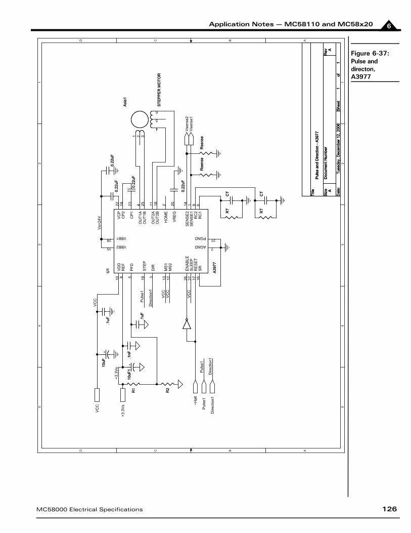
Application Notes — MC58110 and MC58x20 6
Figure 6-37:Pulse and directon, A3977
5 5
4 4
3 3
2 2
1 1
DD
CC
BB
AA
Pul
se1
Dire
ctio
n1
Pul
se1
VC
C
Dire
ctio
n1
Vs=
24V
+3.3
Vs
VC
C
VC
C
VC
C
~Hal
t
Vse
nse2
Vse
nse1
Pul
se1
Dire
ctio
n1
VC
C
+3.3
Vs
Title
Siz
eD
ocum
ent N
umbe
rR
ev
Dat
e:S
heet
of
A
Pul
se a
nd D
irect
ion
- A39
77
A
11
Tues
day,
Dec
embe
r 12,
200
6
Title
Siz
eD
ocum
ent N
umbe
rR
ev
Dat
e:S
heet
of
A
Pul
se a
nd D
irect
ion
- A39
77
A
11
Tues
day,
Dec
embe
r 12,
200
6
Title
Siz
eD
ocum
ent N
umbe
rR
ev
Dat
e:S
heet
of
A
Pul
se a
nd D
irect
ion
- A39
77
A
11
Tues
day,
Dec
embe
r 12,
200
6
R1
R1
.1uF
.1uF
+10
uF1
+10
uF1
RT
RT
0.22
uF0.
22uF
0.22
uF0.
22uF
0.22
uF0.
22uF
Rse
nse
Rse
nse
.1uF
.1uF
0.22
uF0.
22uF
CT
CT
R2
R2
.1nF
.1nF
CT
CT
+10
uF+
10uF
U1
A39
77
U1
A39
77
OU
T1A
4O
UT1
B25
RC
16
OU
T2B
18O
UT2
A11
SE
NS
E1
1S
EN
SE
214
STE
P19
DIR
3
MS
212
MS
113
VBB215
VD
D10
VBB128
RC
29
PFD
5
SR
16R
ES
ET
17
VR
EG
20
CP
123
CP
224
VC
P22
HO
ME
2
EN
AB
LE26
SLE
EP
27
AGND 7
PGND 21
RE
F8
Axi
s1
STE
PP
ER
MO
TOR
Axi
s1
STE
PP
ER
MO
TOR
1 2 3
4
5
6
Rse
nse
Rse
nse
RT
RT
MC58000 Electrical Specifications 126

Application Notes — MC58110 and MC58x206
This page intentionally left blank.
127 MC58000 Electrical Specifications

MC58000 Electrical Specifications 128
For additional information, or for technical assistance,please contact PMD at (781) 674-9860.
You may also e-mail your request to [email protected]
Visit our website at http://www.pmdcorp.com
Performance Motion Devices55 Old Bedford Rd.Lincoln, MA 01773