Embed Size (px)
Citation preview

Seediscussions,stats,andauthorprofilesforthispublicationat:https://www.researchgate.net/publication/313592329
LP-HLS:AutomaticPower-IntentGenerationforHigh-LevelSynthesisBasedHardwareImplementationFlow
ArticleinMicroprocessorsandMicrosystems·February2017
DOI:10.1016/j.micpro.2017.02.002
CITATIONS
2
READS
109
4authors:
Someoftheauthorsofthispublicationarealsoworkingontheserelatedprojects:
PhDresearchViewproject
HLSbasedVLSIimplementationsofMultimediaVideoCodingViewproject
AffaqQamar
AbasynUniversity
13PUBLICATIONS14CITATIONS
SEEPROFILE
F.B.Muslim
PolitecnicodiTorino
7PUBLICATIONS11CITATIONS
SEEPROFILE
JavedIqbal
PolitecnicodiTorino
8PUBLICATIONS7CITATIONS
SEEPROFILE
LucianoLavagno
PolitecnicodiTorino
202PUBLICATIONS7,176CITATIONS
SEEPROFILE
AllcontentfollowingthispagewasuploadedbyAffaqQamaron27February2017.
Theuserhasrequestedenhancementofthedownloadedfile.

Microprocessors and Microsystems 50 (2017) 26–38
Contents lists available at ScienceDirect
Microprocessors and Microsystems
journal homepage: www.elsevier.com/locate/micpro
LP-HLS: Automatic power-intent generation for high-level synthesis
based hardware implementation flow
Affaq Qamar a , ∗, Fahad Bin Muslim
b , Javed Iqbal b , Luciano Lavagno
b
a Department of Electrical Engineering, Abasyn University, Pakistan b Department of Electronics and Telecommunication (DET), Politecnico di Torino, Italy
a r t i c l e i n f o
Article history:
Received 5 May 2016
Revised 21 November 2016
Accepted 6 February 2017
Available online 10 February 2017
Additional Key Words and Phrases:
High-level synthesis
RTL
Design space exploration
Common power format
Low power designs
Design automation
EDA methodologies
a b s t r a c t
The abstraction level for digital designs is rising from Register Transfer Level (RTL) to algorithmic untimed
or transaction-based, followed by an automated high-level synthesis (HLS) flow. However, it is still a sig-
nificant challenge for chip architects and designers to describe low-power design decisions at the system-
level. Nowadays, low power design techniques for digital blocks are applied at RTL and there exists no
commercial tool or methodology that can automatically derive the power intent from the system-level
description. The process requires considerable amount of human intervention and various low-level de-
tails that are needed to implement low power schemes at RTL. This research aims to integrate low power
techniques, specifically Power Shut-Off (PSO), within a model-based hardware flow and to derive an au-
tomated Low Power-High Level Synthesis (LP-HLS) methodology. The methodology aims at minimizing
the design effort for low power design by deriving low-level power intent automatically for model-based
designs, while using high-level synthesis to achieve a broad set of target system implementations. LP-HLS
uses set of pragmas and a directive file to derive power intent information. To illustrate the methodology,
three model designs, ranging from simple designs to medium complexity hardware accelerators, are con-
sidered. Finally, the power saving results for the design scenarios validate the effectiveness of our LP-HLS
methodology.
© 2017 Elsevier B.V. All rights reserved.
V
d
1
c
t
s
s
a
B
s
k
a
m
t
w
1. Introduction
System-on-chip (SoC) designs are becoming increasingly het-
erogeneous as they combine multicore architectures with a va-
riety of hardware accelerators to carry out dedicated computa-
tional tasks. These hardware accelerators offer several orders-of-
magnitude higher power and timing efficiency than a correspond-
ing software implementation [1] . However, the presence of accel-
erators aggravates the complexity of SoC design. Moreover, digital
designers aim at developing designs that optimize both timing and
power, which generally are two conflicting performance objectives.
Pareto-optimality can be comfortably achieved only if power speci-
fication is considered at the system-level. This is because major ar-
chitectural decisions related to cost (area), performance and energy
utilization can be made only at higher abstraction levels [2] . For
example, parallelism versus voltage and clock frequency is much
easier to trade off at system-level. Early consideration of effective
power management helps relieve the power bottlenecks of today’s
∗ Corresponding author.
E-mail address: [email protected] (A. Qamar).
h
o
d
r
T
http://dx.doi.org/10.1016/j.micpro.2017.02.002
0141-9331/© 2017 Elsevier B.V. All rights reserved.
LSI design, enabling sustained high-performance operation with
esired power consumption levels.
.1. Model-based designs
As far as behavioral description for the hardware design is con-
erned, the abstraction level is rising from RTL to algorithmic un-
imed or transaction-based, followed by an automated high-level
ynthesis (HLS) flow [3] . HLS takes as input the model-based de-
cription of the design, specified in some high-level language such
s C, C ++ , SystemC or Simulink, and synthesizes it to generate RTL.
y elaborating different sets of constraints, HLS tools allow de-
igners to evaluate multiple implementation alternatives, a process
nown as Design Space Exploration (DSE) [26,27] . DSE with HLS is
lready a major leap from DSE with Logic Synthesis, since the for-
er can be achieved by simply changing HLS tool directives, while
he latter usually requires one to manually change a detailed hard-
are description expressed in the form of Verilog or VHDL. Such
ardware descriptions at a lower abstraction level are often tried
nly for one or two architectural options, due to the much slower
esign and verification cycle [34] . Also, high design productivity
equires that complex SoCs consist of 90% reused components [4] .
his in turn requires soft IP components, which are designed once

A. Qamar et al. / Microprocessors and Microsystems 50 (2017) 26–38 27
u
t
1
h
i
c
a
t
n
m
d
a
h
r
h
f
t
t
a
g
a
t
1
t
a
T
f
t
d
S
s
s
t
t
C
t
t
w
E
c
a
u
p
A
l
v
e
t
t
p
s
T
s
w
d
p
d
t
i
r
S
2
o
a
p
H
a
m
d
c
e
a
t
s
l
e
o
f
t
e
f
t
w
n
S
M
t
l
o
t
l
c
i
c
q
u
V
f
I
a
d
t
t
a
t
sing high-level languages and implemented into various instances
o meet the changing design requirements [5] .
.2. Low power design flow
As far as functional description of hardware is concerned, it
as evolved to the extent that model-based design approaches us-
ng automated HLS flows have gained popularity within the design
ommunity [6] . However, it is still a significant challenge for chip
rchitects and designers to describe low-power design decisions at
he system-level. This is because; system architects have little or
o visibility of the lower-level details that are needed to imple-
ent low power schemes at RTL [14] . Similarly, a digital back-end
esigner needs to interact intensively with the system architect
s well as with the verification team to formulate an appropriate
ardware platform and a low power scheme in order to meet the
equirements. This process still involves a considerable amount of
uman intervention, because nowadays the low power techniques
or a digital system are applied at register transfer level (RTL), and
hus the designer needs to intimately know the RTL code in order
o successfully apply them. These techniques include supply volt-
ge and clock control technologies, such as power shut-down, clock
ating, dynamic voltage and frequency scaling, and adaptive volt-
ge scaling [7] . The power shut-down technology is especially vital
o leakage power reduction for battery-driven devices.
.3. Contribution
This research aims to integrate the aforementioned low power
echniques within a model-based hardware flow and to derive an
utomated Low Power High-Level Synthesis (LP_HLS) methodology.
his methodology enables the specification of both the behavioral
unctionality and the power intent at a level of abstraction higher
han RTL and the use of HLS tools at the front-end of the ensuing
esign flow.
The behavioral description of the design can be captured using
ystemC or C/C ++ , although in this paper we use SystemC for the
ake of illustration. In our proposed flow, the power intent , i.e. the
et of power-saving techniques to be used and all the information
hat is needed to implement them, is automatically derived from
he system-level design using a set of pragmas and a directives file.
ombining this information with technology dependent parame-
ers, a tool that we developed derives low power intent written in
he Common Power Format (CPF), or Unified Power Format (UPF),
hich are widely used standards supported by several commercial
DA tool vendors.
In this work, we use CPF for the sake of illustration, and
onsider power shut-off (PSO) along with clock gating (CG) to
chieve power saving [10,35] . To illustrate the methodology, we
se three examples ranging from simple designs to medium com-
lexity hardware accelerators. These include a 32 bit Ripple-Carry
dder (RCA), a general purpose ALU performing arithmetic and
ogical operations, and an IDCT block often used in image and
ideo processing. Our methodology aims at minimizing the design
ffort f or low power design by deriving low-level power intent au-
omatically for model-based designs, while using high-level syn-
hesis to achieve a broad set of target system implementations. In
articular, we propose:
• A generic power management module description at the
system-level, to specify the design context of a hardware block;
• A tool that, for a given system design context automatically
generates the low power design directives needed to imple-
ment the PSO technique in the back-end flow.
• A novel LP-HLS methodology which uses an HLS tool as a front-
end environment and integrates it with a standard back-end
digital low-power flow. g
The goal is not to show an improvement in terms of power
avings with respect to the standard low-power RTL-to-GDSII flow.
he goal is to show that the same improvement can be achieved by
tarting from system level (e.g. from a SystemC, C or C ++ model),
ith very little effort, and without requiring the designer to un-
erstand the details of the automatically generated RTL code.
The rest of the paper is organized as follows. Section 2 briefly
resents the related work. Our LP-HLS methodology is explained in
etail in Section 3 . Section 4 lists our design test cases along with
he description of a sample power management module generat-
ng the signals necessary to power gate our design test cases. The
esults are presented in Section 5 while the work is concluded in
ection 6 .
. Related work
Most work on low power techniques using CPF and UPF focuses
n the RTL, rarely considering system-level implications. An ex-
mple is [9,35] , which focuses on the manual description of the
ower intent using CPF for RTL implementations generated using
LS. In this work, on the other hand, we propose a methodology to
utomatically generate the CPF power specification from a high-level
odel just like an HLS tool generates the RTL from a behavioral
escription.
Specifying power intent at the system-level results in a signifi-
ant reduction in the design effort. A system-level model is much
asier to understand than RTL due to its higher level of abstraction
nd can result in significant reduction of design effort if power op-
imization is considered at the system-level. Furthermore, the long
imulation and analysis times required while considering power at
ower levels of abstraction can be significantly reduced by consid-
ring power at the system-level [38] . Moreover, adding the power
ptimization logic at the system-level rather than at RTL makes
unctional verification easier, thanks to the design-specific SystemC
est bench.
Benini et al. [10] and Lin et al. [11] suggest various en-
rgy optimizations starting from software down to circuit-level
or electronic systems. Their strategy starts from power optimiza-
ions at system-level including energy-aware task scheduling, hard-
are/software partitioning, power aware architectures using dy-
amic power management (DPM) policies and code morphing.
imilarly, they emphasize adopting low power schemes such as
SV, PSO, CG, and DVFS at the RTL, while using gates with varying
ransistor widths to achieve additional energy saving at the gate-
evel.
Schirrmeister [12] , and Benini and Micheli [13] provide a review
f the different abstraction levels for energy measurement and es-
imation as well as common techniques to optimize a design for
ow power above RTL. They use a typical JPEG decoder as a test
ase. The authors advocate the use of a system-level solution early
n the design cycle for data-flow dominated blocks and their asso-
iated memories.
Zhang et al. [14] argues that in order to meet strict power re-
uirements, modern day designers may still have to perform man-
al optimizations on an RTL design described using Verilog or
HDL by applying numerous low power techniques considering
unctional, structural, temporal and spatial information together.
t is extremely difficult to achieve these goals manually in such
complex multi-dimensional space within a limited time. In ad-
ition, power scaling requires designers to evaluate and optimize
he system architecture as early as possible in the design flow. Cer-
ainly, the solution is to raise the level of abstraction beyond RTL to
chieve faster power optimization and to use automated RTL syn-
hesis tools.
Thus, there exists a general agreement among the designers re-
arding the significance of system-level power optimization tech-

28 A. Qamar et al. / Microprocessors and Microsystems 50 (2017) 26–38
Fig. 1. Power reduction as a function of various stages of design cycle.
Fig. 2. Overview of the low power design model.
i
t
t
t
3
#
d
i
t
d
t
t
p
f
m
p
e
i
c
t
p
fi
d
s
s
r
m
t
b
t
c
niques [29,36] . Commercial effort s in producing pre-RTL power op-
timization tools have resulted in tools such as Vista Architect from
Mentor Graphics and Chip vision’s PowerOpt ۛ, Two new working
groups were formed by IEEE at the end of 2014 to standardize
system-level power modeling for SoC devices [15] . The prospect
of considering power intent at the system-level and applying it in
combination with HLS thus is an important but rather sparsely ex-
plored area and hence a theme of this work.
3. LP-HLS methodology
The earlier energy savings are considered in the design cycle,
the more savings can be achieved, as shown in Fig. 1 . This is be-
cause architectural decisions related to cost (area), performance
and energy utilization are made at this level [37] . Considering
power optimization at a lower level of abstraction, as is the case
in a standard ASIC design flow, would require significant iterative
changes in the overall design architecture and hence a larger de-
sign effort, as depicted in Fig. 1 .
Hence, the prospect of a completely automated low power flow,
where both the logic and power intent can be incorporated into
the design at the system-level, seems very promising. In this sec-
tion, we present a complete description of our LP-HLS methodol-
ogy, which comprises an HLS flow, a CPF generator to automati-
cally produce CPF power intent, and the final integration into the
back-end flow.
3.1. Model-based hardware design
The overview of the proposed design flow is shown in Fig. 2 .
The power intent is derived by extracting the design related infor-
mation from the system-level description. This information is read
together with the power rules specification for the PSO, and the
technology related parameters to automatically generate the CFP
file. The hardware description for low power design is then inte-
grated with the RTL during the later stages of back-end flow.
Luckily, even when the RTL is generated automatically using
HLS from the system-level code written in SystemC, the nam-
ing convention of the design hierarchy, i.e. instances, signals and
ports is preserved, or names for new objects (e.g. fields of Sys-
temC struct-typed I/O signals) can be easily derived automatically
from the high-level model. Beginning with the high-level model
of a design, the HLS tool executes several tasks, namely alloca-
tion, scheduling and binding, to automatically generate an RTL im-
plementation. These tasks can be performed either simultaneously
or sequentially. However, since performing them simultaneously
would be too time-consuming, the latter option is typically chosen
[8] .
In our flow, the power intent is also derived from annotations
n the SystemC code and a design configuration file that refers only
o high-level information. This makes it easier for the design archi-
ect to select among the underlying power optimization choices,
hanks to the higher level of abstraction.
.2. CPF generation tool
Our automated CPF generation tool relies upon the use of
pragma directives in the system-level design file/s as well as a
esigner-written intent specification file, to identify power related
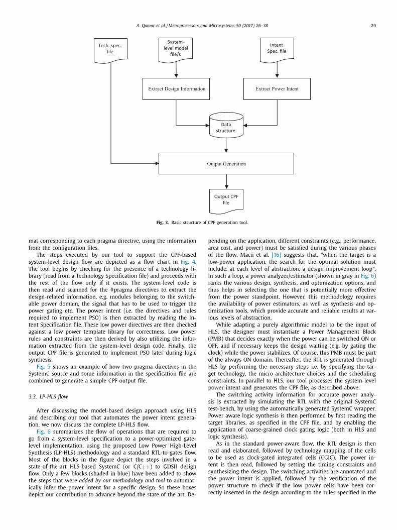
nformation. Fig. 3 shows the general structure of the tool.
The technology specification (Tech. spec. in the Fig. 3 ) file, as
he name implies, contains technology related information using
irectly the corresponding CPF syntax. In particular, it contains; (i)
he set of libraries (typically the worst, best and nominal cases), (ii)
he information about the power nets that will be created during
hysical design, and (iii) the nominal conditions (e.g. voltage levels
or various power nets) which will be used by the various power
odes afterwards.
The Intent Specification file contains pragma directives for the
ower rules that are needed to successfully implement PSO strat-
gy. These rules depend upon design related parameters. This
ncludes rules such as operating corners for multi-mode-multi-
orner (mmmc) analysis, analysis views for power domains and
he definition of power rules such as isolation, state-retention and
ower switch rules.
The CPF generator needs to extract from the system-level model
le information such as, the module name of the switchable power
omain(s), and the instance name of the signal that defines the
hut-off condition, and that will be used to drive the power
witches. This is done by inserting a #pragma directive before the
espective instance name. The tool searches for those unique prag-
as, creates token strings for the instances and stores the informa-
ion for later processing. The name of the power domain can either
e assigned by the designer (e.g. MY_DOMAIN), or be generated by
he parser (e.g. switchable_domain_ < n > ).
Once all the information from the input files is gathered into
ustom data structures, the tool generates power rules in CPF for-
A. Qamar et al. / Microprocessors and Microsystems 50 (2017) 26–38 29
Data structure
System-level model
file/s
Tech. spec. file
Extract Design Information
Intent Spec. file
Extract Power Intent
Output Generation
Output CPF file
Fig. 3. Basic structure of CPF generation tool.
m
f
s
T
b
t
t
d
a
p
r
t
a
r
m
o
s
S
c
3
a
t
g
l
S
M
s
fl
t
i
d
p
a
o
l
i
I
r
t
f
t
t
i
H
(
O
c
o
H
g
c
p
s
t
P
t
a
l
r
t
t
s
t
p
r
at corresponding to each pragma directive, using the information
rom the configuration files.
The steps executed by our tool to support the CPF-based
ystem-level design flow are depicted as a flow chart in Fig. 4 .
he tool begins by checking for the presence of a technology li-
rary (read from a Technology Specification file) and proceeds with
he rest of the flow only if it exists. The system-level code is
hen read and scanned for the #pragma directives to extract the
esign-related information, e.g. modules belonging to the switch-
ble power domain, the signal that has to be used to trigger the
ower gating etc. The power intent (i.e. the directives and rules
equired to implement PSO) is then extracted by reading the In-
ent Specification file. These low power directives are then checked
gainst a low power template library for correctness. Low power
ules and constraints are then derived by also utilizing the infor-
ation extracted from the system-level design code. Finally, the
utput CPF file is generated to implement PSO later during logic
ynthesis.
Fig. 5 shows an example of how two pragma directives in the
ystemC source and some information in the specification file are
ombined to generate a simple CPF output file.
.3. LP-HLS flow
After discussing the model-based design approach using HLS
nd describing our tool that automates the power intent genera-
ion, we now discuss the complete LP-HLS flow.
Fig. 6 summarizes the flow of operations that are required to
o from a system-level specification to a power-optimized gate-
evel implementation, using the proposed Low Power High-Level
ynthesis (LP-HLS) methodology and a standard RTL-to-gates flow.
ost of the blocks in the figure depict the steps involved in a
tate-of-the-art HLS-based SystemC (or C/C ++ ) to GDSII design
ow. Only a few blocks (shaded in blue) have been added to show
he steps that were added by our methodology and tool to automat-
cally infer the power intent for a specific design. So these boxes
epict our contribution to advance beyond the state of the art. De-
ending on the application, different constraints (e.g., performance,
rea cost, and power) must be satisfied during the various phases
f the flow. Macii et al. [16] suggests that, “when the target is a
ow-power application, the search for the optimal solution must
nclude, at each level of abstraction, a design improvement loop”.
n such a loop, a power analyzer/estimator (shown in gray in Fig. 6 )
anks the various design, synthesis, and optimization options, and
hus helps in selecting the one that is potentially more effective
rom the power standpoint. However, this methodology requires
he availability of power estimators, as well as synthesis and op-
imization tools, which provide accurate and reliable results at var-
ous levels of abstraction.
While adapting a purely algorithmic model to be the input of
LS, the designer must instantiate a Power Management Block
PMB) that decides exactly when the power can be switched ON or
FF, and if necessary keeps the design waiting (e.g. by gating the
lock) while the power stabilizes. Of course, this PMB must be part
f the always ON domain. Thereafter, the RTL is generated through
LS by performing the necessary steps i.e. by specifying the tar-
et technology, the micro-architecture choices and the scheduling
onstraints. In parallel to HLS, our tool processes the system-level
ower intent and generates the CPF file, as described above.
The switching activity information for accurate power analy-
is is extracted by simulating the RTL with the original SystemC
est-bench, by using the automatically generated SystemC wrapper.
ower aware logic synthesis is then performed by first reading the
arget libraries, as specified in the CPF file, and by enabling the
pplication of coarse-grained clock gating logic (both in HLS and
ogic synthesis).
As in the standard power-aware flow, the RTL design is then
ead and elaborated, followed by technology mapping of the cells
o be used as clock-gated integrated cells (CGIC). The power in-
ent is then read, followed by setting the timing constraints and
ynthesizing the design. The switching activities are annotated and
he power intent is applied, followed by the verification of the
ower structure to check if the low power cells have been cor-
ectly inserted in the design according to the rules specified in the

30 A. Qamar et al. / Microprocessors and Microsystems 50 (2017) 26–38
Initialize tool
Read technology file
Missing
Read system-levelsource code
Scan for pragmas
Identify low-powerinstances (signalsand modules)
Extract design info
Customdata
structure
Read low powerintent specification
file
Extract low powerintent info
Compare low-power template
library
Derive low-powerdesign rules andconstraints
TerminateOutput CPF
file
Tech. spec.file
Exit tool with error
SystemCmodel file
Yes
No
No
No
Yes
Yes
No
Intent spec.file
Fig. 4. CPF generation flow.
g
s
o
t
t
m
s
R
o
b
b
e
S
t
l
s
P
4
t
A
p
u
p
t
d
h
s
a
o
i
o
d
t
s
b
w
b
4
g
P
n
f
s
o
o
p
a
T
o
p
t
t
power intent file. Incremental optimization is performed and fi-
nally the gate-level netlist is obtained and checked for logic equiv-
alence against the input RTL.
4. Design scenarios and test cases
The example cases that are adopted are simple, yet inter-
esting enough to illustrate the proposed methodology. We start
with a simple design of a hierarchical 32 bit ripple-carry adder
(RCA) structure to better understand and apply the investigated
methodology. The module processing the 16 most significant bits
(MSB_RCA 16-31 ) is selected to be placed in a switchable power do-
main, to enable low-power processing of 16-bit numbers. Then we
move to a larger design, namely an ALU processor comprising eight
modules to perform arithmetic as well as logical operations. Here,
we choose to power down the division and multiplication modules
when they are not needed.
Memories in a SoC can be as much or even more power hun-
ry than the data path [14] . The dynamic power consumption as-
ociated with memory accesses may account for about one-third
f the total SoC power, while the remaining two-thirds come from
he clock-tree and the data path [17] . Thus, it is a good idea to also
est our methodology with a design including some arrays that are
apped to RAMs. Hence, our final design is an inverse discrete co-
ine transform (IDCT) module, which uses a significant amount of
AM resources and finds its application in JPEG decoders.
Please note that these blocks are not meant to be representative
f complex modern SOCs, but rather to be realistic SOC building
locks to which PSO and other power optimization techniques can
e meaningfully applied. Our tool and methodology can be used
qually well for larger or more numerous blocks, as long as their
ystemC models are annotated with our proposed pragmas and our
ool is used to derive the power intent.
Since our target is to test and validate the flow, we formu-
ate synthetic application scenarios for our example designs. In this
ection we discuss very briefly, the test bench setup as well as the
MB design for each.
.1. Test bench structure
The test bench setup includes a stimulus generator that drives
he input control and data signals to the design under test (DUT).
monitor block logs the outputs and checks their validity, as de-
icted in Fig. 7 .
In the case of the RCA and the ALU, the stimulus generator
ses pseudo-random number generators (PRNGs) to generate in-
ut streams as well as random values of control logic to select be-
ween the power ON and OFF conditions for the switchable power
omains. Of course, the probabilistic models should reflect the be-
avior of the real application scenarios. However, this is a well-
tudied problem that is outside the scope of this paper [31–33] .
For the RCA and the ALU, we use both a synthetic switching
ctivity profile in which the switchable domain stays ON for 10%
f the time, one in which it is ON for 90% of the time, and one
n which it is on for 50% of the time. For the IDCT design, on the
ther hand, we consider its real-life usage inside a JPEG decoder.
Please note that the PMB could be made more complex, in or-
er to require some minimum number of idle cycles before shut-
ing off the power, but again these considerations are outside the
cope of the paper [28,30] . We will see later that each transition
etween power states requires at least four clock cycles, which
ould suggest considering a threshold to trigger the transition to
e at least four cycles.
.2. Design under test (DUT)
An important issue worth considering while employing power
ating is to prevent floating states from propagating from the
ower Switchable Domain (PSD) to the default domain. It is also
ecessary to save the state of some flip-flops in the design be-
ore switching off a part of the design. Isolation cells (ISO) are re-
ponsible for isolating the always-on units from the floating values
f outputs from the power-gated units. They are typically placed
n the outputs of the shut-off power domain during the physical
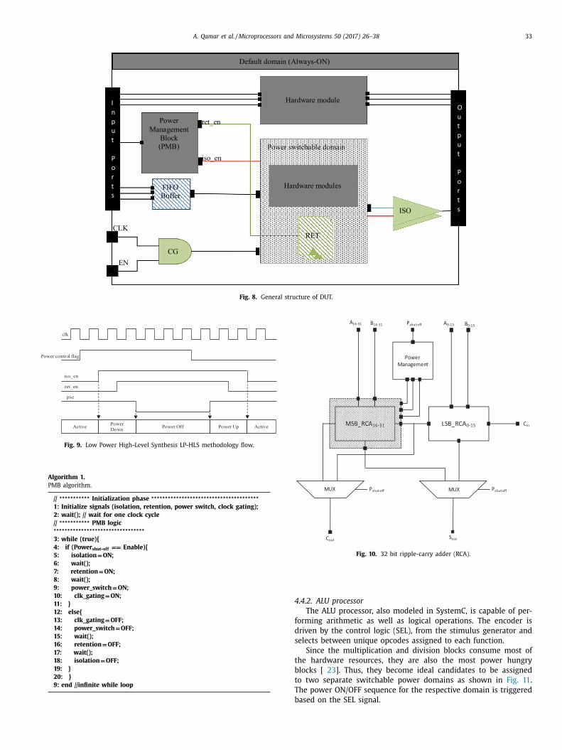
lacement stage [18] , as shown in Fig. 8 .
RET in Fig. 8 represents the state retention cells, which have the
bility to retain their states even if the primary power is shut-off.
he retention cells are optional and are needed only if the state
f some sequential logic in the power switchable domain must be
reserved. The header power switches which are inserted during
he physical implementation phase provide the ability to cut-off
he supply voltage to the switchable domain. The rules for the in-

A. Qamar et al. / Microprocessors and Microsystems 50 (2017) 26–38 31
Fig. 5. A simple example of input pragmas and corresponding CPF output.
s
p
w
t
t
i
t
t
4
a
s
a
i
t
a
t
i
c
c
T
r
t
s
s
q
f
p
a
c
t
[
i
c
o
ertion of these low power cells are stated in the power intent file
rovided to the logic synthesis tool.
In order to ensure no loss of data during the power-up process,
e chose to add a first-in-first-out (FIFO) module at the input of
he DUT, as depicted in Fig. 8 . This buffers the input values while
he module is still in the sleep mode and the data input is com-
ng in during the power-up process. Moreover, clock gating is in-
roduced by using the SystemC clock gating capability provided by
he HLS tool [22] .
.3. Power management block (PMB)
Fig. 8 also shows the PMB in the default domain. This is added
s a SystemC module to produce the control signals in the correct
equence to power gate the module instances of the power switch-
ble domain(s), as indicated in the Fig. 9 . The “Power control flag”
n Fig. 9 represents the signal in the functional model that activates
he power up/down process. This signal must be identified manu-
lly by the designer, e.g. by using activity profiling which captures
he inactivity intervals of the design and hence identifies when to
nduce power gating.
Activity profiling plays an extremely important role while
hoosing a specific power optimization strategy for a design and it
an be accomplished fairly accurately for a specific application [19] .
he analysis of inactivity periods for a specific application usually
elies on using predictive strategies either based on the past his-
ory of the idle and active states, or using the application-specific
ignal activity traces [20,21] .
During the power down process, isolation must happen before
tate retention, followed by power shut-off, while the reverse se-
uence must be followed during the power up process. The signals
or isolation, state retention and power shut-off as provided by the
ower control module are “iso_en”, “ret_en” and “pse” respectively,
s shown in Fig. 9 .
In this case the power up/down sequences consume four clock
ycles, plus the number of cycles that are required to bring
he power rails to the required supply voltage. Many surveys
13,35] suggest combining PSO with CG for maximizing power sav-
ngs. When the switchable domain is powered down, we gate its
lock nets at the time of power down. The SystemC pseudo code
f our (purely illustrative) PMB block is presented as Algorithm 1 .

32 A. Qamar et al. / Microprocessors and Microsystems 50 (2017) 26–38
To physical implementation
System-Level Power Analysis
Behavioral Power Analysis
High-Level Synthesis and Optimization
System-Level Specifications
Function Partitioning and
HW/SW Allocation
Model-based HW Description
Automatic Power Intent Generation
Low Power Architecture
Choices
Power-Driven Behavioral
Transformations
RT-LevelDescrip�on
Power Intent
Descrip�on
Low Power Logic synthesis
and Optimization
Power Conscious Gate-Level Description
Logic Equivalence
Check
Gate-Level Power Analysis
RT-Level Power Analysis
Fig. 6. Low Power High-Level Synthesis LP-HLS methodology flow.
MonitorDUT
Hardware Accelerator
Stimulus Generator
Fig. 7. General structure of test bench for design cases.
c
f
a
d
u
4.4. Hardware accelerators – test cases
This section briefly overviews the example cases used to vali-
date the proposed methodology.
4.4.1. 32 bit ripple carry adder (RCA)
In order to apply the PSO technique to the RCA, it is modeled in
SystemC as a hierarchical module, comprising of two 16 bit RCAs,
alled MSB_RCA 16-31 and LSB_RCA 0-1 in Fig. 10 . Both modules are
unctionally identical, but the MSB_RCA is assigned to the switch-
ble power domain, and hence it has a few additional ports to
rive power management operations. The output multiplexers also
se P shut-off as a select signal to choose between the valid outputs.
A. Qamar et al. / Microprocessors and Microsystems 50 (2017) 26–38 33
Default domain (Always-ON)
CGEN
CLK
FIFO Buffer
iso_en
ret_enPowerManagement
Block (PMB)
Input
Ports
ISO
RET
Power switchable domain
Hardware modules
Hardware moduleOutput
Ports
Fig. 8. General structure of DUT.
iso_en
ret_en
pse
Power control flag
Active PowerDown Power Off Power Up Active
clk
Fig. 9. Low Power High-Level Synthesis LP-HLS methodology flow.
Algorithm 1.
PMB algorithm.
// ∗∗∗∗∗∗∗∗∗∗∗ Initialization phase ∗∗∗∗∗∗∗∗∗∗∗∗∗∗∗∗∗∗∗∗∗∗∗∗∗∗∗∗∗∗∗∗∗∗∗∗∗∗∗
1: Initialize signals (isolation, retention, power switch, clock gating);
2: wait(); // wait for one clock cycle
// ∗∗∗∗∗∗∗∗∗∗∗ PMB logic ∗∗∗∗∗∗∗∗∗∗∗∗∗∗∗∗∗∗∗∗∗∗∗∗∗∗∗∗∗∗∗∗∗
3: while (true){
4: if (Power shut-off == Enable){
5: isolation = ON;
6: wait();
7: retention = ON;
8: wait();
9: power_switch = ON;
10: clk_gating = ON;
11: }
12: else{
13: clk_gating = OFF;
14: power_switch = OFF;
15: wait();
16: retention = OFF;
17: wait();
18: isolation = OFF;
19: }
20: }
9: end //infinite while loop
CinLSB_RCA0-15
Sout
MSB_RCA16-31
Power Management
Cout
Pshut-off
Pshut-offPshut-off
A16-31 B16-31 A0-15 B0-15
MUXMUX
Fig. 10. 32 bit ripple-carry adder (RCA).
4
f
d
s
t
b
t
T
b
.4.2. ALU processor
The ALU processor, also modeled in SystemC, is capable of per-
orming arithmetic as well as logical operations. The encoder is
riven by the control logic (SEL), from the stimulus generator and
elects between unique opcodes assigned to each function.
Since the multiplication and division blocks consume most of
he hardware resources, they are also the most power hungry
locks [ 23 ]. Thus, they become ideal candidates to be assigned
o two separate switchable power domains as shown in Fig. 11 .
he power ON/OFF sequence for the respective domain is triggered
ased on the SEL signal.
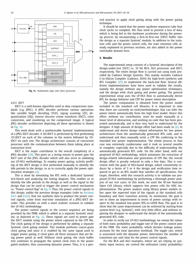
34 A. Qamar et al. / Microprocessors and Microsystems 50 (2017) 26–38
AND
OR
ADD
SUBTRACT
Shi�_L
Shi�_R
MULTIPLY
DIVIDE
Pwr_Mgt
EncoderSEL
A
B
MP
DP
EN
EN
OUT
Fig. 11. Arithemetic logic unit (ALU) processor.
e
t
c
w
u
t
t
r
s
5
d
r
v
C
R
f
n
a
e
R
i
t
p
e
l
e
d
u
a
u
i
c
t
a
p
d
d
s
d
q
t
p
y
O
p
l
b
n
s
s
s
q
g
o
o
a
i
t
t
4.4.3. IDCT
IDCT is a well-known algorithm used in data compression stan-
dards (e.g. JPEG). A JPEG decoder performs various operations
like variable length decoding (VLD), zigzag scanning (ZZ), de-
quantization (DQ), inverse discrete cosine transform (IDCT), color
conversion, and reordering on the compressed image. A typical
JPEG decoder architecture depicting all these operations is shown
in Fig. 12 .
This work deals with a synthesizable SystemC implementation
of a JPEG IDCT decoder. A 2D-IDCT is performed by first performing
1D-IDCT on each of the columns in the matrix followed by 1D-
IDCT on each row. The design architecture consists of concurrent
processes with the communication between them taking place at
transaction level.
IDCT is the major contributor to the overall complexity of a
JPEG decoder [24] . This gives us a strong reason to power gate the
IDCT unit of the JPEG decoder which will also serve in validating
our LP-HLS methodology. To employ power gating, activity profil-
ing of the IDCT design is first performed manually to identify the
idle periods in the design, so as to correctly apply the power opti-
mization strategies [2] .
This is done by simulating the RTL with a dedicated SystemC
test-bench and analyzing the timing diagram. This enables us to
identify the idle periods in the design as well as the signal in the
design that can be used to trigger the power control mechanism
i.e. “Power control flag” in Fig. 9 . Thus, the power control signals in
this design, unlike the previous design examples (refer to Sections
4.4.1 and 4.4.2 ), that use synthetic data to produce the power con-
trol signals, come from real-time simulation of a JPEG-IDCT de-
coder. This provides us with a more realistic scenario to validate
the LP-HLS methodology.
The power control signals in the correct sequence are being
provided by the PMB, which is added as a separate SystemC mod-
ule, as depicted in Fig. 12 . These signals are used to power gate
the IDCT module using the power intent captured in the CPF file.
The clock gating of the design is performed by adding a separate
SystemC clock gating module. This module performs coarse-grain
clock gating and since it is enabled by the same signal used to
trigger power gating, it clock gates all those instances that are be-
ing power gated as well. Without clock gating, the clock buffer
tree continues to propagate the system clock even to the power
gated modules, thus consuming dynamic power. Thus, it is a gen-
ral practice to apply clock gating along with the power gating
echnique.
It should be noted that the power up/down sequences take four
lock cycles to complete. We thus need to prevent a loss of data,
hich is being fed to the hardware accelerator during the power-
p process, by incorporating a first-in-first-out (FIFO) buffer into
he design as a separate SystemC module. In addition to the isola-
ion cells and the power switch cells, the state retention cells al-
eady explained in previous sections, are also added in the power
witchable domain here.
. Results
The experimental setup consists of a SystemC description of the
esign-under-test (DUT) i.e. 32 bit RCA, ALU processor, and IDCT,
espectively. The entire design flow is carried out using tools pro-
ided by Cadence Design Systems. This mainly includes Cadence
-to-Silicon Compiler (Cadence, 2014) for high-level synthesis and
TL Compiler [25] to implement the back-end flow. Several dif-
erent implementations have been used to validate the results,
amely the design without any power optimization techniques,
nd the design with clock gating and power gating. The general
xperimental setup uses the LP-HLS flow to automatically derive
TL for design behavior and CPF for power intent description.
The power computation is obtained from the power model
ncluded in the standard cell libraries. It is important to note
hat there are currently no tools/methodologies that can infer the
ower intent automatically from the high level model. Hence this
ffort, without our contribution, must be made manually at a
ower level of abstraction, and working on code that has been gen-
rated automatically, and is thus very hard to understand for the
esigner. A high amount of design effort had been made in [2] , to
nderstand and derive design related information for low power
rchitectures from the automatically generated RTL code, and to
nderstand and then manually write a CPF file conferring to the
ntended low power implementation. The whole process in that
ase was extremely cumbersome and it took us several months
o complete, especially due to the difficulty of understanding the
utomatically generated RTL code. On the other hand, with our
roposed LP-HLS methodology, which automates the extraction of
esign-related information and generation of CPF file, the overall
esign effort is greatly reduced to only a few days. This is con-
istent with the goals of HLS-based design, which consistently re-
uces by a factor of 3 or 4 the design and verification time re-
uired to get to an RTL model that satisfies all specifications. Our
arget, therefore, with this research activity is to validate our pro-
osed LP-HLS methodology by performing a thorough power anal-
sis of our test cases. In this work, we used the 45 nm NanGate
pen Cell Library, which supports low power cells for ASIC im-
lementation. The power analysis using library power models re-
ies upon the expected state of the signals at the standard cells
oundary and their transition activity. As mentioned, the goal is
ot to show an improvement in terms of power savings with re-
pect to the standard low-power RTL-to-GDSII flow. The goal is to
how that the same improvement can be achieved by starting from
ystem-level (e.g. SystemC), with very little effort, and without re-
uiring the designer to understand the details of the automatically
enerated RTL code.
In order to verify our LP-HLS methodology, we sweep the values
f both static probability and toggle rate of the power control pins
f the PMB. The static probability, which dictates leakage power,
ccounts for the total operation workload. The toggle rate, which
s associated with the dynamic power, determines the number of
ransitions per unit time for the power control signals.
For the RCA and ALU examples, where we are relying on syn-
hetic input vectors, we control the utilization (static probability)

A. Qamar et al. / Microprocessors and Microsystems 50 (2017) 26–38 35
PMB
IDCTClock Ga�ng
FIFO Module
Power Conscious IDCT Block
Compressed image data
VLD
DQ
ZZ
Re-order
Color conversi
on
Reconstructed image
Fig. 12. JPEG decoder using IDCT module.
Table 1
Power optimization of RCA w.r.t. MSB_RCA (power switchable domain).
Operations Workload
(MSB_RCA)
P static (μW) P dynamic (μW) Cell Area (μm
2 )
Without power
optimization @ 50%
70 255 Total → 3362
90% 35 104 MSB_RCA → 1051 (31%)
70% 31 97
50% 28 93
30% 25 90
Table 2
Power optimization of ALU w.r.t. DIV and MULT (power switchable domains) oper-
ations.
Operations Workload (DIV
– MULT)
P static (μW) P dynamic (μW) Cell Area (μm
2 )
Without power
optimization @ 10%–40%
190 1072 Total → 27,361
30% – 60% 140 341 DIV → 8219 (30%)
20% – 50% 133 283 MULT → 4790 (18%)
10% – 40% 129 237
1% – 10% 86 160
o
d
t
t
w
o
i
d
o
c
f
M
1
a
e
o
p
c
t
t
M
s
g
d
s
i
t
i
t
p
o
a
m
r
d
n
t
h
t
s
c
v
R
4
v
a
w
e
d
p
4
t
t
t
a
s
i
a
6
i
f the PSD by specifying a usage percentage w.r.t the rest of the
esign. The transition rate for the ON/OFF states of the power con-
rol signals is based on the utilization factor. On the other hand,
he IDCT uses real-time input vectors from the JPEG decoder, so
e keep the utilization fixed while we sweep the toggle rate to
bserve changes in dynamic power.
The power optimization result for the RCA example is presented
n Table 1 . The MSB_RCA comprises of 31% of the total size of the
esign, hence it is a good candidate for the power gating. The rest
f the design includes the PMB, LSB_RCA and two multiplexers to
ompute sum, as mentioned in Fig. 10 . The power analysis is per-
ormed for RCA without power optimization at 50% usage (i.e. the
SB_RCA is used in 50% of the clock cycles). From the graph in Fig.
3 a, it is clear that the total power consumption is almost double
s compared to the power consumption with power optimization
ven when MSB_RCA is active for 90% of the time, mainly because
f clock gating.
Similarly for the ALU, we assign the division (DIV) and multi-
lication (MULT) operations to two separate PSDs. Together, they
onstitute 48% of the total design area as mentioned in Table 2 . We
hen analyze the power consumption by assigning different utiliza-
ion to DIV and MULT. The choice of 1% usage for DIV and 10% for
ULT corresponds to a hypothetical integer workload, while the
weep between 30–10% for DIV and 60–40% of MULT can be re-
arded as a DSP workload. Fig. 13 b shows the leakage as well as
ynamic power results for the ALU. Since the cell area of the power
witchable logic is almost half of the total logic, the power saving
s even greater than in the previous example.
The IDCT design scenario uses vectors from the JPEG decoder
o obtain power results with and without power optimization, as
ndicated by the first two rows of Table 3 , respectively. The next
hree rows were obtained by increasing the toggle rate of the
ower shut-off signals to 4 times, 8 times and 32 times of the
riginal toggle rates that were obtained by simulating the RTL with
realistic usage scenario. More toggling would result in the IDCT
odule being powered on and off more frequently and this would
esult in an increase in the dynamic power consumption of the
esign while the static power remains the same. The reason for
o change in the static power is that the static probabilities of
hese pins remain the same for all the cases. The study of this be-
avior with multiple toggle rates is helpful in estimating the ex-
ent of switching beyond which any power savings would be over-
hadowed by the resulting dynamic power consumption. A visual
omparison of the effect of power optimization for the IDCT is pro-
ided in Fig. 13 c.
The total power versus RAM power and the total area versus
AM area comparison for the IDCT test case is depicted in Table
. The purpose is to demonstrate that the IDCT test case used for
alidating our methodology includes a significant amount of RAM,
nd hence the methodology can be applicable to optimize designs
here the memory accesses and its static power take a consid-
rable amount of the total power. The dynamic and static power
ue to the RAM is approximately 36% and 45% of the total module
ower in the JPEG usage scenario. The RAM area is approximately
9% of the total area. It can be noted that after power optimiza-
ion, the fraction of total dynamic power due to the RAM increases
o 36% with respect to the 11% before optimization. This is because
he main power-reduction contribution of power shut-off is actu-
lly to perform a very global form of clock gating, which is not
upported by the current HLS tools. However, global clock gating
s less effective for RAMs, since their carefully managed write en-
ble pin already does almost-perfect clock gating.
. Conclusions
This work proposes an LP-HLS methodology that derives power
ntent from the system-level description of a digital design. The

36 A. Qamar et al. / Microprocessors and Microsystems 50 (2017) 26–38
Fig. 13. Static and dynamic power consumptions for design scenarios.
Table 3
Power optimization of IDCT (power switchable domain).
Operations Workload (IDCT) P static (μW) P dynamic (μW) Cell Area (μm
2 )
Without power optimization 572 12 ,570 Total → 44,124
32x Toggling of enable 240 849 IDCT → 42,271 (96%)
8x Toggling of enable 240 726
4x Toggling of enable 240 680
JPEG usage 240 655
Table 4
Total vs RAM Power and Area of IDCT (power switchable domain).
Operations Workload (IDCT) P static (μW) P dynamic (μW) Cell Area (μm
2 )
IDCT RAM IDCT RAM IDCT RAM
Without power optimization 572 280 12 ,570 1396 43 ,919 21 ,156
32x Toggling of enable 240 108 849 258 44 ,124 21 ,490
8x Toggling of enable 240 108 726 250 44 ,124 21 ,490
4x Toggling of enable 240 108 680 240 44 ,124 21 ,490
JPEG usage 240 108 655 237 44 ,124 21 ,490
a
m
d
b
s
o
T
d
framework is based on (1) a generic power management module
description at the system-level, to specify the design context of
a hardware block, and (2) a tool that, for a given design context
automatically generates the low power design directives needed
to implement the PSO technique in the back-end flow. To illus-
trate the methodology, three example hardware accelerators rang-
ing from simple designs to medium complexity were developed
in SystemC. These include a 32 bit Ripple-Carry Adder (RCA), a
general purpose ALU performing arithmetic and logical operations,
nd an IDCT design often used in image and video processing. The
ethodology aims at minimizing the design effort for low power
esign by deriving low-level power intent automatically for model-
ased designs, while using high level synthesis to achieve a broad
et of target system implementations. Power analysis was carried
ut for the design scenarios by varying the usage of the designs.
he power optimization results at the end validate the accurate
erivation of power intent by using our LP-HLS methodology.
A. Qamar et al. / Microprocessors and Microsystems 50 (2017) 26–38 37
R
[
[
[
[
[
[
[
[
[
[
[
[
[
[
[
eferences
[1] M. Horowitz , Computing’s energy problem (and what we can do about it), in:
IEEE Solid-State Circuits Conference Digest of Technical Papers (ISSCC), 2014,
pp. 10–14 . [2] F.B. Muslim , A. Qamar , L. Lavagno , Low power methodology for an ASIC de-
sign flow based on High-Level Synthesis, IEEE 23rd International Conferenceon Software, Telecommunications and Computer Networks (SoftCOM), 2015 .
[3] H.Y. Liu , L.P. Carloni , On learning-based methods for design-space explorationwith high-level synthesis, in: Proceedings of the 50th Annual Design Automa-
tion Conference, ACM, 2013, p. 50 .
[4] H.Y. Liu , M. Petracca , L.P. Carloni , Compositional system-level design explo-ration with planning of high-level synthesis, in: Proceedings of the Conference
on Design, Automation and Test in Europe, 2012, pp. 641–646 . [5] W. Cesário , et al. , Component-based design approach for multicore SoCs, in:
Proceedings of the 39th annual Design Automation Conference DAC, 2002,pp. 789–794 .
[6] A. Qamar , F.B. Muslim , L. Lavagno , Analysis and implementation of the Semi–Global Matching 3D vision algorithm using code transformations and High-
-Level Synthesis, in: Proceedings of the 81st IEEE Vehicular Technology Con-
ference (VTC Spring), 2015, pp. 1–5 . [7] M. Kurimoto , et al. , Verification work reduction methodology in low-power
chip implementation, in: ACM Transactions on Design Automation of ElectronicSystems (TODAES), 18, 2013, p. 12 .
[8] P. Coussy , D.D. Gajski , M. Meredith , A. Takach , An introduction to high-levelsynthesis, IEEE Des. Test Comput. (4) (2009) 8–17 .
[9] A. Mathur , Q. Wang , Power reduction techniques and flows at RTL and sys-
tem-level, in: Proceedings of the 22nd IEEE conference on VLSI Design, 2009,pp. 28–29 .
[10] L. Benini , G.D. Micheli , E. Macii , Designing low-power circuits: practicalrecipes, in: IEEE Circuits and Systems Magazine, 1, 2001, pp. 6–25 .
[11] C.Y. Lin , et al. , The design and experiments of a SID-based power-aware simu-lator for embedded multicore systems, ACM Trans. Des. Autom. Electron. Syst.
20 (2) (2015) 22 .
[12] F. Schirrmeister , Design for low-power at the electronic system-level, vol1.1,Chip Vision Design Systems, 2009. White paper .
[13] L. Benini , G.D. Micheli , System-level power optimization: techniques and tools,ACM Trans. Des. Autom. Electron. Syst. 5 (2) (20 0 0) 115–192 .
[14] Z. Zhang , D. Chen , S. Dai , K. Campbell , High-level synthesis for low-power de-sign, IPSJ Trans. Syst. LSI Des. Methodol. 8 (0) (2015) 12–25 .
[15] S. Yu , IEEE Standards Association. [online] 2014, 2015 retrieved on 29 May
2015, http://standards.ieee.org/news/2014/ieee_p2415_p2416_wgs.html . [16] E. Macii , M. Pedram , F. Somenzi , High-level power modeling, estimation, and
optimization, IEEE Trans. Comput. Aided Des. Integr. Circuits Syst. 17 (11)(1998) 1061–1079 .
[17] D. Macko , K. Jelemenska , Managing digital-system power at the system-level,in: AFRICON, 2013, IEEE, 2013, September, pp. 1–5 .
[18] R. Chadha , J. Bhasker , Architectural techniques for low power, in: An ASIC Low
Power Primer, Springer, New York, 2013, pp. 93–111 . [19] G. Panic , Z. Stamenkovic , Activity profiling and power estimation for embedded
wireless sensor node design, in: Design and Diagnostics of Electronic Circuits& Systems (DDECS), 2015 IEEE 18th International Symposium on, 2015, April,
pp. 231–236 . 20] M.A. Hoque , M. Siekkinen , J.K. Nurminen , Energy efficient multimedia stream-
ing to mobile devices—a survey, Commun. Surv. Tutor. IEEE 16 (1) (2014)
579–597 .
[21] M. Kazandjieva , O. Gnawali , B. Heller , P. Levis , C. Kozyrakis , Identifying EnergyWaste Through Dense Power Sensing and Utilization Monitoring, 3, CSTR, 2010
Computer science technical report . 22] Cadence design systems, user manual , Cadence C-to-Silicon Compiler User
Guide Product Version 13.20, 2013 . 23] T.T. Hoang , et al. , Power gating multiplier of embedded processor datapath,
in: IEEE 7th Conference on Ph. D. Research in Microelectronics and Electronics(PRIME), 2011, pp. 41–44 .
24] M. Sonka , V. Hlavac , R. Boyle , Image Processing, Analysis, and Machine Vision,
4th. ed., CL Engineering, 2014 . 25] Cadence design systems, user manual , Cadence Low power in Encounter RTL
Compiler , Product version 10.1, 2013 . 26] S. Ravi , M. Joseph , High-level test synthesis: a survey from synthesis process
flow perspective, ACM Trans. Des. Autom. Electron. Syst. 19 (4) (2014) 38 . [27] J. Cong , From design to design automation, in: Proceedings of the ACM Inter-
national Symposium on Physical Design, 2014, pp. 121–126 .
28] A. Bartolini , C. Hankendi , A.K. Coskun , L. Benini , Message passing-aware powermanagement on many-core systems, J. Low Power Electron. 10 (4) (2014)
531–549 . 29] R. Ahmed , A. Bsoul , S.J. Wilton , P. Hallschmid , R. Klukas , High-level synthe-
sis-based design methodology for Dynamic Power-Gated FPGAs, in: 24th IEEEInternational Conference on Field Programmable Logic and Applications (FPL),
2014, pp. 1–4 .
30] R. Ahmed , S.J. Wilton , P. Hallschmid , R. Klukas , Hierarchical dynamic power–gating in FPGAs, in: Applied Reconfigurable Computing, Springer International
Publishing, 2015, pp. 27–38 . [31] S. Li , J.H. Ahn , R.D. Strong , J.B. Brockman , D.M. Tullsen , N.P. Jouppi , McPAT:
an integrated power, area, and timing modeling framework for multicore andmanycore architectures, in: 42nd Annual IEEE/ACM International Symposium
on Microarchitecture, MICRO-42, 2009, pp. 469–480 .
32] J.W. Tschanz , S.G. Narendra , Y. Ye , B. Bloechel , S. Borkar , V. De , Dynamic sleeptransistor and body bias for active leakage power control of microprocessors,
IEEE J. Solid-State Circuits 38 (11) (2003) 1838–1845 . 33] D. Brooks , V. Tiwari , M. Martonosi , Wattch: a framework for architectural-level
power analysis and optimizations, ACM 28 (2) (20 0 0) 83–94 . 34] L. Daoud , D. Zydek , H. Selvaraj , A survey of high level synthesis lan-
guages, tools, and compilers for reconfigurable high performance comput-
ing, in: Advances in Systems Science, Springer International Publishing, 2014,pp. 4 83–4 92 .
35] G. Verma , M. Kumar , V. Khare , Low power techniques for digital system design,Indian J. Sci. Technol. 8 (17) (2015) .
36] E. Bezati , S.C. Brunet , M. Mattavelli , J.W. Janneck , Coarse grain clock gatingof streaming applications in programmable logic implementations, in: Pro-
ceedings of the IEEE Conference of Electronic System-level Synthesis (ESLsyn),
2014, pp. 1–6 . [37] S. Sinha , T. Srikanthan , Dataflow graph partitioning for area-efficient high-level
synthesis with systems perspective, ACM Trans. Des. Autom. Electron. Syst. 20(1) (2014) 5 .
38] Y. Samei , R. Domer , Automated estimation of power consumption for rapidsystem-level design, in: Performance Computing and Communications Confer-
ence (IPCCC), 2014 IEEE International, 2014, December, pp. 1–8 .

38 A. Qamar et al. / Microprocessors and Microsystems 50 (2017) 26–38
Abasyn University Peshawar, Pakistan, since 2016. He graduated from the Politecnico di received his MS degree in Integrated Electronic System Design from Chalmers University
c system design, high-level synthesis, low power design architectures for SoCs, embedded
ommunications (DET) at the Politecnico di Torino, Italy working under the supervision
eering from Chalmers University of Technology in 2010. His research interests include
and Telecommunications, Politecnico di Torino, Italy. He got his Masters of Science in
ly working on the design and implementation of low-power wireless sensor nodes for
red four books and over 200 scientific papers. He was the architect of the POLIS HW/SW
on high-level synthesis tool. Since 1993 he is a professor with Politecnico di Torino, Italy. H , high-level synthesis, and design tools for wireless sensor networks.
Affaq Qamar is Assistant Professor at the Department of Electrical Engineering at Torino, Italy in Dec 2015 with a Ph.D. in Electronics and Telecommunications. He has
of Technology in 2010. His research interests are design methodologies for electronisystem design for real-time applications, and green energy.
Fahad Bin Muslim is a Ph.D. student at the Department of Electronics and Telec
of Professor Luciano Lavagno. He received his MS degree in Communication Enginelectronic design automation with emphasis on low power designs.
Javed Iqbal is a Ph.D. student and Research Fellow at Department of Electronics
Telecommunications Engineering in 2014 from Politecnico di Torino. He is currenthuman detection, localization and identification.
Luciano Lavagno received his Ph.D. in EECS from U.C.Berkeley in 1992. He co-autho
co-design tool. Between 2003 and 2014 he was an architect of the Cadence CtoSilicis research interests include synthesis of asynchronous circuits, HW/SW co-design
View publication statsView publication stats