Embed Size (px)
Citation preview

Low Voltage Low Power CMOSFrontend for Bluetooth Application
A thesis submitted toThe Hong Kong University of Science and Technology
in partial fulfilment of the requirements forthe Degree of Master of Philosophy in Electrical and Electronic Engineering
Chan Ngar Loong Alan
Department of Electrical and Electronic EngineeringBachelor of Engineering in Electronic Engineering (1998)
The Hong Kong University of Science and Technology
August, 2001

ii
Low Voltage Low Power CMOSFrontend for Bluetooth Application
By
Chan Ngar Loong Alan
Approved by:
____________________Dr. Howard LuongThesis Supervisor
_____________________Dr. Ross MurchThesis Examination committee Member (Chairman)
_____________________Dr. Philip Mok Kwok TaiThesis Examination Committee Member
_____________________Acting Dept HeadProf H. S. Kwok
Department of Electrical and Electronic EngineeringThe Hong Kong University of Science and Technology
August, 2001

iii
Low Voltage Low Power CMOSFrontend for Bluetooth Application
By
Chan Ngar Loong Alan
for the degree of Master of Philosophy in Electrical and Electronic Engineering
at The Hong Kong University of Science and Technology
Abstract
With the increasing demand of wireless portable, what we want is a lowvoltage, low power, small area and low cost devices. Recently, most of thepublished papers demonstrated the possibility of CMOS receiver for wirelesscommunication. However, in most cases, these receivers consume a lot ofpower under a high supply voltage (>2.7 V) to maintain a good performance.With the technology scales down, supply voltage has to be decrease at thesame time to prevent device breakage. This, on the other hand, introduces alot of difficulty in low voltage design.
In this thesis, we are going to demonstrate the possibility of designing lowvoltage, low power CMOS frontend for Bluetooth application. Two frontenddesigns that make use of on-chip inductors and off-chip inductors arepresented for comparison. Both designs are realized in 0.35µm CMOStechnology. The first design is a LNA with source degeneration imagerejection filter with the use of on-chip inductors. In this design, we propose anew technique that can solve the problem of the previous design in terms ofminimum supply voltage, noise and linearity simultaneously. Measurementresult shows that, under a single 1-V supply with a proposed IF of 110MHzand center frequency of 2.25 GHz, the LNA has a gain of 12 dB, Noise Figureof 5.1 dB, image rejection ratio of over 50 dB, IIP3 of 1 dBm while drawing acurrent of 3.6mA.
The second design is a frontend for Bluetooth receiver including LNA, Mixer,Antialiasing filter and Polyphase Filter. Since the goal of this design is ultralow power consumption, so off-chip inductors are used to minimize the powerconsumption and noise for a given Voltage Gain, IIP3 under a 1-V supply.Simulation results show a total Voltage gain of 27 dB, Noise Figure of 6.8 dB,IIP3 of –3.9 dBm while drawing a total current of 1.5mA for the whole Frontendreceiver.

iv
Acknowledgment
I would like to spend more words here to express my sincere gratitude to
many people.
Remember when I were year one postgraduate student, I were working in a
totally different field. I worked in system design and was so excited to involve
in such project. Unfortunately, by the end of my year one graduate life, my
previous supervisor left school. I were frustrated and lost at that time. I asked
my friends’ opinion. Actually, just two options available: continue studying or
quit school and find a job. My case was somehow special. I tried hard to find
another supervisor to support my work and, it turned out that no one would
like to do so. I had an idea to quit school, because, I wasted one-year time to
study something that no one were interested in. At the time I was nearly
giving up, some of my friends suggested me to try some other new thing: find
another new supervisor and work on another field rather system design. I
understood that I would have to spend one more year to graduate if I moved
to other field. Getting a Master degree was my goal since high school.
Finally, I made my decision.
Dr. Howard Luong, my second supervisor. I am indebted to him for his
patience, valuable guidance and encouragement throughout my entire
research. He did not mind that I did not have much knowledge in analog
circuit design field and still gave me an opportunity to be supervised by him.
Recalled some other supervisors, who just kindly refused me with many

v
reasons. Howard is really a kind man. However, at work time, he is a tough
guy: One meeting per week; many emails asking for working status, especially
when we are going to submit our chip for fabrication. Nevertheless, this is
what I can learn more from him. I think I am lucky to be supervised by him,
because, I had a chance to work on three projects which enhance my
knowledge in analog circuit design field. Right now, I won’t regret that I
changed my research field, because, I do feel happy with it.
ChunBing Guo, my first colleague who always taught me some analog circuit
design techniques. At the same time, I had a chance to work with him for my
first project on receiver. Actually, I was the last one who involve in that project
and it is success finally.
Vincent Cheung and Joseph Wong: they both worked with me on my last
project. They did share with me a lot of design experience. We did discuss
the difficulty in day and night, and even work together till midnight.
Dr. Ali Niknejad from UCB: He is a specialist on on-chip inductor modelling.
Whenever I have questions on inductor modelling, he would kindly tell me how
to solve my problem and he did suggest me some design issues on on-chip
inductors.
I would also be grateful to my friends, S.T Yan, Chi-wa Lo, Tody Kan, David
Leung, Thomas Choi and K.K. Lau in analog research lab. They did give me
some valuable suggestion in circuit design.

vi
I would like to thank to Fred Kwok, Joe Lai, Luk and Allen Ng for their
technical support on making PCB and bondwiring. Without them, I think I
could not graduate.
Also, thanks to my friends, Wai, Martin, Sun, Tin Wang, Ming, who shares my
happiness.

vii
Table of Content
Chapter Section Description Page
Abstract ii
Acknowledge iii
Table of Content vii
List of Figure ix
List of Table xii
1 Introduction
1.1 Background 1
1.2 Challenges 2
1.3 Thesis Overview 3
1.4 Specification 4
2 Design of Low Noise Amplifier (LNA)
2.1 Introduction 8
2.2 Design of LNA 9
2.2.1 Topology of LNA 9
2.2.2 Design of LNA 10
2.2.3 Design of Q-compensation circuit 17
2.2.4 Design of frequency tuning circuit 23
2.2.5 Pre-simulation of the LNA 26
3 Design of Image Rejection Notch Filter
3.1 Introduction 29
3.2 Image mechanism 30
3.3 Design of Monolithic Image Rejection Filter 31
3.3.1 Past develop 31
3.3.2 Proposed Image rejection notch filter 34
3.3.3Complete design of LNA with source
degeneration image rejection notch filter36
3.3.4Pre-simulation of the complete LNA with course
degeneration Image Rejection filter38
4 Layout Consideration
4.1 Introduction 42

viii
4.2 On-chip Inductor Design 43
4.3 Switchable Capacitor Array (SCA) 47
4.4 Final layout and post simulation result 48
5 Measurement result
5.1 Introduction 54
5.2 Chip photo 55
5.3 Measurement 56
5.3.1 On-chip Inductor 56
5.3.2 Input matching (S11) 56
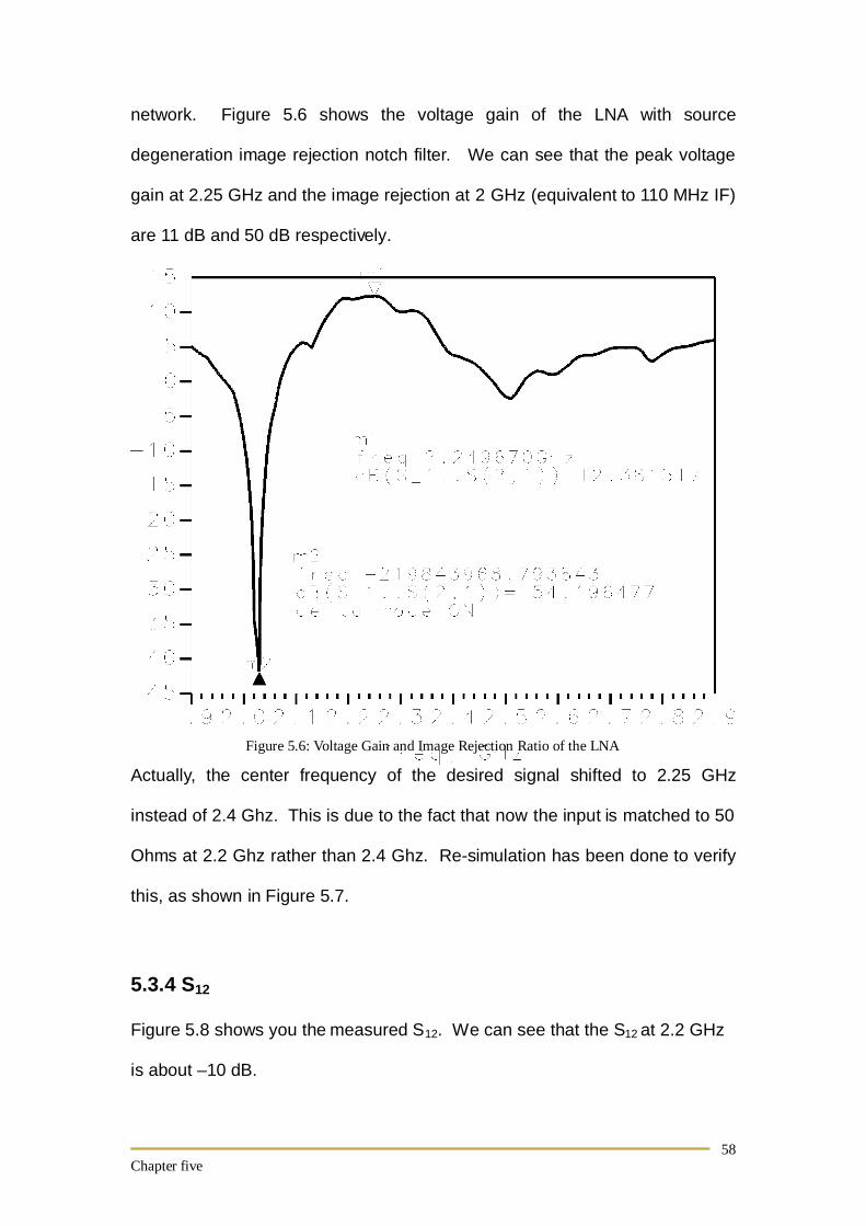
5.3.3 Frequency Response 57
5.3.4 S12 58
5.3.5 Noise Figure 60
5.3.6 Linearity (IIP3) 61
6 Design of Ultra Low Power Frontend Receiver
for Bluetooth System
6.1 Introduction 64
6.2 System Design 65
6.3 Circuit Design 66
6.3.1 LNA 66
6.3.2 Mixer 67
6.3.3 Polyphase filter 68
6.3.4 Antialiasing filter 69
6.4 Post simulation results 71
7 Conclusion 77

ix
List of Figure
Figure Description Page
Figure 1.1 Blocking Signals 5
Figure 2.1 Common source and common gate configurations 9
Figure 2.2 Complete schematic of LNA 10
Figure 2.3 Performance of single LNA versus device width 14
Figure 2.4 Series to parallel transformation 15
Figure 2.5 Output impedance of the LNA 17
Figure 2.6 Single-ended version Q-compensation circuit 17
Figure 2.7 Modified single-ended version Q-compensation circuit 19
Figure 2.8 Small signal model of Zin without neglecting Cgd 20
Figure 2.9 Circuit diagram of the SCA 23
Figure 2.10a SCA when switch is off 24
Figure 2.10b SCA when switch is on 24
Figure 2.11 Frequency response and Noise Figure of the first
stage LNA26
Figure 2.12 IIP3 of the LNA 27
Figure 3.1 Downconversion by Mixer 30
Figure 3.2a LNA with 2nd order notch filter 31
Figure 3.2b Impedance of notch filter and emitter of cascode BJT 31
Figure 3.3a LNA with 3rd order notch filter 32
Figure 3.3b Impedance of notch filter and source of cascode
CMOS32
Figure 3.4 Simplified amplifier circuit with source degeneration 34
Figure 3.5 Simplified amplifier circuit with source degeneration
and negative Gm cell34
Figure 3.6 Image Rejection Mixer 35
Figure 3.7 Complete schematic of the LNA with source
degeneration Image Rejection filter36
Figure 3.8 Frequency response and Noise Figure of LNA with
Image rejection filter38
Figure 3.9 S11 of the LNA 39

x
Figure 3.10 IIP3 for LNA with image rejection filter 40
Figure 4.1 CMOS on-chip inductor illustration 43
Figure 4.2 Inductor 45
Figure 4.3 Inductor model for on-chip inductor 46
Figure 4.4 Broken Guard Ring structure 46
Figure 4.5 SCA layout 47
Figure 4.6 Final layout of LNA with source degeneration image
rejection notch filter48
Figure 4.7 Frequency response and noise figure from the post
simulation of the whole LNA with source degeneration
image rejection notch filter
49
Figure 4.8 New S11 using L-type off chip matching network 50
Figure 4.9 Frequency response and noise figure with well-
matched S1151
Figure 4.10 Post simulated IIP3 at the LNA output 51
Figure 4.11 Post simulated IIP3 at the image rejection notch filter
output51
Figure 5.1 Chip Photo 55
Figure 5.2 Measured Q value of the on-chip inductor 56
Figure 5.3 Measurement setup for input matching 56
Figure 5.4 Measured input matching 57
Figure 5.5 Measurement setup for Frequency Response 56
Figure 5.6 Voltage Gain and Image Rejection Ratio of the LNA 58
Figure 5.7 Resimulation of Frequency response with improper
input matching59
Figure 5.8 Measured S12 59
Figure 5.9 Noise figure of the whole LNA with source
degeneration image rejection notch filter60
Figure 5.10 Measurement setup for IIP3 61
Figure 5.11 Captured frequency spectrum for two tone test 62
Figure 5.11 Interpolated IIP3 62
Figure 6.1 System block diagram for Bluetooth system 65
Figure 6.2 Schematic of LNA for Bluetooth system 66

xi
Figure 6.3 Mixer schematic for Bluetooth system 67
Figure 6.4 Polyphase filter schematic for Bluetooth system 68
Figure 6.5 Antialiasing fitler schematic for Bluetooth system 69
Figure 6.6 Layout of the Frontend for Bluetooth system 71
Figure 6.7 Frequency response and noise figure of the LNA 72
Figure 6.8 S11 of the LNA for Bluetooth system 73
Figure 6.9 Noise Figure of the Mixer 74
Figure 6.10 Frequency response and Noise Figure of the
Antialiasing filter75

xii
List of Table
Table Description Page
Table 1.1 Specification of general LNA 6
Table 1.2 Modified specification of LNA 6
Table 3.1 Performance summary of the LNA with image rejection
filter40
Table 4.1 Inductor parameters 45
Table 4.2 Summary of parameters from Sonnet, ASITIC and
FastHenry46
Table 4.3 Summary of post simulation performance 52
Table 5.1 Summary of performance of LNA with source
degeneration image rejection filter63
Table 6.1 Performance summary of each building block and
whole Frontend system76

Chapter one
1
Chapter 1
Introduction
1.1 Background
Wireless communication has been developing fast, especially in the last
decade. A mobile phone, due to its portability, mature technology and thus its
improved performance, shrinking size and reduced cost, is no longer a luxury.
It has already diffused to all level of working groups. As an example, in Hong
Kong, statistically, 1/3 of the population has at least one mobile phone. Such
a large market gives incentive to those who are in the wireless communication
field to research and further improve the performance and decrease the costs.
So, more and more people can afford it.
Nowadays, digital communication is the most favorite. It has many
advantages over analog communication in the past because of its high
performance like noise immunity, easy integration using inexpensive CMOS
technology. However, analog front-end IC is also an indispensable part in
mobile communication as it is the only intermediate stage of wireless
communication that convert digital signal to analog high frequency signal or
vice versa.
At present, GaAs and silicon bipolar and BiCMOS technologies constitute a
major section of the RF market. Because those technologies provide useful
features such as high breakdown voltage, high cutoff frequency, semi-

Chapter one
2
insulating substrate and high-quality inductors and capacitors. However, they
are still expensive when compared to CMOS technology. Also, using CMOS
can lead to a single chip solution in which RF front-end IC and digital
baseband system can be integrated together, and hence, greatly reduce the
cost. So, CMOS RF became an active research topic recently.
1.2 Challenges
Inspite of its attractions, there are still many difficulties that need to be
overcome for monolithic RF integration. The realization of some RF circuits in
CMOS like LNAs, power amplifiers, image-reject mixers, IF filter, voltage
control oscillators and frequency synthesizers has been demonstrated [1][2],
with comparable performances in terms of power consumption, linearity and
noise for those using GaAs and bipolar technology. Nevertheless, passive on-
chip elements like inductors and resistors have poor quality and suffer from
large process variation. Thus, some of the key components such as LNA,
image-reject filter, IF channel selection filters now used in the mobile phone
are still off-chip.
Among all these components, LNA is the most front-end building block in a
receiver. As termed Low Noise Amplifier, its main feature is low noise as
compared to other building blocks. This is because noise generated in the
LNA may amplify through the mixer, IF filter, VGA and ADC. Along this path,
the signal, as well as the noise may amplify by nearly 80dB-100dB. If the
front-end LNA noise is large, the system performance is greatly affected.
Even if a strong correction code is used in the baseband digital system, the
Chapter one
3
signal cannot be recovered.
Low supply voltage is another challenge. Differently from the digital system,
which do not consume so much power, the analog front-end IC burn a lot of
power. Thus, it is an advantage to decrease the supply voltage. On the other
hand, low supply voltage introduces more tough restrictions to the design of
analog front-end circuits, especially to the LNA and mixer. For LNA, low
supply voltage may degrade the noise performance, while the mixer, which in
general is designed with stacked transistors, may require some novel
techniques for low supply voltage.
Monolithic is the most challenging task in designing LNA. This is because
LNA extensively uses inductors and capacitors to provide bandpass functions.
However, as mentioned above, monolithic inductors suffer from low Q, which
may degrade the performance.
In this thesis, LNA with low supply voltage and image rejection using CMOS
technology will be explored. Q-enhancement technique will be used to
compensate for the low Q of inductors. Image rejection by source
degeneration is used to realize low supply voltage.
1.3 Thesis overview
The design of LNA and its analysis will be presented in chapter two, where the
topology, Q compensation technique and frequency tuning technique of LNA
will be given and followed by the analysis for the parameters like Gain, Noise,

Chapter one
4
Linearity and input matching.
Chapter three talks about the image rejection filter. Layout consideration
including inductor and Switchable capacitor array will be discussed in chapter
four. Measurements setup and results are presented in chapter five.
In chapter six, another project on ultra low voltage CMOS Frontend Receiver
for 2.4GHz Bluetooth system will be discussed. Finally a brief discussion and
conclusion will be drawn in chapter seven.
1.4 Specification
The design of LNA is based on the specification of the Bluetooth version 1.0B
[3]. Bluetooth is a new system for short distance or picocell wireless
applications that operates in the ISM (Industrial Scientific Medicine) band, that
is, the frequency band within 2400 – 2483.5 MHz. It can also be integrated
into most of the other standard systems to enhance the functionality.
To achieve the raw bit error rate (BER) of 0.1%, the actual sensitivity level of –
70dBm or better is required. Considering the minimum sensitivity level of –
70dBm, we can get the blocking signal levels for the bluetooth standard as
shown in figure 1.1.
In our architecture, we choose a single IF of 200MHz. Then we find that the
image frequency is located at 400MHz away from the wanted signal. With a
SNR of 22 dB so that provides less than 0.1% BER, the required image

Chapter one
5
rejection can be calculated –27dBm – (-70dBm) + 22dB = 81 dB. The choice
of SNR 22 dB is due to the fact that, typically, Bluetooth is used for indoor
application, where multipath fading channel is a significant factor that affects
the performance of the system. If in-phase (I) & quadrature—phase (Q)
channels are employed in the system, typically, the architecture can provide
about 35-40dB of image rejection. Thus, assuming the worse case of 30dB
image rejection offered by the I & Q channels architecture, the remaining 51
dB of image rejection is still required.
Noise in the system is another important factor that affects the whole system.
Given the minimum requirement of –70dBm sensitivity, we can find out that
the maximum noise figure (NF) is given by:
minmin, log10/174 SNRBNFHzdBmP Cin +++−=
dBNF 22≈
-10dBm
-27dBm
3GHz 2GHz
fc+3M
Hz
fc+2M
Hz
fc+3M
Hz
fc+2M
Hz
-70dBm
fc
2.4GHz 2.498GHz
-40dBm
-30dBm
Figure 1.1 Blocking signals
In-band

Chapter one
6
where –174dBm/Hz is the source resistance noise power of a 50Ohm system,
BC is the bandwidth, which is 1MHz for Bluetooth system, and SNR is
calculated according to the BFSK modulation with a given error rate of 0.1%
Since the above specifications are aimed to the system as a whole, the
specifications for LNA need some modification. From [4], requirement of LNA
is presented as shown in Table 1.1:
Parameters Requirements
Gain 15dB
Noise Figure (NF) 2dB
Linearity (IIP3) -10dBm
Input and Output return loss (S11) -15dB
Reverse Isolation (S21) -20dB
Table 1.1: Specification of general LNA
To meet the requirement of Bluetooth system and with some features added
to the LNA, some specifications are modified as shown in Table 1.2. For
example, due to high maximum allowable system noise figure of 23 dB, the
noise figure from the LNA can be higher to trade off the power consumption.
Parameters Requirements
Gain ~15-20dB
Noise Figure (NF) <6dB
Linearity (IIP3) >-10dBm
Image Rejection > 43dB
Table 1.2: Modified specification for LNA

Chapter one
7
Reference:
[1] A. Rofougaran, et al, “A single-Chip 900-MHz Spread-Spectrum Wireless Transceiver in 1-um CMOSPart II: Receiver Design,” IEEE J. Solid-State Circuits, pp. 535-547, April 1998
[2] D. K. Shaefer, et al, “A 115mW, 0.5um CMOS GPS Receiver with Wide Dynamic-Range Active Filters,” IEEE J. Solid-State Circuits, pp. 2219-2231, Dec. 1998
[3] Bluetooth Specification v1.0b [4] R. Razavi, “RF Microelectronics”, 1998

Chapter two
8
Chapter 2
Design of Low Noise Amplifier (LNA)
2.1 Introduction
In almost all wireless receivers, Low Noise Amplifier (LNA) is the most
challenging block. This is because we need the least number of elements to
achieve low noise, and however optimize most of the parameters
simultaneously. With the emphasis on using on-chip low-Q inductors,
designing LNA becomes stringent in terms of gain, noise and power
consumption. Besides LNA, image rejection filter for out of band image is
another important building block in a receiver. With the increasing demand for
monolithic integration, on-chip image rejection filter becomes indispensable
for system-on-a-chip.
As the process scales down, new design techniques have to be developed to
support low voltage design. Also, power consumption is another
consideration for portable device. In this chapter, we will explore and design
LNA that is suitable for low-voltage low-power application, together with the Q-
compensation circuit and frequency tuning circuit. Finally, Pre-simulation
results of the LNA will be presented.

Chapter two
9
2.2 Design of LNA
2.2.1 Topology of LNA
Basically, we can characterize LNA into two types: Common source or
common gate, as shown in Figure 2.1.
Both configurations have their advantages and disadvantages. For the
common gate configuration, its advantage is robust and easy to use.
However, in almost all cases, 50-Ohm matching is required for best
performance. One possible solution is to design the transconductance of the
device such that 501 =
mG, which means Gm = 20mS. Such a large Gm means
a higher power consumption is needed for a given process. The other method
is to use transformer as described in [1] to relax the Gm requirement.
However, such method is not easy to achieve with on-chip inductor for
standard CMOS processes, as its Q factor is not high enough.
On the other hand, given the same noise requirement, the common source
configuration can work with low Gm, which means lower power consumption,
as compared to common gate configuration. In addition, isolation is much
better for the common source one due to small parasitic capacitance Cgd.
Also, 50-Ohm real part can be achieved using inductive degeneration for the
RF input
RF input
Figure 2.1: Common source and common gate configurations
1/Gm

Chapter two
10
common source configuration due to the term gs
Sm
C
LG, where LS is the
inductance connected to the source and Cgs is the gate-source capacitance.
We can increase LS or decrease Cgs to get 50-Ohm real part without
increasing Gm. We will elaborate more on input matching later in this chapter.
Thus, common source configuration is chosen in our design with the
consideration of using on-chip inductor.
2.2.2 Design of LNA
Figure 2.2 shows the complete schematic of LNA.
As stated at the beginning, LNA should be kept as simple as possible to
minimize the noise figure. Actually, many recently reported LNA use cascode
configuration [2][3] for high gain without degradation of linearity and high
reverse isolation for a given power budget. However, under low supply
voltage, say 1 V, stacked transistor should be avoided to offer more headroom
and hence improve the linearity. Although the isolation is degraded. Some
use differential configuration for either its better common mode noise rejection
or linearity. On the other hand, power consumption has to be doubled for the
same noise figure. Thus, a single-ended, single device LNA is chosen.
….
Negative Gm cell
RF input
LNA output Lg
Ls
Lout
Figure 2.2: Complete schematic of LNA

Chapter two
11
Lg and Ls, together with Cgs of the NMOS form a 50-Ohm matching. Details of
input matching will be discussed further in this chapter. In our design, Lg is
supposed to be done off-chip. This is because, if it is totally done on-chip, the
thermal noise due to the low-Q inductor will be directly added to the total noise
without suppression. For example, in our case, the designed value is to be
12nH such that it matches at 2.4GHz. Further assume the Q of the on-chip
inductor is around 3. Then the series resistance of the on-chip inductor can
be found by 3.602
===Q
fL
Q
wLR gg
s
π. In a 50-Ohm system, the total noise
figure due to that resistance only is already 3.4dB. Also, if we consider the
final package, the LNA input has to be bonded out with wire, which can be
part of inductance. Thus, off-chip inductor is used for Lg.
On the other hand, on-chip Ls can be used, as the inductance is not large
enough to contribute much to the noise figure. Also, small inductance may
not degrade the total gain of LNA due to degeneration. However, since 50-
Ohm matching is done by gs
Sm
C
LG(suppose the imaginary part is zero at
2.4GHz), small Ls means small Cgs or large Gm to maintain a 50� real part.
So, next step is to design the NMOS transistor.
For Giga-hertz range operation, the transistor size has to be kept small such
that the transition frequency tω is high enough as compared to the desired
frequency. This can be easily explained as follows:

Chapter two
12
2
12
2
3
3
2
2
WLIC
WLCL
WIC
C
gw doxn
ox
doxn
gs
mt µ
µ
=≈=
So, in general, the minimum channel length is used with a large device width
to increase the transconductance and hence improve the noise figure while
keeping tω as high as possible. However, it has been proven that minimum
channel length will increase the total noise by 2~3 times due to the short
channel effect. One way to overcome this problem is to inject more current Id
into the device that the transconductance ( dm Ig α ) is large enough for low
noise. This is about trading off the power consumption for low noise. [4]
reported, for a given frequency, an optimized device width can be found with
the use of minimum channel length that can fulfill noise and power
consideration simultaneously, provided that the power is not extremely low.
Measured data shows a 3.4 dB noise figure with a power dissipation of 30mW
under a 1.5V supply.
However, with the emphasis on low power consumption, it is not suitable to
use the minimum channel length by increasing power dissipation for low
noise. As suggested in [5], 1.5~2 times of the minimum channel length can
be considered long channel, or the short channel effect is not severe enough
that it might not increase the noise by 2 to 3 times, without increasing the
power dissipation. In our case, 1.5 times the minimum channel length is used
(0.6um).
So far we always emphasize that the size of the transistor affects the

Chapter two
13
performance of LNA. However, what size of transistor can give the highest
performance? Optimization has been made for Noise Figure, IIP3 and Input
Reflection Coefficient (S11). Before figuring out the most optimized device
size, let us make some assumptions:
1. Fixed current of 1.2mA into the device: Such a power consumption is
low enough for the power budget
2. Fixed Voltage Gain (~20 dB)
3. Negative Gm circuit is removed so that the non-linearity effect is only due
to the input device only
4. As stated before, a constant channel length of 0.6�m is used to ignore
the noise due to short channel effect
5. For all cases of width, input is supposed to be matched and resonates at
2.4Ghz. To be consistent, Ls for input matching is kept the same for all
cases and Q of 3 is used. Lg is varied for the matching network to
resonate at 2.4Ghz and its Q is assumed to be 15
Figure 2.3 shows the simulated IIP3, Noise Figure and S11 versus the device
size.
As expected, increasing device size can help improved NF as the total
transconductance increases. On the other hand, IIP3 degrades with
increasing device width due to the increase of the aspect ratio.

Chapter two
14
Figure 2.3: Performance of single LNA versus device width
Thus, it can be easily found that the most optimized device width is
somewhere around 125um. The corresponding IIP 3, NF and S11 are 7.7 dBm,
1.82 dB and –30.5 dB respectively.
Another advantage of the above size is its Q in the matching network. For the
common source configuration, we can find that the Q of the input reactive
network is given by:
wCRQ
gss2
1=
where Rs is the source resistance and is equal to 50 ohm, Cgs is the gate-
source capacitance of the input device and ω is the frequency of interest.
Based on the size we have chosen, the Q value is 2.46. Such a low value
makes the circuit to less sensitive to parasitic.

Chapter two
15
Gain is another important parameter when designing LNA. Referring to
Figure 2.2, it can be easily found that the gain of the LNA is given by:
where gm is the transconductance of the MOS and Rout is the output
resistance looking into the output node of the LNA.
Suppose the output resistance due to NMOS is high enough that it can be
neglected, and the output LC tank is designed to resonate at 2.4 Ghz.
Remember with a low-Q on-chip inductor, the series resistance can be
transformed to parallel resistance as shown in Figure 2.4, the corresponding
parallel resistance Rp is given by )1( 2QQ
wLR out
p += , where Q is the quality
factor of the inductor Lout. Thus, (2.1) can be rewritten to:
Assume the Q is fixed, increasing Lout can improve the gain without burning
more power. However, increasing Lout means a smaller output capacitance
Cout parallel to the output inductor for resonance at desired frequency. In this
case, the center frequency may be highly sensitive to a small change of total
output capacitance. Nevertheless, a large Lout has an additional advantage
for the Q-compensation circuit, which will be discussed in the following
(2.1) sm
outmv Lsg
RgA
+=
1
Ls
Lp Rp
Rs =>
Figure 2.4: Series to parallel transformation
(2.2)
+
+= )1(
12Q
Q
wL
Lsg
gA out
sm
mv

Chapter two
16
section. Also, a frequency-tuning circuit can be added to deal with this
problem, as explained later.

Chapter two
17
2.2.3 Design of Q-compensation circuit
The main problem caused by the on-chip inductors is due to their low quality
factor. Due to process limitation, Q value below 10 is always the case.
Specifically, for digital CMOS process, its Q value can be low ranging from 2
to 4. Except for wideband application, this value is not adequate to provide a
narrow bandpass function. Let us consider the output impedance as shown in
Figure 2.5.
Suppose the LC tank (Cp and Lp) is designed to resonate at the desired
frequency. Due to low Q inductor, Rp becomes a finite value and thus cannot
make Zout to be infinity. As long as we can design a parallel component Zp
which is negative, then Rp and Zp can be cancelled out. This is the idea
behind the Q-compensation circuit.
Q-compensation circuit was first introduced in [6], the circuit schematic is
shown in Figure 2.6.
Figure 2.5: Output impedance of the LNA
Lp Rp Cp
Zout
Zp
Bias
Vdd Gp
Figure 2.6: Single-ended version Q-compensation circuit
A

Chapter two
18
The total transconductance looking into point A is given by:
where gm1 and gm2 are the transconductance of the cross-couple transistor.
To compensate for the low-Q inductor, we need to have p
pG
R1
= . As Rp
decreases, Gp has to be increased accordingly. This also explains why a
large inductance can benefit the Q-compensation circuit. This is because, as
Lout increases, Rp increase accordingly, and hence a lower Gp can be used.
Given the same power budget, lower Gp means a smaller device, that reduces
the parasitic capacitance and thus increases the tuning range capability,
lowers power consumption.
Assume gm2=Mgm1 where M is the constant multiplier, then (2.3) can be
reformed:
We can easily find that the most convenient value of M is as large as p ossible
such that M�M+1 and hence Gp = gm1. However, this leads to a very large
gm2, which is impractical for any process. In [6], M is set to 3 for enough Q-
compensation. On the other hand, due to large gm2 = 3gm1, the linearity
reported is –15 dBm while drawing 78mW under a 3V supply.
The low linearity is due to the unbalance transconductance between the
cross-couple transistors. One drain of a transistor is connected to the output
while the other is connected to the supply. Thus, a differential LNA using
(2.3) 21
21
mm
mmp gg
ggG
+−=
)1()1(1
1
21
M
Mg
gM
MgG m
m
mp +
−=+
−= (2.4)

Chapter two
19
differential Negative Gm cell is introduced in [7]. The same argument can be
adapted for our single-ended version. We can add a dummy component such
that the DC voltage point of the drain of both cross-couple transistors is the
same, as shown in Figure 2.7.
Now, the question is what kind of component should we choose: Resistor;
Inductor, or active device. Active device is obviously not a good choice as the
node voltage at point B becomes undefined. To solve this problem, a
common mode feedback circuit has to be added such that the node voltage
point A and B are the same, which is not good in terms of noise.
Resistor, on the other hand, seems to be a good choice. Nevertheless,
remember that the total required negative Gm is equal to the reciprocal of Rp,
where Rp is just a model due to the series resistance of the low-Q inductor.
Actually the node voltage A is defined by:
where Rs is the series resistance of the inductor as shown in Figure 2.4.
(2.5) makes it difficult to choose the value of the resistor. Value of Rp is
Bias
Vdd
Gp
Figure 2.7: Modified single-ended version Q-compensation circuit
A B
dsddA IRVV −= (2.5)

Chapter two
20
absolutely not suitable. This can be seen by modifying (2.5)
On the other hand, Rs is not suitable either. This is because the value of
p
pG
R1
= , Rp is the logical model of the inductor, not the real series resistance.
Without the series inductance, transformation cannot be made.
Thus, the best option is to use the same LC tank used for the output of the
LNA. In this case, we can have exactly the same characteristic on both sides
of the Negative Gm, like the differential one in [7][8]. The tradeoff here is a
larger area and a bit more noise due to the low-Q inductor. Nevertheless, we
can maintain the advantages of low power and high linearity.
Another feature offered by the Q-compensation circuit is its ability to tune the
input-matching network. To explain this feature, let us review how we derive
the input impedance using small signal model as shown in Figure 2.8.
Typically, we can get the input impedance Zin:
sgs
m
gssgin L
C
g
CLLjZ +−+≈ )
1(ω
dsddAdout
dddpddB IRVVIQQ
wLVIRVV −=≠+−=−= )1( 2
(2.6)
Cgd
Cgs
Lg
Ls
gmVgs
+ Vgs
- Zout
Zin
Figure 2.8: Small signal model of Zin without neglecting Cgd
(2.6)

Chapter two
21
Equation (2.6) is derived with the assumption that the gate-drain capacitance
Cgd is small enough that it can be ignored and Zout is infinity (or large enough),
and this is true in most cases. However, neglecting Cgd may lead to improper
input matching if Q-compensation circuit is added at the output of the LNA. To
see the effect, let’s re-derive the input impedance including Cgd and Zout.
To verify the correctness of (2.7), let’s make Cgd = 0, then equation (2.7) may
follow (2.6). Similarly, make Zout to be infinity, (2.7) converges to (2.6).
With the Q-compensation circuit added, Zout can now be varied. Consider the
X and 1+Y terms in (2.7) and rewrite it as shown in the next page, we can find
that the input impedance Zin becomes:
)'
')((
1)
1()(
A
CA
C
Lg
sB
CLLsZ
gs
sm
gssgin +++++=
(2.7)
outgsgdgsoutgdm
smgssgd
outgsgdgsoutgdmgs
gdsmgsggsgoutm
gs
sm
gssg
in
ZCsCCZCg
LsgCLsCY
ZCsCCZCgsC
CLsgCLsCLsZgX
YXY
XC
LgsC
sLsL
Z
+−++
=
+−++−
=
+
−+++=
)(
])1[(
])[(
])1)[((
bygiven are and where1
)1
(
2
22
(2.8)

Chapter two
22
Suppose the imaginary part is always designed to resonate at the desired
frequency, then we can see that: firstly, term A is a negative value as derived.
Thus, whenever (2.6) is used, the final value of the real part will be less than
the designed value. Secondly, the most important issue is the last term C’/A’.
Although it is always a real number, improper design of this term may lead to
a negative value. In this case, the real part of the input-matching network
becomes a negative value that indicates an undesired oscillation. Thus, Zout
becomes an important parameter to make sure that S11 will not be greater
than zero. Or, we can design Ls as small as possible to make sure that the
term C’/A’ is always greater than zero. Actually, this result agrees with [9], in
which the authors suggest to use a small source inductance during the design
{ }
{ }
'
'
1
1
0' and'
,0)('],)1[(' where
''''
)(
)(])1[(
)(
])1[(11
)( and
)(
)]1( where
)]1([)(
)]1([])1[()(
))(1(
)(
])1[(
)(
])1[(
2
2
2
222
2
222
2
22222
2222222
222
2
22
A
C
Y
ZCCDCZCgC
LgZCCBCCLsCCZgA
sDC
sBA
ZCsCCZCg
LgZCsCCCLsCCZg
ZCsCCZCg
LsgCLsCY
CsgC
gB
Csg
gCLsA
s
BA
sCLsCLggCsgsC
g
sCLsCLgCLgsgCLsCsgsC
g
Csg
sCgLsgCLs
sC
g
CsCgs
gLsgCLs
CCsCCgs
CgLsgCLsX
outgdgsgsoutgdm
smoutgsgdgdgssgsgdoutm
outgdgsgsoutgdm
smoutgsgdgdgssgsgdoutm
outgdgsgsoutgdm
smgssgd
gsmgs
m
gsm
mgss
gssgssmm
gsmgs
m
gssgssmgssmmgss
gsmgs
m
gsm
gsmsmgss
gs
m
gsgsm
msmgss
gsgsgdgdm
gdmsmgss
=+
=>
≈=−=≈+=+−+=
++=
+−+++−+
=
+−++
+=+
−=
−+−
=
+=
+−+−
=
+−+−+−
=
−−++
=
+++
=+
++=

Chapter two
23
of LNA.
2.2.4 Design of frequency tuning circuit
Process variation is one of the main problems for a circuit designer. This
problem becomes serious for narrow band application. Suppose an LC tank
is designed to resonance at frequency ω given by:
Take our case as an example, we have ω= 2.4GHz. And further suppose the
process variation is about +/-5%. The worse case variation of center
frequency is given by:
which corresponds to a frequency shift of around 100MHz. Various tuning
methods have been used [6][7][8]. Those methods make use of the Miller
effect to change the total output capacitance and hence provide tuning
capability. However, such method needs the device to be turned on, which
draws current, and at the same time, introduces noise to the LNA. Thus,
Switchable Capacitor Array (SCA) shown in Figure 2.9 is used.
Actually, the SCA is working in the digital domain. As the switch is turned on,
the drain of the switch is grounded. Thus, ideally, a single capacitor is seen at
the output. Since the transistor is blocked by the capacitor, no direct current
(2.9) LC
1=ω
ωω 976.0)05.1)(05.1(
1 ≈=CL
new (2.10)
Figure 2.9: Circuit diagram of the SCA
C0
Vb

Chapter two
24
can go through the transistor, that is, no power consumption. As the transistor
gm is zero, no noise is introduced by the SCA. However, it does have some
disadvantages for this design.
First of all, the transistor has its own “ON” resistance. The drain-source on
resistance is given by:
)( tgson VVW
LR
−α
Intuitively, increasing W can help minimize the resistance, and hence, the Q of
the capacitor. Nevertheless, as the size increases, the parasitic capacitance
increases accordingly. Such parasitic is the limitation of the tuning range. Let
us consider Figure 2.10.
Originally, we want a capacitance to be either zero or C0 when the transistor is
off and on respectively. However, due to the parasitic of the MOS as shown in
Figure 2.10a, the total capacitance at the output when the transistor is “off” is
given by:
010
10 CCC
CCC
P
Ptotal <
+=
When the transistor is “on”, the total output capacitance is C0. Thus, the total
capacitance change from “on” to “off” is no longer C0, but a value smaller than
C0. Thus, optimization has to be made to maximize the Q and tuning range at
C0
Vb
Figure 2.10a: SCA when switch is off
CP2
CP1 C0
Vb
Figure 2.10b: SCA when switch is on

Chapter two
25
the same time. Typically, a Q of 15~20 is enough to be neglected in terms of
the overall Q of the output of the LNA. This is because the low Q on-chip
inductor dominates the overall Q of the LNA. The layout technique is
important in designing SCA, which will be further discussed in Chapter four.
Chapter two
26
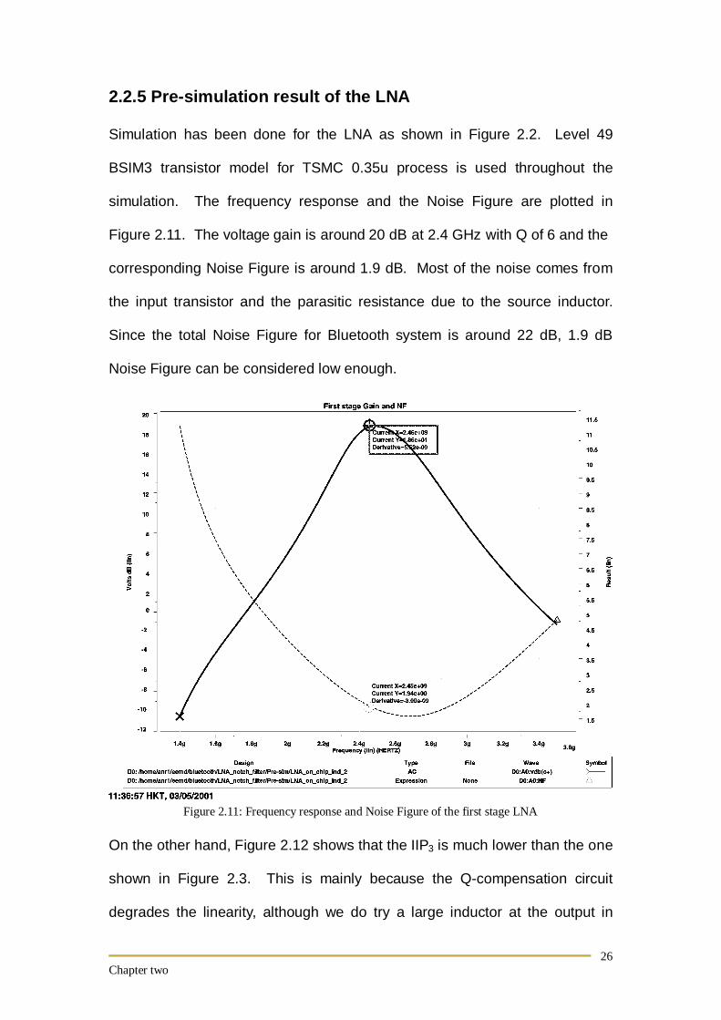
2.2.5 Pre-simulation result of the LNA
Simulation has been done for the LNA as shown in Figure 2.2. Level 49
BSIM3 transistor model for TSMC 0.35u process is used throughout the
simulation. The frequency response and the Noise Figure are plotted in
Figure 2.11. The voltage gain is around 20 dB at 2.4 GHz with Q of 6 and the
corresponding Noise Figure is around 1.9 dB. Most of the noise comes from
the input transistor and the parasitic resistance due to the source inductor.
Since the total Noise Figure for Bluetooth system is around 22 dB, 1.9 dB
Noise Figure can be considered low enough.
On the other hand, Figure 2.12 shows that the IIP3 is much lower than the one
shown in Figure 2.3. This is mainly because the Q-compensation circuit
degrades the linearity, although we do try a large inductor at the output in
Figure 2.11: Frequency response and Noise Figure of the first stage LNA

Chapter two
27
order to minimize the required -Gm, and hence obtain a smaller device size
and better linearity. Nevertheless, this value is still typical and acceptable in
most applications like Bluetooth.
Figure 2.12: IIP3 of the LNA

Chapter two
28
Reference:
[1] Hooman Darabi and Asad A. Abidi, “A 4.5mW 900-MHz CMOS Receiver for Wireless Paging,” IEEE Journal of Solid-State Circuits, vol. 35, No. 8, August 2000, pp 1085-1096.
[2] Brian A. Floyd, Jesal Mehta, Carlos Gamero, and Kenneth K.O, “A 900-MHz, 0.8-um CMOS Low Noise Amplifier with 1.2-dB Noise Figure,” IEEE Custom Integrated Circuits Conference, 1999
[3] Giovanni Girlando and Giuseppe Palmisano, “Noise Figure and Impedance Matching in RF Cascode Amplifiers,” IEEE Transactions on Circuits and Systems II: Analog and Digital Signal Processing, vol. 46, no. 11, November 1999
[4] Derek K. Shaeffer and Thomas H. Lee, “A 1.5-V 1.5-GHz CMOS Low Noise Amplifier,” IEEE Journal of Solid-State Circuits, vol. 32, No. 5, May 1997
[5] David A. Johns and Ken Martin, “Analog Integrated Circuit Design” [6] Chung Yu Wu and Shuo Yuan Hsiao, “The Design of a 3-V 900-MHz
CMOS Bandpass Amplifier,” IEEE Journal of Solid-State Circuits, vol. 32, No. 2, February 1997
[7] D. Leung and H. C. Luong, "A 3-V 45-mW CMOS Differential Bandpass Amplifier for GSM Receivers," Proceedings of IEEE International Symposium on Circuit and Systems 1998, Monterey, California, USA, pp. 341-344, June 1998
[8] D. Leung and H. C. Luong, "A Fourth-Order CMOS Bandpass Amplifier with High Linearity and High Image Rejection for GSM Receivers," Proceedings of IEEE International Symposium on Circuit and Systems 1999, Florida, USA, June 1999.

Chapter three
29
Chapter 3
Design of Image Rejection Notch Filter
3.1 Introduction
Except for Homodyne receivers, which use a zero IF, image is a serious
problem for a receiver. This is because undesired image signal may fall into
the desired signal band after frequency translation. Image can be considered
as in-band or out-of-band. For in-band image, rejection cannot be easily
made except the image-rejection mixer, which makes use of I and Q channels.
Theoretically, 100 percent of image rejection can be achieved. However, due
to device mismatch in the process, typical value of 30 dB is achieved, which is
not enough in most applications. Thus, many receiver architectures with out-
of-band image are chosen, which is always done using off-chip component
like SAW filter.
In this chapter, we are going to first talk about the basic image mechanism,
followed by the design of monolithic image rejection notch filter.

Chapter three
30
3.2 Image mechanism
In heterodyne receivers, signal band is translated to much lower frequencies
in order to relax the Q required for the IF filter. Frequency translation is done
by mixer as shown in figure 3.1.
The principle is based on the mathematical expression as follows: Consider a
signal of frequency ωRF with amplitude ARF and the LO frequency of ωLO with
amplitude ALO, and lower side band is chosen, then we can see that:
[ ]twwtwwAA
twAtwA LORFLORFLORF
LOLORFRF )sin()sin(2
)sin()sin( ++−=•
Thus, after translation, we can get a signal with lower frequency ωIF=ωRF-LO.
However, it can also be proven that, with an unwanted RF signal at frequency
ωRF-2ωIF, this signal will be downconverted to ωIF with the same mixer. This is
what we call image frequency. To prevent the unwanted image signal to be
down-converted to the same IF as the desired signal, image reject off-chip
SAW filter is commonly inserted between the LNA and mixer. Nevertheless,
such an off-chip component requires 50 Ohm matching. Also, most of the
time, this SAW filter is made of passive elements, that is, an insertion loss is
introduced in the signal path.
� �RF
� �LO
� �IF
Figure 3.1: downconversion by mixer

Chapter three
31
3.3 Design of Monolithic Image Rejection Filter
3.3.1 Past development
Not many published paper investigated on monolithic image rejection filter
until few years before. On-chip image rejection filter was first introduced
[1][2][3]. The idea is explained as follows:
Consider Figure 3.2a, by designing the impedance Z1 and Z2 as shown in
Figure 3.2b, the image signal can be ‘steered’ away from the signal path to
ground through the image rejection notch filter, but not the desired signal.
The reported image rejection can be greater than 50 dB when using on-chip
inductors with Q value of 7 in BJT technology. If a 2nd order notch filter is
used, the IF cannot be low, or otherwise, Z2 becomes less than Z1, which
‘steer’ away the desired signal. Thus, a 300 MHz IF is chosen. Such a high
IF may introduce difficulty to the Analog-to-Digital converter, or a double IF
receiver architecture has to be used. Finally, as there is no control of the
desired frequency in the notch filter and the notch filter is connected to the
signal path, the linearity is always degraded. The reported IIP 3 is around –28
dBm with a gain of 28 dB.
Notch filter
Z1
Z2 Vi
Vo
Figure 3.2a: LNA with 2nd order notch filter
Z
Z1
Z2
fimage fwanted
Figure 3.2b: Impedance of notch filter and emitter of cascode BJT

Chapter three
32
Another design of image rejection filter is introduced [4] in CMOS technology
as shown in Figure 3.3a.
Basically, the idea is the same as in [1] except a blocking capacitor is added
to form a third order notch filter. This added blocking capacitor provides
another control of the wanted signal so that Z2 is always greater than Z1 at the
desired signal. The reported IIP3 is –2 dBm with a gain of 18 dB with an on-
chip inductor Q value of 5 in 0.25um CMOS technology. Nevertheless, in
most cases, the transconductance of the cascode is high for high gain and low
noise, which means a small Z1. Thus, the difference between Z1 and Z2
cannot be high, and hence, the image rejection. The reported image rejection
is around 12 dB.
Another improved version is reported in [5], in which the notch filter is moved
to the second stage bandpass filter. Since the transconductance of the
second stage bandpass filter is comparatively lower than the first stage, a
higher image rejection can be achieved. The reported image rejection can be
greater than 60 dB, which is much higher than in [4].
Z1
Z2
Figure 3.3a: LNA with 3rd order notch filter
Notch filter
Z
Z1
Z2
fimage fwanted
Figure 3.3b: Impedance of notch filter and source of cascode CMOS

Chapter three
33
For the previous designs [1][2][3][4], the image rejection notch filter is inserted
into the cascode LNA. In the receiver path, this means the LNA is combined
with the image rejection filter into one building block. However, with this
combination, the noise due to the image rejection filter cannot be suppressed
by the high gain LNA because of the cascode configuration, the gain is only 1
from the node between the input device and the cascode device. So, noise
from the notch filter cannot be suppressed. Thus, in the designs discussed
above, the Noise Figure cannot be lower than 4.5 dB with relative high power
consumption.
In [5], the image rejection and the Noise Figure can be improved by
introducing one more stage between the LNA and Mixer. However, in terms of
system consideration, we want to reduce the number of building blocks in the
receiver path as much as possible for higher linearity and low noise.
One of the common problems in all previous designs is the use of cascode
configuration. As discussed in Chapter 2, under a low supply voltage,
cascode configuration should be avoided in all sense.

Chapter three
34
3.3.2 Proposed Image rejection notch filter [6]
Consider the schematic in Figure 3.4. This is the most basic amplifier with
source degeneration, for which the gain is given by:
Normally, the function of ZS is to improve the linearity by trading off the gain.
Here, we propose to use a second-order LC tank to design ZS so that it
resonates at the image frequency. As a result, the gain at the image
frequency decreases close to zero, and a notch filter is achieved.
Several advantages are offered by this design:
1. Only one transistor is involved to provide image rejection that can support
low voltage design, as compared to [1][2][3][4].
2. The non-linearity effect due to the Q-compensation circuit would not be
affected if it is added to the source of the transistor to compensate the
Figure 3.4: Simplified amplifier circuit with source degeneration
Vdd
Vout Vin
ZO
ZS
(3.1) Sm
OmV Zg
ZgA
+=
1
Figure 3.5. Simplified amplifier circuit with source degeneration and negative Gm cell
Vdd
Vout Vin
ZO
ZS
Negative Gm

Chapter three
35
low Q inductor, as shown in Figure 3.5. This is because the output is
taken at the drain of the transistor, not the source. Thus, even the poor
linearity of the Q-compensation circuit, it does not affect the signal path.
3. This simple structure can be combined with most of the circuit. For
example, the source degeneration image rejection filter can be combined
with the single-balanced mixer or Gilbert mixer to form an image rejection
mixer. Figure 3.6 shows the schematic of the image rejection mixer using
Single-balanced mixer.
In terms of system design, we are trying to combine the image rejection
filter and mixer to form one building block instead of combining the LNA
with the image rejection notch filter.
4. Since the image rejection filter is moved behind the LNA (as shown in
Figure 3.7 in the next section), the noise due to the image rejection filter
can be suppressed by high gain LNA, as compared to [1][2][3][4].
Of course, there are some other disadvantages. First, as the IF becomes
lower, the gain decreases at the desired signal according to equation 3.1.
LO+ LO-
RF Source degeneration Image Rejection filter
Figure 3.6: Image Rejection mixer

Chapter three
36
Also, it can provide a narrow band function.
3.3.3 Complete design of LNA with source degeneration Image
Rejection filter
Figure 3.7 shows the complete schematic of the LNA with source
degeneration Image rejection filter. The LNA is the common mode
configuration as discussed in Chapter 2. The gate inductor is chosen off-chip
for lower noise figure.
A PMOS second stage input is chosen. This is because a NMOS Q-
compensation circuit as shown in Chpater 2 can be used. Remember the
mobility of NMOS is about 2 to 3 times larger than PMOS. If we use a NMOS
second stage input and a PMOS Q-compensation circuit, the device of the
PMOS has to be large, or larger power consumption is needed. Also, the
parasitic capacitance would increase accordingly which decreases the
….
On-Chip
Vdd
Lg
LS
LO
RFout
RFin
Negative Gm Negative
Gm
Rout
Figure 3.7: Complete schematic of the LNA with source degeneration Image Rejection filter
Biasn
Biasn

Chapter three
37
available frequency tuning range.
Since PMOS is intrinsically low noise, the noise figure due to the second
stage input device would be small. The only disadvantage is that a blocking
capacitor and a biasing resistor are needed. The biasing resistor should be
theoretically large enough to reduce its current noise. By rule of thumb, two
thousand to four thousand ohms is enough for low noise [7]. The on-chip
blocking capacitor is designed such that its impedance is not high at the
desired frequency. Thus, the capacitance has to be high. On the other hand,
its parasitic capacitance would be high also. Optimization is made here such
that the impedance and the parasitic capacitance due to the blocking
capacitor are low and in our case the capacitance is about 1.8pF.
As discussed in Chapter 2, frequency-tuning circuit is necessary to cope with
the process variation. Thus, a SCA is added at the image rejection filter.
Different IF can be used by this SCA. On the other hand, SCA is not added at
the output of the first stage as it can be tuned by proper input matching
network.
For simplicity, an open pad is used for the output of the LNA output for 50
Ohm matching. Thus, the second stage forms an image rejection buffer. The
use of 50Ohm resistor for matching degrades the gain from the first stage
LNA and increases the noise figure. However, as our purpose is to
demonstrate our idea of source degeneration image rejection filter, we can
scale the gain during measurement.

Chapter three
38
3.3.4 Pre-simulation of the complete LNA with source
degeneration Image Rejection filter
Figure 3.8 shows the frequency response and Noise figure of the LNA with
source degeneration image rejection filter. The voltage gain of the first stage
output is plotted for comparison. We can see there is a notch at the IF
frequency (~200Mhz). On the other hand, due to the suppression of the gain
at the image frequency, the noise increases. The total image rejection can be
greater than 50 dB with respect to the desired frequency, and it can be further
improved with the Q of the inductor.
On the other hand, the Noise Figure drops to around 3.8 dB. This is because
a 50 Ohm resistor is used for matching. Thus, Figure 3.8 shows a drop in the
gain at the second stage output and also the inductive degnerative at the
1st stage gain
2nd stage gain
Noise Figure
Figure 3.8: Frequency response and Noise Figure of LNA with image rejection filter

Chapter three
39
source. If we design a resistor such that the voltage gain at the desired
frequency is the same as the first stage output, the Noise Figure is actually
2.7 dB.
As discussed in Chapter 2, the Q compensation circuit can affect the input
matching (S11). Figure 3.9 presents S11 versus frequency.
Figure 3.9: S11 of the LNA
The minimum S11 is around –10dB at 2.45 GHz. This is not a low value
compared to typical published papers, although it is still acceptable in most
applications such as Bluetooth.

Chapter three
40
To prove whether the Q-compensation circuit for the source degeneration
image rejection filter will affect the linearity or not, simulation has been done
by inputting two tones at 3 Mhz apart. The IIP3 for both the first stage LNA
output and the second stage image rejection filter output is plotted in Figure
3.10.
As compared to Figure 2.12, the IIP3 is almost the same.
Table 3.1 shows the Pre-simulation result of the LNA with source
degeneration image rejection filter:
Parameters Pre-simulation result Voltage Gain 21 dB
Image Rejection ratio > 50 dB Noise Figure 3.3 dB
Power dissipation 3.5 mW S11 -10 dB IIP3 -7 dBm
Supply voltage 1 V Table 3.1: Performance summary of the LNA with image rejection filter
Figure 3.10: IIP3 for LNA with image rejection filter

Chapter three
41
Reference:
[1] Jose Macdeo, Miles Copeland and Peter Schvan, “A 2.5GHz Monolithic Silicon Image Reject Filter,” IEEE Custom Integrated Circuits Conference, 1996
[2] Jose Macdeo, Miles Copeland and Peter Schvan, “A 1.9 GHz Silicon Receiver with On-chip Image Filtering,” IEEE Custom Integrated Circuits Conference, 1997
[3] Jose Macdeo, Miles Copeland and Peter Schvan, “A 1.9 GHz Silicon Receiver with On-chip Image Filtering,” IEEE Journal of Solid-State Circuits, Vol. 33, No. 3, March 1998
[4] Hirad Samavati, Hamid R. Rategh and Thomas H. Lee, “A 12.4mW CMOS Front-End for a 5 GHz Wireles-LAN Receiver,” Symposium on VLSI, 1999
[5] C. B. Guo, A. Chan, and H. C. Luong, "A 2-V 950-MHz LNA with Notch Filter for Wireless Receivers," IEEE Radio-Frequency Integrated-Circuit Symposium, 2001 (RFIC), Arizona, USA, May 2001, to appear
[6] A. Chan, C. B. Guo, and H. C. Luong, "A 1-V 2.4-GHz CMOS LNA with Source Degeneration as Image-Rejection Notch Filter for Bluetooth Applications," IEEE International Symposium on Circuits and Systems 2001, Sydney, Australia, May 2001, to appear
[7] Thomas Lee, “The Design of CMOS Radio-Frequency Integrated Circuits”

Chapter four
42
Chapter 4
Layout consideration
4.1 Introduction
How high the performance of the circuit, especially for RF circuits, depends
heavily on the circuit layout. Common centroid and fingering are common
techniques for the transistor layout. In this chapter, however, we are going to
focus on the design of on-chip inductors and Switchable Capacitor Array
(SCA) as they play an important role in LNA design as mentioned in the
previous chapter. Final floorplan and layout of the complete LNA with image
rejection filter will be given. Finally, Post-simulation with the final layout will be
presented.

Chapter four
43
4.2 On-chip Inductor Design
On-chip inductor is a very process-dependent passive device. Recently,
many published papers discussed many techniques to improve the Q of on-
chip inductor such as circular spiral inductor, double metal and multi-metal
[1][2], guard ring, taper inductor [4] and patterned ground shielding [5].
However, all these techniques have their limitation in terms of the use of
process. To explain these, let us discuss further how the geometry of an on-
chip inductor affects the Q. Consider Figure 4.1
The Q can be affected by three mechanisms: Metal loss, Substrate loss and
eddy current loss. The metal loss is due to the physical resistance in the
metal. Increasing of metal width can remedy this problem. However, it
increases the parasitic capacitance (Cp) between the metal and the substrate,
which increases the substrate loss as high frequency can easily leak to the
substrate through Cp. Eddy current loss is due to the image current formed in
the substrate that opposes the magnetic field from the inductor itself. Due to
Substrate
Cp
metal
Magnetic field
Figure 4.1: CMOS on-chip inductor illustration

Chapter four
44
the above limitation, typically, the values of on-chip inductors range from 2nH
to 10nH.
Multilevel connection of metal layers is proved to improve the Q without
special process [2][3]. However, as the operating frequency increases, the
loss becomes higher as the parasitic capacitance increases, which may lead
to higher substrate loss.
Patterned ground shield is another technique to improve the quality factor by
around 1.5 times [5]. However, this technique is useful only for a lightly doped
substrate, although it doesn’t deviate from the standard CMOS process.
Nevertheless, to emphasize the possibility of combining analog receiver with
the digital baseband processing part, substrate of CMOS processes are
generally highly doped to prevent latch up.
It has been proved that circular inductor can improve the quality factor of on-
chip inductor. However, layout of a circular shape is not an easy task. Also,
as discussed with Dr. Ali M. Nilnejad (Author of ASITIC), such improvement is
on average about 5 -10%, of which some portions are contributed by noise. At
the same time, given the same inductance, the area of a circular inductor has
to be larger than the square one, thus, leading to a higher substrate loss.
For Giga-hertz application, eddy current loss is not the main factor of low Q
on-chip inductor. Thus, care is taken in handling the resistance on the metal
loss and the substrate loss. To reduce the substrate loss, the total metal area

Chapter four
45
should be kept as small as possible. On the other hand, smaller area means
a higher sheet resistance, as the metal width has to be small to keep the
same inductance. Thus, optimization point can be found such that the total
loss is minimized [6][7][8] by sweeping a wide range of inductor length, width
and number of turns.
Several simulation tools of inducotor: ASITIC [9], Sonnet [10] and FastHenry
[11] are used for comparison. Sonnet gives a full 3D simulation of inductor
and thus provides very accurate result. However, the simulation time increase
exponentially with the size of the inductor. For a circular inductor, it may take
a lifetime to get the result. ASITIC and FastHenry provide a pseudo 3D
simulation of the inductor, and they take much less time to get the result. In
our case, a square inductor is designed and simulated in the above three
simulation tools. We choose a square inductor because we can use Sonnet
for higher accuracy. Also, eddy current loss can be taken into account in
ASITIC for a square inductor (eddy current simulation cannot be applied to
inductor with shape other than square). Figure 4.2 shows the layout of the
inductor and Table 4.1 summarizes the geometry of the inductor.
Parameters ValuesWidth 12 um
Spacing 1.2 umTurns 5
Metal Top metalInner dim 60 um
Figure 4.2: Inductor Table 4.1: Inductor
parameters

Chapter four
46
Figure 4.3 shows the inductor model. Rs models the sheet resistance. Cp and
Rp model the substrate loss and the eddy current loss. Table 4.2 shows the
parameters from the above three simulation tools.
Tools Ls Rs C1p R1p C2p R2p
Sonnet 3.81nH 13.8 0.11pF N/A 0.12pF N/A
ASITIC 3.8nH 16.5 0.1pF 54 0.102pF 76.8
FastHenry 3.9nH 13 N/A N/A N/A N/A
Table 4.2: Summary of parameters from Sonnet, ASITIC and FastHenry
Coupling throught substrate is another problem for monolithic design [12].
Induced current in the substrate can go to another circuit easily because of
the low resistivity substrate.
Guard ring is used to solve this problem. Many guard ring structures have
been studied. Here we adopted the broken guard ring [13], as shown in
Figure 4.4. The advantage of this structure is that it can improve the substrate
noise coupling without much effect on the inductance. It can also prevent an
eddy current formed in the broken guard ring.
Ls Rs
R1p
C1p
R2p
C2p
Figure 4.3: Inductor model for on-chip inductor
Broken guard ring
Inductor
Figure 4.4 Broken Guard Ring structure

Chapter four
47
4.3 Switchable Capacitor Array (SCA)
As discussed in chapter two, SCA has many advantages over other frequency
tuning techniques like Miller Capacitance or varactor. However, care must be
taken in the layout so that SCA has the best performance. To minimize the
parasitic capacitance, we have to keep the drain area as small as possible to
maximize the tuning range. On the other hand, the aspect ratio has to be kept
as large as possible to improve the Q value of the SCA. Thus, a donut cell is
used as the transistor layout. Figure 4.5 shows the layout of a one-bit SCA.
Figure 4.5: SCA layout
One Donut Cell
Chapter four
48
4.4 Final Layout and Post Simulation result
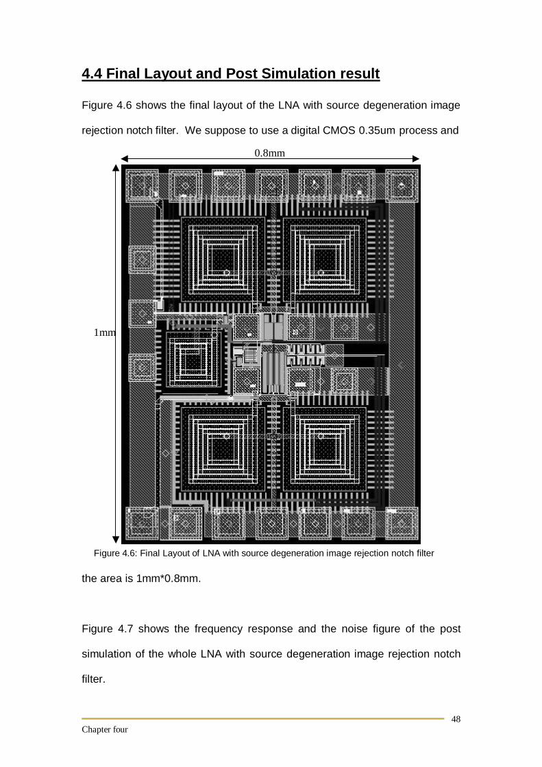
Figure 4.6 shows the final layout of the LNA with source degeneration image
rejection notch filter. We suppose to use a digital CMOS 0.35um process and
the area is 1mm*0.8mm.
Figure 4.7 shows the frequency response and the noise figure of the post
simulation of the whole LNA with source degeneration image rejection notch
filter.
Figure 4.6: Final Layout of LNA with source degeneration image rejection notch filter
0.8mm
1mm

Chapter four
49
Figuree 4.7 shows similar performance as in the pre-simulation results as
shown in chapter three. However, due to the parasitic from the layout, S11 is
further degraded. So, an simple L -type off-chip matching network is designed
by adding an extra capacitor of 2p connected to the gate inductor input and
the ground. Figure 4.8 shows the new S11. Since, the matching network is
changed, the final frequency response has also been changed, as shown in
Figure 4.9. The peak voltage gain is shifted to a lower frequency. However,
the gain at 2.45GHz is still around 20 dB. Because the input matching is well-
matched, the minimum achievable noise figure of around 3 dB is possible.
Figure 4.7: Frequency response and noise figure from the post simulation of the whole LNA with source degeneration image rejection notch filter
1st stage gain
2nd stage gain
Noise Figure

Chapter four
50
Figure 4.8: New S11 using L-type off chip matching network
Figure 4.9: Frequency response and Noise Figure with well-matched S11

Chapter four
51
Figure 4.10 and 4.11 shows the post-simulated IIP3 at the first stage LNA
output and the second stage image rejection notch filter. Once again, we can
see that linearity is nearly the same as the IIP3 at the first stage LNA output.
Figure 4.10: Post simulated IIP3 of the LNA output
Figure 4.11: Post simulated IIP3 at the image rejection notch filter output
Chapter four
52
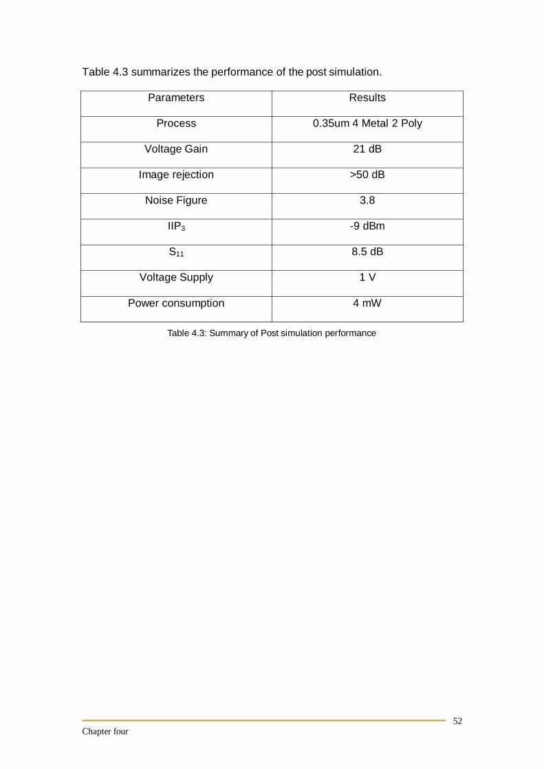
Table 4.3 summarizes the performance of the post simulation.
Parameters Results
Process 0.35um 4 Metal 2 Poly
Voltage Gain 21 dB
Image rejection >50 dB
Noise Figure 3.8
IIP3 -9 dBm
S11 8.5 dB
Voltage Supply 1 V
Power consumption 4 mW
Table 4.3: Summary of Post simulation performance

Chapter four
53
Reference:
[1] Min Park, et al, “High Q CMOS-compatible Microwave Inductors Using Double-Metal Interconnection Silicon Technology,” IEEE Microwave and Guided Wave Letters, Vol. 7, No. 2, Feb 1997
[2] Joachim N. Burghartz, et al., “Microwave Inductors and Capacitors in Standard Multilevel Interconnect Silicon Technology,” IEEE Transcations on Microwave Theory and Techniques, Vol. 44, No. 1, Jan 1996
[3] J. E. Post, “Optimizing the design of Spiral Inductors on Silicon,” IEEE Transcations on Circuits and Systems II: Analog and digital Signal Processing, vol 47, No. 1, Jan 2000
[4] Derek K. Shaeffer and Thomas H. Lee, “A 1.5-V 1.5-GHz CMOS Low Noise Amplifier,” IEEE Journal of Solid-State Circuits, vol. 32, No. 5, May 1997
[5] C. Patrick Yue, et al., “On-Chip Spiral Inductors with Patterned Ground Shields for Si-Based RF IC’s,” IEEE Journal of Solid-State Circuits, Vol. 33, No. 5, May 1998
[6] John R. Long and Miles A. Copeland, “The Modeling, Characterization, and Design of Monolithic Inductors for Silicon RF IC’s,” IEEE Journal of Solid State Circuits, Vol. 32, No. 3, Mar 1997
[7] Joachim N. Burghartz, et al, “RF Circuit Design Aspects of Spiral Inductors on Silicon,” IEEE Journal of Solid-State Circuits, Vol. 33, No. 12, Dec 1998
[8] J.E. Post, “Optimizing the Design of Spiral Inductors on Silicon,” IEEE Transcations on Circuits and Systems II: Analog and Digital Signal Processing, Vol. 47, No. 1, Jan 2000
[9] Ali M. Nilnejad and robber G. Meyer, “Analysis, Design and Optimization of Spiral Inductors and Transformers for Si RF IC’s,” IEEE Journal of Solid-State Circuits, Vol. 33, No. 10, Oct 1998
[10] Sonnet Manual [11] FastHenry Manual [12] Joachim N. Burghartz, “Progress in RF Inductors on Silicon –
Undersanding Substrate Losses,” IEEE IEDM, pp 523-526, 1998 [13] Alan L. L. Pun, et al, “Substrate Noise Coupling Through Planar Spiral
Inductor,” IEEE Journal of Solid-State Circuits, Vol. 33, No. 6, Jun 1998

Chapter five
54
Chapter 5
Measurement Result
5.1 Introduction
In this chapter, measurements result such as Gain, Input matching, Noise
figure and linearity will be presented. Measurements setup will be illustrated.
Finally, a summary of the measurement result will be tabulated together with
the past work.
Chapter five
55
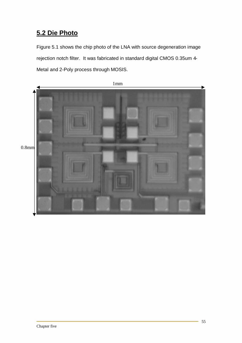
5.2 Die Photo
Figure 5.1 shows the chip photo of the LNA with source degeneration image
rejection notch filter. It was fabricated in standard digital CMOS 0.35um 4-
Metal and 2-Poly process through MOSIS.
1mm
0.8mm

Chapter five
56
5.3 Measurement
5.3.1 On-chip Inductor
Figure 5.2 shows the inductance and the Q value of the on-chip inductor. We can see
that the measured inductor Q is very close to the simulated Q in ASITIC.
5.3.2 Input matching (S11)
Figure 5.3 shows measurement setup of the input matching. Calibration is
made up to point A. The transmission line is designed to match at 2.4Ghz.
A DUT
Transmission Line Bondwire
HP 8753D
Figure 5.3: Measurement setup for Input matching
B
Figure 5.2: Measured Q value of the on-chip inductor
Chapter five
57
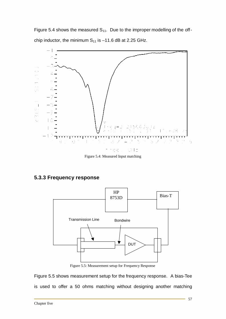
Figure 5.4 shows the measured S11. Due to the improper modelling of the off -
chip inductor, the minimum S11 is –11.6 dB at 2.25 GHz.
5.3.3 Frequency response
Figure 5.5 shows measurement setup for the frequency response. A bias-Tee
is used to offer a 50 ohms matching without designing another matching
DUT
Transmission Line Bondwire
HP 8753D
Figure 5.5: Measurement setup for Frequency Response
Bias-T
Figure 5.4: Measured Input matching
Chapter five
58
network. Figure 5.6 shows the voltage gain of the LNA with source
degeneration image rejection notch filter. We can see that the peak voltage
gain at 2.25 GHz and the image rejection at 2 GHz (equivalent to 110 MHz IF)
are 11 dB and 50 dB respectively.
Actually, the center frequency of the desired signal shifted to 2.25 GHz
instead of 2.4 Ghz. This is due to the fact that now the input is matched to 50
Ohms at 2.2 Ghz rather than 2.4 Ghz. Re-simulation has been done to verify
this, as shown in Figure 5.7.
5.3.4 S12
Figure 5.8 shows you the measured S12. We can see that the S12 at 2.2 GHz
is about –10 dB.
Figure 5.6: Voltage Gain and Image Rejection Ratio of the LNA

Chapter five
59
Figure 5.7: Resimulation of Frequency response with improper input matching
Figure 5.8: Measured S12

Chapter five
60
5.3.5 Noise Figure
Basically, the measurement setup as shown in figure 5.5 can be used again
except that the measurement equipment is now replaced by Agilent N8975A.
Figure 5.9 on the previous page shows the measured noise figure.
As predicted from simulation in chapter three, the noise figure is very high at
the image frequency. On the other hand, the noise figure at 2.25Ghz is
around 5.1 dB.
Figure 5.9: Noise Figure of the LNA with source degeneration image rejection notch filter

Chapter five
61
5.3.6 Linearity (IIP3)
Figure 5.10 illustrates the measurement setup for the linearity. Two signal
generators are used to generate two pure sine tones with 3MHz seperation.
High impedance probe is also used to probe the output signal of the LNA
output. Figure 5.11 shows the captured frequency spectrum with two tone test
applied together with the intermodulation frequency and Figure 5.12 shows
the frequency spectrum with two input sine waves and their intermodulation
product.
DUT
Transmission Line Bondwire
Combiner H-183-4
Figure 5.10: Measurement setup for IIP3
Bias-T Spectrum Analyser Agilent E4404B
Agilent E4433B
HP 8648C

Chapter five
62
Figure 5.11: Captured frequency spectrum for two tone test
Figure 5.12: Interpolated IIP3

Chapter five
63
To measure the IIP3, an increasing input power is applied to get the
corresponding output voltage. Figure 5.11 shows the interpolated IIP3 of the
output of the image rejection notch filter. From the figure, the IIP3 is much
higher than the simulated result. This is because the gain for the LNA is
about 12 dB. Here we try to improve the linearity by trading off the gain. The
main reason is that the linearity requirement for bluetooth has to be larger
than –16 dBm, which is the most tough requirement.
Table 5.1 summarizes the overall performance of the LNA with source
degenration image rejection notch filter as well as the performance for the
existing design refered in chapter 3 for comparison.
[3] [4] [5] This work
Process BJT 0.25um CMOS 0.5u CMOS 0.35u CMOS
IF 300 MHz 300 MHz 70 MHz 110 MHz
Gain 28 dB 18 dB 22 dB 12 dB
NF 4.8 dB 3.8 dB 10 dB 5.1 dB
IIP3 -28 dBm -2 dBm -18 dBm 1 dBm
IR > 60 dB 20 dB > 50 dB > 50 dB
Supply voltage 2.7 V 2 V 2 V 1 V
Power 33 mW 12 mW 22 mW 3.6 mW
Table 5.1: Summary of performance of LNA with source degeneration image rejection filter

Chapter six
64
Chapter 6
Design of Ultra Low Power Frontend
Receiver for Bluetooth System
6.1 Introduction
Bluetooth is a newly developed system that is used for short distance wireless
communication. Because of its simplicity, it is supposed to be able to plug into
many existing wireless systems or even home accessories to form a small
wireless network.
From the previous chapter, we know that 1-V LNA is possible without
degradation of the performance. In this chap ter, we are going to demonstrate
the possibility of a single 1-V supply receiver with ultra low power
consumption. At the time the writer finishes this thesis, the chip is still being
fabricated. Thus, only simulation results are provided.

Chapter six
65
6.2 System Design
Figure 6.1 shows the system block diagram of the bluetooth receiver
After the RF signal goes into the antenna and is being amplified by LNA, it is
down converted to an IF of 1 MHz. Such a low IF can relax the power
consumption in the IF Filter and the SDADC. To further reduce the power
dissipation, all inductors are off-chip. This can also improve the total noise
figure, although it is not a main concern in Bluetooth system. Since the image
signal is located in-band, an image rejection mixer using I and Q channels is
used. Because the minimum in-band image rejection requirement is 20 db,
such image rejection architecture is adequate even if the mismatch of the
device is about 5 percents [1]. To eliminate the possible off-chip inductor
mismatch, we try to minimize the number of off-chip inductors. Hence, a
simple VCO is used instead of cross-coupled IQ VCO. This can also reduce
the power consumption. On the other hand, generation of IQ LO signal is
done by using Polyphase filter. To make the image rejection immune from
further mismatch, a two-stage Polyphase filter is adopted [1]. Antialiasing
filters are added between the mixer and the IF filter since switched-capacitor
2 stage
Polyphas
IF Filter SDADC Baseband
data
2.4 Ghz RF
1 MHz IF
Alan
Joseph
Vincent
Figure 6.1: System Block diagram for Bluetooth system
Antialiasing Filter
Antialiasing Filter
Fully-integrated

Chapter six
66
circuit is used as IF filter for high its accuracy. In the following sections, we
are going to talk about the frontend of the receiver from LNA to Antialiasing
filter.
6.3 Circuit Design
6.3.1 LNA
As discussed in chapter one, a common source configuration can save power
and improve noise figure as compared to the common gate configuration.
Here we will adopt this configuration as shown in Figure 6.2.
With the use of off-chip inductor, which has a Q of around 15 ~ 20 by using
bond wire or > 20 by using chip inductor, power consumption can be further
reduced as the gain is given by:
)1( 2QQ
LGRGA mOmV +== ω
where Gm is the transconductance of the transistor and RO is the output
resistance
Noise coming from the transistor increases with the decrease of Gm.
….
RF input
LNA output Lg
Ls
Lout
Figure 6.2: Schematic of LNA for Bluetooth system

Chapter six
67
However, most of the noise comes from the inductor. Thus, with the use of
off-chip inductor, the overall noise figure can still be improved.
A Switchable Capacitor Array is used for frequency tuning. This is because,
sometimes, it is not easy to obtain your desired inductance values from the
market. A SCA can remedy this even if the obtainable inductance is slightly
deviated from the designed value.
6.3.2 Mixer
Since the LNA output is single ended, a single balanced mixer as shown in
Figure 6.3 seems to be the most optimum choice for low power, low noise and
high linearity.
As the VCO operates under 1 V supply, the frequency conversion transistor
M2 and M3 can be directly biased by the VCO output without the use of a
blocking capacitor and biasing circuit.
Vdd
if+ if-
Vrf
Vbias
LO+ LO-
Figure 6.3: Mixer schematic for Bluetooth system
Frequency conversion part M2 M3

Chapter six
68
With a 1 MHz IF, the loading resistors can be as large as possible for higher
conversion gain by trading off the linearity. As linearity is one of our main
challenges, we choose a conversion gain of 0 dB. A loading capacitor is
added at the output of the mixer to provide a low pass function. This helps
suppressing the high frequency component, which hurts the IF filter by
aliasing.
6.3.3 Polyphase Filter
Suppression of in-band image is done by the image rejection mixer, which
makes use of the I and Q channels with 90 degrees phase difference between
them. As our goal is ultra low power consumption, a simple VCO is used with
two outputs that are 180 degrees phase difference (0 and 180). Thus,
generation of 4 phases: 0, 90, 180 and 270 is achieved by Polyphase filter [2]
as shown in Figure 6.4.
By designing the RC time constant, the 3-dB cutoff frequency can be
obtained. However, process variation will shift the cutoff frequency and alter
I+
I-
Q+
Q-
Figure 6.4: Polyphase filter schematic for Bluetooth system

Chapter six
69
the phase difference. Such a variation would degrade the ability of image
rejection. Thus, a two-stage Polyphase filter is adopted [2]. By appropriately
choosing the RC time constant for each stage, the cutoff bandwidth can be
enlarged by trading off the amplitude (-6 dB). However, the decrease of
amplitude does not affect the image rejection and, to maintain the same
amplitude at the Polyphase filter outputs, the VCO needs to double its
amplitude such that the voltage at the mixer LO input is the same.
6.3.4 Antialiasing Filter
To prevent the high frequency component from aliasing, a low pass filter is
used to suppress it. Although the mixer outputs do provide such function, the
suppression is still not enough. Thus, another Antialiasing filter is added
between the mixer and the IF filter. Figure 6.5 shows the schematic of the
antialiasing filter.
It is a simple differential amplifier with resistor loading to improve the linearity.
Biasing of the transistor is directly fed by the mixer output, or a huge blocking
capacitor has to be used between the mixer and antialiasing filter, as IF is 1
MHz. So, direct connection is chosen in our case. However, because the
mixer output is a large resistor loading, biasing of the antialiasing filter is no
longer 1 V. Hence, we remove the current source that is typically placed at
In+ In-
out- out+
RL RL
M1 M2
Figure 6.5: Antialiasing filter schematic for Bluetooth system
S

Chapter six
70
the common mode point S by sacrificing the common mode noise rejection.
Also, the output resistors of the mixer has to be chosen such that the
conversion gain of the mixer is 0 dB and the output DC voltage is high enough
(in our case, it is about 0.7V) so that the transistors M1and M2 are operating in
saturation region.
On the other hand, output DC voltage can be any value as long as M 1 and M2
are working in saturation region where Switched-Capacitor filter is used as the
IF filter, which do not depend on the DC voltage. Hence, the loading resistor
of the antialiasing filter can be large enough to increase the gain and lower
the power consumption simultaneously.

Chapter six
71
6.4 Post Simulation Result
Post simulation is done by using Hspice with 0.35u 4 Metal 2 Poly technology,
and the system simulation is done in HPADS. Figure 6.6 shows the layout of
the Frontend.
Figure 6.7 shows the Frequency response and noise figure of the LNA.
Antialasing Filter
Mixer
LNA
2-stage Polyphase Filter
Figure 6.6: Layout of the Frontend for Bluetooth system
0.4mm
0.3mm

Chapter six
72
Because a high Q inductor (Q=20) is used, a voltage gain of 22 dB can be
achieved without any Q-compensation circuit and save power at the same
time.
Theoretically, lower power consumption means a higher noise figure.
However, as the noise figure in LNA is highly dependent on the Q of the
inductors. Thus, even if the transistor noise is higher, an overall noise figure
of 1.25 dB can be achieved.
Figure 6.8 shows the reflection coefficient S11 of the LNA.
Noise Figure
Voltage Gain
Figure 6.7: Frequency Response and Noise Figure of the LNA

Chapter six
73
Due to the high Q inductors, the source degeneration inductor can be larger in
order to achieve 50 Ohms real part. This may decrease the voltage gain of
the LNA. Nevertheless, a gain of 22 dB is much more than enough in many
cases.
The Noise Figure of the Mixer done in Spectre RF is shown in Figure 6.9. The
RF input of the mixer is matched to 50 Ohm for the noise figure simulation to
obtain higher accuracy by adding an inductor at the RF input. As we can see
from the figure, the noise figure at 1 MHz (IF) is around 15 dB, which is a
typical value and it is low enough such that it can be negligibile when referring
to the LNA input.
Figure 6.8: S11 of the LNA for Bluetooth system

Chapter six
74
On the other hand, as our target is low power consumption, the mixer
conversion gain is – 1.5 dB from simulation. It is still an acceptable value as
the total gain of the LNA is 22 dB. Thus, the total gain is around 20 dB.
Figure 6.9: Noise Figure of the Mixer

Chapter six
75
Figure 6.10 illustrates the Frequency response and the Noise Figure of the
Antialiasing filter.
The voltage gain at 1 MHz is around 9 dB. Together with the LNA and Mixer,
the total gain is around 27.5 dB, which is high enough to suppress the noise
from the IF filter. Suppose the maximum noise figure is 22 dB, then the
allowable noise figure from the IF filter is 45 dB.
Figure 6.10: Frequency Response and Noise Figure of the Antialiasing filter

Chapter six
76
Table 6.1 summarizes all the performances of each building block and a
system performance is provided.
Building Blocks Parameters Result Voltage Gain 20 dB Noise Figure 1.25 dB
S11 - 34 dB IIP3 5 dBm
LNA
Power dissipation 0.8 mW Conversion Gain - 1.5 dB
Noise Figure 15.3 dB IIP3 17 dBm
Mixer X 2
Power dissipation 0.2 mW DC Voltage Gain 10 dB
Voltage Gain @ 1MHz 9 dB Voltage Gain @ 2MHz 6.7 dB Voltage Gain @ 9MHz -4 dB
IIP3 30 dBm Noise Figure 15.6 dB
Antialiasing Filter X 2
Power dissipation 0.5 mW Parameters Result
Total conversion gain 27.5 dB Power dissipation 1.5 mW
IIP3 -3.9 dBm
System Performance
Noise Figure 6.8 dB
Table 6.1: Performance summary of each building block and whole Frontend system

Chapter seven
77
Chapter 7
Conclusion
In this thesis, we demonstrate a simple method for image rejection filter that
can support low power and low voltage operation without degrading the
performance. Here we just tried to show our idea by using source
degeneration image rejection buffer. From measurement, the total achievable
image rejection is about 54 dB with a voltage gain of 12 dB at the desired
frequency and IIP3 of 1dBm. The center frequency is shifted to 2.2 GHz due
to improper input matching. The noise figure is 5.1 dB, which can be
considered low to be used for Bluetooth applications while drawing 3.6mA
current under a single 1 V supply. As suggested before, this technique can be
combined with many other circuits, for example, combined with Mixer to form
an image rejection mixer. Future work can be done with the focus on the
possibility of merging it with the Mixer.
At the same time, we also demonstrate another ultra low power, fully
integrated CMOS Frontend for Bluetooth application. With the use of off-chip
components, the total power is under 1.5mW with a single 1 V supply, in
which a LNA, Mixer, Polyphase filter and Antialiasing fitler are included. Due
to time limitation, only post simulation is given, which shows a good
performance in terms of Gain, Noise Figure and linearity. Measurement of the
whole receiver is still in progress. As the technology scales down, which
provides higher performance transistor and more metal layers, a fully

Chapter seven
78
integrated receiver with the use of on-chip inductor can be made without
moving to some other technologies like Bipolar or BiCMOS.