Embed Size (px)
Citation preview

2020 Microchip Technology Inc. DS20006320A-page 1
SY56017R
Features• 1.2V/1.8V/2.5V CML 2:1 MUX• Equalizes 9, 18, 27 inches of FR4• Guaranteed AC Performance over Temperature
and Voltage:- DC-to >6.4 Gbps Throughput- DC-to >4.5 GHz Clock Throughput- <280 ps Propagation Delay (IN-to-Q)- <20 ps Input Skew- <80 ps Rise/Fall Times
• Ultra-Low Jitter Design - 1 psRMS Cycle-to-Cycle Jitter
• High-Speed CML Outputs• 2.5V ±5% VCC, 1.2/1.8V/2.5V ±5% VCCO Power
Supply Operation• Industrial Temperature Range: –40°C to +85°C• Available In 16-Lead (3 mm x 3 mm) QFN
Package
Applications• Data Distribution• SONET Clock and Data Distribution• Fibre Channel Clock and Data Distribution• Gigabit Ethernet Clock And Data Distribution
Markets• Storage• ATE• Test and Measurement• Enterprise Networking Equipment• High-End Servers• Metro Area Network Equipment
General DescriptionThe SY56017R is a fully differential, low voltage 1.2V/1.8V/2.5V CML 2:1 MUX with input equalization. The SY56017R can process clock signals as fast as 4.5 GHz or data patterns up to 6.4 Gbps.The differential input includes Microchip’s unique, 3-pin input termination architecture that interfaces to CML differential signals, without any level-shifting or termination resistor networks in the signal path. The differential input can also accept AC-coupled LVPECL and LVDS signals. Input voltages as small as 200 mV (400 mVPP) are applied before the 9”, 18”, or 27” FR4 transmission line. For AC-coupled input interface applications, an internal voltage reference is provided to bias the VT pin. The outputs are CML, with extremely fast rise/fall times guaranteed to be less than 80 ps.The SY56017R operates from a 2.5V ±5% core supply and a 1.2V, 1.8V, or 2.5V ±5% output supply and is guaranteed over the full industrial temperature range (–40°C to +85°C). The SY56017R is part of Microchip’s high-speed, Precision Edge® product line.
Package TypeSY56017R
3 mm x 3 mm QFN-16 (M)(Top View)
/IN0
VT0
VT1IN1
NC
Q
/QNC
VCC
O
GN
D
SEL
IN0
VCC
O
VCC
EQ/IN1
1
2
3
4
5 6 7 8
12
11
10
9
16 15 14 13
Low Voltage 1.2V/1.8V/2.5V CML 2:1 MUX 6.4 Gbps with Equalization

SY56017R
DS20006320A-page 2 2020 Microchip Technology Inc.
Functional Block Diagram
Q
/Q
IN0
/IN0
VT0
IN1
/IN1
VT1
0
1
MUX
SEL(TTL/CMOS)
S
EQUALIZATION
EQUALIZATIONEQ(3 level input)

2020 Microchip Technology Inc. DS20006320A-page 3
SY56017R1.0 ELECTRICAL CHARACTERISTICSAbsolute Maximum Ratings †Supply Voltage (VCC) ................................................................................................................................ –0.5V to +3.0VSupply Voltage (VCCO) .............................................................................................................................. –0.5V to +3.0VVCC - VCCO.............................................................................................................................................................. <1.8VVCCO - VCC.............................................................................................................................................................. <0.5VInput Voltage (VIN) ....................................................................................................................................... –0.5V to VCCCML Output Voltage (VOUT) ...................................................................................................................... +0.6V to +3.0VCurrent (IT) Source or Sink on VT Pin.........................................................................................................................±100 mA Input Current
Source or Sink Current on, IN, /IN..............................................................................................................±50 mA
Operating Ratings ††Supply Voltage (VCC) ........................................................................................................................ +2.375V to +2.625VSupply Voltage (VCCO) ........................................................................................................................ +1.14V to +2.625V
† Notice: Permanent device damage may occur if absolute maximum ratings are exceeded. This is a stress rating only and functional operation is not implied at conditions other than those detailed in the operational sections of this data sheet. Exposure to absolute maximum ratings conditions for extended periods may affect device reliability.†† Notice: The data sheet limits are not guaranteed if the device is operated beyond the operating ratings.

DC ELECTRICAL CHARACTERISTICS Electrical Characteristics: TA = –40°C to +85°C, unless otherwise stated. Note 1
Parameters Sym. Min. Typ. Max. Units Conditions
Power Supply Voltage Range VCC
2.375 2.5 2.625
V
VCC
1.14 1.2 1.26 VCCO
1.7 1.8 1.9 VCCO
2.375 2.5 2.625 VCCO
Power Supply Current ICC — 55 80 mA Max. VCC
Power Supply Current ICCO — 16 21 mA No load, VCCO
Input Resistance (IN-to-VT, /IN-to-VT) RIN 45 50 55 Ω —
Differential Input Resistance(IN-to-/IN)
RDIFF_IN 90 100 110 Ω —
Input HIGH Voltage (IN, /IN) VIH 1.42 — VCC V IN, /IN
Input LOW Voltage (IN, /IN) VIL 1.22 — VIH – 0.2 V IN, /IN, 1.22V = 1.7 – 0.475
Input Voltage Swing (IN, /IN) VIN 0.2 — 1.0 V
See Figure 3-4, (Note 2) applied to input of transmission line.
Differential Input Voltage Swing (|IN - /IN|) VDIFF_IN 0.4 — 2.0 V
See Figure 3-5, (Note 2) applied to input of transmission line.
Voltage from Input to VT VT-IN — — 1.28 V —
Note 1: The circuit is designed to meet the DC specifications shown in the above table after thermal equilibrium has been established.
2: VIN(MAX) is specified when VT is floating.
CML OUTPUTS DC ELECTRICAL CHARACTERISTICS Electrical Characteristics: VCCO = 1.14V to 1.26V RL = 50Ω to VCCO, VCCO = 1.7V to 1.9V, 2.375V to 2.625V, RL = 50Ω to VCCO or 100Ω across the outputs, VCC = 2.375V to 2.625V; TA = –40°C to +85°C, unless otherwise stated. (Note 1)
Parameter Symbol Min. Typ. Max. Units ConditionOutput High Voltage VOH VCC – 0.02 VCC – 0.01 VCC V RL = 50Ω to VCCOOutput Voltage Swing VOUT 300 390 475 mV See Figure 3-4Differential Output Voltage Swing VDIFF_OUT 600 780 950 mV See Figure 3-5
Output Source Impedance ROUT 45 50 55 Ω —
Note 1: The circuit is designed to meet the DC specifications shown in the above table after thermal equilibrium has been established.
SY56017R
DS20006320A-page 4 2020 Microchip Technology Inc.

LVTTL/CMOS DC ELECTRICAL CHARACTERISTICSElectrical Characteristics: VCC = 2.375V to 2.625V; TA = –40°C to +85°C, unless otherwise stated. (Note 1)
Parameter Symbol Min. Typ. Max. Units ConditionInput HIGH Voltage VIH 2.0 — VCC V —Input LOW Voltage VIL — — 0.8 V —Input HIGH Current IIH –125 — 30 μA —Input LOW Current IIL –300 — — μA —Note 1: The circuit is designed to meet the DC specifications shown in the above table after thermal equilibrium
has been established.
THREE LEVEL EQ INPUT DC ELECTRICAL CHARACTERISTICSElectrical Characteristics: VCC = 2.375V to 2.625V; TA = –40°C to +85°C, unless otherwise stated. (Note 1)
Parameter Symbol Min. Typ. Max. Units ConditionInput HIGH Voltage VIH VCC – 0.3 — VCC V —Input LOW Voltage VIL 0 — VEE + 0.3 V —Input HIGH Current IIH — — 400 μA VIH = VCCInput LOW Current IIL –480 — — μA VIL = GNDNote 1: The circuit is designed to meet the DC specifications shown in the above table after thermal equilibrium
has been established.
AC ELECTRICAL CHARACTERISTICSElectrical Characteristics: VCCO = 1.14V to 1.26V RL = 50Ω to VCCO, VCCO = 1.7V to 1.9V, 2.375V to 2.625V, RL = 50Ω to VCCO or 100Ω across the outputs, VCC = 2.375V to 2.625V; TA = –40°C to +85°C, unless otherwise stated.
Parameter Symbol Min. Typ. Max. Units Condition
Maximum Frequency fMAX6.4 — — Gbps NRZ (Data)4.5 — — GHz VOUT ≥ 200 mV (Clock)
Propagation Delay IN-to-Q
tPD
100 180 280 ps Note 1, Figure 3-1
Propagation Delay SEL-to-Q
90 210 350 ps Figure 3-1
Input-to-Input SkewtSKEW
— — 20 ps Note 2
Part-to-Part Skew — — 100 ps Note 3
Random Jitter
tJITTER
— — 1 psRMS Note 4
Crosstalk Induced Jitter — — 0.7 psPP Note 5
Output Rise/Fall Time (20% to 80%) tr, tf 20 50 80 ps At full output swing
Note 1: Propagation delay is measured with no attenuating transmission line connected to the input.2: Input-to-Input skew is the difference in time between both inputs and the output for the same temperature,
voltage and transition.3: Part-to-part skew is defined for two parts with identical power supply voltages at the same temperature
and no skew at the edges at the respective inputs.4: Random jitter is measured with a K28.7 pattern, measured at ≤fMAX.5: Crosstalk induced jitter is defined as the added jitter that results from signals applied to the adjacent chan-
nel. It is measured at the output while applying a similar, differential clock frequencies that are asynchro-nous with respect to each other at the adjacent input.
2020 Microchip Technology Inc. DS20006320A-page 5
SY56017R

TEMPERATURE SPECIFICATIONSParameters Sym. Min. Typ. Max. Units Conditions
Temperature RangesOperating Ambient Temperature Range TA –40 — +85 °C —
Maximum Operating Junction Temperature TJ — — +125 °C —
Lead Temperature — — — +260 °C Soldering, 20 sec.Storage Temperature Range TS –65 — +150 °C —Package Thermal Resistances (Note 1)
Thermal Resistance, 3x3 QFN-16LdJA — 75 — °C/W Still-airJB — 33 — °C/W Junction-to-board
Note 1: Package thermal resistance assumes exposed pad is soldered (or equivalent) to the device's most negative potential on the PCB. JB and JA values are determined for a 4-layer board in still-air number, unless otherwise stated.
SY56017R
DS20006320A-page 6 2020 Microchip Technology Inc.

2020 Microchip Technology Inc. DS20006320A-page 7
SY56017R2.0 TYPICAL PERFORMANCE CURVES
Note: The graphs and tables provided following this note are a statistical summary based on a limited number of samples and are provided for informational purposes only. The performance characteristics listed herein are not tested or guaranteed. In some graphs or tables, the data presented may be outside the specified operating range (e.g., outside specified power supply range) and therefore outside the warranted range.
VCC = 2.5V, VCCO = 1.2V, GND = 0V, VIN = 400 mV, RL = 50Ω to 1.2V, Data Pattern: 223-1, TA = +25°C, unless otherwise stated.
TIME (50ps/div.)
Out
put S
win
g(1
00m
v/di
v)
FIGURE 2-1: 6.4 Gbps, 24 inch FR4.
TIME (50ps/div.)
Out
put S
win
g(1
00m
v/di
v)
FIGURE 2-2: 6.4 Gbps, 18 inch FR4.
TIME (50ps/div.)
Out
put S
win
g(1
00m
v/di
v)
FIGURE 2-3: 6.4 Gbps, 9 inch FR4.
TIME (100ps/div.)
Out
put S
win
g(1
00m
v/di
v)
FIGURE 2-4: 3.2 Gbps, 24 inch FR4.
SY56017R
DS20006320A-page 8 2020 Microchip Technology Inc.
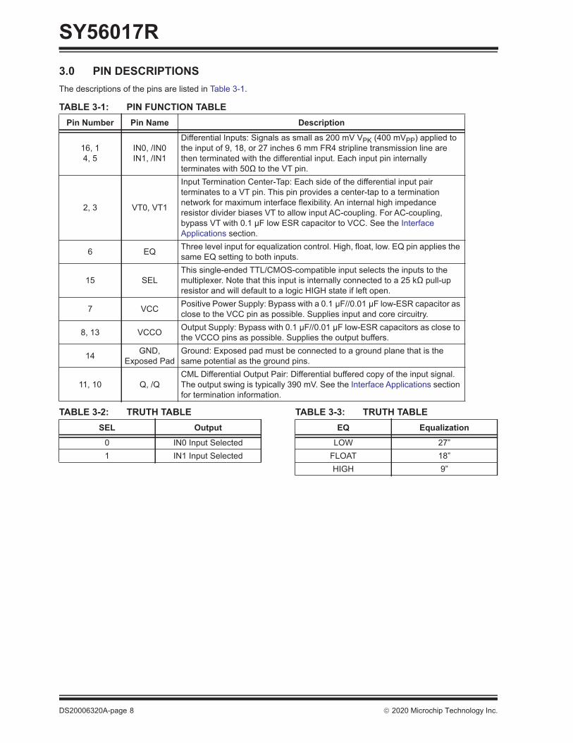
3.0 PIN DESCRIPTIONSThe descriptions of the pins are listed in Table 3-1.
TABLE 3-1: PIN FUNCTION TABLE Pin Number Pin Name Description
16, 14, 5
IN0, /IN0IN1, /IN1
Differential Inputs: Signals as small as 200 mV VPK (400 mVPP) applied to the input of 9, 18, or 27 inches 6 mm FR4 stripline transmission line are then terminated with the differential input. Each input pin internally terminates with 50Ω to the VT pin.
2, 3 VT0, VT1
Input Termination Center-Tap: Each side of the differential input pair terminates to a VT pin. This pin provides a center-tap to a termination network for maximum interface flexibility. An internal high impedance resistor divider biases VT to allow input AC-coupling. For AC-coupling, bypass VT with 0.1 μF low ESR capacitor to VCC. See the Interface Applications section.
6 EQ Three level input for equalization control. High, float, low. EQ pin applies the same EQ setting to both inputs.
15 SELThis single-ended TTL/CMOS-compatible input selects the inputs to the multiplexer. Note that this input is internally connected to a 25 kΩ pull-up resistor and will default to a logic HIGH state if left open.
7 VCC Positive Power Supply: Bypass with a 0.1 μF//0.01 μF low-ESR capacitor as close to the VCC pin as possible. Supplies input and core circuitry.
8, 13 VCCO Output Supply: Bypass with 0.1 μF//0.01 μF low-ESR capacitors as close to the VCCO pins as possible. Supplies the output buffers.
14 GND,Exposed Pad
Ground: Exposed pad must be connected to a ground plane that is the same potential as the ground pins.
11, 10 Q, /QCML Differential Output Pair: Differential buffered copy of the input signal. The output swing is typically 390 mV. See the Interface Applications section for termination information.
TABLE 3-2: TRUTH TABLESEL Output
0 IN0 Input Selected1 IN1 Input Selected
TABLE 3-3: TRUTH TABLEEQ Equalization
LOW 27”FLOAT 18”HIGH 9”

2020 Microchip Technology Inc. DS20006320A-page 9
SY56017RTiming Diagrams
FIGURE 3-1: Propagation Delay.
Input and Output Stage
/IN
VCC
IN
VT
GND
GND
FIGURE 3-2: Simplified Differential Input Buffer.
VCCO
/Q
Q
GND
FIGURE 3-3: Simplified CML Output Buffer.
Single-Ended and Differential Swings
VIN,VOUT
400mV (Typ.)
FIGURE 3-4: Single-Ended Swing.
VDIFF_IN,VDIFF_OUT 800mV (Typ.)
FIGURE 3-5: Differential Swing.

SY56017R
DS20006320A-page 10 2020 Microchip Technology Inc.
4.0 INTERFACE APPLICATIONSFor Input Interface Applications see Figure 4-1 through Figure 4-5 and for CML Output Termination see Figure 4-6 through Figure 4-9.
4.1 Input Termination1.8V CML driver: Terminate input with VT tied to 1.8V. Don’t terminate 100Ω differentially.2.5V CML driver: Terminate input with either VT tied to 2.5V or 100Ω differentially. The input cannot be DC coupled from a 1.2V CML driver.
4.2 CML Output Termination with VCCO 1.2V
For VCCO of 1.2V, Figure 4-6, terminate the output with 50Ω to 1.2V, not 100Ω differentially across the outputs. If AC-coupling is used, Figure 4-9, terminate into 50Ω to 1.2V before the coupling capacitor and then connect to a high value resistor to a reference voltage. Any unused output pair needs to be terminated, do not leave floating.
4.3 CML Output Termination with VCCO 1.8V
For VCCO of 1.8V or 2.5V, Figure 4-6 and Figure 4-7, terminate with either 50Ω to 1.8V or 2.5V or 100Ω differentially across the outputs. AC- or DC-coupling is fine.
Input Interface Applications
CMLIN
/IN
SY56017R
VCC (2.5V)
GND
VTNC
FIGURE 4-1: CML Interface (DC-Coupled, 2.5V, 100Ω Differential).
CMLIN
/IN
SY56017R
VCC (1.8V, 2.5V)
GND
VT
VCC (1.8V, 2.5V)
FIGURE 4-2: CML Interface (DC-Coupled, 1.8V, 2.5V, 50Ω to VCC).
0.1μF
VCC
CMLIN
/IN
SY56017R
VCC(1.8V,2.5V,3.3V)
GND
VT
FIGURE 4-3: CML Interface (AC-Coupled).
LVPECLIN
/IN
SY56017R
VCC (3.3V, 2.5V)
RPRP
For 3.3V, RP For 2.5V, RP
GND
GND VT0.1μF
VCC
FIGURE 4-4: LVPECL Interface (AC-Coupled).

0.1μF
VCC
LVDSIN
/IN
SY56017R
VCC
GND
VT
2020 Microchip Technology Inc. DS20006320A-page 11
SY56017R
FIGURE 4-5: LVDS Interface (AC-Coupled).
CML Output Termination
50Ω50Ω
VCCO (1.2V, 1.8V, 2.5V)
GND
50Ω
IN
/IN
Z0= 50Ω
Z0= 50Ω 50Ω
VCCO(1.2V, 1.8V, 2.5V)
Q
/Q
FIGURE 4-6: 1.2V, 1.8V, or 2.5V CML DC-Coupled Termination.
VCCO (1.8V,2.5V)
FIGURE 4-7: 1.8V or 2.5V CML DC-Coupled Termination.
50Ω50Ω
GND
50Ω
IN
/IN
Z0= 50Ω
Z0= 50Ω 50ΩVBIAS
Q
/Q
VCCO (1.8V,2.5V)
FIGURE 4-8: CML AC-Coupled Termination VCCO 1.8V or 2.5V Only.
FIGURE 4-9: CML AC-Coupled Termination VCCO 1.2V Only.

SY56017R
DS20006320A-page 12 2020 Microchip Technology Inc.
5.0 PACKAGING INFORMATION
5.1 Package Marking Information
XXXX
16-Lead QFN*
WNNN
–R017
Example
5971
–
Legend: XX...X Product code or customer-specific information Y Year code (last digit of calendar year) YY Year code (last 2 digits of calendar year) WW Week code (week of January 1 is week ‘01’) NNN Alphanumeric traceability code Pb-free JEDEC® designator for Matte Tin (Sn) * This package is Pb-free. The Pb-free JEDEC designator ( )
can be found on the outer packaging for this package.●, ▲, ▼ Pin one index is identified by a dot, delta up, or delta down (triangle mark).
Note: In the event the full Microchip part number cannot be marked on one line, it will be carried over to the next line, thus limiting the number of available characters for customer-specific information. Package may or may not include the corporate logo.Underbar (_) and/or Overbar (‾) symbol may not be to scale.
3e
3e

2020 Microchip Technology Inc. DS20006320A-page 13
SY56017R16-Lead QFN 3 mm x 3 mm Package Outline and Recommended Land Pattern
Note: For the most current package drawings, please see the Microchip Packaging Specification located at http://www.microchip.com/packaging.

Note: For the most current package drawings, please see the Microchip Packaging Specification located at http://www.microchip.com/packaging.
SY56017R
DS20006320A-page 14 2020 Microchip Technology Inc.

2020 Microchip Technology Inc. DS20006320A-page 15
SY56017RAPPENDIX A: REVISION HISTORY
Revision A (March 2020)• Converted Micrel document SY56017R to Micro-
chip data sheet template DS20006320A.• Minor text changes throughout.

SY56017R
DS20006320A-page 16 2020 Microchip Technology Inc.
NOTES:
2020 Microchip Technology Inc. DS20006320A-page 17
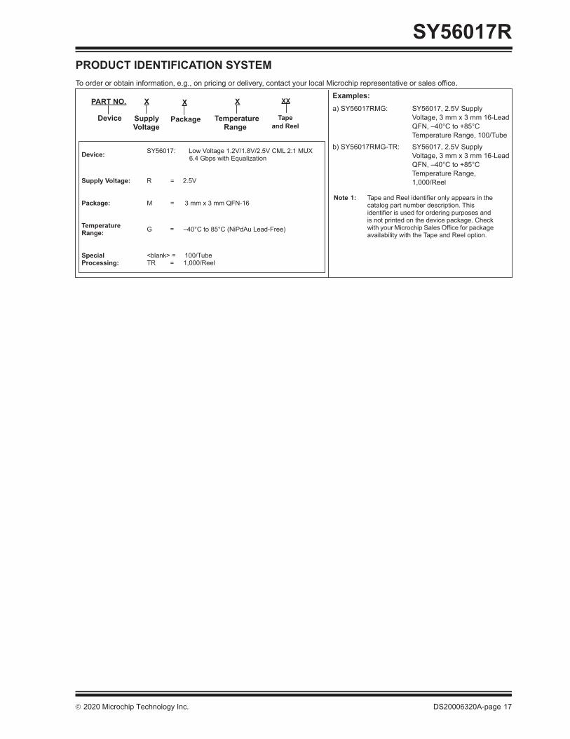
SY56017RPRODUCT IDENTIFICATION SYSTEMTo order or obtain information, e.g., on pricing or delivery, contact your local Microchip representative or sales office.
Examples:a) SY56017RMG: SY56017, 2.5V Supply
Voltage, 3 mm x 3 mm 16-Lead QFN, –40°C to +85°C Temperature Range, 100/Tube
b) SY56017RMG-TR: SY56017, 2.5V Supply Voltage, 3 mm x 3 mm 16-Lead QFN, –40°C to +85°C Temperature Range, 1,000/Reel
PART NO. XX
Package TemperatureRange
Device
Device: SY56017: Low Voltage 1.2V/1.8V/2.5V CML 2:1 MUX 6.4 Gbps with Equalization
Supply Voltage: R = 2.5V
Package: M = 3 mm x 3 mm QFN-16
Temperature Range: G = –40°C to 85°C (NiPdAu Lead-Free)
Special Processing:
<blank> = 100/TubeTR = 1,000/Reel
Note 1: Tape and Reel identifier only appears in the catalog part number description. This identifier is used for ordering purposes and is not printed on the device package. Check with your Microchip Sales Office for package availability with the Tape and Reel option.
X
SupplyVoltage
XX
Tapeand Reel

SY56017R
DS20006320A-page 18 2020 Microchip Technology Inc.
NOTES:
2020 Microchip Technology Inc. DS20006320A-page 19
Information contained in this publication regarding device applications and the like is provided only for your convenience and may be superseded by updates. It is your responsibility to ensure that your application meets with your specifications. MICROCHIP MAKES NO REPRESENTATIONS OR WARRANTIES OF ANY KIND WHETHER EXPRESS OR IMPLIED, WRITTEN OR ORAL, STATUTORY OR OTHERWISE, RELATED TO THE INFORMATION, INCLUDING BUT NOT LIMITED TO ITS CONDITION, QUALITY, PERFORMANCE, MERCHANTABILITY OR FITNESS FOR PURPOSE. Microchip disclaims all liability arising from this information and its use. Use of Microchip devices in life support and/or safety applications is entirely at the buyer’s risk, and the buyer agrees to defend, indemnify and hold harmless Microchip from any and all damages, claims, suits, or expenses resulting from such use. No licenses are conveyed, implicitly or otherwise, under any Microchip intellectual property rights unless otherwise stated.
TrademarksThe Microchip name and logo, the Microchip logo, Adaptec, AnyRate, AVR, AVR logo, AVR Freaks, BesTime, BitCloud, chipKIT, chipKIT logo, CryptoMemory, CryptoRF, dsPIC, FlashFlex, flexPWR, HELDO, IGLOO, JukeBlox, KeeLoq, Kleer, LANCheck, LinkMD, maXStylus, maXTouch, MediaLB, megaAVR, Microsemi, Microsemi logo, MOST, MOST logo, MPLAB, OptoLyzer, PackeTime, PIC, picoPower, PICSTART, PIC32 logo, PolarFire, Prochip Designer, QTouch, SAM-BA, SenGenuity, SpyNIC, SST, SST Logo, SuperFlash, Symmetricom, SyncServer, Tachyon, TempTrackr, TimeSource, tinyAVR, UNI/O, Vectron, and XMEGA are registered trademarks of Microchip Technology Incorporated in the U.S.A. and other countries.
APT, ClockWorks, The Embedded Control Solutions Company, EtherSynch, FlashTec, Hyper Speed Control, HyperLight Load, IntelliMOS, Libero, motorBench, mTouch, Powermite 3, Precision Edge, ProASIC, ProASIC Plus, ProASIC Plus logo, Quiet-Wire, SmartFusion, SyncWorld, Temux, TimeCesium, TimeHub, TimePictra, TimeProvider, Vite, WinPath, and ZL are registered trademarks of Microchip Technology Incorporated in the U.S.A.
Adjacent Key Suppression, AKS, Analog-for-the-Digital Age, Any Capacitor, AnyIn, AnyOut, BlueSky, BodyCom, CodeGuard, CryptoAuthentication, CryptoAutomotive, CryptoCompanion, CryptoController, dsPICDEM, dsPICDEM.net, Dynamic Average Matching, DAM, ECAN, EtherGREEN, In-Circuit Serial Programming, ICSP, INICnet, Inter-Chip Connectivity, JitterBlocker, KleerNet, KleerNet logo, memBrain, Mindi, MiWi, MPASM, MPF, MPLAB Certified logo, MPLIB, MPLINK, MultiTRAK, NetDetach, Omniscient Code Generation, PICDEM, PICDEM.net, PICkit, PICtail, PowerSmart, PureSilicon, QMatrix, REAL ICE, Ripple Blocker, SAM-ICE, Serial Quad I/O, SMART-I.S., SQI, SuperSwitcher, SuperSwitcher II, Total Endurance, TSHARC, USBCheck, VariSense, ViewSpan, WiperLock, Wireless DNA, and ZENA are trademarks of Microchip Technology Incorporated in the U.S.A. and other countries.
SQTP is a service mark of Microchip Technology Incorporated in the U.S.A.The Adaptec logo, Frequency on Demand, Silicon Storage Technology, and Symmcom are registered trademarks of Microchip Technology Inc. in other countries.GestIC is a registered trademark of Microchip Technology Germany II GmbH & Co. KG, a subsidiary of Microchip Technology Inc., in other countries. All other trademarks mentioned herein are property of their respective companies.
© 2020, Microchip Technology Incorporated, All Rights Reserved.
ISBN: 978-1-5224-5816-6
Note the following details of the code protection feature on Microchip devices:• Microchip products meet the specification contained in their particular Microchip Data Sheet.
• Microchip believes that its family of products is one of the most secure families of its kind on the market today, when used in the intended manner and under normal conditions.
• There are dishonest and possibly illegal methods used to breach the code protection feature. All of these methods, to our knowledge, require using the Microchip products in a manner outside the operating specifications contained in Microchip’s Data Sheets. Most likely, the person doing so is engaged in theft of intellectual property.
• Microchip is willing to work with the customer who is concerned about the integrity of their code.
• Neither Microchip nor any other semiconductor manufacturer can guarantee the security of their code. Code protection does not mean that we are guaranteeing the product as “unbreakable.”
Code protection is constantly evolving. We at Microchip are committed to continuously improving the code protection features of our products. Attempts to break Microchip’s code protection feature may be a violation of the Digital Millennium Copyright Act. If such acts allow unauthorized access to your software or other copyrighted work, you may have a right to sue for relief under that Act.
For information regarding Microchip’s Quality Management Systems, please visit www.microchip.com/quality.

DS20006320A-page 20 2020 Microchip Technology Inc.
AMERICASCorporate Office2355 West Chandler Blvd.Chandler, AZ 85224-6199Tel: 480-792-7200 Fax: 480-792-7277Technical Support: http://www.microchip.com/supportWeb Address: www.microchip.comAtlantaDuluth, GA Tel: 678-957-9614 Fax: 678-957-1455Austin, TXTel: 512-257-3370 BostonWestborough, MA Tel: 774-760-0087 Fax: 774-760-0088ChicagoItasca, IL Tel: 630-285-0071 Fax: 630-285-0075DallasAddison, TX Tel: 972-818-7423 Fax: 972-818-2924DetroitNovi, MI Tel: 248-848-4000Houston, TX Tel: 281-894-5983IndianapolisNoblesville, IN Tel: 317-773-8323Fax: 317-773-5453Tel: 317-536-2380Los AngelesMission Viejo, CA Tel: 949-462-9523Fax: 949-462-9608Tel: 951-273-7800 Raleigh, NC Tel: 919-844-7510New York, NY Tel: 631-435-6000San Jose, CA Tel: 408-735-9110Tel: 408-436-4270Canada - TorontoTel: 905-695-1980 Fax: 905-695-2078
ASIA/PACIFICAustralia - SydneyTel: 61-2-9868-6733China - BeijingTel: 86-10-8569-7000 China - ChengduTel: 86-28-8665-5511China - ChongqingTel: 86-23-8980-9588China - DongguanTel: 86-769-8702-9880 China - GuangzhouTel: 86-20-8755-8029 China - HangzhouTel: 86-571-8792-8115 China - Hong Kong SARTel: 852-2943-5100 China - NanjingTel: 86-25-8473-2460China - QingdaoTel: 86-532-8502-7355China - ShanghaiTel: 86-21-3326-8000 China - ShenyangTel: 86-24-2334-2829China - ShenzhenTel: 86-755-8864-2200 China - SuzhouTel: 86-186-6233-1526 China - WuhanTel: 86-27-5980-5300China - XianTel: 86-29-8833-7252China - XiamenTel: 86-592-2388138 China - ZhuhaiTel: 86-756-3210040
ASIA/PACIFICIndia - BangaloreTel: 91-80-3090-4444 India - New DelhiTel: 91-11-4160-8631India - PuneTel: 91-20-4121-0141Japan - OsakaTel: 81-6-6152-7160 Japan - TokyoTel: 81-3-6880- 3770 Korea - DaeguTel: 82-53-744-4301Korea - SeoulTel: 82-2-554-7200Malaysia - Kuala LumpurTel: 60-3-7651-7906Malaysia - PenangTel: 60-4-227-8870Philippines - ManilaTel: 63-2-634-9065SingaporeTel: 65-6334-8870Taiwan - Hsin ChuTel: 886-3-577-8366Taiwan - KaohsiungTel: 886-7-213-7830Taiwan - TaipeiTel: 886-2-2508-8600 Thailand - BangkokTel: 66-2-694-1351Vietnam - Ho Chi MinhTel: 84-28-5448-2100
EUROPEAustria - WelsTel: 43-7242-2244-39Fax: 43-7242-2244-393Denmark - CopenhagenTel: 45-4485-5910 Fax: 45-4485-2829Finland - EspooTel: 358-9-4520-820France - ParisTel: 33-1-69-53-63-20 Fax: 33-1-69-30-90-79 Germany - GarchingTel: 49-8931-9700Germany - HaanTel: 49-2129-3766400Germany - HeilbronnTel: 49-7131-72400Germany - KarlsruheTel: 49-721-625370Germany - MunichTel: 49-89-627-144-0 Fax: 49-89-627-144-44Germany - RosenheimTel: 49-8031-354-560Israel - Ra’anana Tel: 972-9-744-7705Italy - Milan Tel: 39-0331-742611 Fax: 39-0331-466781Italy - PadovaTel: 39-049-7625286 Netherlands - DrunenTel: 31-416-690399 Fax: 31-416-690340Norway - TrondheimTel: 47-7288-4388Poland - WarsawTel: 48-22-3325737 Romania - BucharestTel: 40-21-407-87-50Spain - MadridTel: 34-91-708-08-90Fax: 34-91-708-08-91Sweden - GothenbergTel: 46-31-704-60-40Sweden - StockholmTel: 46-8-5090-4654UK - WokinghamTel: 44-118-921-5800Fax: 44-118-921-5820
Worldwide Sales and Service
02/28/20