Embed Size (px)
Citation preview
LTC2936
12936fa
For more information www.linear.com/LTC2936
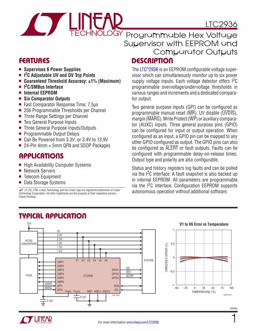
Typical applicaTion
DescripTion
Programmable Hex Voltage Supervisor with EEPROM and
Comparator Outputs
The LTC®2936 is an EEPROM configurable voltage super-visor which can simultaneously monitor up to six power supply voltage inputs. Each voltage detector offers I2C programmable overvoltage/undervoltage thresholds in various ranges and increments and a dedicated compara-tor output.
Two general purpose inputs (GPI) can be configured as programmable manual reset (MR), UV disable (UVDIS), margin (MARG), Write Protect (WP) or auxiliary compara-tor (AUXC) inputs. Three general purpose pins (GPIO) can be configured for input or output operation. When configured as an input, a GPIO pin can be mapped to any other GPIO configured as output. The GPIO pins can also be configured as ALERT or fault outputs. Faults can be configured with programmable delay-on-release times. Output type and polarity are also configurable.
Status and history registers log faults and can be polled via the I2C interface. A fault snapshot is also backed up in internal EEPROM. All parameters are programmable via the I2C interface. Configuration EEPROM supports autonomous operation without additional software.
FeaTures
applicaTions
n Supervises 6 Power Supplies n I2C Adjustable UV and OV Trip Points n Guaranteed Threshold Accuracy: ±1% (Maximum) n I2C/SMBus Interface n Internal EEPROM n Six Comparator Outputs n Fast Comparator Response Time: 7.5µs n 256 Programmable Thresholds per Channel n Three Range Settings per Channel n Two General Purpose Inputs n Three General Purpose Inputs/Outputs n Programmable Output Delays n Can Be Powered from 3.3V, or 3.4V to 13.9V n 24-Pin 4mm × 5mm QFN and SSOP Packages
n High Availability Computer Systems n Network Servers n Telecom Equipment n Data Storage Systems
V1 to V6 Error vs Temperature
LTC2936
CMP1CMP2CMP3CMP4CMP5CMP6GPI1GPI2
5V3.3V2.5V1.8V1.5V1.2V
GPIO1GPIO2GPIO3
SDASCL
V1
ASEL0ASEL1VDD33VPWR GND
V2 V3 V4 V5 V6
FPGA
SYSTEM
DC/DCCONVERTERS
12V
OVRSTALERT
0.1µF0.1µF
2936 TA01a
UVDISMARG
TEMPERATURE (°C)–50
THRE
SHOL
D ER
ROR
(%)
1
0.5
0
–0.5
–125–25 75
2936 TA01b
1000 50
L, LT, LTC, LTM, Linear Technology and the Linear logo are registered trademarks of Linear Technology Corporation. All other trademarks are the property of their respective owners. Patent Pending.
LTC2936
22936fa
For more information www.linear.com/LTC2936
absoluTe MaxiMuM raTingsSupply Voltages
VPWR.......................................................–0.3V to 14V VDD33 .................................................... –0.3V to 3.6V
Digital Input/Output Voltages SDA, SCL, GPI1, GPI2 .............................. –0.3V to 6V GPIO1-GPIO3, CMP1-CMP6 ....................–0.3V to 14V ASEL0, ASEL1 ..................................... –0.3V to VDD33
Analog Voltages V1-V6 ....................................................... –0.3V to 6V
(Notes 1, 2)
1
2
3
4
5
6
7
8
9
10
11
12
TOP VIEW
GN PACKAGE24-LEAD PLASTIC SSOP
24
23
22
21
20
19
18
17
16
15
14
13
V3
V2
V1
VPWR
VDD33
GND
GPIO3
ASEL0
ASEL1
CMP4
CMP3
CMP2
V4
V5
V6
GPI1
GPI2
SCL
SDA
GPIO1
GPIO2
CMP5
CMP6
CMP1
TJMAX = 125°C, θJA = 88°C/W, θJCtop = 30°C/W
8 9
TOP VIEW
25
UFD PACKAGE24-LEAD (4mm × 5mm) PLASTIC QFN
10 11 12
24 23 22 21 20
6
5
4
3
2
1V1
VPWR
VDD33
GND
GPIO3
ASEL0
ASEL1
GPI1
GPI2
SCL
SDA
GPIO1
GPIO2
CMP5V2 V3 V4 V5 V6
CMP4
CMP3
CMP2
CMP1
CMP6
7
14
15
16
17
18
19
13
TJMAX = 125°C, θJA = 43°C/W, θJCbottom = 3.4°C/W
EXPOSED PAD (PIN 25) IS GND PCB CONNECTION IS OPTIONAL
pin conFiguraTion
orDer inForMaTionLEAD FREE FINISH TAPE AND REEL PART MARKING* PACKAGE DESCRIPTION TEMPERATURE RANGE
LTC2936CGN#PBF LTC2936CGN#TRPBF LTC2936GN 24-Lead Plastic SSOP 0°C to 70°C
LTC2936IGN#PBF LTC2936IGN#TRPBF LTC2936GN 24-Lead Plastic SSOP –40°C to 85°C
LTC2936CUFD#PBF LTC2936CUFD#TRPBF 2936 24-Lead (4mm × 5mm) Plastic QFN 0°C to 70°C
LTC2936IUFD#PBF LTC2936IUFD#TRPBF 2936 24-Lead (4mm × 5mm) Plastic QFN –40°C to 85°C
Consult LTC Marketing for parts specified with wider operating temperature ranges. *The temperature grade is identified by a label on the shipping container.For more information on lead free part marking, go to: http://www.linear.com/leadfree/ For more information on tape and reel specifications, go to: http://www.linear.com/tapeandreel/
Operating Temperature Range LTC2936C ................................................ 0°C to 70°C LTC2936I .............................................–40°C to 85°C
Storage Temperature Range ................ –65°C to 150°C*Maximum Junction Temperature ........................ 125°C*Lead Temperature Range (Soldering, 10 sec)
SSOP Package .................................................. 300°C
* See Applications Information section for detailed EEPROM derating information for junction temperatures in excess of 85°C.
http://www.linear.com/product/LTC2936#orderinfo
LTC2936
32936fa
For more information www.linear.com/LTC2936
elecTrical characTerisTics The l denotes the specifications which apply over the full operating temperature range, otherwise specifications are at TA = 25°C and VPWR = 12V (Note 2).
SYMBOL PARAMETER CONDITIONS MIN TYP MAX UNITSPower Supply CharacteristicsVPWR VPWR Supply Voltage Range l 3.4 13.9 V
VDD33 VDD33 Regulator Output Voltage IVDD33 = –1mA l 3.23 3.3 3.37 V
IDD VDD33 Regulator Current Limit VDD33 = 0V l –10 mA
VDDEXT VDD33 Supply Voltage Range VDD33 = VPWR l 3.13 3.3 3.47 V
IPWR VPWR Supply Current Writing to EEPROM
l
l
0.7 1.5
mA mA
IVDDEXT VDDEXT Supply Current Writing to EEPROM
l
l
0.7 1.5
mA mA
Voltage Supervisor CharacteristicsVRANGE Vn Monitoring Range Precision Range
Low Range Medium Range
l
l
l
0.2 0.5 1
1.2 3
5.8
V
VSTEP Vn Threshold Programming Step (LSB) Precision Range Low Range Medium Range
4 10 20
mV
VERR Vn Threshold Accuracy Precision Range, 0.6V < Vn < 1.2V Precision Range, 0.2V < Vn < 0.6V Low Range, 1.5V < Vn < 3V Low Range, 0.5V < Vn < 1.5V Medium Range, 3V < Vn < 5.8V Medium Range, 1V< Vn <3V
l
l
l
l
l
l
±1 ±6 ±1
±15 ±1
±30
% mV
% mV
% mV
RIN Vn Input Impedance Low and Medium Range and High Range l 400 600 kΩ
IIN Vn Input Current Precision Range, 1.2V Input l ±10 nA
tRT Vn Comparator Response Time 2 LSB of Overdrive 20 LSB of Overdrive
l
15 7.5
10
µs µs
Manual Reset CharacteristicstMRI Input Pulse Width Active Low l 5 µs
tMRR Glitch Rejection 1 µs
CMPn Output CharacteristicsVOL Low Output Voltage ISINK = 3mA l 0.4 V
ILEAK Leakage Current VCMP = 13.9V l ±2 µA
IPU Internal Pull-up Current VCMP = 2V l –5 –15 –30 µA
GPIn CharacteristicsVITH Input Threshold Voltage l 0.6 1 1.4 V
ILEAK Leakage Current VGPI = 6V l ±2 µA
IPU Internal Pull-up Current VGPI = 2V l –5 –15 –30 µA
Auxiliary Comparator Characteristics VACIN Input Threshold Voltage l 0.49 0.5 0.51 V
IACIN Input Current Input Voltage = 0.5V l ±10 nA
tACRT Response time 40mV Overdrive 25 µs
GPIOn CharacteristicsVOL Low Output Voltage ISINK = 3mA l 0.4 V
VITH Input Threshold Voltage l 0.6 1 1.4 V
ILEAK Leakage Current VGPIO = 13.9V l ±2 µA
IPU Internal Pull-up Current VGPIO = 2V l –5 –15 –30 µA

LTC2936
42936fa
For more information www.linear.com/LTC2936
elecTrical characTerisTics The l denotes the specifications which apply over the full operating temperature range, otherwise specifications are at TA = 25°C and VPWR = 12V (Note 2).
SYMBOL PARAMETER CONDITIONS MIN TYP MAX UNITStDRO Programmable Output Delay-On-Release
GPIO1_DELAY_ON_RELEASE, GPIO2_DELAY_ON_RELEASE and GPIO3_DELAY_ON_RELEASE
000b 001b 010b 011b 100b 101b 110b 111b
l
l
l
l
l
l
l
l
1
4.5 17.9 35.8
143.3 286.6 1146
0.001 1.6 6.4
25.6 51.2
204.8 409.6 1638
0.050 2.1 8.3
33.3 66.6
266.3 532.6 2130
ms ms ms ms ms ms ms ms
EEPROM CharacteristicsRetention Retention (Notes 5, 6) l 10 Years
Endurance Endurance (Notes 5, 6) l 10,000 Cycles
tEEFS Fault Storage Time (Note 4) Backup Fault Storage Operation 10 ms
tEEPR Programming Time I2C NAK’s During STORE_USER Operation 100 ms
tEERU Restore Time RESTORE_USER Command 1 ms
Digital Inputs SCL, SDAVIH High Level Input Voltage l 2.0 V
VIL Low Level Input Voltage l 0.8 V
VHYST Input Hysteresis (Note 4) 40 mV
ILEAK Input Leakage Current SCL, SDA = GND to 5.5V l –1 1 µA
Digital Output SDAVOL Digital Output Low Voltage ISINK = 3mA l 0.4 V
Digital Inputs ASEL0, ASEL1VIH Input High Threshold Voltage l VDD33 –
0.4V
VIL Input Low Threshold Voltage l 0.4 V
IIH,IL High, Low Input Current ASELn = 0, VDD33 l –20 20 µA
IFLOAT High Z Input Current 0.5V< ASELn < VDD33 – 0.5V l –10 10 µA
Serial Bus Timing Characteristics (Note 3)fSCL Serial Clock Frequency l 10 400 kHz
tLOW Serial Clock Low Period l 1.3 µs
tHIGH Serial Clock High Period l 0.6 µs
tBUF Bus Free Time Between Stop and Start l 1.3 µs
tHD,STA Start Condition Hold Time l 600 ns
tSU,STA Start Condition Setup Time l 600 ns
tSU,STO Stop Condition Setup Time l 600 ns
tHD,DAT Data Hold Time LTC2936 Receiving Data l 0 ns
LTC2936 Transmitting Data l 300 ns
tSU,DAT Data Setup Time l 100 ns
tSP Pulse Width of Spike Suppressed 100 ns
tTIMEOUT_BUS Time Allowed to Complete Any PMBus Command After Which Time SDA Will Be Released and Command Terminated
32 ms

LTC2936
52936fa
For more information www.linear.com/LTC2936
Note 1: Stresses beyond those listed under Absolute Maximum Ratings may cause permanent damage to the device. Exposure to any Absolute Maximum Rating condition for extended periods may affect device reliability and lifetime. The LTC2936 is tested with TA = TCASE.Note 2: All currents into device pins are positive; all currents out of device pins are negative. All voltages are referenced to GND unless otherwise specified.Note 3: Maximum capacitive load, CB, for SCL and SDA is 400pF. Data and clock rise time (tr) and fall time (tf) are: (20 + 0.1 • CB) (ns) < tr < 300ns, and (20 + 0.1 • CB) (ns) < tf < 300ns CB = capacitance of one bus line in pF. SCL and SDA external pull-up voltage, VIO, is 3V < VIO < 5.5V.
Note 4: Guaranteed by design, not directly tested.Note 5: EEPROM endurance and retention are guaranteed by design, characterization and correlation with statistical process controls. The minimum retention specification applies for devices whose EEPROM has been cycled less than the minimum endurance specification.Note 6: EEPROM endurance and retention will be degraded when TJ > 85°C.
elecTrical characTerisTics
TiMing DiagraMs
2936 TD1
CMPn
Vn
GPIOn tDRO
tRTtRT
Vn_THR
Vn Supervisor Timing
I2C Timing
2936 TD2
SDA
SCL
tf tr tf tBUFtLOW tSU:DAT tHD:STA tSP
tf
tHD:DAT tHIGH
tHD:STA tSU:STA tSU:STOS P SSr
LTC2936
62936fa
For more information www.linear.com/LTC2936
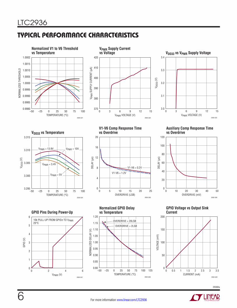
Typical perForMance characTerisTics
V1-V6 Comp Response Time vs Overdrive
GPIO Pins During Power-UpNormalized GPIO Delay vs Temperature
GPIO Voltage vs Output Sink Current
VDD33 vs VPWR Supply Voltage
VDD33 vs TemperatureAuxiliary Comp Response Time vs Overdrive
Normalized V1 to V6 Threshold vs Temperature
VPWR Supply Current vs Voltage
TEMPERATURE (°C)–50
NORM
ALIZ
ED T
HRES
HOLD
1.0002
1.0015
1.0005
0.9995
0.9990
1.0010
1.0000
0.9985
0.998025–25 75
2936 G01
1000 50
OVERDRIVE (mV)0
DELA
Y (µ
s)
120
60
100
80
40
20
0
2936 G06
5010 20 30 40
VPWR VOLTAGE (V)0
V PW
R SU
PPLY
CUR
RENT
(µA)
420
400
390
410
380
37012
2936 G02
153 6 9VPWR VOLTAGE (V)
0
V DD3
3 (V
)
3.4
3.3
3.1
3.2
3.063
2936 G03
15129
OVERDRIVE (LSB)0
DELA
Y (µ
s)
20
8
16
12
4
05 20
2936 G05
2510 15
V1-V6 = 1.2V
V1-V6 = 0.2V
VPWR (V)0
GPIO
(V)
6
5
4
3
2
1
0
2936 G07
62 4
10k PULL-UP FROM GPIOn TO VPWR25°C
TEMPERATURE (°C)–50
NORM
ALIZ
ED D
ELAY
(V)
1.20
1.05
1.15
1.10
1.00
0.95
0.90
0.85
0.80
2936 G08
125–25 0 25 50 75 100
OVERDRIVE = 20LSB
OVERDRIVE = 2LSB
CURRENT (mA)0
VOLT
AGE
(mV)
200
150
100
50
0
2936 G09
3.50.5 1 21.5 2.5 3
TEMPERATURE (°C)–50
V DD3
3 (V
)
3.315
3.310
3.305
3.300
3.295–25 0 75
2936 G04
10025 50
VPWR = 13.9V
VPWR = 3.4V
VPWR = 5V
VPWR = 10V
LTC2936
72936fa
For more information www.linear.com/LTC2936
pin FuncTionsASEL0, ASEL1: I2C Bus Address Select Inputs. Can be connected to ground, VDD33 or can be left unconnected to select 1 out of 9 addresses.
CMP1-CMP6: Comparator Open-Drain Outputs. These pins assert low in response to a user-programmable combina-tion of UV and OV conditions on the associated channels. Each output has a 15µA pull-up to VDD33.
Exposed Pad (QFN Package Only): Ground. The exposed pad may be left open or connected to device ground.
GND: Ground.
GPI1, GPI2: General Purpose Inputs. Configurable as one of five possibilities (no duplication):
• Manual reset (MR) input, active low, 15µA pull-up to VDD33
• UV disable (UVDIS), active low, 15µA pull-up to VDD33. Outputs ignore UV faults.
• Margin (MARG), active low, 15µA pull-up to VDD33. Outputs ignore both UV and OV faults.
• Write Protect (WP), active low, 15µA pull-up to VDD33. I2C write commands are ignored.
• Hi-Z Auxiliary Comparator (AUXC) Input. Program-mable polarity.
GPIO1, GPIO2, GPIO3: General Purpose Input/Output. Each GPIO is configurable as either input, open-drain output, or weak pull-up output. Output polarity is pro-grammable. When configured as outputs, these pins respond to selectable UV conditions, OV conditions, MR, auxiliary comparator output, or other input-configured GPIOn with programmable delay-on-release. These pins can also be configured as ALERT per SMBus standard. When configured as inputs, each pin can be mapped to any other output. These pins have an optional 15µA pull-up to VDD33. Unused GPIO pins should be tied to VDD33 or have their pull-up enabled.
SCL: I2C Serial Clock (400kHz Maximum). Needs external pull-up resistor.
SDA: I2C Serial Data. Needs external pull-up resistor.
V1-V6: Voltage Supervisor Input. Programmable thresh-olds from 0.2V to 1.2V in 4mV increments (precision range), from 0.5V to 3V in 10mV increments (low range) or from 1V to 5.8V in 20mV increments (medium range). See the Applications Information section for information on unused channels.
VDD33: 3.3V Internal Regulator Output. A 100nF capaci-tor to ground is required. The internal regulator can be disabled by connecting VPWR to VDD33 and operating from an external 3.3V supply.
VPWR: Power Supply Input (Internal Regulator Input). Power supply range is 3.4V to 13.9V. Bypass this pin to ground with a 100nF (or greater) capacitor. The internal regulator can be disabled by connecting VPWR to VDD33 and operating from an external 3.3V supply.
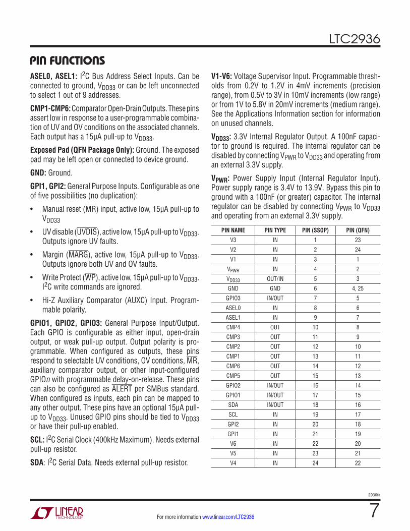
PIN NAME PIN TYPE PIN (SSOP) PIN (QFN)
V3 IN 1 23
V2 IN 2 24
V1 IN 3 1
VPWR IN 4 2
VDD33 OUT/IN 5 3
GND GND 6 4, 25
GPIO3 IN/OUT 7 5
ASEL0 IN 8 6
ASEL1 IN 9 7
CMP4 OUT 10 8
CMP3 OUT 11 9
CMP2 OUT 12 10
CMP1 OUT 13 11
CMP6 OUT 14 12
CMP5 OUT 15 13
GPIO2 IN/OUT 16 14
GPIO1 IN/OUT 17 15
SDA IN/OUT 18 16
SCL IN 19 17
GPI2 IN 20 18
GPI1 IN 21 19
V6 IN 22 20
V5 IN 23 21
V4 IN 24 22
LTC2936
82936fa
For more information www.linear.com/LTC2936
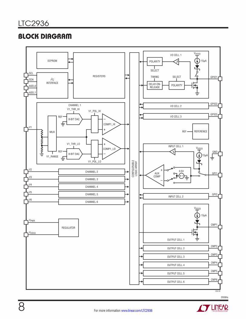
block DiagraM
V1_POL_HI
V1
SCL
COMP1_HI
COMP1_LO
V1_THR_HI
8-BIT DACREF
V1_POL_LO
SDA
ASEL0
ASEL1
I2CINTERFACE
EEPROM
VPWR
V2
CHANNEL 1
V3
V4
V5
V6
VDD33
GND
2936 BD
REGISTERS
GPIO3
VDD33
VDD33
GPIO2
GPIO1
GPI1
15µA
GPI2
I/O CELL 2
INPUT CELL 2
CMP2 OUTPUT CELL 2
OUTPUT CELL 1
I/O CELL 3
I/O CELL 1
DELAY-ON-RELEASE
POLARITY
SELECT
TIMING
POLARITY
SELECT
15µA
INPUT CELL 1
REFERENCEREF
0.5VAUX
COMP
++–
–
V1_THR_LO
8-BIT DACREF
V1_RANGE
MUX
VDD33
CMP1
15µA
CONF
IGUR
ABLE
LOGI
C AR
RAY
CHANNEL 2
CMP3 OUTPUT CELL 3
CMP4 OUTPUT CELL 4
CMP5 OUTPUT CELL 5
CMP6 OUTPUT CELL 6
CHANNEL 3
CHANNEL 4
CHANNEL 5
CHANNEL 6
REGULATOR
+
+
–
–
LTC2936
92936fa
For more information www.linear.com/LTC2936
operaTionThe LTC2936 can perform the following operations:
• Accept I2C bus programming commands.
• Simultaneously monitor up to six inputs with respect to I2C bus programmed fault limits and assert/de-assert the associated CMPn outputs in response to OV and/or UV faults.
• Configure and monitor for OV/UV faults using two independent comparators per channel.
• Configure two general purpose inputs as manual reset (MR), undervoltage disable (UVDIS), margin (MARG), write protect (WP) or auxiliary comparator (AUXC) inputs.
• Configure three general purpose inputs/outputs (GPIOn) to output faults, inputs from GPIn or from other GPIOn.
• Independently select each general purpose output polarity and type (open-drain or weak pull-up).
• Independently select each general purpose output response delay-on-release (with respect to the mo-ment its condition is internally cleared).
• Generate interrupt (ALERT) signals in response to any voltage faults, as well as the logic state of the inputs.
• Store register contents to EEPROM.
• Store voltage and timing fault history to EEPROM.
• Restore EEPROM contents into the operating memory, by I2C command and at power-up.
• Report voltage fault status and history.
• Hardware and/or software write-protect the operating memory.
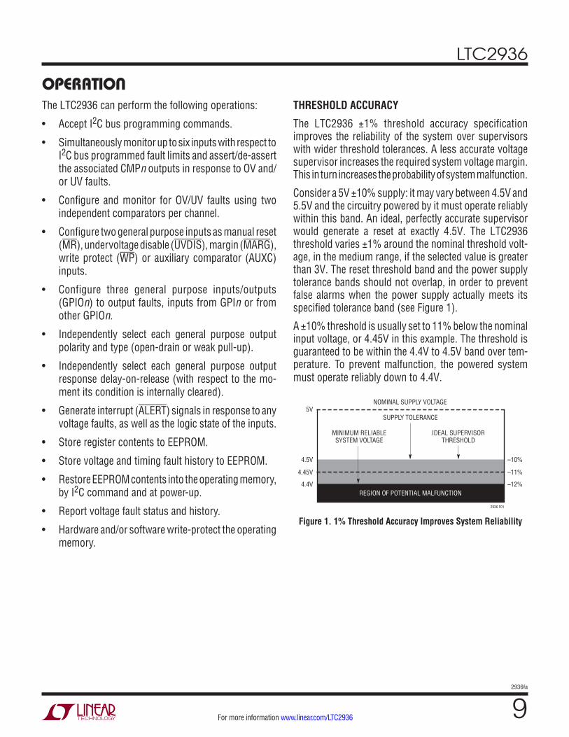
THRESHOLD ACCURACY
The LTC2936 ±1% threshold accuracy specification improves the reliability of the system over supervisors with wider threshold tolerances. A less accurate voltage supervisor increases the required system voltage margin. This in turn increases the probability of system malfunction.
Consider a 5V ±10% supply: it may vary between 4.5V and 5.5V and the circuitry powered by it must operate reliably within this band. An ideal, perfectly accurate supervisor would generate a reset at exactly 4.5V. The LTC2936 threshold varies ±1% around the nominal threshold volt-age, in the medium range, if the selected value is greater than 3V. The reset threshold band and the power supply tolerance bands should not overlap, in order to prevent false alarms when the power supply actually meets its specified tolerance band (see Figure 1).
A ±10% threshold is usually set to 11% below the nominal input voltage, or 4.45V in this example. The threshold is guaranteed to be within the 4.4V to 4.5V band over tem-perature. To prevent malfunction, the powered system must operate reliably down to 4.4V.
Figure 1. 1% Threshold Accuracy Improves System Reliability
NOMINAL SUPPLY VOLTAGE
SUPPLY TOLERANCE
MINIMUM RELIABLESYSTEM VOLTAGE
2936 F01
5V
4.5V
4.4V
4.45V
–10%
–12%
–11%
REGION OF POTENTIAL MALFUNCTION
IDEAL SUPERVISORTHRESHOLD

LTC2936
102936fa
For more information www.linear.com/LTC2936
operaTionI2C Serial Digital Interface
The LTC2936 communicates with a host (master) using the I2C serial bus interface. The Timing Diagram shows the timing relationship of the signals on the bus. The two bus lines, SDA and SCL, must be high when the bus is not in use. External pull-up resistors or current sources are required on these lines.
The LTC2936 is a transmit/receive slave only device. The master device must initiate data transfer on the bus by
generating SCL to allow the transfer. In the event of an OV/UV fault, the LTC2936 can be configured to assert the ALERT output low in order to notify the host.
Slave Address
The LTC2936 can respond to one of 9 addresses. By con-necting the address ASEL0 and ASEL1 inputs to VDD33, GND, or by floating them, the slave address is determined as shown in the following table. The LTC2936 always responds to the special addresses.
LTC2936 Address Look-Up Table
ASEL0 0 Hi-Z 1 0 Hi-Z 1 0 Hi-Z 1
ASEL1 0 0 0 Hi-Z Hi-Z Hi-Z 1 1 1
7-Bit Address 0x50 0x51 0x52 0x53 0x54 0x55 0x58 0x59 0x5A
8-Bit Address 0xA0 0xA2 0xA4 0xA6 0xA8 0xAA 0xB0 0xB2 0xB4
LTC2936 Special Slave Addresses
7-BIT ADDRESS 8-BIT ADDRESS DESCRIPTION
0x0C 0x19 Alert Response Address, Independent of the ASEL pin.
0x73 0xE6 Global address to which all LTC2936's will respond. Independent of the ASEL pin.
SLAVE ADDRESS Wr A A PS
7 81 1 1 11
COMMAND CODE
SLAVE ADDRESS COMMAND CODE DATA BYTE LOWWr A A A PS
7 8 8 1
DATA BYTE HIGH
81 1 1 1 11
A
SLAVE ADDRESS COMMAND CODE SLAVE ADDRESSWr A A A P2936 F00
S
7 8 7 1
DATA BYTE LOW
8
DATA BYTE HIGH
811 1 1
Sr
1 1 11
A
1
Rd A
Communication Protocols
Send Byte Format
Write Word Format
Read Word Format
SSrRdWrAAP
START CONDITIONREPEATED START CONDITIONREAD (BIT VALUE OF 1)WRITE (BIT VALUE OF 0)ACKNOWLEDGE NOT ACKNOWLEDGESTOP CONDITIONMASTER TO SLAVESLAVE TO MASTER
LTC2936
112936fa
For more information www.linear.com/LTC2936
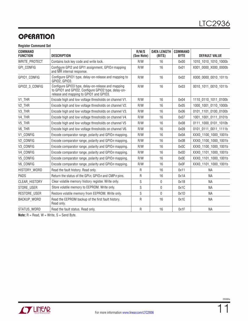
operaTionRegister Command Set
COMMAND FUNCTION DESCRIPTION
R/W/S (See Note)
DATA LENGTH (BITS)
COMMAND BYTE DEFAULT VALUE
WRITE_PROTECT Contains lock key code and write lock. R/W 16 0x00 1010_1010_1010_1000b
GPI_CONFIG Configure GPI2 and GPI1 assignment, GPIOn mapping and MR internal response.
R/W 16 0x01 X001_0000_X000_0000b
GPIO1_CONFIG Configure GPIO1 type, delay-on-release and mapping to GPIO2, GPIO3.
R/W 16 0x02 X000_0000_0010_1011b
GPIO2_3_CONFIG Configure GPIO3 type, delay-on-release and mapping to GPIO1 and GPIO2. Configure GPIO2 type, delay-on-release and mapping to GPIO1 and GPIO3.
R/W 16 0x03 0010_1011_0010_1011b
V1_THR Encode high and low voltage thresholds on channel V1. R/W 16 0x04 1110_0110_1011_0100b
V2_THR Encode high and low voltage thresholds on channel V2. R/W 16 0x05 1000_1001_0110_1000b
V3_THR Encode high and low voltage thresholds on channel V3. R/W 16 0x06 0101_1101_0100_0100b
V4_THR Encode high and low voltage thresholds on channel V4. R/W 16 0x07 1001_1001_0111_0101b
V5_THR Encode high and low voltage thresholds on channel V5 R/W 16 0x08 0111_1000_0101_1010b
V6_THR Encode high and low voltage thresholds on channel V6. R/W 16 0x09 0101_0111_0011_1111b
V1_CONFIG Encode comparator range, polarity and GPIOn mapping. R/W 16 0x0A XXX0_1100_1000_1001b
V2_CONFIG Encode comparator range, polarity and GPIOn mapping. R/W 16 0x0B XXX0_1100_1000_1001b
V3_CONFIG Encode comparator range, polarity and GPIOn mapping. R/W 16 0x0C XXX0_1100_1000_1001b
V4_CONFIG Encode comparator range, polarity and GPIOn mapping. R/W 16 0x0D XXX0_1101_1000_1001b
V5_CONFIG Encode comparator range, polarity and GPIOn mapping. R/W 16 0x0E XXX0_1101_1000_1001b
V6_CONFIG Encode comparator range, polarity and GPIOn mapping. R/W 16 0x0F XXX0_1101_1000_1001b
HISTORY_WORD Read the fault history. Read only. R 16 0x11 NA
PADS Return the status of the GPIn, GPIOn and CMPn pins. R 16 0x1A NA
CLEAR_HISTORY Clear volatile memory history register. Write only. S 0 0x1B NA
STORE_USER Store volatile memory to EEPROM. Write only. S 0 0x1C NA
RESTORE_USER Restore volatile memory from EEPROM. Write only. S 0 0x1D NA
BACKUP_WORD Read the EEPROM backup of the first fault history. Read only.
R 16 0x1E NA
STATUS_WORD Read the fault status. Read only. R 16 0x1F NA
Note: R = Read, W = Write, S = Send Byte.
LTC2936
122936fa
For more information www.linear.com/LTC2936
operaTionDETAILED COMMAND REGISTER DESCRIPTIONS
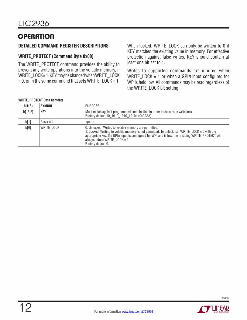
WRITE_PROTECT (Command Byte 0x00)
The WRITE_PROTECT command provides the ability to prevent any write operations into the volatile memory, if WRITE_LOCK = 1. KEY may be changed when WRITE_LOCK = 0, or in the same command that sets WRITE_LOCK = 1.
WRITE_PROTECT Data Contents
BIT(S) SYMBOL PURPOSE
b[15:2] KEY Must match against programmed combination in order to deactivate write lock. Factory default 10_1010_1010_1010b (0x2AAA).
b[1] Reserved Ignore
b[0] WRITE_LOCK 0: Unlocked. Writes to volatile memory are permitted. 1: Locked. Writing to volatile memory is not permitted. To unlock, set WRITE_LOCK = 0 with the appropriate key. If a GPIn input is configured for WP, and is low, then reading WRITE_PROTECT will always return WRITE_LOCK = 1. Factory default 0.
When locked, WRITE_LOCK can only be written to 0 if KEY matches the existing value in memory. For effective protection against false writes, KEY should contain at least one bit set to 1.
Writes to supported commands are ignored when WRITE_LOCK = 1 or when a GPIn input configured for WP is held low. All commands may be read regardless of the WRITE_LOCK bit setting.

LTC2936
132936fa
For more information www.linear.com/LTC2936
operaTionGPI_CONFIG (Command Byte 0x01)
The GPI_CONFIG command configures internal response to a manual reset, sets each GPI function, and option-ally maps GPI pins configured as Manual Reset (MR) or Auxiliary Comparator (AUXC) to one or more GPIO pins.
GPI_CONFIG Data Contents
BIT(S) SYMBOL OPERATIONb[15] Reserved Ignoreb[14] GPI2_MR_RESPONSE Effective only if the input GPI2 is MR configured.
0: Disable CLEAR_HISTORY response. 1: Enable CLEAR_HISTORY response on falling edge of GPI2. Factory default 0.
b[13:11] GPI2_CONFIG 000b: Manual Reset (MR) active low, 15µA pull-up. 001b: Reserved. 010b: Margin (MARG) active low, 15µA pull-up. Overvoltage and undervoltage faults are inhibited. 011b: UV Disable (UVDIS) active low, 15µA pull-up. Undervoltage faults are inhibited. 100b: Write Protect (WP). 101b: Auxiliary Comparator (AUXC) positive input on GPI2. 110b: and 111b: Auxiliary Comparator (AUXC) negative input on GPI2. Factory default 010b.
b[10] MAP_GPI2_TO_GPIO3 0: GPI2 input is not mapped to GPIO3. 1: GPI2 input is mapped to GPIO3 if configured as MR or AUXC. Factory default 0.
b[9] MAP_GPI2_TO_GPIO2 0: GPI2 input is not mapped to GPIO2. 1: GPI2 input is mapped to GPIO2 if configured as MR or AUXC. Factory default 0.
b[8] MAP_GPI2_TO_GPIO1 0: GPI2 input is not mapped to GPIO1. 1: GPI2 input is mapped to GPIO1 if configured as MR or AUXC. Factory default 0.
b[7] Reserved Ignoreb[6] GPI1_MR_RESPONSE Effective only if the input GPI1 is MR configured.
0: Disable CLEAR_HISTORY response. 1: Enable CLEAR_HISTORY response on falling edge of GPI1. Factory default 0.
b[5:3] GPI1_CONFIG 000b: Manual Reset (MR) active low, 15µA pull-up. 001b: Reserved. 010b: Margin (MARG) active low, 15µA pull-up. Overvoltage and undervoltage faults are inhibited. 011b: UV Disable (UVDIS) active low, 15µA pull-up. Undervoltage faults are inhibited. 100b: Write Protect (WP). 101b: Auxiliary Comparator (AUXC) positive input on GPI1. 110b: and 111b: Auxiliary Comparator (AUXC) negative input on GPI1. Factory default 000b.
b[2] MAP_GPI1_TO_GPIO3 0: GPI1 input is not mapped to GPIO3. 1: GPI1 input is mapped to GPIO3 if configured as MR or AUXC. Factory default 0.
b[1] MAP_GPI1_TO_GPIO2 0: GPI1 input is not mapped to GPIO2. 1: GPI1 input is mapped to GPIO2 if configured as MR or AUXC. Factory default 0.
b[0] MAP_GPI1_TO_GPIO1 0: GPI1 input is not mapped to GPIO1. 1: GPI1 input is mapped to GPIO1 if configured as MR or AUXC. Factory default 0.

LTC2936
142936fa
For more information www.linear.com/LTC2936
operaTionGPIO1_CONFIG (Command Byte 0x02)
The GPIO1_CONFIG command configures the GPIO1 mapping, delay-on-release time, output type, and polarity. If GPIO1_TYPE_AND_POLARITY is configured as ALERT (100b or 111b), the output is latched and cleared after the
LTC2936 acknowledges the alert response address (see SMBus protocol), HISTORY_WORD is read, or a CLEAR_HISTORY command is received. Only one GPIOn pin should be configured as ALERT. GPIOn_DELAY_ON_RELEASE does not apply to a GPIOn pin configured as ALERT.
WD_GPIO1_CONFIG Data Contents
BIT(S) SYMBOL OPERATION
b[15:8] Reserved Ignore
b[7] MAP_GPIO1_TO_GPIO3 0: GPIO1 input is not mapped to GPIO3. 1: GPIO1 input is mapped to GPIO3. Factory default 0.
b[6] MAP_GPIO1_TO_GPIO2 0: GPIO1 input is not mapped to GPIO2. 1: GPIO1 input is mapped to GPIO2. Factory default 0.
b[5:3] GPIO1_DELAY_ON_RELEASE 000b: Delay selected is 0. 001b: Delay selected is 1.6ms. 010b: Delay selected is 6.4ms. 011b: Delay selected is 26ms. 100b: Delay selected is 51ms. 101b: Delay selected is 205ms. 110b: Delay selected is 410ms. 111b: Delay selected is 1.64s. Factory default 101b (205ms).
b[2:0] GPIO1_TYPE_AND_POLARITY 000b: Active H input. 001b: Active L input. 010b: Active H open-drain output. 011b: Active L open-drain output. 100b: Active L open-drain ALERT output. 101b: Active H, weak pull-up output. 110b: Active L, weak pull-up output. 111b: Active L, weak pull-up ALERT output. Factory default 011b (Active L open-drain output).

LTC2936
152936fa
For more information www.linear.com/LTC2936
operaTionGPIO2_3_CONFIG (Command Byte 0x03)
The GPIO2_3_CONFIG command configures GPIO2 and GPIO3 mapping, delay-on-release time, output type, and polarity. If GPIO2_TYPE_AND_POLARITY is configured as ALERT (100b or 111b), or GPIO3_TYPE_AND_POLARITY is configured as ALERT (100b or 111b), the output is latched,
and is cleared after the LTC2936 acknowledges the alert response address (see SMBus protocol), HISTORY_WORD is read, or a CLEAR_HISTORY command is received. Only one GPIOn pin should be configured as ALERT. GPIOn_DELAY_ON_RELEASE does not apply to a GPIOn pin configured as ALERT.
GPIO2_3_CONFIG Data Contents
BIT(S) SYMBOL OPERATIONb[15] MAP_GPIO3_TO_GPIO2 0: GPIO3 is not mapped into GPIO2.
1: GPIO3 is mapped into GPIO2. Factory default 0.
b[14] MAP_GPIO3_TO_GPIO1 0: GPIO3 is not mapped into GPIO1. 1: GPIO3 is mapped into GPIO1. Factory default 0.
b[13:11] GPIO3_DELAY_ON_RELEASE 000b: Delay selected is 0. 001b: Delay selected is 1.6ms. 010b: Delay selected is 6.4ms. 011b: Delay selected is 26ms. 100b: Delay selected is 51ms. 101b: Delay selected is 205ms. 110b: Delay selected is 410ms. 111b: Delay selected is 1.64s. Factory default 101b (205ms).
b[10:8] GPIO3_TYPE_AND_POLARITY 000b: Active H input. 001b: Active L input. 010b: Active H open-drain output. 011b: Active L open-drain output. 100b: Active L open-drain ALERT output. 101b: Active H, weak pull-up output. 110b: Active L, weak pull-up output. 111b: Active L, weak pull-up ALERT output. Factory default 011b (Active L open-drain output).
b[7] MAP_GPIO2_TO_GPIO3 0: GPIO2 is not mapped into GPIO3. 1: GPIO2 is mapped into GPIO3. Factory default 0.
b[6] MAP_GPIO2_TO_GPIO1 0: GPIO2 is not mapped into GPIO1. 1: GPIO2 is mapped into GPIO1. Factory default 0.
b[5:3] GPIO2_DELAY_ON_RELEASE 000b: Delay selected is 0. 001b: Delay selected is 1.6ms. 010b: Delay selected is 6.4ms. 011b: Delay selected is 26ms. 100b: Delay selected is 51ms. 101b: Delay selected is 205ms. 110b: Delay selected is 410ms. 111b: Delay selected is 1.64s. Factory default 101b (205ms).
b[2:0] GPIO2_TYPE_AND_POLARITY 000b: Active H input. 001b: Active L input. 010b: Active H open-drain output. 011b: Active L open-drain output. 100b: Active L open-drain ALERT output. 101b: Active H, weak pull-up output. 110b: Active L, weak pull-up output. 111b: Active L, weak pull-up ALERT output. Factory default 011b (Active L open-drain output).
LTC2936
162936fa
For more information www.linear.com/LTC2936
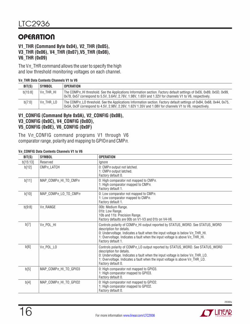
operaTionV1_THR (Command Byte 0x04), V2_THR (0x05), V3_THR (0x06), V4_THR (0x07),V5_THR (0x08), V6_THR (0x09)
The Vn_THR command allows the user to specify the high and low threshold monitoring voltages on each channel.
Vn_THR Data Contents Channels V1 to V6
BIT(S) SYMBOL OPERATION
b[15:8] Vn_THR_HI The COMPn_HI threshold. See the Applications Information section. Factory default settings of 0xE6, 0x89, 0x5D, 0x99, 0x78, 0x57 correspond to 5.5V, 3.64V, 2.76V, 1.98V, 1.65V and 1.32V for channels V1 to V6, respectively.
b[7:0] Vn_THR_LO The COMPn_LO threshold. See the Applications Information section. Factory default settings of 0xB4, 0x68, 0x44, 0x75, 0x5A, 0x3F correspond to 4.5V, 2.98V, 2.26V, 1.62V 1.35V and 1.08V for channels V1 to V6, respectively.
V1_CONFIG (Command Byte 0x0A), V2_CONFIG (0x0B), V3_CONFIG (0x0C), V4_CONFIG (0x0D), V5_CONFIG (0x0E), V6_CONFIG (0x0F)
The Vn_CONFIG command programs V1 through V6 comparator range, polarity and mapping to GPIOn and CMPn.
Vn_CONFIG Data Contents Channels V1 to V6BIT(S) SYMBOL OPERATION
b[15:13] Reserved Ignoreb[12] CMPn_LATCH 0: CMPn output not latched.
1: CMPn output latched. Factory default 0.
b[11] MAP_COMPn_HI_TO_CMPn 0: High comparator not mapped to CMPn. 1: High comparator mapped to CMPn. Factory default 1.
b[10] MAP_COMPn_LO_TO_CMPn 0: Low comparator not mapped to CMPn. 1: Low comparator mapped to CMPn. Factory default 1.
b[9:8] Vn_RANGE 00b: Medium Range. 01b: Low Range. 10b and 11b: Precision Range. Factory defaults are 00b on V1-V3 and 01b on V4-V6.
b[7] Vn_POL_HI Controls polarity of COMPn_HI output reported by STATUS_WORD. See STATUS_WORD description for details. 0: Undervoltage. Indicates a fault when the input voltage is below Vn_THR_HI. 1: Overvoltage. Indicates a fault when the input voltage is above Vn_THR_HI. Factory default 1.
b[6] Vn_POL_LO Controls polarity of COMPn_LO output reported by STATUS_WORD. See STATUS_WORD description for details. 0: Undervoltage. Indicates a fault when the input voltage is below Vn_THR_LO. 1: Overvoltage. Indicates a fault when the input voltage is above Vn_THR_LO. Factory default 0.
b[5] MAP_COMPn_HI_TO_GPIO3 0: High comparator not mapped to GPIO3. 1: High comparator mapped to GPIO3. Factory default 0.
b[4] MAP_COMPn_HI_TO_GPIO2 0: High comparator not mapped to GPIO2. 1: High comparator mapped to GPIO2. Factory default 0.
LTC2936
172936fa
For more information www.linear.com/LTC2936
operaTion
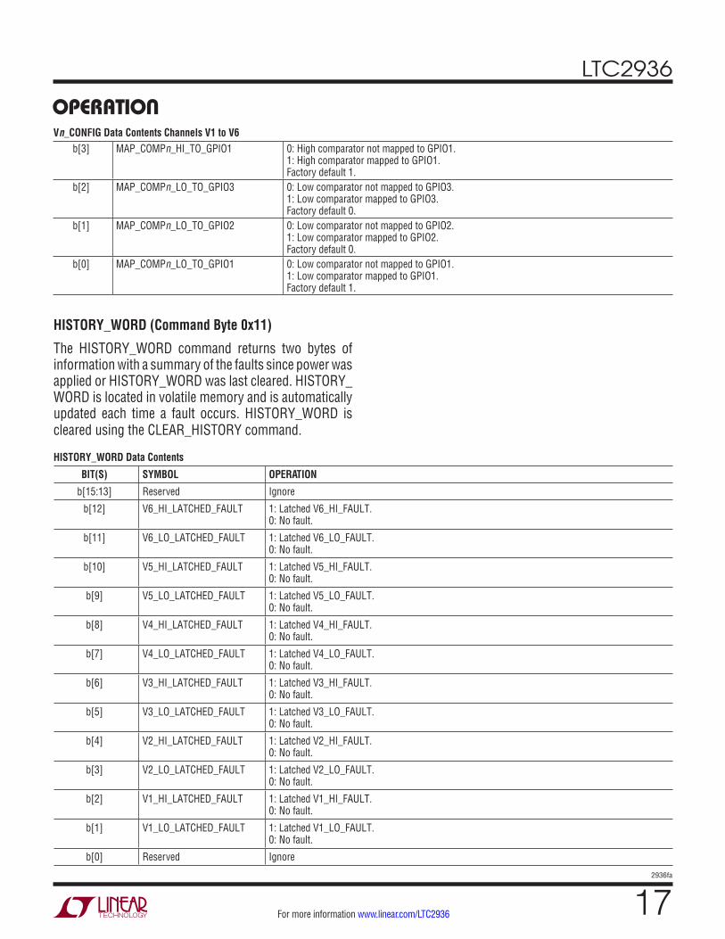
HISTORY_WORD (Command Byte 0x11)
The HISTORY_WORD command returns two bytes of information with a summary of the faults since power was applied or HISTORY_WORD was last cleared. HISTORY_WORD is located in volatile memory and is automatically updated each time a fault occurs. HISTORY_WORD is cleared using the CLEAR_HISTORY command.
HISTORY_WORD Data Contents
BIT(S) SYMBOL OPERATION
b[15:13] Reserved Ignore
b[12] V6_HI_LATCHED_FAULT 1: Latched V6_HI_FAULT. 0: No fault.
b[11] V6_LO_LATCHED_FAULT 1: Latched V6_LO_FAULT. 0: No fault.
b[10] V5_HI_LATCHED_FAULT 1: Latched V5_HI_FAULT. 0: No fault.
b[9] V5_LO_LATCHED_FAULT 1: Latched V5_LO_FAULT. 0: No fault.
b[8] V4_HI_LATCHED_FAULT 1: Latched V4_HI_FAULT. 0: No fault.
b[7] V4_LO_LATCHED_FAULT 1: Latched V4_LO_FAULT. 0: No fault.
b[6] V3_HI_LATCHED_FAULT 1: Latched V3_HI_FAULT. 0: No fault.
b[5] V3_LO_LATCHED_FAULT 1: Latched V3_LO_FAULT. 0: No fault.
b[4] V2_HI_LATCHED_FAULT 1: Latched V2_HI_FAULT. 0: No fault.
b[3] V2_LO_LATCHED_FAULT 1: Latched V2_LO_FAULT. 0: No fault.
b[2] V1_HI_LATCHED_FAULT 1: Latched V1_HI_FAULT. 0: No fault.
b[1] V1_LO_LATCHED_FAULT 1: Latched V1_LO_FAULT. 0: No fault.
b[0] Reserved Ignore
Vn_CONFIG Data Contents Channels V1 to V6b[3] MAP_COMPn_HI_TO_GPIO1 0: High comparator not mapped to GPIO1.
1: High comparator mapped to GPIO1. Factory default 1.
b[2] MAP_COMPn_LO_TO_GPIO3 0: Low comparator not mapped to GPIO3. 1: Low comparator mapped to GPIO3. Factory default 0.
b[1] MAP_COMPn_LO_TO_GPIO2 0: Low comparator not mapped to GPIO2. 1: Low comparator mapped to GPIO2. Factory default 0.
b[0] MAP_COMPn_LO_TO_GPIO1 0: Low comparator not mapped to GPIO1. 1: Low comparator mapped to GPIO1. Factory default 1.

LTC2936
182936fa
For more information www.linear.com/LTC2936
operaTionPADS (Command Byte 0x1A)
The PADS register returns the status of the GPIn, GPIOn and CMPn pads.
PADS Data Contents
BIT(S) SYMBOL OPERATION
b[15:11] Reserved Ignore
b[10] GPI2_STATUS 0: GPI2 pin is logic low. 1: GPI2 pin is logic high.
b[9] GPI1_STATUS 0: GPI1 pin is logic low. 1: GPI1 pin is logic high.
b[8] GPIO3_STATUS 0: GPIO3 pin is logic low. 1: GPIO3 pin is logic high.
b[7] GPIO2_STATUS 0: GPIO2 pin is logic low. 1: GPIO2 pin is logic high.
b[6] GPIO1_STATUS 0: GPIO1 pin is logic low. 1: GPIO1 pin is logic high.
b[5] CMP6_STATUS 0: CMP6 pin is logic low. 1: CMP6 pin is logic high.
b[4] CMP5_STATUS 0: CMP5 pin is logic low. 1: CMP5 pin is logic high.
b[3] CMP4_STATUS 0: CMP4 pin is logic low. 1: CMP4 pin is logic high.
b[2] CMP3_STATUS 0: CMP3 pin is logic low. 1: CMP3 pin is logic high.
b[1] CMP2_STATUS 0: CMP2 pin is logic low. 1: CMP2 pin is logic high.
b[0] CMP1_STATUS 0: CMP1 pin is logic low. 1: CMP1 pin is logic high.
CLEAR_HISTORY (Command Byte 0x1B)
The CLEAR_HISTORY command clears all the faults logged in the volatile HISTORY_WORD register. A manual reset performs the same operation if GPIn_MR_RESPONSE = 1. Clearing HISTORY_WORD does not affect the STATUS_WORD content. Processing of the CLEAR_HISTORY command typically takes less than 10ms, and the part will not acknowledge other I2C operations during that time.
STORE_USER (Command Byte 0x1C) RESTORE_USER (Command Byte 0x1D)
The STORE_USER and RESTORE_USER commands access nonvolatile EEPROM memory. Once a command is
stored in EEPROM using STORE_USER, it will be restored to volatile operating memory with the RESTORE_USER command or when the part powers up.
BACKUP_WORD (Command Byte 0x1E)
After the first fault occurs, HISTORY_WORD is written to EEPROM for backup. Any subsequent BACKUP_WORD write following a fault is inhibited until the CLEAR_HISTORY command is issued. BACKUP_WORD can be retrieved by sending a RESTORE_USER command followed by a BACKUP_WORD read. BACKUP_WORD can be cleared in EEPROM by sending a CLEAR_HISTORY command followed by a STORE_USER command.
LTC2936
192936fa
For more information www.linear.com/LTC2936
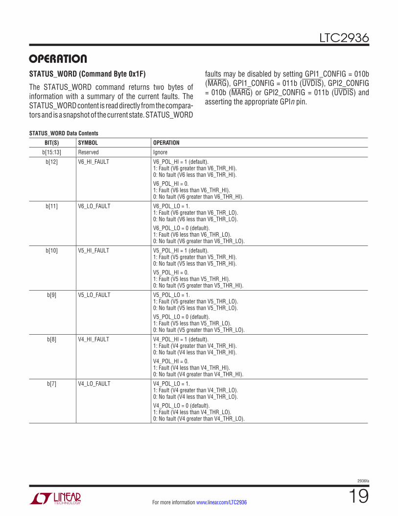
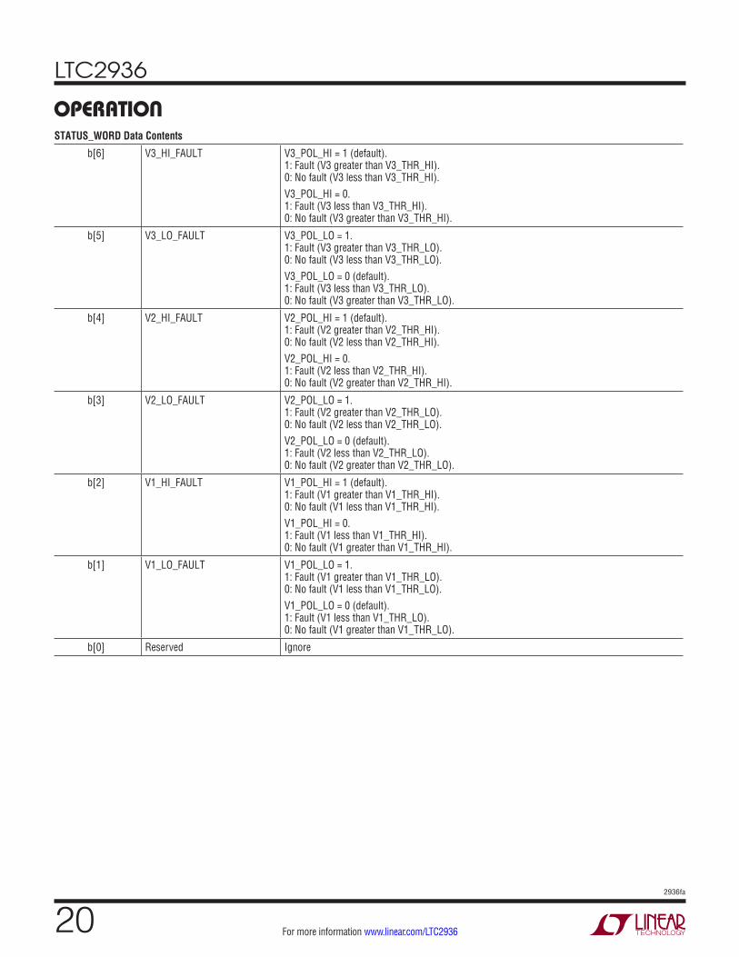
operaTionSTATUS_WORD (Command Byte 0x1F)
The STATUS_WORD command returns two bytes of information with a summary of the current faults. The STATUS_WORD content is read directly from the compara-tors and is a snapshot of the current state. STATUS_WORD
STATUS_WORD Data Contents
BIT(S) SYMBOL OPERATION
b[15:13] Reserved Ignore
b[12] V6_HI_FAULT V6_POL_HI = 1 (default). 1: Fault (V6 greater than V6_THR_HI). 0: No fault (V6 less than V6_THR_HI).V6_POL_HI = 0. 1: Fault (V6 less than V6_THR_HI). 0: No fault (V6 greater than V6_THR_HI).
b[11] V6_LO_FAULT V6_POL_LO = 1. 1: Fault (V6 greater than V6_THR_LO). 0: No fault (V6 less than V6_THR_LO).V6_POL_LO = 0 (default). 1: Fault (V6 less than V6_THR_LO). 0: No fault (V6 greater than V6_THR_LO).
b[10] V5_HI_FAULT V5_POL_HI = 1 (default). 1: Fault (V5 greater than V5_THR_HI). 0: No fault (V5 less than V5_THR_HI).V5_POL_HI = 0. 1: Fault (V5 less than V5_THR_HI). 0: No fault (V5 greater than V5_THR_HI).
b[9] V5_LO_FAULT V5_POL_LO = 1. 1: Fault (V5 greater than V5_THR_LO). 0: No fault (V5 less than V5_THR_LO).V5_POL_LO = 0 (default). 1: Fault (V5 less than V5_THR_LO). 0: No fault (V5 greater than V5_THR_LO).
b[8] V4_HI_FAULT V4_POL_HI = 1 (default). 1: Fault (V4 greater than V4_THR_HI). 0: No fault (V4 less than V4_THR_HI).V4_POL_HI = 0. 1: Fault (V4 less than V4_THR_HI). 0: No fault (V4 greater than V4_THR_HI).
b[7] V4_LO_FAULT V4_POL_LO = 1. 1: Fault (V4 greater than V4_THR_LO). 0: No fault (V4 less than V4_THR_LO).V4_POL_LO = 0 (default). 1: Fault (V4 less than V4_THR_LO). 0: No fault (V4 greater than V4_THR_LO).
faults may be disabled by setting GPI1_CONFIG = 010b (MARG), GPI1_CONFIG = 011b (UVDIS), GPI2_CONFIG = 010b (MARG) or GPI2_CONFIG = 011b (UVDIS) and asserting the appropriate GPIn pin.
LTC2936
202936fa
For more information www.linear.com/LTC2936
operaTionSTATUS_WORD Data Contents
b[6] V3_HI_FAULT V3_POL_HI = 1 (default). 1: Fault (V3 greater than V3_THR_HI). 0: No fault (V3 less than V3_THR_HI).V3_POL_HI = 0. 1: Fault (V3 less than V3_THR_HI). 0: No fault (V3 greater than V3_THR_HI).
b[5] V3_LO_FAULT V3_POL_LO = 1. 1: Fault (V3 greater than V3_THR_LO). 0: No fault (V3 less than V3_THR_LO).V3_POL_LO = 0 (default). 1: Fault (V3 less than V3_THR_LO). 0: No fault (V3 greater than V3_THR_LO).
b[4] V2_HI_FAULT V2_POL_HI = 1 (default). 1: Fault (V2 greater than V2_THR_HI). 0: No fault (V2 less than V2_THR_HI).V2_POL_HI = 0. 1: Fault (V2 less than V2_THR_HI). 0: No fault (V2 greater than V2_THR_HI).
b[3] V2_LO_FAULT V2_POL_LO = 1. 1: Fault (V2 greater than V2_THR_LO). 0: No fault (V2 less than V2_THR_LO).V2_POL_LO = 0 (default). 1: Fault (V2 less than V2_THR_LO). 0: No fault (V2 greater than V2_THR_LO).
b[2] V1_HI_FAULT V1_POL_HI = 1 (default). 1: Fault (V1 greater than V1_THR_HI). 0: No fault (V1 less than V1_THR_HI).V1_POL_HI = 0. 1: Fault (V1 less than V1_THR_HI). 0: No fault (V1 greater than V1_THR_HI).
b[1] V1_LO_FAULT V1_POL_LO = 1. 1: Fault (V1 greater than V1_THR_LO). 0: No fault (V1 less than V1_THR_LO).V1_POL_LO = 0 (default). 1: Fault (V1 less than V1_THR_LO). 0: No fault (V1 greater than V1_THR_LO).
b[0] Reserved Ignore
LTC2936
212936fa
For more information www.linear.com/LTC2936
applicaTions inForMaTionPower Supply
The LTC2936 is powered from the VPWR input and gen-erates a regulated 3.3V supply on the VDD33. A 100nF external capacitor from VPWR to GND is required in order to decouple any supply noise. A 100nF external capacitor from VDD33 to GND is required to properly compensate the internal voltage regulator.
To power the LTC2936 directly from an external 3.3V power supply, connect the VPWR and VDD33 pins together and connect them to the external 3.3V supply. This mode of operation is useful for reducing power dissipation.
Power-Up Condition
When power is applied, the part turns on and the EEPROM contents are loaded into the volatile operating memory. This operation typically takes less than 200µs.
Voltage Threshold Programming
The medium range is based on a full scale of 0.9V to 6V. The 8-bit programming step size is 20mV. On the medium range, threshold accuracy below 1V and above 5.8V is not specified, but the thresholds are reachable.
The command byte for the voltage threshold can be cal-culated for the medium range with the following equation:
Command Byte = ROUND [50 • (VTH – 0.9)]
The low range is based on a full scale of 0.45V to 3V. The 8-bit programming step size is 10mV. On the low range, threshold accuracy below 0.5V is not specified, but the thresholds are reachable.
The command byte for the voltage threshold can be calculated for the low range with the following equation:
Command Byte = ROUND [100 • (VTH – 0.45)]
The precision range is based on a full scale of 0.18V to 1.2V. The 8-bit programming step size is 4mV. On the low range, threshold accuracy below 0.2V is not specified, but the thresholds are reachable.
The command byte for the voltage threshold can be calculated for the V2 to V6 precision range with the fol-lowing equation:
Command Byte = ROUND [250 • (VTH – 0.18)]
Unused Channels
The user must connect all unused channel inputs to ground , program their configuration words (Vn_CONFIG) to 0x01C0, and program their thresholds (Vn_THR) to 0x0000 in order to avoid false faults.
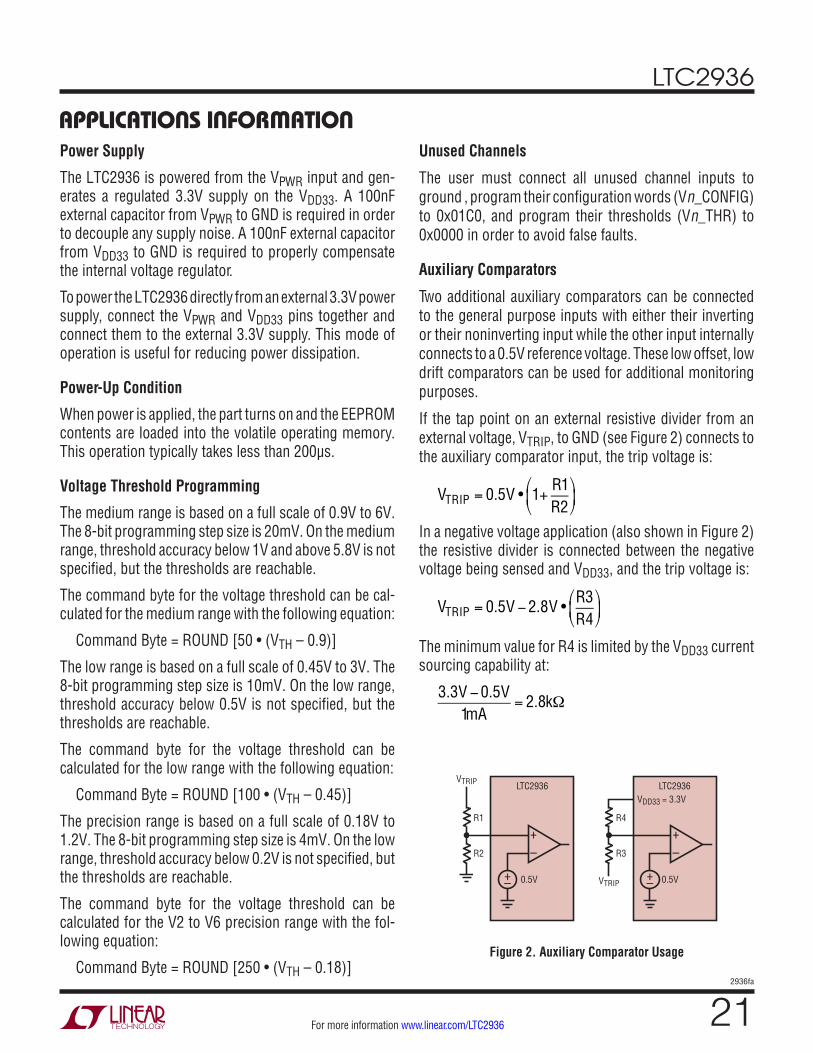
Auxiliary Comparators
Two additional auxiliary comparators can be connected to the general purpose inputs with either their inverting or their noninverting input while the other input internally connects to a 0.5V reference voltage. These low offset, low drift comparators can be used for additional monitoring purposes.
If the tap point on an external resistive divider from an external voltage, VTRIP, to GND (see Figure 2) connects to the auxiliary comparator input, the trip voltage is:
VTRIP = 0.5V • 1+
R1R2
⎛
⎝⎜
⎞
⎠⎟
In a negative voltage application (also shown in Figure 2) the resistive divider is connected between the negative voltage being sensed and VDD33, and the trip voltage is:
VTRIP = 0.5V − 2.8V • R3
R4⎛
⎝⎜
⎞
⎠⎟
The minimum value for R4 is limited by the VDD33 current sourcing capability at:
3.3V − 0.5V1mA
= 2.8kΩ
Figure 2. Auxiliary Comparator Usage
VTRIP
R2
R1
+–
+–
LTC2936VDD33 = 3.3V
R3
0.5V 0.5V
LTC2936
R4
+–
+–VTRIP
LTC2936
222936fa
For more information www.linear.com/LTC2936
applicaTions inForMaTionManual Reset
When a GPIn pin is configured as MR, the in-put is active low. If GPIn_MR_RESPONSE = 1, the HISTORY_WORD register is cleared when MR is pulled low. An internal 15µA current source pulls MR to VDD33. The MR input can also be mapped to a GPIO pin and com-bined with COMPn_HI and COMPn_LO faults to generate a system reset signal.
UV Disable
When a GPIn pin is configured as UVDIS, the input is active low. When UVDIS is grounded, the LTC2936 does not respond to UV type faults. This feature is useful when power cycling the monitored supply. An internal 15µA current source pulls UVDIS to VDD33.
Margin
When a GPIn pin is configured as MARG, the input is active low. When MARG is grounded, the LTC2936 does not respond to any OV or UV faults. This feature is useful when margining the monitored supply. An internal 15µA current source pulls MARG to VDD33.
Outputs
The GPIOn and CMPn outputs are open-drain, with an internal 15µA current source pulling to VDD33 (optional on the GPIOn outputs) and can tolerate a pull-up voltage up to 14V.
All faults, GPIn, or other GPIOn inputs mapped to a GPIOn output are combined with a logical OR function.
The GPIOn pins have programmable delay-on-release timing. The GPIOn pin asserts its active state immediately and de-asserts after the delay-on-release time has elapsed. Any fault causing a GPIOn pin to assert while its delay-on-release timer is active will reset the delay-on-release timer.
When a GPIOn indicates an alert, the alert may be cleared using the standard SMBus Alert Response Address (ARA) protocol. Alerts may also be cleared by reading (or clear-ing) HISTORY_WORD unless the condition causing the alert persists.
The CMPn outputs can be configured as non-latching (default) or latching. Latched CMPn outputs can be reset
by asserting MR low or by issuing a CLEAR_HISTORY command. The CMPn outputs are active low.
Write Protect Features
When the WRITE_LOCK bit is set high, or a GPIn pin configured as WP is pulled low, all I2C write word com-mands are ignored. This feature protects against accidental writing. The lock bit may still be written when the device is write-protected if the provided value for KEY matches the value in memory.
EEPROM
The user may save and restore configuration data to the operating memory registers at any time with STORE_USER and RESTORE_USER commands. Upon power-up, user-stored data is automatically loaded into the operating memory. The part ignores I2C commands while performing EEPROM transactions.
Nondestructive operation above TA = 85°C is possible, but may result in a slight degradation of the retention characteristics. The degradation in EEPROM retention for temperatures exceeding 85°C can be approximated by calculating the acceleration factor:
AF = e
Eak
⎛⎝⎜
⎞⎠⎟•
1TUSE +273
−1
TSTRESS+273
⎛
⎝⎜⎞
⎠⎟⎡
⎣⎢
⎤
⎦⎥
where: AF = acceleration factor Ea = activation energy = 1.5eV k = 8.617 • 10–5 eV/°K TUSE = 85°C maximum specified junction temperature TSTRESS = actual junction temperature °C
Example: calculate effect on retention when operating at a junction temperature of 95°C for 10 hours.
TSTRESS = 95°C, TUSE = 85°C, AF = 3.74
So the overall retention of the EEPROM was degraded by 37.4 hours as a result of operation at a junction tem-perature of 95°C for 10 hours. Note that the effect of this overstress is negligible when compared to the overall EEPROM retention rating of 10 years (87,600 hours) at a temperature of 85°C.

LTC2936
232936fa
For more information www.linear.com/LTC2936
applicaTions inForMaTionNegative Supply Power Monitor
Figure 3 illustrates how to configure the LTC2936 to moni-tor a negative supply rail. Assume the need to monitor the following supply rails: 1.5V, 3.3V, 5V and –5V, within a ±5% system specification.
Channels V1 and V2 are set to medium range, channel V3 is set to low range, channel V4 is set to precision range, and channels V5 and V6 are not used.
Select medium range for V1 and V2 (1V to 6V):
V1_THR_HI = ROUND[50 • (5 • 1.06 – 0.9)] = 220
V1_THR_LO = ROUND[50 • (5 • 0.94 – 0.9)] = 190
V2_THR_HI = ROUND[50 • (3.3 • 1.06 – 0.9)] = 130
V2_THR_LO = ROUND[50 • (3.3 • 0.94 – 0.9)] = 110
Select low range for V3 (0.5V to 3V):
V3_THR_HI = ROUND[100 • (1.5 • 1.06 –0.45)] = 114
V3_THR_LO = ROUND[100 • (1.5 • 0.94 –0.45)] = 96
To monitor –5V, use an external resistive divider connected between VDD33 and the negative rail. The voltage at VDD33 is 3.3V. In order to minimize the error introduced by the leakage current into the V4 input pin, the output of this divider is targeted to lie within the precision voltage range (0.2V to 1.2V). The OV and UV thresholds for the –5V rail are calculated as follows:
V5MIN =3.3 •R1( ) −1.05 • 5 •R2( )
R1+R2> 0.2V
V5MAX =3.3 •R1( ) − 0.95 • 5 •R2( )
R1+R2< 1.2V
Figure 3. Negative Power Supply Monitor
LTC2936
VDD33
GPI1
12V5V3.3V1.5V–5V
5V3.3V1.5V–5V
R1270k
NOTE: INTERNAL GPIO1-3 PULL-UP ENABLED
R2100k
0.1µF
GPIO1GPIO2GPIO3
SDASCL
GPI2
V1
ASEL0 ASEL1
VPWR
GND
V2 V3 V4 V6
SYSTEM
4.7k4.7k
DC/DC
RSTOV
ALERT
MARG
MR
0.1µF
2936 F03
V5

LTC2936
242936fa
For more information www.linear.com/LTC2936
applicaTions inForMaTionR1 = 270k ±0.1% and R2 = 100k ±0.1% satisfy the previous relationships. The programming codes can be calculated as shown in the following equations:
V4MIN =
3.3 • 0.98( ) • 270 • 0.999( ) − 1.05 • 5( ) • 100 •1.001( )
270 • 0.999( ) + 100 •1.001( ) = 0.938V
V4MAX =
3.3 •1.02( ) • 270 •1.001( ) − 0.95 • 5( ) • 100 • 0.999( )
270 •1.001( ) + 100 • 0.999( ) = 1.176V
V4_THR_HI = ROUND[250 • (0.938 • 0.99 – 0.18)] = 187
V4_THR_LO = ROUND[250 • (1.176 • 1.01 – 0.18)] = 252
The normal polarities of the OV and UV comparators need to be swapped, since a drop of the negative supply below its specified absolute value increases V4MAX beyond its encoded threshold. An increase of the negative supply above its specified absolute value decreases V4MIN below its encoded threshold.
The GPIOn outputs are programmed as RST (active low system reset), OV (active low system OV) and ALERT (active low ALERT, see SMBus specification). The UV comparators are mapped to GPIO1 and GPIO3. The OV comparators are mapped to GPIO2 and GPIO3. The GPI1 input is configured as MR (manual reset) and is mapped to GPIO1. The GPI2 input is configured as MARG (margin testing) allowing the system to disable OV and UV faults during margin testing.

LTC2936
252936fa
For more information www.linear.com/LTC2936
applicaTions inForMaTionFive Supply Power-Up Sequencer
Figure 4 illustrates how to use the LTC2936 CMPn outputs to enable DC/DC converters sequentially, at power-up. The system is powered by a 12V source, which is also monitored.
The system starts-up when the pushbutton is pressed and the LTC2950-1 takes the RUN pin of the LTM4600 high. This forces the LTM4600 to generate 5V, which also supplies the other 4 DC/DC converters.
The LTC2936 is configured to monitor 5V on V1, 3.3V on V2, 2.5V on V3, –5V on V4, 1.8V on V5 and 12V on V6. When the programmed threshold is reached on V1, CMP1
pulls high, which enables the 3.3V converter. When the programmed threshold is reached on V2, CMP2 pulls high, which enables the 2.5V converter. When all converters have been enabled and power is good, CMP5 pulls high. GPIO1 is configured to pull high 6.4ms after CMP5.
If the KILL input of the LTC2950-1 is not forced high within 512ms of initial power-up, EN pulls low and the LTM4600 is powered down.
In the event that the external 12V supply drops below its programmed threshold, CMP6 and GPIO2 will pull low after 1.6ms. The LTC2950-1 then receives a logic low on the KILL input, which powers down the LTM4600 and the sequencing circuit.
Figure 4. Five Supply Power-Up Sequencer
2936 F04
LTC2936
CMP1CMP2CMP3CMP4VPWRGPIO1GPIO2GPI1
CMP5CMP6
SDASCL
GPI2
V1
ASEL1 VDD33GND
V2 V3 V4 V5 V6LTM4600
12V
ASEL0
5V
–5V
1.8V
2.5V
3.3V
–5V
1.8V
2.5V
3.3V
5V
10k 10k 10k10k
DONE12V STATUS
LT3704VIN VOUT
RUN/UVLO
LT3028VIN VOUT
SHDN
LT3028VIN VOUT
SHDN
LT3028VIN VOUT
SHDN10k
10k
10k
10k
VIN VOUT
GNDRUN
LTC2950-1VIN EN INT
KILLGNDPB
ON/OFF0.1µF
10k
0.1µF
SYSTEM
270k
0.1µF
100k
1M
100k

LTC2936
262936fa
For more information www.linear.com/LTC2936
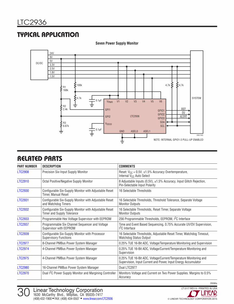
applicaTions inForMaTionSeven Power Supply Monitor
Figure 5 illustrates how to use the LTC2936 auxiliary comparators to expand power supply monitoring to seven channels. The system is powered by a 5V source, which is also monitored. The 9V rail can be monitored, in addition to the six input channels (5V, 3.3V, 2.5V, 1.8V, 1.5V and 24V), using an external resistive divider which feeds the OV and UV tap voltages to the auxiliary comparators on inputs GPI1 and GPI2.
Since the auxiliary comparators’ thresholds are fixed at 0.5V ±10mV, to monitor a 9V ±10% power supply, the following equations apply:
R2+R3R1+R2+R3
=0.51V
0.9 • 9VR3
R1+R2+R3=
0.49V1.1• 9V
For R3 = 8.87k, the equations yield: R2 = 2.4k and R1 = 168k.
The GPI1 comparator monitors the UV limit and is pro-grammed for negative polarity. The GPI2 comparator moni-tors the OV limit and is programmed for positive polarity.
A second resistive divider is used to divide the 24V rail voltage down to 1.08V, in order to use the low leakage, low range of the V6 channel.
Figure 5. Seven Power Supply Monitor
LTC2936
GPI1
GPI2
VDD33
24V9V5V3.3V2.5V1.8V1.5V
100kR1168k
4.7k
0.1µF
GPIO1GPIO2GPIO3
SDASCL
V1
ASEL0 ASEL1
VPWR
GND
V2 V3 V4 V5 V6
SYSTEM
DC/DC
RSTOV
ALERT
0.1µF
R22.4k
R38.87k
2936 F05
4.7k 4.7k
NOTE: INTERNAL GPIO1-3 PULL-UP ENABLED
LTC2936
272936fa
For more information www.linear.com/LTC2936
package DescripTion
GN Package24-Lead Plastic SSOP (Narrow .150 Inch)
(Reference LTC DWG # 05-08-1641)
Please refer to http://www.linear.com/product/LTC2936#packaging for the most recent package drawings.
.337 – .344*(8.560 – 8.738)
GN24 (SSOP) 0204
1 2 3 4 5 6 7 8 9 10 11 12
.229 – .244(5.817 – 6.198)
.150 – .157**(3.810 – 3.988)
161718192021222324 15 1413
.016 – .050(0.406 – 1.270)
.015 ± .004(0.38 ± 0.10)
× 45°
0° – 8° TYP.0075 – .0098(0.19 – 0.25)
.0532 – .0688(1.35 – 1.75)
.008 – .012(0.203 – 0.305)
TYP
.004 – .0098(0.102 – 0.249)
.0250(0.635)
BSC
.033(0.838)
REF
.254 MIN
RECOMMENDED SOLDER PAD LAYOUT
.150 – .165
.0250 BSC.0165 ± .0015
.045 ± .005
* DIMENSION DOES NOT INCLUDE MOLD FLASH. MOLD FLASH SHALL NOT EXCEED 0.006" (0.152mm) PER SIDE** DIMENSION DOES NOT INCLUDE INTERLEAD FLASH. INTERLEAD FLASH SHALL NOT EXCEED 0.010" (0.254mm) PER SIDE
INCHES(MILLIMETERS)
NOTE:1. CONTROLLING DIMENSION: INCHES
2. DIMENSIONS ARE IN
3. DRAWING NOT TO SCALE

LTC2936
282936fa
For more information www.linear.com/LTC2936
package DescripTion
UFD Package24-Lead Plastic QFN (4mm × 5mm)
(Reference LTC DWG # 05-08-1696 Rev A)
Please refer to http://www.linear.com/product/LTC2936#packaging for the most recent package drawings.
4.00 ± 0.10(2 SIDES)
5.00 ± 0.10(2 SIDES)
NOTE:1. DRAWING PROPOSED TO BE MADE A JEDEC PACKAGE OUTLINE MO-220 VARIATION (WXXX-X).2. DRAWING NOT TO SCALE3. ALL DIMENSIONS ARE IN MILLIMETERS4. DIMENSIONS OF EXPOSED PAD ON BOTTOM OF PACKAGE DO NOT INCLUDE MOLD FLASH. MOLD FLASH, IF PRESENT, SHALL NOT EXCEED 0.15mm ON ANY SIDE5. EXPOSED PAD SHALL BE SOLDER PLATED6. SHADED AREA IS ONLY A REFERENCE FOR PIN 1 LOCATION ON THE TOP AND BOTTOM OF PACKAGE
PIN 1TOP MARK(NOTE 6)
0.40 ± 0.10
23 24
1
2
BOTTOM VIEW—EXPOSED PAD
0.75 ± 0.05R = 0.115TYP
R = 0.05 TYP PIN 1 NOTCHR = 0.20 OR C = 0.35
0.25 ± 0.05
0.50 BSC
0.200 REF
0.00 – 0.05
(UFD24) QFN 0506 REV A
RECOMMENDED SOLDER PAD PITCH AND DIMENSIONSAPPLY SOLDER MASK TO AREAS THAT ARE NOT SOLDERED
0.70 ± 0.05
0.25 ± 0.050.50 BSC
2.65 ± 0.052.00 REF
3.00 REF4.10 ± 0.055.50 ± 0.05
3.10 ± 0.05
4.50 ± 0.05
PACKAGE OUTLINE
2.65 ± 0.10
2.00 REF
3.00 REF3.65 ± 0.10
3.65 ± 0.05
LTC2936
292936fa
For more information www.linear.com/LTC2936
Information furnished by Linear Technology Corporation is believed to be accurate and reliable. However, no responsibility is assumed for its use. Linear Technology Corporation makes no representa-tion that the interconnection of its circuits as described herein will not infringe on existing patent rights.
revision hisToryREV DATE DESCRIPTION PAGE NUMBER
A 0117 Added 4.7k pull-ups in Figure 3. 23
LTC2936
302936fa
For more information www.linear.com/LTC2936 LINEAR TECHNOLOGY CORPORATION 2015
LT 0117 REV A • PRINTED IN USALinear Technology Corporation1630 McCarthy Blvd., Milpitas, CA 95035-7417(408) 432-1900 FAX: (408) 434-0507 www.linear.com/LTC2936
relaTeD parTs
Typical applicaTionSeven Power Supply Monitor
PART NUMBER DESCRIPTION COMMENTS
LTC2908 Precision Six-Input Supply Monitor Reset: VCC = 0.5V, ±1.5% Accuracy Overtemperature, Internal VCC Auto Select
LTC2910 Octal Positive/Negative Supply Monitor 8 Adjustable Inputs (0.5V), ±1.5% Accuracy, Input Glitch Rejection, Pin-Selectable Input Polarity
LTC2930 Configurable Six-Supply Monitor with Adjustable Reset Timer, Manual Reset
16 Selectable Thresholds
LTC2931 Configurable Six-Supply Monitor with Adjustable Reset and Watchdog Timers
16 Selectable Thresholds, Threshold Tolerance, Separate Voltage Monitor Outputs
LTC2932 Configurable Six-Supply Monitor with Adjustable Reset Timer and Supply Tolerance
16 Selectable Thresholds, Reset Timer, Separate Voltage Monitor Outputs
LTC2933 Programmable Hex Voltage Supervisor with EEPROM 256 Programmable Thresholds, EEPROM, I2C Interface
LTC2937 Programmable Six Channel Sequencer and Voltage Supervisor with EEPROM
Time and Event Based Sequencing, 0.75% Accurate UV/OV Supervision, I2C Interface
LTC2939 Configurable Six-Supply Monitor with Processor Supervisory Functions
16 Selectable Thresholds, Adjustable Reset Timer, Watchdog Timeout, Watchdog Status Output
LTC2977 8-Channel PMBus Power System Manager 0.25% TUE 16-Bit ADC, Voltage/Temperature Monitoring and Supervision
LTC2974 4-Channel PMBus Power System Manager 0.25% TUE 16-Bit ADC, Voltage/Current/Temperature Monitoring and Supervision
LTC2975 4-Channel PMBus Power System Manager 0.25% TUE 16-Bit ADC, Voltage/Current/Temperature Monitoring and Supervision, Input Current and Power, Input Energy Accumulator
LTC2980 16-Channel PMBus Power System Manager Dual LTC2977
LTC2970 Dual I2C Power Supply Monitor and Margining Controller Monitors Voltage and Current on Two Power Supplies. Margins to 0.5% Accuracy
LTC2936
GPI1
GPI2
VDD33
NOTE: INTERNAL GPIO1-3 PULL-UP ENABLED
24V9V5V3.3V2.5V1.8V1.5V
100kR1168k
4.7k
0.1µF
GPIO1GPIO2GPIO3
SDASCL
V1
ASEL0 ASEL1
VPWR
GND
V2 V3 V4 V5 V6SYSTEM
DC/DC
RSTOV
ALERT
R22.4k
R38.87k
0.1µF
2936 TA02
4.7k 4.7k


