Embed Size (px)
DESCRIPTION
LOW TEMPERATURE PLASMA STUDIES AND APPLICATIONS. Xiaogang Wang Dalian University of Technology. OUTLINE. Relationship with Industry Major Applications Plasma Sources Beams Pulsed Power Technology Atmospheric Pressure Discharge Plasma Etching Dusty Plasma Applications - PowerPoint PPT Presentation
Citation preview

LOW TEMPERATURE PLASMA STUDIES AND APPLICATIONS
Xiaogang Wang Dalian University of Technology

OUTLINERelationship with IndustryMajor Applications Plasma Sources Beams Pulsed Power Technology Atmospheric Pressure Discharge Plasma Etching
Dusty Plasma ApplicationsBiophysical ApplicationsDiscussions
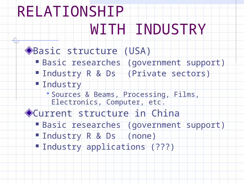
RELATIONSHIP WITH INDUSTRY
Basic structure (USA) Basic researches (government support) Industry R & Ds (Private sectors) Industry
Sources & Beams, Processing, Films, Electronics, Computer, etc.
Current structure in China Basic researches (government support) Industry R & Ds (none) Industry applications (???)

Basic researches (in US)
Pure scientific researches What is going to happen in 20 years?
Such as: computer beyond silicon Basic physical, chemical, biological
processes
“Basic” applied researches New sources, new ways, new materials
Such as: helicon in 90s, sources & beams for “big science” , PSII in 80s, pulsed tech, OAPUGD
Computer codes
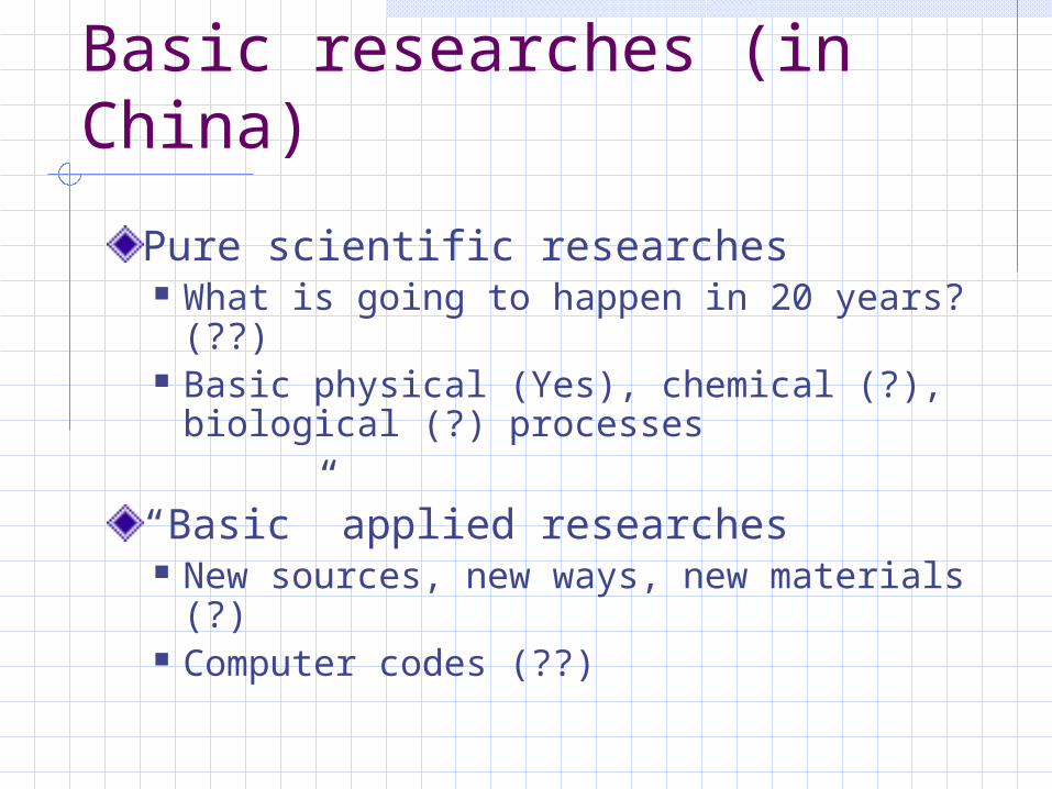
Basic researches (in China)
Pure scientific researches What is going to happen in 20 years? (??) Basic physical (Yes), chemical (?),
biological (?) processes
“Basic” applied researches New sources, new ways, new materials
(?) Computer codes (??)

Industry R & Ds (in US)New sources, new ways, new materials Overlap with basic researches, more
profit-oriented
Computer codes Overlap with basic researches, more
specific
New processes Very detail improvements

Industry R & Ds (in China)
State sectors Government R & D
Wealthy & weak, but unwilling to share resource State owned industry
In bad shape itself, no enough resource
Private sectors “Publicly traded”: strongly rely on import Privately owned: limited resource and vision

Industry in USHigh tech leaders Computer chips New materials Medical and biological applications
Government sectors Aero-space industry & Environment industry
Big sciences Reactors and Beams Sources

Industry in China
Not a leader rely on import
Not a major manufacturer in high tech Japan: at least need process improvement China: small size, low-end, no such needs
Government Separation of funding and human resources
Big sciences Limited
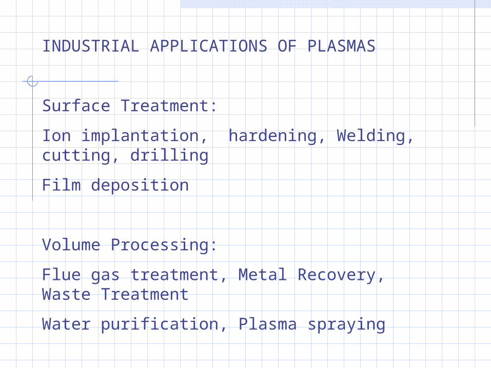
INDUSTRIAL APPLICATIONS OF PLASMAS
Surface Treatment:
Ion implantation, hardening, Welding, cutting, drilling
Film deposition
Volume Processing:
Flue gas treatment, Metal Recovery, Waste Treatment
Water purification, Plasma spraying

Light Sources
High Intensity, Discharge Lamps, Low Pressure Lamps, Specialty Sources,
Lasers, Field-Emitter Arrays, Plasma Displays
Switches:
Electric Power, Pulsed Power

Energy Converters:
MHD Generators, Thermionic Energy Converters, Beam Sources
Radiation Processing:
Ceramic powders, Plant growth
Medicine:
Surface treatment, Instrument Sterilization

MAJOR APPLICATIONS
Plasma SourcesBeamsPulsed Power TechnologyAtmospheric Pressure DischargePlasma Etching

PLASMA SOURCES
HeliconsECRsICPsMagnetronsGyrotronsThrustersGEC reference reactors
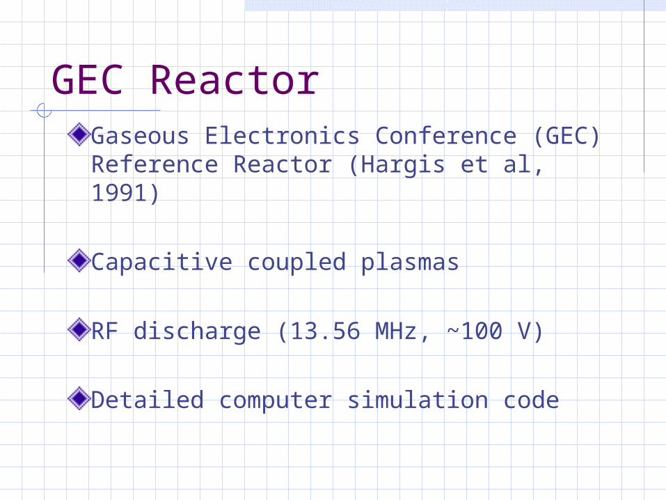
GEC ReactorGaseous Electronics Conference (GEC) Reference Reactor (Hargis et al, 1991)
Capacitive coupled plasmas
RF discharge (13.56 MHz, ~100 V)
Detailed computer simulation code

GEC Reactor: Basic parameters
Rc = 5 cm
Rr = Ra = 5.25 cm
RT = 10 cm
Xc = Xr = 3.5 cm
Xa = 6.25 cm
XT = 10 cm
d = Xa-Xc = 2.75 cm


BEAMS
Laser beamsIon beamsElectron beamsEnergetic particle beams

Ion beams:Plasma focusing
Off–focus of charged particle beams
Plasma focusing

Applications to microelectronics
“ Nano” microelectronics: Quantum Ge/Si dots Growth by molecular beams + electron
beam evaporators for Si and Ge deposition
Enhancement by ion implantation Low energy As+ beam (1 keV) Depositing current density 0.02 A/cm2

PULSED POWER TECH
Pulsed voltage
Pulsed beams

Experiments atMaterials Modification Lab,
DUT
C on Al surfaceBombarded by pulsed electron beamsRegular deposition thickness: msAfter a single pulse: ~ 1mmMulti-pulses: Better results
Anomalous diffusion effect ?

Experiments at MMLab:Pulsed electron beam
parameters
Width: ~ mPower: 27.8 keVEnergy density: 3.2 J/cm2
1. Cathode, 2. Anode, 3. Target, 4. Vacuum chamber, 5. Cathode plasma, 6. Anode plasma, 7. Coils, 8. Sparks

ATMOSHERIC DISCHARGESArc discharges Circuit breakers Plasma guns & furnaces for steel, auto and
environment industries Surface physical simulation of re-entry
Corona discharges Environment industry
Glow discharges Filament glow discharges OAUGD

Physical simulation of re-entry
Fluid model (electrostatic MHD)
Kink instabilities
Two stream instabilities
Numerical simulation codes
DUSTY PLASMA APPLICATIONS
Dust particles in reactors
Removal by heart-beating waves
Removal by bipolar diffusions
Other applications

Dust particles in reactors:Particle creations
Particle creation & growth phases
Cluster formation Nucleation and cluster growth Coagulation Particle growth


Particle creations :Major processes
Surface processes: Etching Sputtering
PECVD processes: Walls Chemical polymers
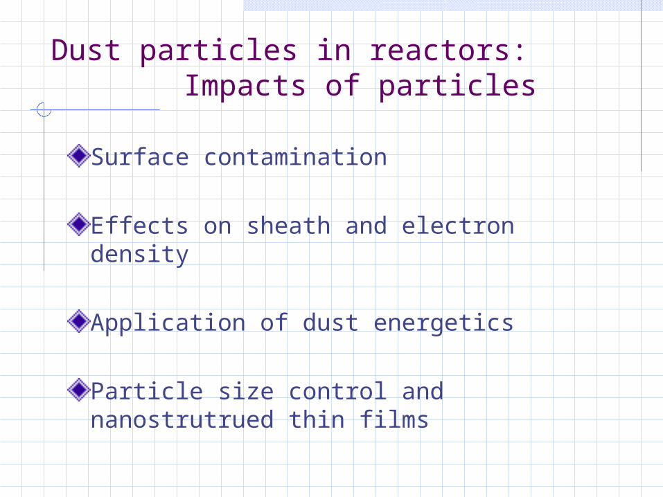
Dust particles in reactors:Impacts of particles
Surface contamination
Effects on sheath and electron density
Application of dust energetics
Particle size control and nanostrutrued thin films

Surface contamination
Particle emission and trapping in plasma processing reactors
ICPs
CCPs
Helicons and ECRs


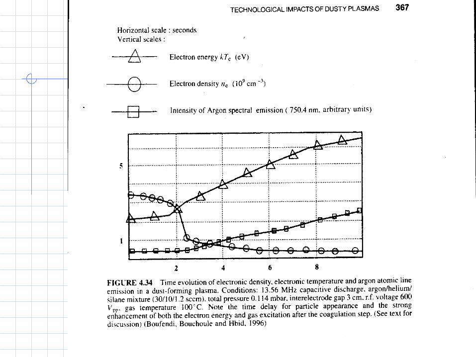
Effects on sheath and electron density
Energy absorption
Electron density reduction

Dust-free processing
Dust cleaning (removal) techniques
Magnetization and E X B drift
Dust trajectory calculations
Electrical potential configurations

Application of dust energetics
Dust energetics
Heavy particle deposition
“Dust-enhanced” PECVD
Dust charging and distribution studies
Dust size control and nanostructured thin films
Opto-electronics applications of nano-structure thin films
Nano-crystallite with dusty plasma technology

BIOPHYSICAL APPLICATIONS
Electroporation Drug delivery and gene therapy Seed modification (ion & plasma beams) ?
Surface sterilization Anti-bioterrorism application Medical and other industry applications
Surface modification To artificial organs etc.
High power, low duty circle pulses Applications to biological systems

Electroporation:Basic processes
Applying short electrical pulsesCharging of lipid bilayer membranesFast local structure rearrangementTransition to “pore” stageTremendous enhancement of ionic and molecular transport
Possible candidate for seed modification?

Electroporation:Basic parameters
Pulse width: ~ s – msPore creation period: ~ s Pore relaxation time: > 1 sPore radii: ~ nmBilayer thickness: ~ mMembrane voltage: > 1 VElectrical field: ~ kV/cm

Surface sterilization: Anti-bioterrorism application
Large scale anthrax outbreak Soviet Union, 1979 (Science 266, 1994) USA, 2001
Plasma sterilization for large areas No damage to the surface Fast cleanup: > 10cm/s In-place agent destruction, no hazard waste
Tools Montec steam plasma torch TTU arc-jet thruster

Surface sterilization: Plasma parameters
Power: 60 – 100 kWWork plasma: Water steam &Temperature: > 1500 KThreshold: > 3000 KRate > 10 cm/sKill rate: > 80 %
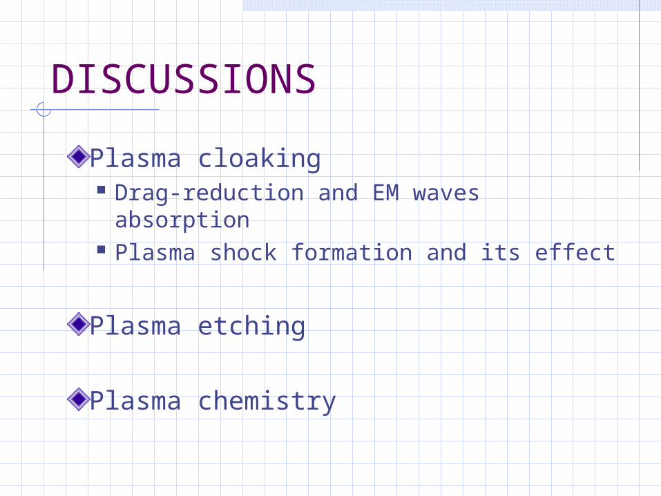
DISCUSSIONS
Plasma cloaking Drag-reduction and EM waves
absorption Plasma shock formation and its effect
Plasma etching
Plasma chemistry

University Research Centers in US
UW-UM Center for Plasma Aided Manufacturing
Research Areas:
Thin Film Deposition Thick Film Deposition Plasma Etching Surface Modification

Thin Film Deposition
Plasma-mediated, surface modification of organic and inorganic polymeric substrates for generating controlled etching reactions, creating specific surface topographies, and implanting specific functionalities onto various substrate surfaces.

Deposition of novel and conventional macromolecular layers (e.g. Teflon-like thin layers and IR transparent films) on inorganic and organic surfaces by involving plasma-state and plasma-induced reaction mechanisms, including template polymerization reaction mechanisms initiated from surfaces with plasma-enhanced crystallynity.
Investigation of the influence of plasma parameters (electron energy distribution, power, frequency, pressure, etc.) on the discharge-induced gas phase molecular fragmentation and surface-mediated plasma-chemistry mechanisms

•Kinetic modeling of plasma-induced gas phase fragmentation and gas phase and surface-mediated recombination processes (e.g. Kinetic modeling of ammonia and hydrazine-RF plasma environments).
•Generation of intelligent substrates for molecular recognition and molecular machining processes by immobilizing and synthesizing active biomolecules (e.g. enzymes, oligonucleotides) on plasma-functionalized substrate surfaces
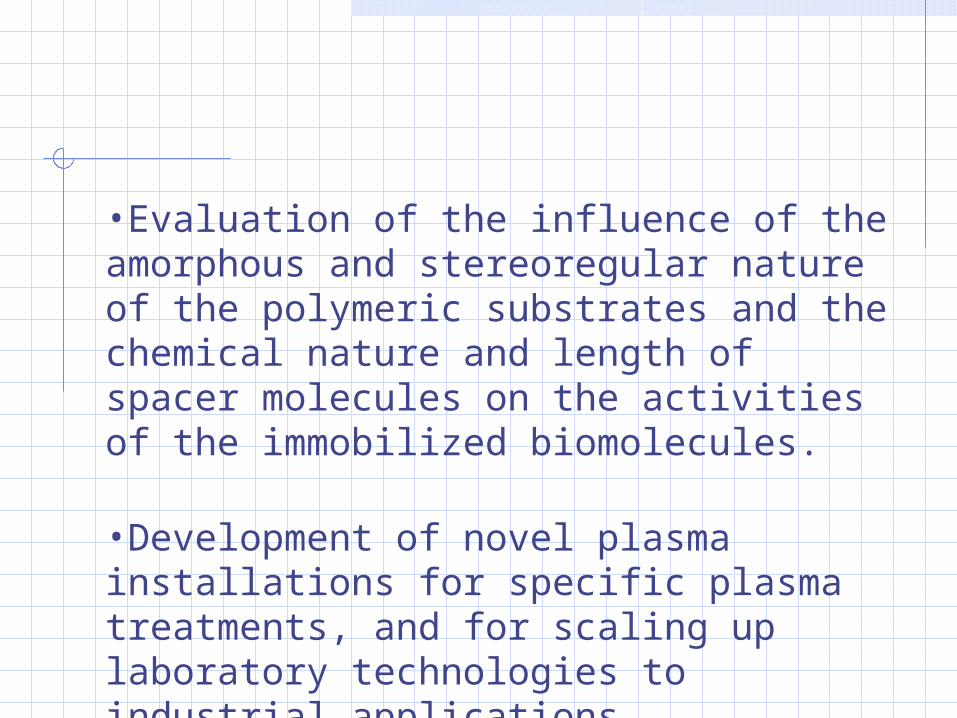
•Evaluation of the influence of the amorphous and stereoregular nature of the polymeric substrates and the chemical nature and length of spacer molecules on the activities of the immobilized biomolecules.
•Development of novel plasma installations for specific plasma treatments, and for scaling up laboratory technologies to industrial applications

Thick Film Deposition
A) Plasma spraying:
* Nozzle and shroud development and evaluation for increased plasma jet stability, and improved deposition efficiency and consistency of coating quality.
* Development of sensors and control algorithms for detecting and avoiding variations in plasma jet behavior and coating quality.

B) Wire arc spraying:
•* Spray pattern control through different nozzle and shroud designs.
•* Development of fundamental process correlations using process models andadvanced diagnostics with a novel torch.
•* Application of novel control algorithm based on computer analysis of arcvoltage traces.

•C) Thermal plasma CVD:
•* Texture control during high rate diamond film deposition through detailed understanding of the boundary layer chemistry based on modeling and diagnostics using gas chromatography.
•* Arcjet deposition at high rates of hard, boron containing films.

Plasma Etching
Etch Tool Development
Helicon plasma etching
Magnetically enhanced inductively coupled plasmas (ICP)
Large area substrates
Modeling

Semiconductor Processing:
* Fluorocarbon-based SiO2 etching - chemical characterization of gas phase using infrared spectroscopy, endpoint detection, etch selectivity/ion energy control at the wafer surface
* Plasma-Induced Damage - surface charging effects in device damage and feature profile evolution, discharge modulation for reduction of charging-induced damage, vacuum ultraviolet radiation damage
* Real-time Control of Plasma Etching - efforts includes development of sensors (e.g., wall deposition monitor), and control strategies

Advanced Plasma Etch Diagnostics
Diagnostics currently under development:
Langmuir probe theory in magnetized plasmas
Infrared absorption spectroscopy
Electro-optical probe

Recent collaborations with industrial partners
•Process development for polymer etching
•Surface charging reduction during plasma etching
•Process development for etching of magnetic materials
•Chemical characterization of plasmas for fluorocarbon-based etching of SiO2

Thank you!