Embed Size (px)
Citation preview
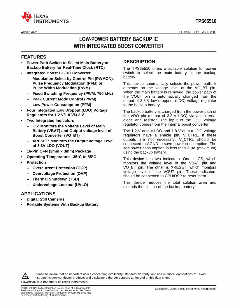
1FEATURESDESCRIPTION
APPLICATIONS
TPS65510
www.ti.com .......................................................................................................................................................................................... SLLS917–SEPTEMBER 2008
LOW-POWER BATTERY BACKUP ICWITH INTEGRATED BOOST CONVERTER
2• Power-Path Switch to Select Main Battery orBackup Battery for Real-Time Clock (RTC) The TPS65510 offers a suitable solution for power
switch to select the main battery or the backup• Integrated Boost DC/DC Converterbattery.– Modulation Select by Control Pin (PWMON),
Pulse Frequency Modulation (PFM) or This device automatically selects the power path. Itdepends on the voltage level of the VO_BT pin.Pulse Width Modulation (PWM)When the main battery is removed, the power path of– Fixed Switching Frequency (PWM, 750 kHz)the VOUT pin is automatically changed from the
– Peak Current Mode Control (PWM) output of 3.3-V low droppout (LDO) voltage regulator– Low Power Consumption (PFM) to the backup battery.
• Four Integrated Low Dropout (LDO) Voltage The backup battery is charged from the power path ofRegulators for 1.2 V/1.8 V/3.3 V the VRO pin (output of 3.3-V LDO) via an external
diode and resistor. The input of the LDO voltage• Two Integrated Indicatorsregulator comes from the internal boost converter.– CS: Monitors the Voltage Level of Main
Battery (VBAT) and Output voltage level of The 1.2-V output LDO and 1.8-V output LDO voltageregulators have a enable pin, V_CTRL. If theseBoost Converter (VO_BT)outputs are not necessary, V_CTRL should be– XRESET: Monitors the Output voltage Levelconnected to AGND to save power consumption. Theof 3.3V LDO (VOUT) self-power consumption is less than 3 µA (maximum)
• 16-Pin QFN (3mm × 3mm) Package using the backup battery.• Operating Temperature –35°C to 85°C This device has two indicators. One is CS, which• Protection monitors the voltage level of the VBAT pin and
VO_BT pin. The other is XRESET, which monitors– Overcurrent Protection (OCP)voltage level of the VOUT pin. These indicators– Overvoltage Protection (OVP) should be connected to CPU/DSP to reset them.
– Thermal Shutdown (TSD)This device reduces the total solution area and– Undervoltage Lockout (UVLO) extends the lifetime of the backup battery.
• Digital Still Cameras• Portable Systems With Backup Battery
1
Please be aware that an important notice concerning availability, standard warranty, and use in critical applications of TexasInstruments semiconductor products and disclaimers thereto appears at the end of this data sheet.
2PowerPAD is a trademark of Texas Instruments.
PRODUCTION DATA information is current as of publication date. Copyright © 2008, Texas Instruments IncorporatedProducts conform to specifications per the terms of the TexasInstruments standard warranty. Production processing does notnecessarily include testing of all parameters.

APPLICATION CIRCUIT
TPS65510
SLLS917–SEPTEMBER 2008 .......................................................................................................................................................................................... www.ti.com
These devices have limited built-in ESD protection. The leads should be shorted together or the device placed in conductive foamduring storage or handling to prevent electrostatic damage to the MOS gates.
Figure 1. Typical Application Circuit (1.2-V/1.8-V Output)
Figure 2. Typical Application Circuit (3.3-V Output)
2 Submit Documentation Feedback Copyright © 2008, Texas Instruments Incorporated
Product Folder Link(s): TPS65510

ABSOLUTE MAXIMUM RATINGS (1)
DISSIPATION RATINGS
RECOMMENDED OPERATING CONDITIONS
TPS65510
www.ti.com .......................................................................................................................................................................................... SLLS917–SEPTEMBER 2008
ORDERING INFORMATIONTA PACKAGE MARKING PACKAGE PART NUMBER
–35°C to 85°C CGK 16-pin QFN TPS65510RGT
over operating free-air temperature range (unless otherwise noted)
MIN MAX UNITVBAT, VBK –0.3 6SW –0.3 7
Input voltage range VFB, FBG –0.3 6PWMON, –0.3 6V_CTRLXRESET, CS –0.3 6
VVRO, VOUT, Output voltage range –0.3 3.6VO1R8, VO1R2VO_BT –0.3 6 VSW Switch current 1.3 A
Maximum junction temperature range 125 °CStorage temperature range –40 150 °C
(1) Stresses beyond those listed under "absolute maximum ratings" may cause permanent damage to the device. These are stress ratingsonly and functional operation of the device at these or any other conditions beyond those indicated under "recommended operatingconditions" is not implied. Exposure to absolute-maximum-rated conditions for extended periods may affect device reliability.
POWER RATING POWER RATINGPACKAGE RθJA(1)
TA < 25°C TA = 85°CQFN 47.4°C/W 2.11 W 0.844 W
(1) The thermal resistance, RθJA, is based on a soldered PowerPAD™ on 2S2P JEDEC board using thermal vias.
over operating free-air temperature range (unless otherwise noted)
MIN TYP MAX UNITVBAT 2.65 5.5
Supply voltage VVBK 1.8 5.5
High-level digital input voltage at PWMON 1.4 5.5VIH V
High-level digital input voltage at V_CTRL 1.4 VOUTLow-level digital input voltage at PWMON 0.4
VIL VLow-level digital input voltage at V_CTRL 0.4Operating free-air temperature range –35 85 °C
Copyright © 2008, Texas Instruments Incorporated Submit Documentation Feedback 3
Product Folder Link(s): TPS65510
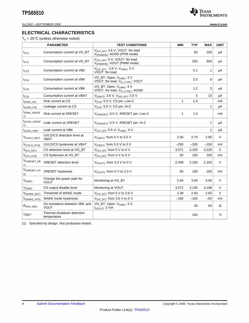
ELECTRICAL CHARACTERISTICS
TPS65510
SLLS917–SEPTEMBER 2008 .......................................................................................................................................................................................... www.ti.com
TA = 25°C (unless otherwise noted)
PARAMETER TEST CONDITIONS MIN TYP MAX UNITV(VO_BT): 3.6 V, VOUT: No loadICC1 Consumption current at VO_BT 60 100 µAV(PWMON): AGND (PFM mode)V(VO_BT): 5 V, VOUT: No loadICC2 Consumption current at VO_BT 250 350 µAV(PWMON): VOUT (PWM mode)V(VO_BT) : 3.6 V, V(VBK): 3 VICC3 Consumption current at VBK 0.1 1 µAVOUT: No loadVO_BT: Open, V(VBK): 3 VICC4 Consumption current at VBK 2.5 5 µAVOUT: No load, V(V_CTRL): VOUTVO_BT: Open, V(VBK): 3 VICC5 Consumption current at VBK 1.2 3 µAVOUT: No load, V(V_CTRL): AGND
ICC6 Consumption current at VBAT V(VBAT): 3.6 V, V(VO_BT): 3.5 V 5 10 µAI(SINK_CS) Sink current at CS V(CS): 0.5 V, CS pin: Low-Z 1 1.5 mAI(LEAK_CS) Leakage current at CS V(CS): 5.5 V, CS pin: Hi-Z 1 µAI(SINK_XRESE Sink current at XRESET V(XRESET): 0.5 V, XRESET pin: Low-Z 1 1.5 mAT)
I(LEAK_XRESE Leak current at XRESET V(XRESET): 5.5 V, XRESET pin: Hi-Z 1 µAT)
I(LEAK_VBK) Leak current at VBK V(VO_BT): 5.5 V, V(VBK): 0 V 1 µAUVLO/CS detection level atV(UVLO_DET) V(VBAT): from 0 V to 5.5 V 2.50 2.70 2.90 VVBAT
V(UVLO_HYS) UVLO/CS hysteresis at VBAT V(VBAT): from 5.5 V to 0 V –250 –200 –150 mVV(CS_DET) CS detection level at VO_BT V(VO_BT): from 5 V to 0 V 3.071 3.150 3.229 VV(CS_HYS) CS hysteresis at VO_BT V(VO_BT): from 0 V to 5 V 50 100 150 mVV(XRESET_DE XRESET detection level V(VOUT): from 3.3 V to 0 V 2.048 2.100 2.153 VT)
V(XRESET_HY XRESET hysteresis V(VOUT): from 0 V to 3.3 V 50 100 150 mVS)
Change the power path forV(SW1) Monitoring at VO_BT 2.94 3.00 3.06 VVOUTV(SW2) CS output disable level Monitoring at VOUT 3.072 3.135 3.198 VV(WAKE_DET) Threshold of WAKE mode V(VO_BT): from 0 V to 3.6 V 2.38 2.50 2.63 VV(WAKE_HYS) WAKE mode hysteresis V(VO_BT): from 3.6 V to 0 V –150 –100 –50 mV
On resistance between VBK and VO_BT: Open, V(VBK): 3 V,R(ON_VBK) 30 60 ΩVOUT I(VOUT): 2 mAThermal shutdown detectionTSD (1) 150 °Ctemperature
(1) Specified by design. Not production tested.
4 Submit Documentation Feedback Copyright © 2008, Texas Instruments Incorporated
Product Folder Link(s): TPS65510

SWITCHING CHARACTERISTICS
TPS65510
www.ti.com .......................................................................................................................................................................................... SLLS917–SEPTEMBER 2008
ELECTRICAL CHARACTERISTICS (continued)TA = 25°C (unless otherwise noted)
PARAMETER TEST CONDITIONS MIN TYP MAX UNITBoost DC/DC Converter
V(PWMON): AGND (PFM mode) 1.213 1.250 1.288V(FB) Reference voltage V
V(PWMON): VOUT (PWM mode) 1.225 1.250 1.275Overvoltage protection threshold Monitoring at FB 1.30 1.35 1.40 V
V(PWMON): AGND (PFM mode) 0.48 0.60 0.72Overcurrent protection threshold A
V(PWMON): VOUT (PWM mode) 0.8 1.0 1.2OSC Internal OSC frequency V(PWMON): VOUT (PWM mode) 675 750 825 kHzR(ON_P) P-ch FET ON resistance V(VO_BT): 5 V 500 700 mΩR(ON_N) N-ch FET ON resistance V(VO_BT): 5 V 200 250 mΩR(ON_FBG) FBG ON resistance V(PWMON): VOUT (PWM mode) 1 1.5 kΩI(LEAK_FBG) Leakage current at FBG V(PWMON): AGND (PFM mode) 1 µA3.3-V Output LDO (VOUT)V(VOUT) Output voltage of VOUT V(VO_BT): 5 V, I(VOUT): 1 mA 3.234 3.300 3.366 VI(VOUT) Output current of VOUT V(VO_BT): 5 V, V(VOUT) ≥ 3.156 V 30 mA
Overcurrent protection threshold 50 mA3.3-V Output LDO (VRO)V(VRO) Output voltage of VRO V(VO_BT): 5 V, I(VRO): 1 mA 3.234 3.300 3.366 VI(VRO) Output current of VRO V(VO_BT): 5 V, V(VRO) ≥ 3.156 V 10 30 mA
Overcurrent protection threshold 50 mA1.8-V Output LDO (VO1R8)V(VO1R8) Output voltage of VO1R8 V(V_CTRL): VOUT, V(VO_BT): 5 V, I(VO1R8): 100 µA 1.71 1.80 1.89 VI(VO1R8) Output current of VO1R8 V(V_CTRL): VOUT 100 µA1.2-V Output LDO (VO1R2)V(VO1R2) Output voltage of VO1R2 V(V_CTRL): VOUT, V(VO_BT): 5 V, I(VO1R2): 100 µA 1.1 1.2 1.3 VI(VO1R2) Output current of VO1R2 V(V_CTRL): VOUT 100 µA
TA = 25°C (unless otherwise noted)
PARAMETER TEST CONDITIONS MIN TYP MAX UNITTCS
(1) Detection delay at CS V(VO_BT): from 3.6 V to 2.0 V 55 µsTXRESET
(1) Detection delay at XRESET V(VOUT): from 1.5 V to 3.0 V 25 µs
(1) Specified by design. Not production tested.
Copyright © 2008, Texas Instruments Incorporated Submit Documentation Feedback 5
Product Folder Link(s): TPS65510

TPS65510
SLLS917–SEPTEMBER 2008 .......................................................................................................................................................................................... www.ti.com
Figure 3. Block Diagram
6 Submit Documentation Feedback Copyright © 2008, Texas Instruments Incorporated
Product Folder Link(s): TPS65510

PIN ASSIGNMENTS
TPS65510
www.ti.com .......................................................................................................................................................................................... SLLS917–SEPTEMBER 2008
TERMINAL FUNCTIONSTERMINAL
I/O (1) DESCRIPTIONNO. NAME
Boost converter output. This voltage is defined by the ration of external resistors. Please see1 VO_BT O the description in detail.Switching terminal for boost converter. This terminal should be connected to the external2 SW I inductor.
3 PGND G Power ground. Connect to the ground plane.4 AGND G Analog ground. Connect to the ground lane.
LDO Enable/Disable input. When the input level is Low, it disables the operation of LDOs5 V_CTRL I regarding VO1R8 and VO1R2. When the input level is high, it enables the operation of LDOs
regarding VO1R8 and VO1R2.Modulation select pin. When the input level is low, the boost converter operates as PFM6 PWMON I mode. When the input level is high, the boost converter operates as PWM mode.Indicator which monitors VBAT pin and VO_BT pin. CS is an open-drain output that goes low
7 CS O when the voltage level of VO_BT pin or VBAT pin is lower than the threshold. The thresholdis specified with the Electrical Characteristics.Indicator that monitors VOUT; the output of 3.3-V LDO or backup battery. XRESET is an
8 XRESET O open-drain output that goes low when the voltage level of VOUT is lower than the threshold.The threshold is specified with the Electrical Characteristics.
9 VO1R2 O 1.2-V output regulated by LDO. The voltage level sets 1.2 V internally.10 VO1R8 O 1.8-V output regulated by LDO. The voltage level sets 1.8 V internally.
3.3-V output regulated by LDO or the voltage from backup battery. This output is selected by11 VOUT O internal power switch. The selection depends on the output voltage of boost converter.12 VRO O 3.3-V output regulated by LDO. The voltage level sets 3.3 V internally.13 VBK I Backup battery input. The recommended input voltage at VBK is from 1.8V to 5.5V.
Boost converter output adjustable pin. When the level of PWMON pin is low, the impedance14 FBG I of FBG is high impedance. When the level of PWMON pin is high, the impedance of FBG is
almost GND level.15 FB I Feedback voltage from boost converter output.
Power supply from main battery. The recommended input voltage at VBAT is from 2.65V to16 VBAT I 5.5V.
(1) I: Input pin, O: Output pin, P: Power supply pin, G: GND pin
Copyright © 2008, Texas Instruments Incorporated Submit Documentation Feedback 7
Product Folder Link(s): TPS65510

TPS65510
SLLS917–SEPTEMBER 2008 .......................................................................................................................................................................................... www.ti.com
I/O Equivalent CircuitsVBAT/VO_BT CS/XRESET
V_CTRL PWMON
FB FBG
SW VOUT
8 Submit Documentation Feedback Copyright © 2008, Texas Instruments Incorporated
Product Folder Link(s): TPS65510

TPS65510
www.ti.com .......................................................................................................................................................................................... SLLS917–SEPTEMBER 2008
I/O Equivalent Circuits (continued)VO1R2 VO1R8
VBK VRO
Figure 4. I/O Equivalent Circuits
Copyright © 2008, Texas Instruments Incorporated Submit Documentation Feedback 9
Product Folder Link(s): TPS65510

FUNCTIONAL DESCRIPTION
Power-Path Switch
Boost Converter
TPS65510
SLLS917–SEPTEMBER 2008 .......................................................................................................................................................................................... www.ti.com
The TPS65510 has the switch to select a power path of VOUT pin from main battery or backup battery. Theseswitches consist of P-ch MOSFET. Also, these switches avoid the reverse current from output side to batteryside.
When the voltage of VO_BT pin (output of boost converter) is higher than the threshold specified by V(SW1) inElectrical Characteristics, the power path of VOUT comes from main battery via internal boost converter. Thevoltage of VOUT pin sets 3.3 V with internal LDO.
When a voltage of VO_BT pin is lower than the threshold specified by V(SW1) in Electrical Characteristics, thepower path of VOUT comes from backup battery at VBK pin. Before the voltage of VO_BT pin reaches V(SW1),the switch to select a power path cannot change the power path route.
The voltage coming from backup battery is not regulated internally. When the voltage of VOUT is lower than thethreshold specified by V (XRESET_DET) and V (XRESET_HYS) in Electrical Characteristics, the voltage of XRESET pingoes low (see the description of STATUS INDICATORS).
At the start of boost converter operation, the power path is different to avoid the power supply from backupbattery. In this situation, the power path of VOUT comes from main battery via internal boost converter even ifthe output voltage of VO_BT is lower than threshold for CS signal specified by V(sw1) in Electrical Characteristics.
The TPS65510 has the boost converter, and the power path comes from the main battery. It has four operationmodes, WAKE mode, Pulse Frequency Modulation (PFM) mode, Pulse Width Modulation (PWM) mode andTHROUGH mode.
At first, this converter operates as WAKE mode until the voltage of VO_BT pin is less than the thresholdspecified by V(WAKE_DET) and V(WAKE_HYS) in Electrical Characteristics. The switching frequency of WAKE mode isfixed. Only N-ch MOSFET operates during WAKE mode until the voltage of VO_BT pin reaches the thresholdspecified by V(WAKE_DET) and V(WAKE_HYS) in Electrical Characteristics.
After the voltage of VO_BT pin reaching more than the threshold specified by V(WAKE_DET) and V(WAKE_HYS) inElectrical Characteristics, the operation mode is shifted from WAKE mode to other modes selected by the level ofPWMON pin. When the voltage of PWMON pin is low level, the boost converter operates as PFM mode. Whenthe voltage of PWMON pin is high level, the boost converter operates as PWM mode. When the voltage of mainbattery is higher than the voltage of VO_BT pin, the converter operates as THROUGH mode to reduce theconsumption current at VO_BT pin. At this mode, The TPS65510 forces P-ch MOSFET to be ON and N-chMOSFET to be OFF. It means that the voltage of VO_BT pin is not regulated.
The boost converter has the reversed current protection to monitor the different voltage between VO_BT pin andSW pin. The protection monitors the difference at both PFM mode and PWM mode. When the voltage of SW pinis larger than that of VO_BT pin, the protection is activated. When the protection is activated, the internal P-chMOSFET turns OFF. This means that the voltage of SW pin converges the battery voltage naturally.
The output voltage of boost converter depends on the operation mode. When the boost converter operates asPFM mode, the impedance of FBG pin goes Hi-Z and the output voltage is defined by R1, R2 and R3 shown inFigure 1 and Figure 2. When the boost converter operates as PWM mode, the impedance of FBG pin goesalmost zero and the output voltage is defined by R1 and R2 shown in Figure 1 and Figure 2. The output voltageis calculated by Equation 1 and Equation 2.
10 Submit Documentation Feedback Copyright © 2008, Texas Instruments Incorporated
Product Folder Link(s): TPS65510

1VO_BT = FB
RV 1 + •V
æ öç ÷è øR + R2 3 (1)
1VO_BT = FB
2
RV 1 + •V
R
æ öç ÷è ø (2)
LDO Voltage Regulators
Status Indicators
TPS65510
www.ti.com .......................................................................................................................................................................................... SLLS917–SEPTEMBER 2008
PFM mode:
PWM mode:
Where:VVO_BT: Voltage of VO_BT pin
VFB: Voltage of FBpin defined byreference voltage inElectricalCharacteristics
The TPS65510 has four types of LDO voltage regulators; 1.2-V output (LDO1, shown in Figure 3), 1.8-V output(LDO2, shown in Figure 3) and 3.3-V dual output (LDO3 and LDO4, shown in Figure 3). These output voltageare set by internal feedback loop only. The device has enable/disable control pin named V_CTRL for LDO1 andLDO2. When the voltage of V_CTRL is low level, the device disables the output of LDO1 and LDO2. When thevoltage of V_CTRL is high level, the device enables the output of LDO1 and LDO2.
The power paths of LDO2, LDO3, and LDO4 are fixed; from output of LDO3 for LDO2 and from output of boostconverter for LDO3 and LDO4. The power path of LDO1 is selected by power path switch; when output voltageof the boost converter is higher than the threshold specified by V(SW1) in Electrical Characteristics, the pathcomes from output of LDO4. When output voltage of the boost converter is lower than the threshold specified byV(SW1) in Electrical Characteristics, the path comes from backup battery connected to VBK pin.
The maximum outputs current are specified by I(VO1R2), I(VO1R8), I(VRO) and I(VOUT) in Electrical Characteristics.
The TPS65510 has two device status indicators; CS and XRESET. These signal pins consist of open drain ofN-ch MOSFET. Due to this, the pullup resistors should be needed. The recommended values of pullup resistorsare 100 kΩ.
CS function monitors the voltage level of VBAT pin and VO_BT pin for selecting power path of VOUT. When thesignal level of CS pin is high level, the power path of VOUT comes from the main battery via the boost converter.When the signal level of CS pin is low level, it comes from backup battery except the starting operation of boostconverter. When the boost converter starts operation with the main battery, the P-ch MOSFET at LDO4 turns ONto avoid supplying the power from backup battery even if the voltage of VOUT is lower than the thresholdspecified by V(SW1) in Electrical Characteristics. The signal of the CS pin remains low level when the main batteryis removed (including the transition) or the voltage level of VOUT does not achieve the threshold specified byV(SW2) in Electrical Characteristics.
XRESET function monitors the voltage level of VOUT pin for resetting the load like RTC. When the voltage ofVOUT is more than the threshold specified by V(XRESET_DET) and V(XRESET_HYS) in Electrical Characteristics, thesignal level of XRESET pin is high. When the voltage of VOUT is less than the threshold specified byV(XRESET_DET) and V(XRESET_HYS) in Electrical Characteristics, the signal level of XRESET pin is low. This situationrequires resetting the load. The detailed waveform is shown in Figure 5.
Copyright © 2008, Texas Instruments Incorporated Submit Documentation Feedback 11
Product Folder Link(s): TPS65510

TPS65510
SLLS917–SEPTEMBER 2008 .......................................................................................................................................................................................... www.ti.com
Summary of Status Indicator and Power-Path SwitchDescription
Detection Voltage of VO_BT pinCS (1)
Detect level V(CS_DET) and V(CS_HYS) in Electrical CharacteristicsDetection Voltage of VOUT pinDisable
CS signal Detect level V(SW2) in Electrical CharacteristicsDetection Voltage of VOUT pin
XRESETDetect level V(XRESET_DET) and V(XRESET_HYS) in Electrical CharacteristicsDetection of Voltage of VO_BT pinpath changePower SW (2)
Detect level V(SW1) in Electrical Characteristics
(1) When the voltage of VBAT pin is less than the threshold of UVLO, the output of CS pin forces low level.(2) The Power path switch changes the path after the voltage of VO_BT is higher than V(CS_DET). Before that, the power path of VOUT
comes from VO_BT pin; not VBK pin.
12 Submit Documentation Feedback Copyright © 2008, Texas Instruments Incorporated
Product Folder Link(s): TPS65510

TPS65510
www.ti.com .......................................................................................................................................................................................... SLLS917–SEPTEMBER 2008
Figure 5. Power-Path Switch Timing Chart
Copyright © 2008, Texas Instruments Incorporated Submit Documentation Feedback 13
Product Folder Link(s): TPS65510

Protection
TPS65510
SLLS917–SEPTEMBER 2008 .......................................................................................................................................................................................... www.ti.com
The TPS65510 has over current protection (OCP), over voltage protection (OVP) Thermal shutdown (TSD) andUnder Voltage Lock Out (UVLO). See Table 1.
Table 1. Conditions of ProtectionsPIN PROTECTION CONDITION
Detect condition Voltage of FB pin is greater than the threshold.OVP Change mode Operation disable without latch off
Recovery condition Voltage of FB pin is less than the threshold (auto recovery).Current of SW pin is greater than the threshold with counting 64 cycles × 750 [kHz] andSW Detect condition the output voltage of VO_BT is less than 85% compared with the target voltage.
OCP Change mode Operation mode changes from PWM mode to PFM mode.Current of SW pin is less than the threshold and input edge signal from low level to highRecovery condition level at the PWMON pin.
Detect condition Current of VOUT pin is greater than the threshold.VOUT OCP Change mode Operation disable without latch off
Recovery condition Current of VOUT pin is less than the threshold (auto recovery).Detect condition Current of VRO pin is greater than the threshold.
VRO OCP Change mode Operation disable without latch offRecovery condition Current of VRO pin is less than the threshold (auto recovery).Detect condition Temperature of chip is greater than the threshold.Change mode Operation of boost converter shuts down with latch off.- TSD
Temperature of chip is lower than the threshold. Connect the main battery afterRecovery condition disconnecting the main battery from the systemDetect condition Voltage of VBAT pin is less than the threshold.
VBAT UVLO Change mode Operation of boost converter shutdown without latch offRecovery condition Connect the main battery after disconnecting the main battery from the system.
14 Submit Documentation Feedback Copyright © 2008, Texas Instruments Incorporated
Product Folder Link(s): TPS65510

PACKAGE OPTION ADDENDUM
www.ti.com 10-Dec-2020
Addendum-Page 1
PACKAGING INFORMATION
Orderable Device Status(1)
Package Type PackageDrawing
Pins PackageQty
Eco Plan(2)
Lead finish/Ball material
(6)
MSL Peak Temp(3)
Op Temp (°C) Device Marking(4/5)
Samples
TPS65510RGTR ACTIVE VQFN RGT 16 3000 RoHS & Green NIPDAU Level-2-260C-1 YEAR -35 to 85 CGK
TPS65510RGTT ACTIVE VQFN RGT 16 250 RoHS & Green NIPDAU Level-2-260C-1 YEAR -35 to 85 CGK
(1) The marketing status values are defined as follows:ACTIVE: Product device recommended for new designs.LIFEBUY: TI has announced that the device will be discontinued, and a lifetime-buy period is in effect.NRND: Not recommended for new designs. Device is in production to support existing customers, but TI does not recommend using this part in a new design.PREVIEW: Device has been announced but is not in production. Samples may or may not be available.OBSOLETE: TI has discontinued the production of the device.
(2) RoHS: TI defines "RoHS" to mean semiconductor products that are compliant with the current EU RoHS requirements for all 10 RoHS substances, including the requirement that RoHS substancedo not exceed 0.1% by weight in homogeneous materials. Where designed to be soldered at high temperatures, "RoHS" products are suitable for use in specified lead-free processes. TI mayreference these types of products as "Pb-Free".RoHS Exempt: TI defines "RoHS Exempt" to mean products that contain lead but are compliant with EU RoHS pursuant to a specific EU RoHS exemption.Green: TI defines "Green" to mean the content of Chlorine (Cl) and Bromine (Br) based flame retardants meet JS709B low halogen requirements of <=1000ppm threshold. Antimony trioxide basedflame retardants must also meet the <=1000ppm threshold requirement.
(3) MSL, Peak Temp. - The Moisture Sensitivity Level rating according to the JEDEC industry standard classifications, and peak solder temperature.
(4) There may be additional marking, which relates to the logo, the lot trace code information, or the environmental category on the device.
(5) Multiple Device Markings will be inside parentheses. Only one Device Marking contained in parentheses and separated by a "~" will appear on a device. If a line is indented then it is a continuationof the previous line and the two combined represent the entire Device Marking for that device.
(6) Lead finish/Ball material - Orderable Devices may have multiple material finish options. Finish options are separated by a vertical ruled line. Lead finish/Ball material values may wrap to twolines if the finish value exceeds the maximum column width.
Important Information and Disclaimer:The information provided on this page represents TI's knowledge and belief as of the date that it is provided. TI bases its knowledge and belief on informationprovided by third parties, and makes no representation or warranty as to the accuracy of such information. Efforts are underway to better integrate information from third parties. TI has taken andcontinues to take reasonable steps to provide representative and accurate information but may not have conducted destructive testing or chemical analysis on incoming materials and chemicals.TI and TI suppliers consider certain information to be proprietary, and thus CAS numbers and other limited information may not be available for release.
In no event shall TI's liability arising out of such information exceed the total purchase price of the TI part(s) at issue in this document sold by TI to Customer on an annual basis.

PACKAGE OPTION ADDENDUM
www.ti.com 10-Dec-2020
Addendum-Page 2

TAPE AND REEL INFORMATION
*All dimensions are nominal
Device PackageType
PackageDrawing
Pins SPQ ReelDiameter
(mm)
ReelWidth
W1 (mm)
A0(mm)
B0(mm)
K0(mm)
P1(mm)
W(mm)
Pin1Quadrant
TPS65510RGTR VQFN RGT 16 3000 330.0 12.4 3.3 3.3 1.1 8.0 12.0 Q2
TPS65510RGTT VQFN RGT 16 250 180.0 12.4 3.3 3.3 1.1 8.0 12.0 Q2
PACKAGE MATERIALS INFORMATION
www.ti.com 16-Oct-2020
Pack Materials-Page 1

*All dimensions are nominal
Device Package Type Package Drawing Pins SPQ Length (mm) Width (mm) Height (mm)
TPS65510RGTR VQFN RGT 16 3000 853.0 449.0 35.0
TPS65510RGTT VQFN RGT 16 250 210.0 185.0 35.0
PACKAGE MATERIALS INFORMATION
www.ti.com 16-Oct-2020
Pack Materials-Page 2


www.ti.com
PACKAGE OUTLINE
C
16X 0.300.18
1.68 0.07
16X 0.50.3
1.00.8
(0.2) TYP
0.050.00
12X 0.5
4X1.5
A 3.12.9
B
3.12.9
VQFN - 1 mm max heightRGT0016CPLASTIC QUAD FLATPACK - NO LEAD
4222419/C 04/2021
PIN 1 INDEX AREA
0.08
SEATING PLANE
1
49
12
5 8
16 13
(OPTIONAL)PIN 1 ID 0.1 C A B
0.05
EXPOSEDTHERMAL PAD
SYMM
SYMM
NOTES: 1. All linear dimensions are in millimeters. Any dimensions in parenthesis are for reference only. Dimensioning and tolerancing per ASME Y14.5M. 2. This drawing is subject to change without notice. 3. The package thermal pad must be soldered to the printed circuit board for thermal and mechanical performance.
SCALE 3.600

www.ti.com
EXAMPLE BOARD LAYOUT
0.07 MINALL AROUND
0.07 MAXALL AROUND
16X (0.24)
16X (0.6)
( 0.2) TYPVIA
12X (0.5)
(2.8)
(2.8)
(0.58)TYP
( 1.68)
(R0.05)ALL PAD CORNERS
(0.58) TYP
VQFN - 1 mm max heightRGT0016CPLASTIC QUAD FLATPACK - NO LEAD
4222419/C 04/2021
SYMM
1
4
5 8
9
12
1316
SYMM
LAND PATTERN EXAMPLESCALE:20X
NOTES: (continued) 4. This package is designed to be soldered to a thermal pad on the board. For more information, see Texas Instruments literature number SLUA271 (www.ti.com/lit/slua271).5. Vias are optional depending on application, refer to device data sheet. If any vias are implemented, refer to their locations shown on this view. It is recommended that vias under paste be filled, plugged or tented.
SOLDER MASKOPENING
METAL UNDERSOLDER MASK
SOLDER MASKDEFINED
METAL
SOLDER MASKOPENING
SOLDER MASK DETAILS
NON SOLDER MASKDEFINED
(PREFERRED)

www.ti.com
EXAMPLE STENCIL DESIGN
16X (0.6)
16X (0.24)
12X (0.5)
(2.8)
(2.8)
( 1.55)
(R0.05) TYP
VQFN - 1 mm max heightRGT0016CPLASTIC QUAD FLATPACK - NO LEAD
4222419/C 04/2021
NOTES: (continued) 6. Laser cutting apertures with trapezoidal walls and rounded corners may offer better paste release. IPC-7525 may have alternate design recommendations.
SYMM
ALL AROUNDMETAL
SOLDER PASTE EXAMPLEBASED ON 0.125 mm THICK STENCIL
EXPOSED PAD 17:
85% PRINTED SOLDER COVERAGE BY AREA UNDER PACKAGESCALE:25X
SYMM
1
4
5 8
9
12
1316
17

IMPORTANT NOTICE AND DISCLAIMERTI PROVIDES TECHNICAL AND RELIABILITY DATA (INCLUDING DATASHEETS), DESIGN RESOURCES (INCLUDING REFERENCEDESIGNS), APPLICATION OR OTHER DESIGN ADVICE, WEB TOOLS, SAFETY INFORMATION, AND OTHER RESOURCES “AS IS”AND WITH ALL FAULTS, AND DISCLAIMS ALL WARRANTIES, EXPRESS AND IMPLIED, INCLUDING WITHOUT LIMITATION ANYIMPLIED WARRANTIES OF MERCHANTABILITY, FITNESS FOR A PARTICULAR PURPOSE OR NON-INFRINGEMENT OF THIRDPARTY INTELLECTUAL PROPERTY RIGHTS.These resources are intended for skilled developers designing with TI products. You are solely responsible for (1) selecting the appropriateTI products for your application, (2) designing, validating and testing your application, and (3) ensuring your application meets applicablestandards, and any other safety, security, or other requirements. These resources are subject to change without notice. TI grants youpermission to use these resources only for development of an application that uses the TI products described in the resource. Otherreproduction and display of these resources is prohibited. No license is granted to any other TI intellectual property right or to any third partyintellectual property right. TI disclaims responsibility for, and you will fully indemnify TI and its representatives against, any claims, damages,costs, losses, and liabilities arising out of your use of these resources.TI’s products are provided subject to TI’s Terms of Sale (https:www.ti.com/legal/termsofsale.html) or other applicable terms available eitheron ti.com or provided in conjunction with such TI products. TI’s provision of these resources does not expand or otherwise alter TI’sapplicable warranties or warranty disclaimers for TI products.IMPORTANT NOTICE
Mailing Address: Texas Instruments, Post Office Box 655303, Dallas, Texas 75265Copyright © 2021, Texas Instruments Incorporated