Embed Size (px)
Citation preview
AL8871Q 60V BUCK-BOOST LED CONTROLLER
Description
The AL8871Q is an LED driver, controller IC for driving external MOSFETs to drive high-current LEDs. The buck-boost topology controller enables it to efficiently control the current through series-connected LEDs. The 60V capability enables it to be used in a wide range of applications and drive in excess of 15 LEDs in series.
The AL8871Q is a modified hysteretic controller using a patent-pending control scheme providing high-output current accuracy. High-accuracy dimming is achieved through DC control and high-frequency PWM control.
The AL8871Q uses two pins for fault diagnosis. A flag output highlights a fault, while the multi-level status pin gives further information on the exact fault.
The AL8871Q has been qualified to AEC-Q100 Grade 1 and is automotive compliant supporting PPAPs.
Features • AEC-Q100 Grade 1 Qualified • Wide Input Voltage Range: 5V to 60V • Operating Frequency Up to 1MHz • Analog Dimming Range: 10% to 100% • 1000:1 PWM Dimming Resolution at 500 Hz • High Temperature Control of LED Current Using TCTRL • Fault Reporting for Abnormal Operations • Overtemperature Shutdown • Available in Thermally Enhanced TSSOP-16EP Package • Totally Lead-Free & Fully RoHS Compliant (Notes 1 & 2) • Halogen and Antimony Free. “Green” Device (Note 3) • PPAP Capable (Note 4)
Pin Assignments (Top View)
1
2
3 14
16CTRL
REF
NTC FAULT
GI
PWM15
4COMP 13 CSEP
5
6
STATUS
SGND
7PGND
11 BST
VIN12
10 DRV
8N/C 9 N/C
TSSOP-16EP
Applications • Automotive Daytime Running Lights • Automotive Head Lamps • Automotive Fog Lamps • Automotive Interior Lamps
Notes: 1. No purposely added lead. Fully EU Directive 2002/95/EC (RoHS), 2011/65/EU (RoHS 2) & 2015/863/EU (RoHS 3) compliant.
2. See https://www.diodes.com/quality/lead-free/ for more information about Diodes Incorporated’s definitions of Halogen- and Antimony-free, "Green" and Lead-free. 3. Halogen- and Antimony-free "Green” products are defined as those which contain <900ppm bromine, <900ppm chlorine (<1500ppm total Br + Cl) and <1000ppm antimony compounds. 4. Automotive products are AEC-Q100 qualified and are PPAP capable. Refer to https://www.diodes.com/quality/.
AL8871Q Document number: DS41547 Rev. 1 - 2
1 of 24 www.diodes.com
December 2018 © Diodes Incorporated
AL8871Q
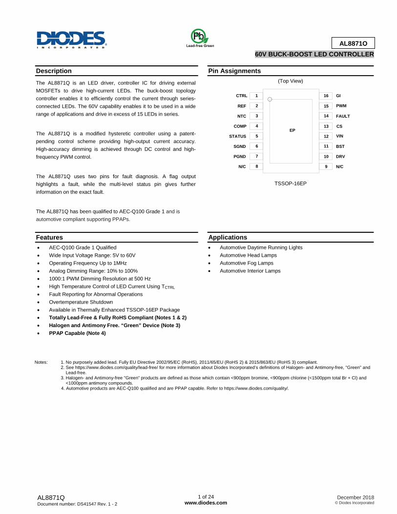
Typical Applications Circuit
AL8871Q
REF
BST
EP
CS
VIN
PGND
COMP
DRV
VIN
NTC
STATUS
CTRL
PWM
GI
FAULT
SGND
CIN
R9
R10
R1
R2
RS
L
D1
Q1
Figure 1. Typical Application Circuit
AL8871Q Document number: DS41547 Rev. 1 - 2
2 of 24 www.diodes.com
December 2018 © Diodes Incorporated

AL8871Q
Pin Descriptions
Pin Name Pin Type (Note 5) Description
CTRL 1 I
Adjust Input (for DC Output Current Control). Connect to REF to set 100% output current. Drive with DC voltage (125mV < VCTRL < 1.25V) to adjust output current from 10% to 100% of preset value. The CTRL pin has an internal clamp that limits the internal node to less than 3V, which provides some failsafe should they get overdriven.
REF 2 O Internal 1.25V Reference Voltage Output.
NTC 3 I Temperature Adjust Input for LED Thermal Current Control. Connect thermistor/resistor network to this pin to reduce output current above a preset temperature threshold. Connect to REF to disable thermal compensation function.
COMP 4 I/O Shaping Capacitor for Feedback Control Loop. Connect 330pF ±20% capacitor from this pin to ground to provide loop compensation.
STATUS 5 O
Operation Status Output (Analog Output). Pin is at 4.5V (nominal) during normal operation. Pin switches to a lower voltage to indicate specific operation warnings or fault conditions. Status pin voltage is low during shutdown mode.
SGND 6 P Signal Ground (Connect to 0V).
PGND 7 P Power Ground. Connect to 0V and pin 8 to maximize copper area.
N/C 8 — Not Connected Internally. Recommend connection to pin 7, (PGND), to maximize PCB copper for thermal dissipation.
N/C 9 — Not Connected Internally. Recommend connection pin 10 (DRV) to permit wide copper trace to gate of MOSFET.
DRV 10 O Gate Drive Output to External NMOS Transistor. Connect to Pin 9.
BST 11 P
Auxiliary Positive Supply to Internal Switch Gate Driver. At VIN < 8V; a bootstrap circuit (where applicable) is recommended to ensure adequate gate drive voltage (see Applications section). At VIN > 8V; connect to VIN. At VIN >24V; to reduce power dissipation, BST can be connected to an 8V to 15V auxiliary power supply (see Applications section). Decouple to ground with capacitor close to device (see Applications section).
VIN 12 P Input Supply to Device 5V to 60V. Decouple to ground with capacitor close to device (refer to Applications section).
CS 13 I Current Monitor Input. Connect current sense resistor between this pin and VIN. The nominal voltage, VSENSE, across the resistor initially 225mV varying with duty cycle.
FAULT 14 O Flag Open Drain Output. Pin is high impedance during normal operation. Pin switches low to indicate a fault, or warning condition.
PWM 15 I
Digital PWM Output Current Control. Pin driven either by open-drain or push-pull 3.3V or 5V logic levels. Drive with frequency higher than 100Hz to gate output on and off during dimming control. The device enters standby mode when PWM pin is driven with logic-low level for more than 15ms nominal (refer to Applications section for more details).
GI 16 I
Gain Setting Input. Used to set the device to control the sense voltage. Connect to resistive divider from CTRL to SGND. The GI divider is required to compensate for duty cycle gating in the internal feedback loop (see Applications section). The GI pin has an internal clamp that limits the internal node to less than 3V. This provides some failsafe should it become overdriven.
EP PAD P Exposed Paddle. Connect to GND plane for electrical and thermal management.
Note: 5. Type refers to whether or not pin is an input, output, input/output, or power supply pin.
AL8871Q Document number: DS41547 Rev. 1 - 2
3 of 24 www.diodes.com
December 2018 © Diodes Incorporated
AL8871Q
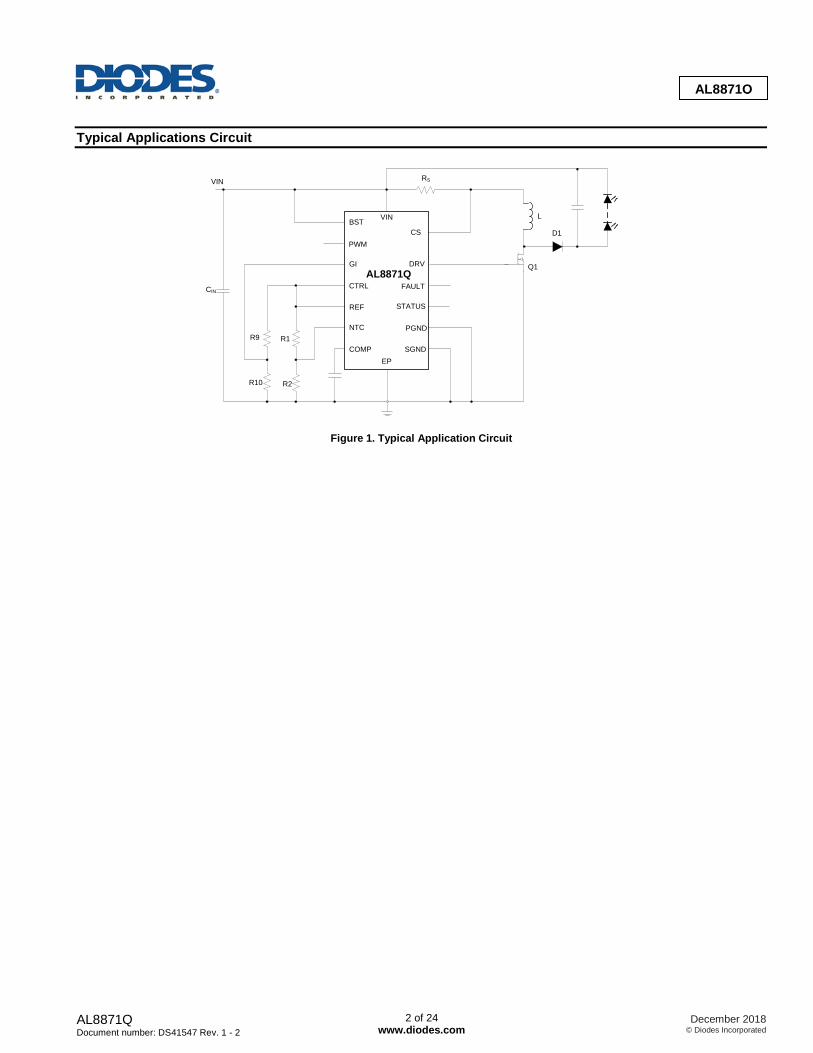
Functional Block Diagram
Fastcurrent monitor
Accurate current monitor
-Error amp
NT
Demand current source
Frequency & hysteresis
control
Gate driver
CTRL
COMP
RSVIN
+
-
LOAD
L
GI
D
R10
R9
VIN CSBST
BST
PWM
SGND PGND
REF
NTC
Reference
STATUS
FAULT
Error report
NTC
Figure 2. Functional Block Diagram
Absolute Maximum Ratings (Note 6)
Symbol Parameter Rating Unit VIN Input Supply Voltage -0.3 to 65 V
BST Auxiliary Supply Voltage -0.3 to 65 V
VCS Current Monitor Input Relative to GND -0.3 to 65 V
VSENSE Current Monitor Sense Voltage (VIN-VCS) -0.3 to 5 V
VDRV Gate Driver Output Voltage -0.3 to 20 V
IDRV Gate Driver Continuous Output Current 18 mA
VFAULT Flag Output Voltage -0.3 to 40 V
VPWM, VCTRL, VNTC, VGI, VPWM Other Input Pins -0.3 to 5.5 V
TJ Maximum Junction Temperature +150 °C
TST Storage Temperature -55 to +150 °C
Note: 6. Stresses greater than those listed under Absolute Maximum Ratings can cause permanent damage to the device. These are stress ratings only, and functional operation of the device at these or any other conditions beyond those indicated under Recommended Operating Conditions is not implied. Exposure to Absolute Maximum Ratings for extended periods can affect device reliability.
AL8871Q Document number: DS41547 Rev. 1 - 2
4 of 24 www.diodes.com
December 2018 © Diodes Incorporated
AL8871Q
ESD Ratings
Symbol Parameter Rating Unit
VESD Human Body Model (HBM) ±1500
V Charged Device Model (CDM) ±1000
Thermal Information (Note 7)
Symbol Parameter Rating Unit ϴJA Junction-to-ambient thermal resistance 50 °C/W
ϴJC Junction-to-case(top) thermal resistance 23 °C/W
Notes: 7. Measured on High Effective Thermal Conductivity Test Board according to JESD51.
Recommended Operating Conditions
Symbol Parameter Performance/Comment Min Max Unit
VIN Input Supply Voltage Range Normal Operation 8.0 60
V Reduced Performance Operation (Note 8) 5.0 8.0
VBST Auxiliary Supply Voltage Range (Note 9) Normal Operation 8.0 60
V Reduced Performance Operation (Note 8) 5.0 8.0
VSENSE Differential Input Voltage VIN-VCS, with 0 ≤ VCTRL ≤ 2.5 0 450 mV
VCTRL External DC Control Voltage Applied to CTRL pin to Adjust Output Current
DC Brightness Control Mode From 10% to 100% 0.125 1.25 V
IREF Reference External Load Current REF Sourcing Current — 1 mA fmax Recommended Switching Frequency Range (Note 10) 300 1000 kHz VNTC Temperature Adjustment (NTC) Input Voltage Range — 0 VREF V
fPWM Recommended PWM Dimming Frequency Range To Achieve 1000:1 Resolution 100 500 Hz To Achieve 500:1 Resolution 100 1000 Hz
tPWMH/L PWM Pulse Width In Dimming Mode PWM Input High or Low 0.002 10 ms VPWMH PWM Pin High Level Input Voltage — 2 5.5 V VPWML PWM Pin Low Level Input Voltage — 0 0.4 V
TJ Operating Junction Temperature Range — -40 +125 °C GI Gain Setting Ratio Ratio= VGI/VCTRL 0.20 0.50 —
Notes: 8. Device starts up above 5.4V, and as such, the minimum applied supply voltage must be above 5.4V (plus any noise margin). However, the AL8871Q continues to function when the input voltage is reduced from ≥ 8V down to 5.0V. When operating with input voltages below 8V, the output current and device parameters may deviate from their normal values and are dependent on power MOSFET switch, load, and ambient temperature conditions. To ensure best operation with input voltages, VIN, between 5V and 8V a suitable bootstrap network on BST pin is recommended.
9. BST can be driven from a voltage higher than VIN to provide higher efficiency at low VIN voltages, but to avoid false operation; a voltage must not be applied to BST in the absence of a voltage at VIN. BST can also be operated at a lower voltage than VIN to increase efficiencies at high VIN.
10. The device contains circuitry to control the switching frequency to approximately 400kHz.
AL8871Q Document number: DS41547 Rev. 1 - 2
5 of 24 www.diodes.com
December 2018 © Diodes Incorporated
AL8871Q
Electrical Characteristics (Test conditions: VIN = VBST = 12V, TA = 25°C, unless otherwise specified.)
Symbol Parameter Conditions Min Typ Max Units Supply and Reference Parameters
VUV- Undervoltage Detection Threshold Normal Operation to Switch Disabled
VIN or VBST Falling (Note 11) — 4.5 — V
VUV+ Undervoltage Detection Threshold Switch Disabled to Normal Operation
VIN or VBST Rising (Note 11) — 4.9 — V
IQ-IN Quiescent Current into VIN PWM Pin Floating Output Not Switching
— 1.5 3 mA
IQ-AUX Quiescent Current into BST — 150 300 µA
ISB-IN Standby Current into VIN PWM Pin Grounded for More Than 15ms
— 90 150 µA
ISB-AUX Standby Current into BST — 0.7 10 µA
VREF Internal Reference Voltage No Load 1.237 1.25 1.263 V
∆VREF Change in Reference Voltage with Output Current Sourcing 1mA -5 — —
mV Sinking 25µA — — 5
VREF_LINE Reference Voltage Line Regulation VIN = VBST, 8.0V<VIN = <60V -60 -90 — dB VREF-TC Reference Temperature Coefficient — — ±50 — ppm/°C
DC-DC Converter Parameters
ICTRL CTRL Input Current (Note 12) VCTRL ≤ 1.25V — — 100 nA
VCTRL = 5.0V — — 5 µA
VGI GI Voltage threshold (Note 12) VCTRL = 1.25V — — 0.8 V
IGI GI Input Current (Note 12) VGI ≤ 1.25V — — 100 nA
VGI = 5.0V — — 5 µA
IPWM PWM Input Current VPWM = 5.5V — 36 100 µA
tPWMoff PWM Pulse Width (to Enter Shutdown State) PWM Input Low 10 15 25 ms
TSDH Thermal Shutdown Upper Threshold (DRV Output Forced Low)
Temperature Rising — 150 — °C
TSDL Thermal Shutdown Lower Threshold (DRV Output Re-Enabled)
Temperature Falling — 125 — °C
High-Side Current Monitor (Pin CS) ICS Input Current Measured into CS pin VCS = 12V — 11 20 µA
VSENSE_acc Accuracy of Nominal VSENSE Threshold Voltage VCTRL = 1.25V
— ±0.25 ±2 %
VSENSE-OC Over-Current Sense Threshold Voltage 300 350 375 mV
Notes: 11. UVLO levels are such that all AL8871Q will function above 5.4V for rising supply voltages and function down to 5V for falling supply voltages. 12. The CTRL and GI pins have an internal clamp that limits the internal node to less than 3V. This provides some failsafe should those pins get overdriven.
AL8871Q Document number: DS41547 Rev. 1 - 2
6 of 24 www.diodes.com
December 2018 © Diodes Incorporated
AL8871Q
Electrical Characteristics (continued) (Test conditions: VIN = VBST = 12V, TA = +25°C, unless otherwise specified.)
Symbol Parameter Conditions Min Typ Max Units Output Parameters
VFAULTL FAULT Pin Low Level Output Voltage Output Sinking 1mA — — 0.5 V
IFAULTOFF FAULT Pin Open-Drain Leakage Current VFAULT = 40V — — 1 µA
VSTATUS STATUS Flag No-Load Output Voltage (Note 13)
Normal Operation 4.2 4.5 4.8
V
Out of Regulation (VCOMP out of range) (Note 14)
3.3 3.6 3.9
VIN Undervoltage (VIN < UVLO) 3.3 3.6 3.9
Switch Stalled (tON or tOFF > 100µs) 3.3 3.6 3.9
Overtemperature (TJ > +125°C) 1.5 1.8 2.1
Excess Sense Resistor Current (VSENSE > 0.32V)
0.6 0.9 1.2
RSTATUS Output Impedance of STATUS Output Normal Operation — 10 — kΩ
Driver Output (PIN DRV)
VDRVH High Level Output Voltage No load Sourcing 1mA (Note 15)
VIN = VBST = 12V 10 11 12 V
VDRVL Low Level Output Voltage Sinking 1mA, (Note 16) — — 0.5 V
VDRVCL High Level DRV CLAMP Voltage VIN = VAU X= VCS = 18V IDRV = 1mA
— 12.8 15 V
IDRV Dynamic Peak Current Available During Rise or Fall of Output Voltage
Charging or Discharging gate of External Switch with QG = 10nC and 400kHz
— ±300 — mA
tSTALL Time to Assert STALL Flag and Warning on STATUS Output (Note 17)
DRV Low or High — 100 170 µs
LED Thermal Control Circuit (NTC) Parameters
VNTCH Upper Threshold Voltage Onset of Output Current Reduction (VNTC Falling)
560 625 690 mV
VNTCL Lower Threshold Voltage Output Current Reduced to <10% of Set Value (VNTC Falling)
380 440 500 mV
INTC NTC Pin Input Current VNTC = 1.25V — — 1 µA
Notes: 13. In the event that more than one fault/warning condition occurs, the higher priority condition takes precedence. For example Excessive coil current and Out of regulation occurring together produces an output of 0.9V on the STATUS pin. These STATUS pin voltages apply for an input voltage to VIN of 7.5V < VIN < 60V. Below 7.5V the STATUS pin voltage levels reduce and therefore may not report the correct status. For 5.4V < VIN < 7.5V, the FAULT pin still reports any error by going low. At low VIN, an overcurrent status may be indicated when operating at high boost ratios—this is due to the feedback loop increasing the sense voltage. For more information see the Application Information section about FAULT/Status levels. 14. FAULT is asserted if VCOMP < 1.5V or VCOMP > 2.5V. 15. DRV is switched to the supply voltage VBST for low values of VBST (5V ≤VBST ≤ ~12V). For VBST > 12V, DRV is clamped internally to prevent it exceeding 15V. Below 12V, the minimum DRV pin voltage is 2.5V below VBST. 16. DRV is switched to PGND by an NMOS transistor. 17. If tON exceeds tSTALL, the device forces DRV low to turn off the external switch and then initiate a restart cycle. During this phase, CTRL is grounded internally, and the COMP pin is switched to its nominal operating voltage before operation is allowed to resume. Restart cycles are repeated automatically until the operating conditions are such that normal operation can be sustained. If tOFF exceeds tSTALL, the switch remains off until normal operation is possible.
AL8871Q Document number: DS41547 Rev. 1 - 2
7 of 24 www.diodes.com
December 2018 © Diodes Incorporated
AL8871Q
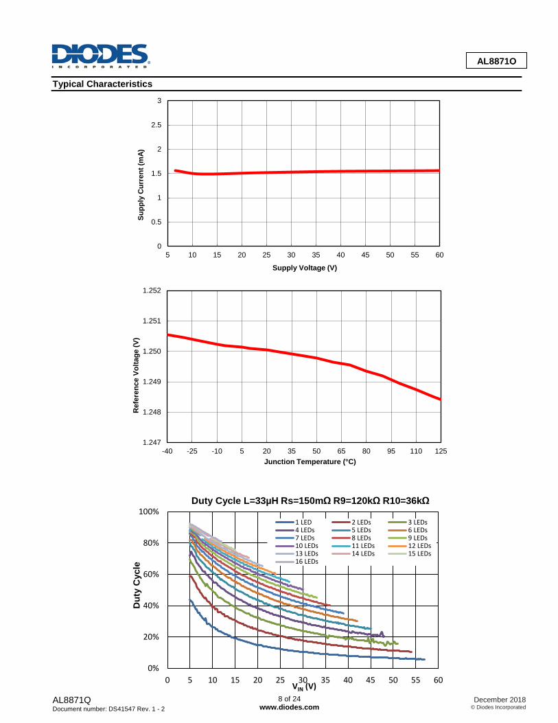
Typical Characteristics
0
0.5
1
1.5
2
2.5
3
5 10 15 20 25 30 35 40 45 50 55 60
Supp
ly C
urre
nt (m
A)
Supply Voltage (V)
1.247
1.248
1.249
1.250
1.251
1.252
-40 -25 -10 5 20 35 50 65 80 95 110 125
Ref
eren
ce V
olta
ge (V
)
Junction Temperature (°C)
0%
20%
40%
60%
80%
100%
0 5 10 15 20 25 30 35 40 45 50 55 60
Dut
y C
ycle
VIN (V)
Duty Cycle L=33µH Rs=150mΩ R9=120kΩ R10=36kΩ
1 LED 2 LEDs 3 LEDs4 LEDs 5 LEDs 6 LEDs7 LEDs 8 LEDs 9 LEDs10 LEDs 11 LEDs 12 LEDs13 LEDs 14 LEDs 15 LEDs16 LEDs
AL8871Q Document number: DS41547 Rev. 1 - 2
8 of 24 www.diodes.com
December 2018 © Diodes Incorporated
AL8871Q
Typical Characteristics—Analog/PWM Dimming
Typical Characteristics—Thermal Dimming
Switching Frequency
0
200
400
600
800
1000
1200
1400
0
50
100
150
200
250
300
350
0 0.25 0.5 0.75 1 1.25
Switc
hing
Fre
quen
cy (k
Hz)
LED
Cur
rent
(mA)
ADJ Voltage (V)
TA = 25°C VAUX = VIN = 24V 8 LEDs, GI = 0.23 L = 33µH, RS = 300mΩ
LED Current
0
250
500
750
1000
1250
1500
0% 20% 40% 60% 80% 100%
LED
Cur
rent
(mA)
PWM Duty Cycle
TA = 25°C fPWM = 100Hz VIN = VAUX = 24V L = 33µH, RS = 150mΩ
0%
20%
40%
60%
80%
100%
0 250 500 750 1000 1250
LED
Cur
rent
Dim
min
g Fa
ctor
TADJ Pin Voltage [mV]
AL8871Q Document number: DS41547 Rev. 1 - 2
9 of 24 www.diodes.com
December 2018 © Diodes Incorporated
AL8871Q
Typical Characteristics (RS = 150mΩ, ILED = 350mA, GIRATIO = 0.23)
0.15
0.20
0.25
0.30
0.35
0.40
0.45
5 6 7 8 9 10 11 12 13 14 15 16 17 18
LED
Cur
rent
(A)
VIN (V)
4 LEDs6 LEDs8 LEDs10 LEDs12 LEDs14 LEDs16 LEDs
TA = 25°C, VAUX = VIN L = 33µH, RS = 150mΩ, R9 = 120kΩ, R10 = 36kΩ, CIN = 100µF
0
100
200
300
400
500
600
700
5 8 11 14 17 20
Switc
hing
Fre
quen
cy (k
Hz)
Vin (V)
1 LED 2/3 LEDs
4 LEDs
5 LEDs 6 LEDs 7 LEDs 8 LEDs 9 LEDs
TA = 25°C, VAUX = VIN L = 33µH, RS = 150mΩ, R9 = 120kΩ, R10 = 36kΩ, CIN = 100µF
50%
55%
60%
65%
70%
75%
80%
85%
90%
5 8 11 14 17 20
Effic
ienc
y
Vin (V)
1 LED
4 LEDs
5 LEDs 6 LEDs
7 LEDs
8 LEDs
9 LEDs
TA = 25°C, VAUX = VIN L = 33µH, RS = 150mΩ, R9 = 120kΩ, R10 = 36kΩ, CIN = 100µF
3 LEDs
2 LEDs
AL8871Q Document number: DS41547 Rev. 1 - 2
10 of 24 www.diodes.com
December 2018 © Diodes Incorporated
AL8871Q
Typical Characteristics (RS = 150mΩ, ILED = 350mA, GIRATIO = 0.23)
L = 33µH
L = 68µH
L = 100µH
0.25
0.27
0.29
0.31
0.33
0.35
0.37
0.39
0.41
0.43
0.45
5 6 7 8 9 10 11 12 13 14 15 16 17 18
LED
Cur
rent
(A)
VIN (V)
TA = 25°C, VAUX = VIN, 8 LEDs, RS = 150mΩ, R9 = 120kΩ, R10 = 36kΩ, CIN = 100µF
0
50
100
150
200
250
300
350
400
450
500
5 6 7 8 9 10 11 12 13 14 15 16 17 18
Sw
itchi
ng F
requ
ency
(kHz
)
VIN (V)
8 LEDsL = 68µH
TA = 25°C, VAUX = VIN 8 LEDs, RS = 150mΩ, R9 = 120kΩ, R10 = 36kΩ, CIN = 100µF
L = 33µH
L = 100µH
40%
50%
60%
70%
80%
90%
100%
5 6 7 8 9 10 11 12 13 14 15 16 17 18
Effic
ienc
y
VIN (V)
TA = 25°C, VAUX = VIN 8 LEDs, RS = 150mΩ, R9 = 120kΩ, R10 = 36kΩ, CIN = 100µF
L = 68µH
L = 100µH
AL8871Q Document number: DS41547 Rev. 1 - 2
11 of 24 www.diodes.com
December 2018 © Diodes Incorporated
AL8871Q
Typical Characteristics (8 LEDs, L=33uH, GIRATIO = 0.23)
ILED = 150mA
0.10
0.15
0.20
0.25
0.30
0.35
0.40
0.45
0.50
0.55
0.60
5 6 7 8 9 10 11 12 13 14 15 16 17 18 19 20
LED
Cur
rent
(A)
VIN (V)
8 LEDsTA = 25°C, VAUX = VIN 8 LEDs, L = 33µH, R9 = 120kΩ, R10 = 36kΩ, CIN = 100µF
ILED = 500mA
ILED = 350mA
ILED = 350mA
ILED = 500mA
ILED = 150mA
0
100
200
300
400
500
600
700
800
5 6 7 8 9 10 11 12 13 14 15 16 17 18
Sw
itchi
ng F
requ
ency
(kH
z)
VIN (V)
TA = 25°C, VAUX = VIN 8 LEDs, L = 33µH R9 = 120kΩ, R10 = 36kΩ CIN = 100µF
ILED = 350mA
ILED = 500mA
ILED = 150mA
40%
50%
60%
70%
80%
90%
100%
5 6 7 8 9 10 11 12 13 14 15 16 17 18
Effic
ienc
y
VIN (V)
TA = 25°C, VAUX = VIN 8 LEDs, L = 33µH, R9 = 120kΩ, R10 = 36kΩ, CIN = 100µF
AL8871Q Document number: DS41547 Rev. 1 - 2
12 of 24 www.diodes.com
December 2018 © Diodes Incorporated
AL8871Q
Typical Characteristics—Bootstrap Performance
0.25
0.27
0.29
0.31
0.33
0.35
0.37
0.39
0.41
0.43
0.45
5 6 7 8 9 10 11 12 13 14 15 16 17 18
ILED
(A)
VIN (V)
Without bootstrap
With bootstrap
TA = 25°C, L = 33µH RS = 150mΩ, R9 = 120kΩ R10 = 36kΩ, VAUX = VIN Output=8LEDs
0
100
200
300
400
500
600
700
800
5 6 7 8 9 10 11 12 13 14 15 16 17 18
Switc
hing
Fre
quen
cy (k
Hz)
VIN (V)
Without bootstrap
With bootstrap
TA = 25°C, L = 33µH RS = 150mΩ, R9 = 120kΩ R10 = 36kΩ, VAUX = VIN Output=8LEDs
0%
10%
20%
30%
40%
50%
60%
70%
80%
90%
100%
5 6 7 8 9 10 11 12 13 14 15 16 17 18
Effic
ienc
y(%
)
VIN (V)
Without bootstrap
With bootstrap
TA = 25°C, L = 33µH RS = 150mΩ, R9 = 120kΩ R10 = 36kΩ, VAUX = VIN Output=8LEDs
AL8871Q Document number: DS41547 Rev. 1 - 2
13 of 24 www.diodes.com
December 2018 © Diodes Incorporated
AL8871Q
Application Information
The AL8871Q is a high-accuracy, hysteretic-inductive buck/boost/buck-boost controller designed to be used with an external NMOS switch for current-driving single or multiple series-connected LEDs. The device can be configured to operate in buck, boost, or buck-boost modes by suitable configuration of the external components as shown in the schematics. Device Description Resistor Rs connected between the two inputs of a current monitor within the control loop block senses the coil current. An output from the control-loop drives the input of a comparator, which drives the gate of the external NMOS switch transistor Q1 via the internal gate driver. When the switch is on, the drain voltage of Q1 is near zero. Current flows from VIN, via Rs, coil, and switch to ground. This current ramps up until an upper threshold value is reached (see Figure 3). At this point DRV goes low, the switch is turned off, and the drain voltage increases to the load voltage VLEDS plus the forward voltage of D1 plus VIN.
Gate Voltage
Q1 DrainVoltage
InductorCurrent
Sense Voltage
VIN-VISM
LED Current
0V
0V
+11~15V typ.
VLEDS+VF+VIN
Ipk
0A
0A
Mean=225mV*GI_ADJ/(1-D)
tOFF tON
Figure 3. Operating Waveforms
Current flows via Rs, coil, D1, and LED back to VIN. When the coil current ramps down to a lower threshold value, DRV goes high, the switch is turned on again, and the cycle of events repeats, which results in continuous oscillation. The feedback loop adjusts the NMOS switch duty cycle to stabilize the LED current in response to changes in external conditions, including input voltage and load voltage. Loop compensation is achieved by a single external capacitor C2 connected between COMP and SGND. Note that in reality, a load capacitor COUT is used, so the LED current waveform shown is smoothed. The average current in the sense resistor and coil, IRS, is equal to the average of the maximum and minimum threshold currents, and the ripple current (hysteresis) is equal to the difference between the thresholds. The average current in the LED, ILED, is always less than IRS. The feedback control loop adjusts the switch duty cycle, D, to achieve a set point at the sense resistor. This controls IRS. During the interval tOFF, the coil current flows through D1 and the LED load. During tON, the coil current flows through Q1—not the LEDs. Therefore, the set point is modified by D using a gating function to control ILED indirectly. In order to compensate internally for the effect of the gating function, a control factor GI_CTRL is used. GI_CTRL is set by a pair of external resistors RGI1 (R10) and RGI2
(R9) (see Figure 4). This allows the sense voltage to be adjusted to an optimum level for power efficiency without significant error in the LED controlled current.
GI_CTRL = RGI1RGI1 +RGI2
Equation 1
AL8871Q Document number: DS41547 Rev. 1 - 2
14 of 24 www.diodes.com
December 2018 © Diodes Incorporated
AL8871Q
Application Information (continued)
The control loop sets the duty cycle, so the sense resistor current is:
IRS= 0.225RS
GI_CTRL1-D
VCTRL
VREF Equation 2
IRS equals the coil current. The coil is only connected to the switch and the Schottky diode. The Schottky diode passes the LED current; therefore, the average LED current is the coil current multiplied by the Schottky diode duty cycle, 1-D.
ILED = IRS 1-D = 0.225RS
GI_CTRL VCTRLVREF
Equation 3
This shows that the LED current depends on the CTRL pin voltage, the reference voltage, and three resistor values (RS, RGI1, and RGI2). It is independent of the input and output voltages. If the CTRL pin is connected to the REF pin, it simplifies to:
ILED = 0.225RS
GI_CTRL Equation 4
Now ILED is dependent only on the three resistor values. Considering power dissipation and accuracy, it is useful to know how the mean sense voltage varies with input voltage and other parameters.
VRS= IRS RS = 0.225 GI_CTRL
1-D
VCTRLVREF
Equation 5
This shows that the sense voltage varies with duty cycle. Application Circuit Design External component selection is driven by the characteristics of the load and the input supply because this will determine the kind of topology is used for the system. Component selection begins with the current setting procedure, the inductor/frequency setting, and the MOSFET selection. Finally after selecting the freewheeling diode and the output capacitor (if required), the application section covers the PWM dimming and thermal feedback. The full procedure is greatly accelerated by the web calculator spreadsheet, which includes fully automated component selection and is available on the Diodes website; however, the full calculation is also given here. Please note the following particular feature of the web calculator. The GI ratio can be set for automatic calculation, or it can be fixed at a chosen value. When optimizing a design, it is best first to optimize for the chosen voltage range of most interest using the automatic setting. In order to subsequently evaluate performance of the circuit over a wider input voltage range, fix the GI ratio in the calculator input field, and set the desired input voltage range. Some components depend upon the switching frequency and the duty cycle. The switching frequency is regulated by the AL8871Q to a large extent depending upon conditions. This is discussed later in this document when dealing with coil selection. Duty Cycle Calculation The duty cycle is a function of the input and output voltages. Approximately, the MOSFET switching duty cycle is:
D≈ VOUTVOUT+VIN
Equation 6
Because D must always be a positive number less than 1, these equations show that VOUT > or = or < VIN. This allows topology selection for the required voltage range. The more exact equation used in the web calculator is:
D ≈ VOUT+VF+(IIN+IOUT)(RS+RCOIL)
VOUT+VIN+VF−VDSON Equation 7
Where: VF = Schottky diode forward voltage, estimated for the expected coil current, ICOIL VDSON = MOSFET drain source voltage in the ON condition (dependent on RDSON and drain current = ICOIL) RCOIL = DC winding resistance of L1
AL8871Q Document number: DS41547 Rev. 1 - 2
15 of 24 www.diodes.com
December 2018 © Diodes Incorporated
AL8871Q
Application Information (continued)
The additional terms are relatively small, so the exact equations only make a significant difference at lower operating voltages at the input and output, for example, low input voltage or a small number of LEDs connected in series. The estimates of VF and VDSON depend on the coil current. The mean coil current, ICOIL is calculated as follows:
ICOIL = IIN + ILED Equation 8 ILED is the target LED current and is already known. IIN is calculated with some accuracy later but can be estimated now from the electrical power efficiency. If the expected efficiency is roughly 90%, the output power POUT is 90% of the input power, PIN, and the coil current is estimated as follows:
POUT ≈ 0.9 PIN or ILED × N × VLED ≈ 0.9 IIN × VIN Where N is the number of LEDs connected in series, and VLED is the forward voltage drop of a single LED at ILED. So,
IIN≈ILED×𝑁×VLED
0.9VIN Equation 9
Equation 9 can now be used to find ICOIL in Equation 8, which can then be used to estimate the small terms in Equation 7. This completes the calculation of duty cycle. An initial estimate of duty cycle is required before choosing a coil. In Equation 7, the following approximations are recommended:
VF = 0.5V IIN × (RS + RCOIL) = 0.5V IOUT × (RS + RCOIL) = 0.5V VDSON = 0.1V (IIN + IOUT)(RS + RCOIL) = 1.1V
Then Equation 7 becomes:
D≈ VOUT+1.6VOUT+VIN+0.4
Equation 7a Setting the LED Current The LED current requirement determines the choice of the sense resistor Rs. This also depends on the voltage on the CTRL pin and the voltage on the GI pin according to the topology required. The CTRL pin can be connected directly to the internal 1.25V reference (VREF) to define the nominal 100% LED current. The CTRL pin can also be driven with an external DC voltage between 125mV and 1.25V to adjust the LED current proportionally between 10% and 100% of the nominal value. The divider ratio GI_CTRL is set less than 0.65V typically for optimized operation. This 0.65V threshold varies in proportion to VCTRL. CTRL and GI are high-impedance inputs within their normal operating voltage ranges. An internal 1.3V clamp protects the device against excessive input voltage and limits the maximum output current to approximately 4% above the maximum current set by VREF if the maximum input voltage is exceeded.
AL8871Q Document number: DS41547 Rev. 1 - 2
16 of 24 www.diodes.com
December 2018 © Diodes Incorporated
AL8871Q
Application Information (continued)
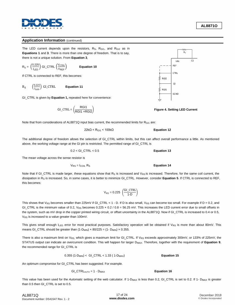
The LED current depends upon the resistors, RS, RGI1, and RGI2 as in Equations 1 and 3. There is more than one degree of freedom. That is to say, there is not a unique solution. From Equation 3,
RS = 0.225ILED
GI_CTRL VCTRLVREF
Equation 10
If CTRL is connected to REF, this becomes:
RS = 0.225ILED
GI_CTRL Equation 11
GI_CTRL is given by Equation 1, repeated here for convenience:
GI_CTRL = RGI1
RGI1 +RGI2
Figure 4. Setting LED Current
Note that from considerations of AL8871Q input bias current, the recommended limits for RGI1 are:
22kΩ < RGI1 < 100kΩ Equation 12 The additional degree of freedom allows the selection of GI_CTRL within limits, but this can affect overall performance a little. As mentioned above, the working voltage range at the GI pin is restricted. The permitted range of GI_CTRL is
0.2 < GI_CTRL < 0.5 Equation 13 The mean voltage across the sense resistor is
VRS = ICOIL RS Equation 14
Note that if GI_CTRL is made larger, these equations show that RS is increased and VRS is increased. Therefore, for the same coil current, the dissipation in RS is increased. So, in some cases, it is better to minimize GI_CTRL. However, consider Equation 5. If CTRL is connected to REF, this becomes:
VRS = 0.225 GI_CTRL
1-D
This shows that VRS becomes smaller than 225mV if GI_CTRL < 1 - D. If D is also small, VRS can become too small. For example if D = 0.2, and GI_CTRL is the minimum value of 0.2, VRS becomes 0.225 × 0.2 / 0.8 = 56.25 mV. This increases the LED current error due to small offsets in the system, such as mV drop in the copper printed wiring circuit, or offset uncertainty in the AL8871Q. Now if GI_CTRL is increased to 0.4 or 0.5, VRS is increased to a value greater than 100mV. This gives small enough ILED error for most practical purposes. Satisfactory operation will be obtained if VRS is more than about 80mV. This means GI_CTRL should be greater than (1-DMIN) × 80/225 = (1- DMIN) × 0.355. There is also a maximum limit on VRS, which gives a maximum limit for GI_CTRL. If VRS exceeds approximately 300mV, or 133% of 225mV, the STATUS output can indicate an overcurrent condition. This will happen for larger DMAX. Therefore, together with the requirement of Equation 9, the recommended range for GI_CTRL is
0.355 (1-DMIN) < GI_CTRL < 1.33 ( 1-DMAX) Equation 15 An optimum compromise for GI_CTRL has been suggested. For example.
GI_CTRLAUTO = 1 - DMAX Equation 16 This value has been used for the Automatic setting of the web calculator. If 1-DMAX is less than 0.2, GI_CTRL is set to 0.2. If 1- DMAX is greater than 0.5 then GI_CTRL is set to 0.5. AL8871Q Document number: DS41547 Rev. 1 - 2
17 of 24 www.diodes.com
December 2018 © Diodes Incorporated
AL8871Q
Application Information (continued)
Once GI_CTRL is selected, a value of RGI1 can be selected from Equation 8. Then RGI2 is calculated as follows, rearranging Equation 1:
RGI2 = RGI1 1-GI_CTRLGI_CTRL
Equation 17
For example driving 12 LEDS at a current of 350mA from a 12V supply, each LED has a forward voltage of 3.2V at 350mA, so Vout = 3.2 × 12 = 38.4V. The duty cycle is approximately
VOUT-VINVOUT
= 38.4-1238.4
= 0.6875
From Equation 12, we set GI_CTRL to 1 – D = 0.3125. IF RGI1 = 33kΩ, then from Equation 3, RGI2 = 33000 × (1 -0.3125) / 0.3125 = 72.6kΩ. Select the preferred value RGI2 = 75kΩ. Now GI_CTRL is adjusted to the new value using Equation 1.
GI_CTRL = RGI1
RGI1 +RGI2 =
33k33k +75k
=0.305
Now calculate Rs from Equation 6. Assume CTRL is connected to REF.
RS = 0.225ILED
GI_CTRLVCTRL
VREF =
0.2250.35
* 0.305 = 0.196 Ω
A preferred value of RS = 0.2Ω gives the desired LED current with an error of 2% due to the preferred value selection. Table 1 shows typical resistor values used to determine the GI_CTRL ratio with E24 series resistors.
Table 1 GI ratio RGI1 RG2
0.2 30kΩ 120kΩ 0.25 33kΩ 100kΩ 0.3 39kΩ 91kΩ 0.35 30kΩ 56kΩ 0.4 100kΩ 150kΩ 0.45 51kΩ 62kΩ 0.5 30kΩ 30kΩ
This completes the LED current setting.
AL8871Q Document number: DS41547 Rev. 1 - 2
18 of 24 www.diodes.com
December 2018 © Diodes Incorporated
AL8871Q
Application Information (continued)
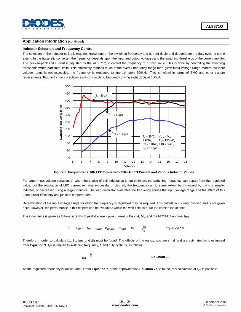
Inductor Selection and Frequency Control The selection of the inductor coil, L1, requires knowledge of the switching frequency and current ripple and depends on the duty cycle to some extent. In the hysteretic converter, the frequency depends upon the input and output voltages and the switching thresholds of the current monitor. The peak-to-peak coil current is adjusted by the AL8871Q to control the frequency to a fixed value. This is done by controlling the switching thresholds within particular limits. This effectively reduces much of the overall frequency range for a given input voltage range. Where the input voltage range is not excessive, the frequency is regulated to approximately 390kHz. This is helpful in terms of EMC and other system requirements. Figure 5 shows practical results of switching frequency driving eight LEDs at 350mA.
Figure 5. Frequency vs. VIN LED Driver with 350mA LED Current and Various Inductor Values
For larger input voltage variation, or when the choice of coil inductance is not optimum, the switching frequency can depart from the regulated value, but the regulation of LED current remains successful. If desired, the frequency can to some extent be increased by using a smaller inductor, or decreased using a larger inductor. The web calculator evaluates the frequency across the input voltage range and the effect of this upon power efficiency and junction temperatures. Determination of the input voltage range for which the frequency is regulated may be required. This calculation is very involved and is not given here. However, the performance in this respect can be evaluated within the web calculator for the chosen inductance. The inductance is given as follows in terms of peak-to-peak ripple current in the coil, ΔIL, and the MOSFET on time, tON.
L1 = 𝑉𝐼𝑁 − (𝐼𝐼𝑁 + 𝐼𝑂𝑈𝑇)(𝑅𝐷𝑆𝑂𝑁 + 𝑅𝐶𝑂𝐼𝐿 + 𝑅𝑆) × 𝑡𝑂𝑁∆𝐼𝐿
Equation 18
Therefore In order to calculate L1, IIN, tON, and ΔIL must be found. The effects of the resistances are small and are estimated.IIN is estimated from Equation 9. tON is related to switching frequency, f, and duty cycle, D, as follows:
tON= Df Equation 19
As the regulated frequency is known, and D from Equation 7, or the approximation Equation 7a, is found, this calculation of tON is possible.
0
50
100
150
200
250
300
350
400
450
500
5 6 7 8 9 10 11 12 13 14 15 16 17 18
Sw
itchi
ng F
requ
ency
(kHz
)
VIN (V)
8 LEDsL = 68µH
TA = 25°C, VAUX = VIN 8 LEDs, RS = 150mΩ, R9 = 120kΩ, R10 = 36kΩ, CIN = 100µF
L = 33µH
L = 68µH
L = 100µH
AL8871Q Document number: DS41547 Rev. 1 - 2
19 of 24 www.diodes.com
December 2018 © Diodes Incorporated
AL8871Q
Application Information (continued)
The AL8871Q sets the ripple current, ΔIL, to between nominally 10% and 30% of the mean coil current, ICOIL, which is found from Equation 8. The device adjusts the ripple current within this range in order to regulate the switching frequency. A ΔIL value of 20% of ICOIL must be used to find an inductance, which is optimized for the input voltage range. The range of ripple current control is also modulated by other circuit parameters as follows.
∆𝐼𝐿𝑀𝐴𝑋 = 0.06 + 0.24(𝑉𝐴𝐷𝐽𝑉𝑅𝐸𝐹
) × 1−𝐷𝐺𝐼_𝐴𝐷𝐽
× 𝐼𝐶𝑂𝐼𝐿
∆𝐼𝐿𝑀𝐼𝑁 = 0.02 + 0.08(𝑉𝐴𝐷𝐽𝑉𝑅𝐸𝐹
) × 1−𝐷𝐺𝐼_𝐴𝐷𝐽
× 𝐼𝐶𝑂𝐼𝐿 Equation 20
∆𝐼𝐿𝑀𝐼𝐷 = 0.04 + 0.16(𝑉𝐴𝐷𝐽𝑉𝑅𝐸𝐹
) × 1−𝐷𝐺𝐼_𝐴𝐷𝐽
× 𝐼𝐶𝑂𝐼𝐿
If ADJ is connected to REF, this simplifies to
∆𝐼𝐿𝑀𝐴𝑋 = 0.3 ×1 − 𝐷𝐺𝐼_𝐴𝐷𝐽 × 𝐼𝐶𝑂𝐼𝐿
∆𝐼𝐿𝑀𝐼𝑁 = 0.1 × 1−𝐷𝐺𝐼_𝐴𝐷𝐽
× 𝐼𝐶𝑂𝐼𝐿 Equation 20a
∆𝐼𝐿𝑀𝐼𝐷 = 0.2 ×1 −𝐷𝐺𝐼_𝐴𝐷𝐽 × 𝐼𝐶𝑂𝐼𝐿
Where ΔILMID is the value of we must use in Equation 18. The inductance value is now established. The chosen coil must saturate at a current greater than the peak sensed current. This saturation current is the DC current for which the inductance has decreased by 10% compared to the low current value. Assuming ±10% ripple current, the peak current can be found from Equation 8, which is adjusted for ripple current:
ICOILPEAK = 1.1 IINMAX + ILED Equation 21
Where IINMAX is the value of IIN at minimum VIN. The mean current rating is also a factor, but normally the saturation current is the limiting factor. LED Current Dimming The AL8871Q has three dimming methods for reducing the average LED current:
1. DC dimming using the CTRL pin 2. PWM dimming using the PWM pin 3. DC dimming for thermal protection using the NTC pin
DC or Analog Dimming The AL8871Q has a clamp on the CTRL pin to prevent overdriving of the LED current, which results in applying the maximum voltage to internal circuitry as the reference voltage. This provides a 10:1 dynamic range of DC LED current adjustment. The equation for DC dimming of the LED current is approximately:
ILED_DIM=ILED_NOM VCTRL
VREF
Where:
• ILED_DIM is the dimmed LED current • ILED_NOM is the LED current with VCTRL = 1.25V
One consequence of DC dimming is as the CTRL pin voltage reduces, the sense voltage also be reduces, which has an impact on accuracy and switching frequency especially at lower CTRL pin voltages.
AL8871Q Document number: DS41547 Rev. 1 - 2
20 of 24 www.diodes.com
December 2018 © Diodes Incorporated
AL8871Q
Application Information (continued)
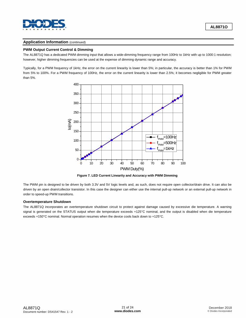
PWM Output Current Control & Dimming The AL8871Q has a dedicated PWM dimming input that allows a wide-dimming frequency range from 100Hz to 1kHz with up to 1000:1 resolution; however, higher dimming frequencies can be used at the expense of dimming dynamic range and accuracy. Typically, for a PWM frequency of 1kHz, the error on the current linearity is lower than 5%; in particular, the accuracy is better than 1% for PWM from 5% to 100%. For a PWM frequency of 100Hz, the error on the current linearity is lower than 2.5%; it becomes negligible for PWM greater than 5%.
0 10 20 30 40 50 60 70 80 90 1000
50
100
150
200
250
300
350
400
Io(m
A)
PWM Duty(%)
fPWM=100Hz fPWM=500Hz fPWM=1kHz
Figure 7. LED Current Linearity and Accuracy with PWM Dimming
The PWM pin is designed to be driven by both 3.3V and 5V logic levels and, as such, does not require open collector/drain drive. It can also be driven by an open drain/collector transistor. In this case the designer can either use the internal pull-up network or an external pull-up network in order to speed-up PWM transitions.
Overtemperature Shutdown The AL8871Q incorporates an overtemperature shutdown circuit to protect against damage caused by excessive die temperature. A warning signal is generated on the STATUS output when die temperature exceeds +125°C nominal, and the output is disabled when die temperature exceeds +150°C nominal. Normal operation resumes when the device cools back down to +125°C.
AL8871Q Document number: DS41547 Rev. 1 - 2
21 of 24 www.diodes.com
December 2018 © Diodes Incorporated
AL8871Q
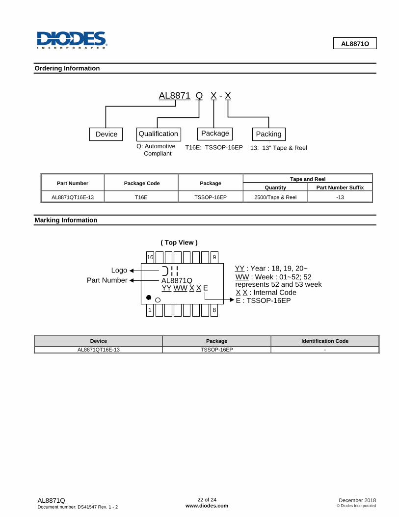
Ordering Information
AL8871 Q– X - X
Package Packing
T16E: TSSOP-16EP 13: 13" Tape & Reel
Device Qualification
Q: Automotive Compliant
Part Number Package Code Package Tape and Reel
Quantity Part Number Suffix
AL8871QT16E-13 T16E TSSOP-16EP 2500/Tape & Reel -13
Marking Information
( Top View )
1
AL8871QYY WW X X E
LogoPart Number
8
WW : Week : 01~52; 52YY : Year : 18, 19, 20~
X X : Internal Coderepresents 52 and 53 week
16 9
E : TSSOP-16EP
Device Package Identification Code AL8871QT16E-13 TSSOP-16EP -
AL8871Q Document number: DS41547 Rev. 1 - 2
22 of 24 www.diodes.com
December 2018 © Diodes Incorporated
AL8871Q
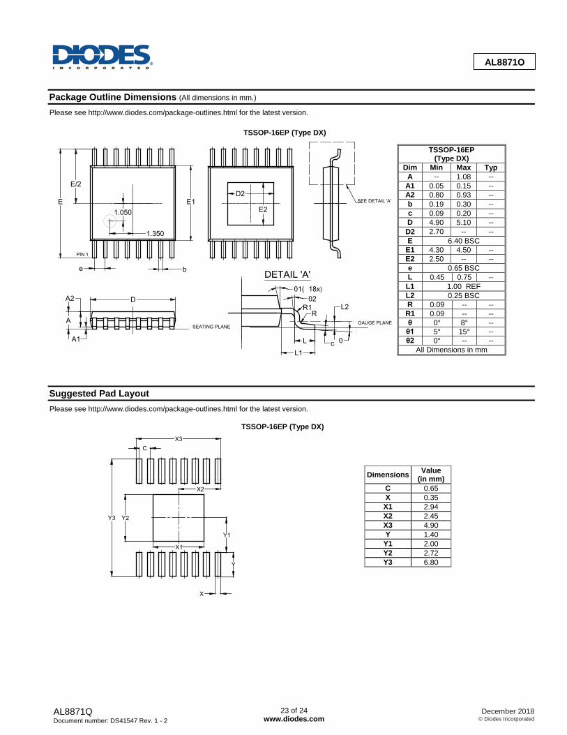
Package Outline Dimensions (All dimensions in mm.) Please see http://www.diodes.com/package-outlines.html for the latest version.
TSSOP-16EP (Type DX)
TSSOP-16EP (Type DX)
Dim Min Max Typ A -- 1.08 -- A1 0.05 0.15 -- A2 0.80 0.93 -- b 0.19 0.30 -- c 0.09 0.20 -- D 4.90 5.10 -- D2 2.70 -- -- E 6.40 BSC
E1 4.30 4.50 -- E2 2.50 -- -- e 0.65 BSC L 0.45 0.75 --
L1 1.00 REF L2 0.25 BSC R 0.09 -- -- R1 0.09 -- -- θ 0° 8° -- θ1 5° 15° -- θ2 0° -- --
All Dimensions in mm
Suggested Pad Layout Please see http://www.diodes.com/package-outlines.html for the latest version.
TSSOP-16EP (Type DX)
Dimensions Value (in mm)
C 0.65 X 0.35
X1 2.94 X2 2.45 X3 4.90 Y 1.40
Y1 2.00 Y2 2.72 Y3 6.80
SEATING PLANE
A2
A
D
A1
DETAIL 'A'
GAUGE PLANE
R1R
LL1
L2
0
01( 18x)02
SEE DETAIL 'A'
E2
D2
c
PIN 1
e b
E
E/2
E1
1.350
1.050
C
Y2
X1
Y
X
X2
Y1
Y3
X3
AL8871Q Document number: DS41547 Rev. 1 - 2
23 of 24 www.diodes.com
December 2018 © Diodes Incorporated
AL8871Q
IMPORTANT NOTICE DIODES INCORPORATED MAKES NO WARRANTY OF ANY KIND, EXPRESS OR IMPLIED, WITH REGARDS TO THIS DOCUMENT, INCLUDING, BUT NOT LIMITED TO, THE IMPLIED WARRANTIES OF MERCHANTABILITY AND FITNESS FOR A PARTICULAR PURPOSE (AND THEIR EQUIVALENTS UNDER THE LAWS OF ANY JURISDICTION). Diodes Incorporated and its subsidiaries reserve the right to make modifications, enhancements, improvements, corrections or other changes without further notice to this document and any product described herein. Diodes Incorporated does not assume any liability arising out of the application or use of this document or any product described herein; neither does Diodes Incorporated convey any license under its patent or trademark rights, nor the rights of others. Any Customer or user of this document or products described herein in such applications shall assume all risks of such use and will agree to hold Diodes Incorporated and all the companies whose products are represented on Diodes Incorporated website, harmless against all damages. Diodes Incorporated does not warrant or accept any liability whatsoever in respect of any products purchased through unauthorized sales channel. Should Customers purchase or use Diodes Incorporated products for any unintended or unauthorized application, Customers shall indemnify and hold Diodes Incorporated and its representatives harmless against all claims, damages, expenses, and attorney fees arising out of, directly or indirectly, any claim of personal injury or death associated with such unintended or unauthorized application. Products described herein may be covered by one or more United States, international or foreign patents pending. Product names and markings noted herein may also be covered by one or more United States, international or foreign trademarks. This document is written in English but may be translated into multiple languages for reference. Only the English version of this document is the final and determinative format released by Diodes Incorporated.
LIFE SUPPORT Diodes Incorporated products are specifically not authorized for use as critical components in life support devices or systems without the express written approval of the Chief Executive Officer of Diodes Incorporated. As used herein: A. Life support devices or systems are devices or systems which: 1. are intended to implant into the body, or
2. support or sustain life and whose failure to perform when properly used in accordance with instructions for use provided in the labeling can be reasonably expected to result in significant injury to the user.
B. A critical component is any component in a life support device or system whose failure to perform can be reasonably expected to cause the failure of the life support device or to affect its safety or effectiveness. Customers represent that they have all necessary expertise in the safety and regulatory ramifications of their life support devices or systems, and acknowledge and agree that they are solely responsible for all legal, regulatory and safety-related requirements concerning their products and any use of Diodes Incorporated products in such safety-critical, life support devices or systems, notwithstanding any devices- or systems-related information or support that may be provided by Diodes Incorporated. Further, Customers must fully indemnify Diodes Incorporated and its representatives against any damages arising out of the use of Diodes Incorporated products in such safety-critical, life support devices or systems. Copyright © 2018, Diodes Incorporated www.diodes.com
AL8871Q Document number: DS41547 Rev. 1 - 2
24 of 24 www.diodes.com
December 2018 © Diodes Incorporated