Embed Size (px)
Citation preview

○Product structure:Silicon monolithic integrated circuit ○This product has no designed protection against radioactive rays
1/23 © 2014 ROHM Co., Ltd. All rights reserved. www.rohm.com
TSZ22111・14・001
TSZ02201-0Q3Q0NZ00320-1-2
16.Feb.2015 Rev.002
2.7V to 14V
Synchronous Buck-Boost Controller BD8303MUV General Description
BD8303MUV is ROHM’s high efficiency step-up/step-down switching regulator IC. It produces output of 3.3V / 5V from 1 cell of lithium battery, 4 batteries, or 2 cells of Li batteries with just one inductor. This IC uses an original step-up/step-down drive system and provides a higher efficient power supply than conventional SEPIC-system or H-bridge system switching regulators.
Features Highly-Efficient Step-Up/Step-Down DC/DC
Converter Implemented with Just One Inductor Supports High-Current Applications with External
N-Channel FET Incorporates a Soft-Start Function Incorporates a Timer-Latch System with Short
Circuit Protection Function
Applications General Portable Equipment DVC Single-Lens Reflex Cameras Portable DVDs Mobile PCs
Key Specifications Input Voltage Range: +2.7V to +14V Reference Volatage Accuracy : 1.25% Standby Current: 0μA(Typ) Operating Temperature Range: -25°C to +85°C
Package W(Typ) x D(Typ) x H(Max)
Typical Application Circuit
VCC=4.0~14V, VOUT=8.4V, IOUT=100mA ~ 1500mA
VQFN016V3030
3.00mm x 3.00mm x 1.00mm
VCC =
4.0V – 14V
Insert a filter as required.
1μF
RB521CS-30
RB521CS-30
0.1μF 4.7μH RSS065N03
47μF x 2
0.1μF
ON/OFF
27kΩ
7.5kΩ
200kΩ
100kΩ
3.9kΩ
4700pF
100pF
RSS065N03
RSS065N03
RSS065N03
47μF 0.1μF
RT SW1 VC
C
INV
FB
GND
VR
EG
BO
OT
1
HG
1
LG1
PGND
LG2
ST
B
BO
OT
2
HG
2
SW
2
(TDK SLF10165) VOUT (set at 8.4 V)
Datasheet
2/23
BD8303MUV
© 2014 ROHM Co., Ltd. All rights reserved. www.rohm.com
TSZ22111・15・001
TSZ02201-0Q3Q0NZ00320-1-2
16.Feb.2015 Rev.002
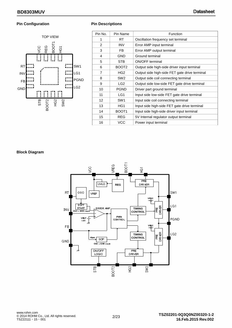
Pin Configuration Pin Descriptions
Block Diagram
Pin No. Pin Name Function
1 RT Oscillation frequency set terminal
2 INV Error AMP input terminal
3 FB Error AMP output terminal
4 GND Ground terminal
5 STB ON/OFF terminal
6 BOOT2 Output side high-side driver input terminal
7 HG2 Output side high-side FET gate drive terminal
8 SW2 Output side coil connecting terminal
9 LG2 Output side low-side FET gate drive terminal
10 PGND Driver part ground terminal
11 LG1 Input side low-side FET gate drive terminal
12 SW1 Input side coil connecting terminal
13 HG1 Input side high-side FET gate drive terminal
14 BOOT1 Input side high-side driver input terminal
15 REG 5V Internal regulator output terminal
16 VCC Power input terminal
TOP VIEW V
CC
RE
G
BO
OT
1
HG
1
ST
B
BO
OT
2
HG
2
SW
2
RT
INV
FB
GND
SW1
LG1
LG2
PGND
RE
G
REG
TIMING CONTROL
TIMING
CONTROL

3/23
BD8303MUV
© 2014 ROHM Co., Ltd. All rights reserved. www.rohm.com
TSZ22111・15・001
TSZ02201-0Q3Q0NZ00320-1-2
16.Feb.2015 Rev.002
Description of Blocks
1. VREF This block generates ERROR AMP reference voltage. The reference voltage is set to 1.0V.
2. VREG This is a voltage regulator block which outputs 5.0V and is used as power supply for IC internal circuit and BOOT pin supply. Follows power supply voltage when 5.0V or below while the output voltage drops at the same time. An external 1.0µF capacitor is recommended to prevent oscillation.
3. UVLO This block prevents the malfunction of the internal circuitry during start-up or when the supply drops below a certain voltage. When VREG is below 2.4V, the HG1, HG2, LG1 and LG2 pin is low, this block turns OFF all FET and DC/DC converter outputs and resets the timer latch of the internal SCP circuit and soft-start circuit
4. SCP This block is the Short Circuit Protection that uses a Timer Latch System. It has an internal counter that is in synch with OSC. When the INV pin is set to 1.0V or lower voltage, the internal counter will count about 8200 pulses after which the latch circuit will activate Turning OFF the DC/DC converter output (13.6msec when RRT = 51kΩ). Restarting the STB pin or the supply voltage will reset the latch circuit.
5. OSC The OSC block generates the internal frequency of the IC. The frequency can be varied depending on the value of the external resistance of the RT pin (Pin 1).When RRT = 51kΩ, the operation frequency is set to 600kHz.
6. ERROR AMP The ERROR AMP block detects output signals and PWM control signals and compares them with an internal reference voltage set at 1.0V.
7. PWM COMP The PWM COMP block is a Voltage-to-Pulse Width converter that controls the output voltage depending on the input voltage. This block controls the pulse width by comparing the internal SLOPE waveform with the ERROR AMP output voltage. The output signal of the PWM COMP block is then fed to the driver. Max Duty and Min Duty are set at the primary side and the secondary side of the inductor respectively, which are as follows:
Primary side (SW1) HG1 Max Duty : About 90%, HG1 Min Duty : 0 % Secondary side (SW2) LG2 Max Duty : About 90%, LG2 Min Duty : About 10%,
8. SOFT START This block prevents in-rush current during start-up by bringing the output voltage of the DCDC converter into a soft-start. The Soft-Start block is in synch with the internal OSC block. This block enables the output voltage of the DCDC converter to reach the set voltage after about 2400 pulses (4msec when RRT = 51kΩ).
9. N-Channel DRIVER This block consists of a CMOS inverter circuit that drives the built-in N-Channel FET. It provides dead time for preventing feed through during switching of HG1 = L to LG1 = H to HG2 = L to LG2 = H and LG1 = L to HG1 = H, LG2 = L to HG2 = H. The dead time is set at about 100nsec for each individual SWs
10. ON/OFF LOGIC This block enables and disables the IC depending on the voltage applied at STB pin (Pin 5). The IC Turns ON when STB voltage is 2.5 V or higher and it Turns OFF when STB is open or when 0V is applied. The STB pin has a pull-down resistor of approximately 400kΩ.

4/23
BD8303MUV
© 2014 ROHM Co., Ltd. All rights reserved. www.rohm.com
TSZ22111・15・001
TSZ02201-0Q3Q0NZ00320-1-2
16.Feb.2015 Rev.002
Absolute Maximum Ratings
Parameter Symbol Rating Unit
Maximum Applied Power Voltage
VCC 15 V
VREG 7 V
Between VBOOT1 , VBOOT2 and VSW1, VSW2
7 V
Between VBOOT1 , VBOOT2
and GND 20 V
VSW1 and VSW2 15 V
Power Dissipation Pd 0.62 (Note 1)
W
Operating Temperature Range Topr -25 to +85 °C
Storage Temperature Range Tstg -55 to +150 °C
Junction Temperature Tjmax +150 °C
(Note 1) When installed on a 70.0 mm x 70.0 mm x 1.6 mm glass epoxy board. The rating is reduced by 4.96 mW/°C at Ta = 25°C or more. Caution: Operating the IC over the absolute maximum ratings may damage the IC. The damage can either be a short circuit between pins or an open circuit between pins and the internal circuitry. Therefore, it is important to consider circuit protection measures, such as adding a fuse, in case the IC is operated over the absolute maximum ratings.
Recommended Operating Conditions
Parameter Symbol Standard Value
Unit Min Typ Max
Power Supply Voltage Range VCC 2.7 - 14 V
Output Voltage Range VOUT 1.8 - 12 V
Oscillation Frequency Range fOSC 0.2 0.6 1.0 MHz

5/23
BD8303MUV
© 2014 ROHM Co., Ltd. All rights reserved. www.rohm.com
TSZ22111・15・001
TSZ02201-0Q3Q0NZ00320-1-2
16.Feb.2015 Rev.002
Electrical Characteristics (Unless otherwise specified, Ta = 25°C, VCC = 7.4V)
Parameter Symbol Target Value
Unit Conditions Minimum Typical Maximum
UVLO
Detection Threshold Voltage VUV - 2.4 2.6 V VREG monitor
Hysteresis Range ΔVUVHY 50 100 200 mV
Oscillator
Oscillation Frequency fOSC 480 600 720 kHz RRT=51kΩ
Regulator
Output Voltage VREG 4.7 5.1 5.5 V
Error AMP
INV Threshold Voltage VINV 0.9875 1.00 1.0125 V
Input Bias Current IINV -50 0 +50 nA VCC=12.0V, VINV=6.0V
Soft-Start Time tSS 2.4 4.0 5.6 msec RRT=51kΩ
Output Source Current IEO 10 20 30 μA VINV=0.8V , VFB=1.5V
Output Sink Current IEI 0.6 1.3 3 mA VINV=1.2V , VFB=1.5V
PWM Comparator
SW1 Max Duty DMAX1 85 90 95 % HG1 ON
SW2 Max Duty DMAX2 85 90 95 % LG2 ON
SW2 Min Duty DMIN2 5 10 15 % LG2 OFF
Output
HG1, 2 High side ON-Resistance RONHP - 4 8 Ω
HG1, 2 Low side ON-Resistance RONHN - 4 8 Ω
LG1, 2 High side ON-Resistance RONLP - 4 8 Ω
LG1, 2 Low side ON-Resistance RONLN - 4 8 Ω
HG1-LG1 Dead Time tDEAD1 50 100 200 nsec
HG2-LG2 Dead Time tDEAD2 50 100 200 nsec
STB
STB pin Control Voltage
Operation VSTBH 2.5 - VCC V
No-Operation VSTBL -0.3 - +0.3 V
STB Pin Pull-Down Resistance RSTB 250 400 700 kΩ
Circuit Current
Standby Current VCC Pin ISTB - - 1 μA
VCC Circuit Current ICC1 - 650 1000 μA VINV=1.2V
BOOT1 and BOOT2 Circuit Current ICC2 - 120 240 μA VINV=1.2V

6/23
BD8303MUV
© 2014 ROHM Co., Ltd. All rights reserved. www.rohm.com
TSZ22111・15・001
TSZ02201-0Q3Q0NZ00320-1-2
16.Feb.2015 Rev.002
Typical Performance Curves (Unless otherwise specified, Ta = 25°C, VCC = 7.4V)
Figure 1. VREF Voltage vs VCC Voltage
VCC Voltage [V]
VR
EF
Vo
ltag
e [
V]
0.950
0.975
1.000
1.025
1.050
0 5 10 15
Figure 2. VREF Voltage vs Ambient Temperature
Ambient Temperature [°C]
VR
EF
Vo
ltag
e [
V]
0.950
0.975
1.000
1.025
1.050
-40 0 40 80 120
Figure 3. REG Voltage vs VCC Voltage
VCC Voltage [V]
RE
G V
olta
ge :
VR
EG
[V]
0.0
1.0
2.0
3.0
4.0
5.0
6.0
0 5 10 15
Figure 4. REG Voltage vs Ambient Temperature
Ambient Temperature [°C]
RE
G V
olta
ge :
VR
EG
[V]
4.700
4.800
4.900
5.000
5.100
5.200
5.300
-40 0 40 80 120

7/23
BD8303MUV
© 2014 ROHM Co., Ltd. All rights reserved. www.rohm.com
TSZ22111・15・001
TSZ02201-0Q3Q0NZ00320-1-2
16.Feb.2015 Rev.002
Typical Performance Curves - continued
Figure 5. Oscillation Frequency vs VCC Voltage
VCC Voltage [V]
Oscill
atio
n F
req
ue
ncy [kH
z]
400
500
600
700
800
0 5 10 15
Figure 6. Oscillation Frequency vs Ambient Temperature
Ambient Temperature [°C] O
scill
atio
n F
req
ue
ncy [kH
z]
500
520
540
560
580
600
620
640
660
680
700
-40 0 40 80 120
Figure 7. VCC Current vs VCC Voltage
VCC Voltage [V]
VC
C C
urr
en
t [μ
A]
0
100
200
300
400
500
600
700
800
900
0 5 10 15
Figure 8. VCC Current vs Ambient Temperature
Ambient Temperature [°C]
VC
C C
urr
en
t [μ
A]
500
550
600
650
700
750
800
-40 0 40 80 120

8/23
BD8303MUV
© 2014 ROHM Co., Ltd. All rights reserved. www.rohm.com
TSZ22111・15・001
TSZ02201-0Q3Q0NZ00320-1-2
16.Feb.2015 Rev.002
Typical Performance Curves - continued
Figure 9. BOOT Pin Current vs BOOT Pin Voltage
BO
OT
Pin
Cu
rre
nt
[μA
]
BOOT Pin Voltage [V]
0
20
40
60
80
100
120
140
0 1 2 3 4 5 6
Figure 10. OUT Voltage vs VCC Voltage (Line Regulation)
VCC Voltage [V]
OU
T V
oltag
e :
VO
UT [
V]
4.950
4.975
5.000
5.025
5.050
0 5 10 15
Load Current [mA]
OU
T V
oltag
e :
VO
UT [
V]
4.950
4.975
5.000
5.025
5.050
0 500 1000 1500
Figure 12. MAX Duty / MIN Duty vs Ambient Temperature
Ambient Temperature [℃]
Duty
[%
]
0
10
20
30
40
50
60
70
80
90
100
-40 0 40 80 120
SW1 Max Duty
SW2 Max Duty
SW2 Min Duty
Figure 11. OUT Voltage vs Load Current (Load Regulation)

9/23
BD8303MUV
© 2014 ROHM Co., Ltd. All rights reserved. www.rohm.com
TSZ22111・15・001
TSZ02201-0Q3Q0NZ00320-1-2
16.Feb.2015 Rev.002
Typical Performance Curves - continued
Figure 13. Efficiency vs Load Current (Example of Application Circuit [1]
(VOUT = 3.3V))
Load Current [mA]
Effic
iency [
%]
0
10
20
30
40
50
60
70
80
90
100
0 1000 2000 3000
VCC=3.0V
VCC=3.7V
VCC=5.0V
VCC=4.2V
Figure 14. Efficiency vs Load Current (Example of Application Circuit [2]
(VOUT = 5.0V))
Load Current [mA] E
ffic
iency [
%]
0
10
20
30
40
50
60
70
80
90
100
0 500 1000 1500
VCC=4.0V
VCC=14V
VCC=7.4V
Figure 15. Efficiency vs Load Current (Example of Application Circuit [3]
(VOUT = 8.4V)
Load Current [mA]
Effic
iency [
%]
0
10
20
30
40
50
60
70
80
90
100
0 500 1000 1500 2000
VCC=4.0V
VCC=10V
VCC=7.4V

10/23
BD8303MUV
© 2014 ROHM Co., Ltd. All rights reserved. www.rohm.com
TSZ22111・15・001
TSZ02201-0Q3Q0NZ00320-1-2
16.Feb.2015 Rev.002
Typical Waveforms
Figure 18. Load Variation Waveform Example of Application Circuit [2]
(VCC = 7.4V, VOUT = 5.0V, ILOAD = 200mA ↔1000mA :40 mA/µsec)
VOUT (100mV/div)
ILOAD(500mA/div)
500μsec/div
Figure 17. Oscillation Waveform (VCC = 5.0V, VOUT = 5.0V, ILOAD = 1000mA)
500nsec/div
Figure 16. Starting Waveform Example of Application Circuit [2]
(L=10µH, COUT = 47µH, fOSC = 750 kHz, unloaded)
VOUT (2.0V/div)
200μsec/div

11/23
BD8303MUV
© 2014 ROHM Co., Ltd. All rights reserved. www.rohm.com
TSZ22111・15・001
TSZ02201-0Q3Q0NZ00320-1-2
16.Feb.2015 Rev.002
Application Information
1. Package Heat Reduction Curve
2. Example of Application Circuit
(1) Application Circuit [1]: Input: 2.7V to 5.5V, Output: 3.3V / 100mA to 2000mA
Figure 19. Power Dissipation vs Ambient Temperature Heat Reduction Curve (IC alone)
when used at Ta = 25°C or more, it is reduced by 4.96 mW/°C.
Ambient Temperature [°C]
Pow
er
Dis
sip
ation [
mW
]
Figure 20. Example of Application Circuit [1]
VOUT (set at 3.3 V)
Insert a filter as required.
1μF
RB521CS-30
RB521CS-30
0.1μF 4.7μH
RTQ045N03
47μF
0.1μF
ON/OFF
43kΩ
7.5kΩ
100kΩ
51kΩ
6.2kΩ
10000pF
150pF
RTQ045N03
RTQ045N03
RTQ045N03
22μF 0.1μF
RT SW1 VC
C
INV
FB
GND
VR
EG
BO
OT
1
HG
1
LG1
PGND
LG2
ST
B
BO
OT
2
HG
2
SW
2
VCC =
2.7 V – 5.5 V
(TDK SLF10165)

12/23
BD8303MUV
© 2014 ROHM Co., Ltd. All rights reserved. www.rohm.com
TSZ22111・15・001
TSZ02201-0Q3Q0NZ00320-1-2
16.Feb.2015 Rev.002
(2) Application Circuit [2]: Input: 2.7V to 14 V, Output : 5.0V / 100 mA to 1500 mA
(3) Application Circuit [3]: Input : 4.0V to 14V, Output : 8.4V / 100mA to 1500mA
Figure 21. Example of Application Circuit [2]
Insert a filter as required.
VOUT (set at 5.0 V)
1μF
RB521CS-30
RB521CS-30
0.1μF 4.7μH
RTQ045N03
VCC =
2.7 V –14 V
47μF
0.1μF
ON/OFF
30kΩ
5.1kΩ 120kΩ
51kΩ
4.7kΩ
4700pF
120pF
RTQ045N03
RTQ045N03
RTQ045N03
47μF 0.1μF
RT SW1 VC
C
INV
FB
GND
VR
EG
BO
OT
1
HG
1
LG1
PGND
LG2
ST
B
BO
OT
2
HG
2
SW
2
(TDK SLF10165)
VOUT (set at 8.4 V)
Figure 22. Example of Application Circuit [3]
Insert a filter as required.
1μF
RB521CS-30
RB521CS-30
0.1μF 4.7μH RSS065N03
47μF x 2
0.1μF
ON/OFF
27kΩ
7.5kΩ
200kΩ
100kΩ
3.9kΩ
4700pF
100pF
RSS065N03
RSS065N03
RSS065N03
VCC =
4.0V – 14V
47μF 0.1μF
RT SW1 VC
C
INV
FB
GND
VR
EG
BO
OT
1
HG
1
LG1
PGND
LG2
ST
B
BO
OT
2
HG
2
SW
2
(TDK SLF10165)

13/23
BD8303MUV
© 2014 ROHM Co., Ltd. All rights reserved. www.rohm.com
TSZ22111・15・001
TSZ02201-0Q3Q0NZ00320-1-2
16.Feb.2015 Rev.002
(4) Application Circuit [4]: Input : 2.7V to 14V, Output : 12V / 100mA to 1500mA
3. Selection of Parts for Applications
(1) Output Inductor
A shielded inductor that satisfies the current rating (current value, IPEAK as shown in Figure 24 Ripple Current) and has a low DCR (direct current resistance component) is recommended. Inductor values greatly affect the output ripple current. Ripple current can be reduced as the coil (L) value becomes larger and the switching frequency becomes higher as shown in the equations below
(1)
; (in step-down mode) (2)
; (in step-up/down mode) (3)
; (in step-up mode) (4)
where: η is the efficiency ∆IL is the output ripple current f is the switching frequency
As a guide, output ripple current should be set at about 20% to 50% of the maximum output current. Current flow that exceeds the coil rating brings the coil into magnetic saturation which may lead to lower efficiency or output oscillation. Select an inductor with an adequate margin so that the peak current does not exceed the rated current of the coil.
Δ IL
Figure 24. Ripple Current
][2
// AI
VVII LINOUTOUTPEAK
][
1A
fV
V
L
VVI
IN
OUTOUTINL
][18.02
AfVV
V
L
VVI
OUTIN
OUTOUTINL
][
1A
fV
V
L
VVI
OUT
ININOUTL
VCC =
4.0 V – 14 V
Figure 23. Example of Application Circuit (4)
Insert a filter as required.
VOUT(set at 12 V)
1μF
RB521CS-30
RB521CS-30
0.1μF 10μH RSS065N03
47μF
0.1μF
ON/OFF
30kΩ
5.1kΩ
330kΩ
27kΩ
15kΩ
1500pF
180pF
RSS065N03
RSS065N03
RSS065N03
10μF 0.1μF
RT SW1 VC
C
INV
FB
GND
VR
EG
BO
OT
1
HG
1
LG1
PGND
LG2
ST
B
BO
OT
2
HG
2
SW
2
(TDK SLF10165)
14/23
BD8303MUV
© 2014 ROHM Co., Ltd. All rights reserved. www.rohm.com
TSZ22111・15・001
TSZ02201-0Q3Q0NZ00320-1-2
16.Feb.2015 Rev.002
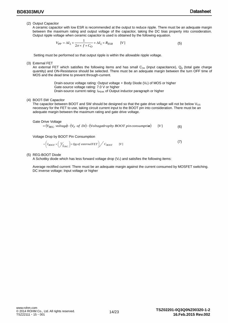
(2) Output Capacitor A ceramic capacitor with low ESR is recommended at the output to reduce ripple. There must be an adequate margin
between the maximum rating and output voltage of the capacitor, taking the DC bias property into consideration. Output ripple voltage when ceramic capacitor is used is obtained by the following equation.
(5)
Setting must be performed so that output ripple is within the allowable ripple voltage.
(3) External FET An external FET which satisfies the following items and has small Ciss (input capacitance), Qg (total gate charge quantity) and ON-Resistance should be selected. There must be an adequate margin between the turn OFF time of MOS and the dead time to prevent through-current.
Drain-source voltage rating: Output voltage + Body Diode (VF) of MOS or higher Gate-source voltage rating: 7.0 V or higher Drain-source current rating: IPEAK of Output inductor paragraph or higher
(4) BOOT-SW Capacitor The capacitor between BOOT and SW should be designed so that the gate drive voltage will not be below VGS necessary for the FET to use, taking circuit current input to the BOOT pin into consideration. There must be an adequate margin between the maximum rating and gate drive voltage.
Gate Drive Voltage
(6)
Voltage Drop by BOOT Pin Consumption
(7)
(5) REG-BOOT Diode A Schottky diode which has less forward voltage drop (VF) and satisfies the following items:
Average rectified current: There must be an adequate margin against the current consumed by MOSFET switching.
DC inverse voltage: Input voltage or higher
][2
1VRI
CfIV ESRL
OLPP
][VnconsumptiopinBOOTbydropVoltageDiofVvoltageV FREG
][1 VCFETexternalofQgf
I BOOTOSC
BOOT

15/23
BD8303MUV
© 2014 ROHM Co., Ltd. All rights reserved. www.rohm.com
TSZ22111・15・001
TSZ02201-0Q3Q0NZ00320-1-2
16.Feb.2015 Rev.002
(6) Setting of Oscillation Frequency Oscillation frequency can be set using a resistance value connected to the RT pin (Pin 1). Oscillation frequency is set at 600 kHz when RRT = 51kΩ, and frequency is inversely proportional to RT value (See Figure 25 for the relationship between RT and frequency) as a result, Soft-start time changes along with oscillation frequency (See Figure 26 for the relationship between RT and soft-start time)
(Note) Note that the above example of frequency setting is just a design target value, and may differ from the actual equipment.
(7) Output Voltage Setting
The internal reference voltage of the ERROR AMP is 1.0V. Output voltage should be obtained by referring to Equation (8) of Figure 27.
(8)
10
100
1000
10000
10 100 1000
RT PIN RESISTANCE [kΩ ]
SW
ITC
HN
G F
RE
QU
EN
CY
[kH
z]
1
10
100
10 100 1000
RT PIN RESISTANCE [kΩ ]
SO
FT
ST
AR
T T
IME
[m
sec]
Figure 25. Switching Frequency vs RT Pin Resistance Figure 26. Soft-Start Time vs RT Pin Resistance
VOUT
VREF 1.0V
ERROR AMP R1
R2
INV
Figure 27. Setting of Feedback Resistance
RT Pin Resistance [kΩ] RT Pin Resistance [kΩ]
Sw
itchin
g F
requency [kH
z]
Soft S
tart
Tim
e [m
sec]
][0.1
2
21 VR
RRVOUT

16/23
BD8303MUV
© 2014 ROHM Co., Ltd. All rights reserved. www.rohm.com
TSZ22111・15・001
TSZ02201-0Q3Q0NZ00320-1-2
16.Feb.2015 Rev.002
Figure 28. General Integrator
(8) Determination of External Phase Compensation Condition for stable application The condition for feedback system stability under negative feedback is as follows: Phase delay is 135 °or less when gain is 1 (0 dB) (Phase margin is 45° or higher). Since DC/DC converter application is sampled according to the switching frequency, the GBW of the whole system (frequency at which gain is 0 dB) must be set to be equal to or lower than 1/5 of the switching frequency.
(a) Phase delay must be 135°or lower when gain is 1 (0dB) (Phase margin is 45° or higher). (b) The GBW at that time (frequency when gain is 0 dB) must be equal to or lower than 1/5 of the switching
frequency. For this reason, switching frequency must be increased to improve responsiveness.
One of the points to secure stability by phase compensation is to cancel secondary phase delay (-180°) generated by LC resonance by the secondary phase lead (i.e. put two phase leads). Since Gain-BW is determined by the phase compensation capacitor attached to the error amplifier, when it is necessary to reduce Gain-BW, the capacitor should be made larger.
(9)
(10)
Phase compensation when output capacitor with low ESR such as ceramic capacitor is used is as follows: When output capacitor with low ESR (several tens of mΩ) is used for output, secondary phase lead (two phase leads) must be put to cancel secondary phase lead caused by LC. One of the examples of phase compensation methods is as follows:
(11)
(12)
(13)
(14)
Cout:Output Capacitor
For setting of phase-lead frequency, both of them should be put near LC resonance frequency. When GBW frequency becomes too high due to the secondary phase lead, it may get stabilized by putting the primary phase delay in a frequency slightly higher than the LC resonance frequency to compensate it.
Figure 29. Frequency Property of Integrator
-180°
0°
-90°
(A)
Phase margin
GAIN
[dB]
PHASE
[degree]
-20dB/decade
A
0 (B)
HzCR
fzleadPhase112
11
HzCR
fzleadPhase242
12
HzCR
fpdelayPhase132
11
][2
1)(int Hz
RCAfpAPo
][2
1)(int Hz
RCfBPo GBW
][
2
1Hz
LCoutfrequencyresonanceLC
FB R
C
+
-
FB
VOUT
C2 R1
R2
R3
R4 C1
Figure 30. Example of Setting of Phase Compensation
+
Error AMP is a low-pass filter because phase compensation such as (1) and (2) is performed. For DC/DC converter application, R is a parallel feedback resistance.
17/23
BD8303MUV
© 2014 ROHM Co., Ltd. All rights reserved. www.rohm.com
TSZ22111・15・001
TSZ02201-0Q3Q0NZ00320-1-2
16.Feb.2015 Rev.002
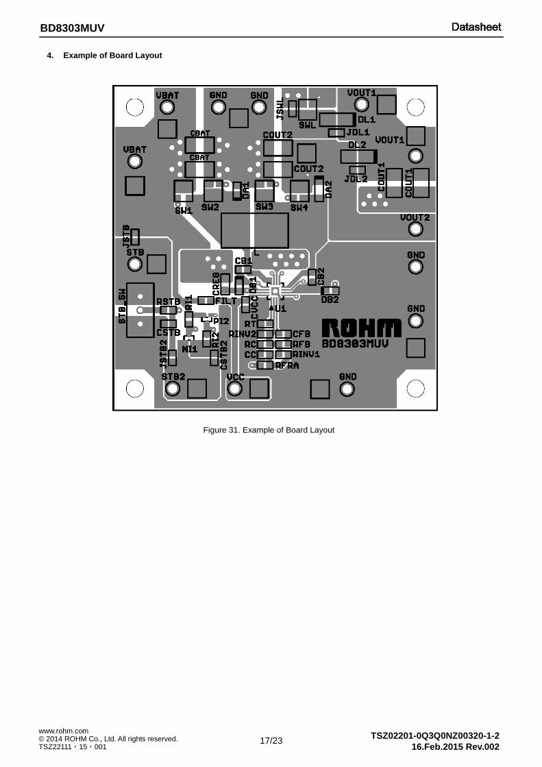
4. Example of Board Layout
Figure 31. Example of Board Layout

18/23
BD8303MUV
© 2014 ROHM Co., Ltd. All rights reserved. www.rohm.com
TSZ22111・15・001
TSZ02201-0Q3Q0NZ00320-1-2
16.Feb.2015 Rev.002
I/O Equivalent Circuits
RT
VREGVREG
RT
GND
STB
VCCVCC
GND
STB
LG1, LG2
PGND
VREG
PGND
LG1,2
VCC, REG GND
VCC
GND
VREG
FB
VREG
VREG
GND
FB
VREG
VREG
VREG
VREG
INV
VREGVREG
GND
INV
VREG
VREG
REG
REG
BOOT1 BOOT2 HG1, HG2 SW1, SW2
BOOT1,2
SW1,2
HG1,2
PGND
19/23
BD8303MUV
© 2014 ROHM Co., Ltd. All rights reserved. www.rohm.com
TSZ22111・15・001
TSZ02201-0Q3Q0NZ00320-1-2
16.Feb.2015 Rev.002
Operational Notes
1. Reverse Connection of Power Supply
Connecting the power supply in reverse polarity can damage the IC. Take precautions against reverse polarity when connecting the power supply, such as mounting an external diode between the power supply and the IC’s power supply pins.
2. Power Supply Lines
Design the PCB layout pattern to provide low impedance supply lines. Separate the ground and supply lines of the digital and analog blocks to prevent noise in the ground and supply lines of the digital block from affecting the analog block. Furthermore, connect a capacitor to ground at all power supply pins. Consider the effect of temperature and aging on the capacitance value when using electrolytic capacitors.
3. Ground Voltage
Ensure that no pins are at a voltage below that of the ground pin at any time, even during transient condition.
4. Ground Wiring Pattern
When using both small-signal and large-current ground traces, the two ground traces should be routed separately but connected to a single ground at the reference point of the application board to avoid fluctuations in the small-signal ground caused by large currents. Also ensure that the ground traces of external components do not cause variations on the ground voltage. The ground lines must be as short and thick as possible to reduce line impedance.
5. Thermal Consideration
Should by any chance the power dissipation rating be exceeded the rise in temperature of the chip may result in deterioration of the properties of the chip. In case of exceeding this absolute maximum rating, increase the board size and copper area to prevent exceeding the Pd rating.
6. Recommended Operating Conditions
These conditions represent a range within which the expected characteristics of the IC can be approximately obtained. The electrical characteristics are guaranteed under the conditions of each parameter.
7. Inrush Current
When power is first supplied to the IC, it is possible that the internal logic may be unstable and inrush current may flow instantaneously due to the internal powering sequence and delays, especially if the IC has more than one power supply. Therefore, give special consideration to power coupling capacitance, power wiring, width of ground wiring, and routing of connections.
8. Operation Under Strong Electromagnetic Field
Operating the IC in the presence of a strong electromagnetic field may cause the IC to malfunction.
9. Testing on Application Boards
When testing the IC on an application board, connecting a capacitor directly to a low-impedance output pin may subject the IC to stress. Always discharge capacitors completely after each process or step. The IC’s power supply should always be turned off completely before connecting or removing it from the test setup during the inspection process. To prevent damage from static discharge, ground the IC during assembly and use similar precautions during transport and storage.
10. Inter-pin Short and Mounting Errors
Ensure that the direction and position are correct when mounting the IC on the PCB. Incorrect mounting may result in damaging the IC. Avoid nearby pins being shorted to each other especially to ground, power supply and output pin. Inter-pin shorts could be due to many reasons such as metal particles, water droplets (in very humid environment) and unintentional solder bridge deposited in between pins during assembly to name a few.

20/23
BD8303MUV
© 2014 ROHM Co., Ltd. All rights reserved. www.rohm.com
TSZ22111・15・001
TSZ02201-0Q3Q0NZ00320-1-2
16.Feb.2015 Rev.002
Operational Notes – continued
11. Unused Input Pins
Input pins of an IC are often connected to the gate of a MOS transistor. The gate has extremely high impedance and extremely low capacitance. If left unconnected, the electric field from the outside can easily charge it. The small charge acquired in this way is enough to produce a significant effect on the conduction through the transistor and cause unexpected operation of the IC. So unless otherwise specified, unused input pins should be connected to the power supply or ground line.
12. Regarding the Input Pin of the IC
This monolithic IC contains P+ isolation and P substrate layers between adjacent elements in order to keep them isolated. P-N junctions are formed at the intersection of the P layers with the N layers of other elements, creating a parasitic diode or transistor. For example (refer to figure below):
When GND > Pin A and GND > Pin B, the P-N junction operates as a parasitic diode. When GND > Pin B, the P-N junction operates as a parasitic transistor.
Parasitic diodes inevitably occur in the structure of the IC. The operation of parasitic diodes can result in mutual interference among circuits, operational faults, or physical damage. Therefore, conditions that cause these diodes to operate, such as applying a voltage lower than the GND voltage to an input pin (and thus to the P substrate) should be avoided.
Figure 32. Example of monolithic IC structure
13. Thermal Shutdown Circuit(TSD)
This IC has a built-in thermal shutdown circuit that prevents heat damage to the IC. Normal operation should always be within the IC’s power dissipation rating. If however the rating is exceeded for a continued period, the junction temperature (Tj) will rise which will activate the TSD circuit that will turn OFF all output pins. When the Tj falls below the TSD threshold, the circuits are automatically restored to normal operation. Note that the TSD circuit operates in a situation that exceeds the absolute maximum ratings and therefore, under no circumstances, should the TSD circuit be used in a set design or for any purpose other than protecting the IC from heat damage.
N NP
+ P
N NP
+
P Substrate
GND
NP
+
N NP
+N P
P Substrate
GND GND
Parasitic
Elements
Pin A
Pin A
Pin B Pin B
B C
E
Parasitic
Elements
GNDParasitic
Elements
CB
E
Transistor (NPN)Resistor
N Region
close-by
Parasitic
Elements
21/23
BD8303MUV
© 2014 ROHM Co., Ltd. All rights reserved. www.rohm.com
TSZ22111・15・001
TSZ02201-0Q3Q0NZ00320-1-2
16.Feb.2015 Rev.002
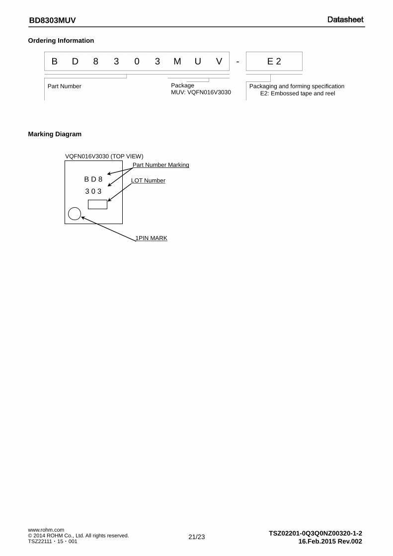
Ordering Information
Marking Diagram
B D 8 3 0 3 M U V - E 2
Part Number Package
MUV: VQFN016V3030 Packaging and forming specification
E2: Embossed tape and reel
VQFN016V3030 (TOP VIEW)
3 0 3
Part Number Marking
LOT Number
1PIN MARK
B D 8

22/23
BD8303MUV
© 2014 ROHM Co., Ltd. All rights reserved. www.rohm.com
TSZ22111・15・001
TSZ02201-0Q3Q0NZ00320-1-2
16.Feb.2015 Rev.002
Physical Dimension, Tape and Reel Information
Package Name VQFN016V3030
23/23
BD8303MUV
© 2014 ROHM Co., Ltd. All rights reserved. www.rohm.com
TSZ22111・15・001
TSZ02201-0Q3Q0NZ00320-1-2
16.Feb.2015 Rev.002
Revision History
Date Revision Changes
26.Nov.2014 001 New Release
16.Feb.2015 002 Correction of the writing.

DatasheetDatasheet
Notice-GE Rev.004© 2013 ROHM Co., Ltd. All rights reserved.
Notice Precaution on using ROHM Products
1. Our Products are designed and manufactured for application in ordinary electronic equipments (such as AV equipment, OA equipment, telecommunication equipment, home electronic appliances, amusement equipment, etc.). If you intend to use our Products in devices requiring extremely high reliability (such as medical equipment (Note 1), transport equipment, traffic equipment, aircraft/spacecraft, nuclear power controllers, fuel controllers, car equipment including car accessories, safety devices, etc.) and whose malfunction or failure may cause loss of human life, bodily injury or serious damage to property (“Specific Applications”), please consult with the ROHM sales representative in advance. Unless otherwise agreed in writing by ROHM in advance, ROHM shall not be in any way responsible or liable for any damages, expenses or losses incurred by you or third parties arising from the use of any ROHM’s Products for Specific Applications.
(Note1) Medical Equipment Classification of the Specific Applications JAPAN USA EU CHINA
CLASSⅢ CLASSⅢ
CLASSⅡb CLASSⅢ
CLASSⅣ CLASSⅢ
2. ROHM designs and manufactures its Products subject to strict quality control system. However, semiconductor
products can fail or malfunction at a certain rate. Please be sure to implement, at your own responsibilities, adequate safety measures including but not limited to fail-safe design against the physical injury, damage to any property, which a failure or malfunction of our Products may cause. The following are examples of safety measures:
[a] Installation of protection circuits or other protective devices to improve system safety [b] Installation of redundant circuits to reduce the impact of single or multiple circuit failure
3. Our Products are designed and manufactured for use under standard conditions and not under any special or extraordinary environments or conditions, as exemplified below. Accordingly, ROHM shall not be in any way responsible or liable for any damages, expenses or losses arising from the use of any ROHM’s Products under any special or extraordinary environments or conditions. If you intend to use our Products under any special or extraordinary environments or conditions (as exemplified below), your independent verification and confirmation of product performance, reliability, etc, prior to use, must be necessary:
[a] Use of our Products in any types of liquid, including water, oils, chemicals, and organic solvents [b] Use of our Products outdoors or in places where the Products are exposed to direct sunlight or dust [c] Use of our Products in places where the Products are exposed to sea wind or corrosive gases, including Cl2,
H2S, NH3, SO2, and NO2
[d] Use of our Products in places where the Products are exposed to static electricity or electromagnetic waves [e] Use of our Products in proximity to heat-producing components, plastic cords, or other flammable items [f] Sealing or coating our Products with resin or other coating materials [g] Use of our Products without cleaning residue of flux (even if you use no-clean type fluxes, cleaning residue of
flux is recommended); or Washing our Products by using water or water-soluble cleaning agents for cleaning residue after soldering
[h] Use of the Products in places subject to dew condensation
4. The Products are not subject to radiation-proof design. 5. Please verify and confirm characteristics of the final or mounted products in using the Products. 6. In particular, if a transient load (a large amount of load applied in a short period of time, such as pulse. is applied,
confirmation of performance characteristics after on-board mounting is strongly recommended. Avoid applying power exceeding normal rated power; exceeding the power rating under steady-state loading condition may negatively affect product performance and reliability.
7. De-rate Power Dissipation (Pd) depending on Ambient temperature (Ta). When used in sealed area, confirm the actual
ambient temperature. 8. Confirm that operation temperature is within the specified range described in the product specification. 9. ROHM shall not be in any way responsible or liable for failure induced under deviant condition from what is defined in
this document.
Precaution for Mounting / Circuit board design 1. When a highly active halogenous (chlorine, bromine, etc.) flux is used, the residue of flux may negatively affect product
performance and reliability.
2. In principle, the reflow soldering method must be used on a surface-mount products, the flow soldering method must be used on a through hole mount products. If the flow soldering method is preferred on a surface-mount products, please consult with the ROHM representative in advance.
For details, please refer to ROHM Mounting specification

DatasheetDatasheet
Notice-GE Rev.004© 2013 ROHM Co., Ltd. All rights reserved.
Precautions Regarding Application Examples and External Circuits 1. If change is made to the constant of an external circuit, please allow a sufficient margin considering variations of the
characteristics of the Products and external components, including transient characteristics, as well as static characteristics.
2. You agree that application notes, reference designs, and associated data and information contained in this document
are presented only as guidance for Products use. Therefore, in case you use such information, you are solely responsible for it and you must exercise your own independent verification and judgment in the use of such information contained in this document. ROHM shall not be in any way responsible or liable for any damages, expenses or losses incurred by you or third parties arising from the use of such information.
Precaution for Electrostatic
This Product is electrostatic sensitive product, which may be damaged due to electrostatic discharge. Please take proper caution in your manufacturing process and storage so that voltage exceeding the Products maximum rating will not be applied to Products. Please take special care under dry condition (e.g. Grounding of human body / equipment / solder iron, isolation from charged objects, setting of Ionizer, friction prevention and temperature / humidity control).
Precaution for Storage / Transportation 1. Product performance and soldered connections may deteriorate if the Products are stored in the places where:
[a] the Products are exposed to sea winds or corrosive gases, including Cl2, H2S, NH3, SO2, and NO2 [b] the temperature or humidity exceeds those recommended by ROHM [c] the Products are exposed to direct sunshine or condensation [d] the Products are exposed to high Electrostatic
2. Even under ROHM recommended storage condition, solderability of products out of recommended storage time period may be degraded. It is strongly recommended to confirm solderability before using Products of which storage time is exceeding the recommended storage time period.
3. Store / transport cartons in the correct direction, which is indicated on a carton with a symbol. Otherwise bent leads
may occur due to excessive stress applied when dropping of a carton. 4. Use Products within the specified time after opening a humidity barrier bag. Baking is required before using Products of
which storage time is exceeding the recommended storage time period.
Precaution for Product Label QR code printed on ROHM Products label is for ROHM’s internal use only.
Precaution for Disposition When disposing Products please dispose them properly using an authorized industry waste company.
Precaution for Foreign Exchange and Foreign Trade act Since our Products might fall under controlled goods prescribed by the applicable foreign exchange and foreign trade act, please consult with ROHM representative in case of export.
Precaution Regarding Intellectual Property Rights 1. All information and data including but not limited to application example contained in this document is for reference
only. ROHM does not warrant that foregoing information or data will not infringe any intellectual property rights or any other rights of any third party regarding such information or data. ROHM shall not be in any way responsible or liable for infringement of any intellectual property rights or other damages arising from use of such information or data.:
2. No license, expressly or implied, is granted hereby under any intellectual property rights or other rights of ROHM or any
third parties with respect to the information contained in this document.
Other Precaution 1. This document may not be reprinted or reproduced, in whole or in part, without prior written consent of ROHM. 2. The Products may not be disassembled, converted, modified, reproduced or otherwise changed without prior written
consent of ROHM. 3. In no event shall you use in any way whatsoever the Products and the related technical information contained in the
Products or this document for any military purposes, including but not limited to, the development of mass-destruction weapons.
4. The proper names of companies or products described in this document are trademarks or registered trademarks of
ROHM, its affiliated companies or third parties.

DatasheetDatasheet
Notice – WE Rev.001© 2015 ROHM Co., Ltd. All rights reserved.
General Precaution 1. Before you use our Pro ducts, you are requested to care fully read this document and fully understand its contents.
ROHM shall n ot be in an y way responsible or liabl e for fa ilure, malfunction or acci dent arising from the use of a ny ROHM’s Products against warning, caution or note contained in this document.
2. All information contained in this docume nt is current as of the issuing date and subj ect to change without any prior
notice. Before purchasing or using ROHM’s Products, please confirm the la test information with a ROHM sale s representative.
3. The information contained in this doc ument is provi ded on an “as is” basis and ROHM does not warrant that all
information contained in this document is accurate an d/or error-free. ROHM shall not be in an y way responsible or liable for any damages, expenses or losses incurred by you or third parties resulting from inaccuracy or errors of or concerning such information.