Embed Size (px)
Citation preview
J. Phys.: Condens. Matter10 (1998) 4785–4809. Printed in the UK PII: S0953-8984(98)90099-6
Low frequency plasmons in thin-wire structures
J B Pendry†, A J Holden‡, D J Robbins‡ and W J Stewart‡† The Blackett Laboratory, Imperial College, London SW7 2BZ, UK‡ GEC–Marconi Materials Technology Ltd, Caswell, Towcester, Northamptonshire NN12 8EQ,UK
Received 16 December 1997, in final form 20 March 1998
Abstract. A photonic structure consisting of an extended 3D network of thin wires is shownto behave like a low density plasma of very heavy charged particles with a plasma frequencyin the GHz range. We show that the analogy with metallic behaviour in the visible is rathercomplete, and the picture is confirmed by three independent investigations: analytic theory,computer simulation and experiments on a model structure. The fact that the wires are thin iscrucial to the validity of the picture. This new composite dielectric, which has the property ofnegativeε below the plasma frequency, opens new possibilities for GHz devices.
1. Introduction
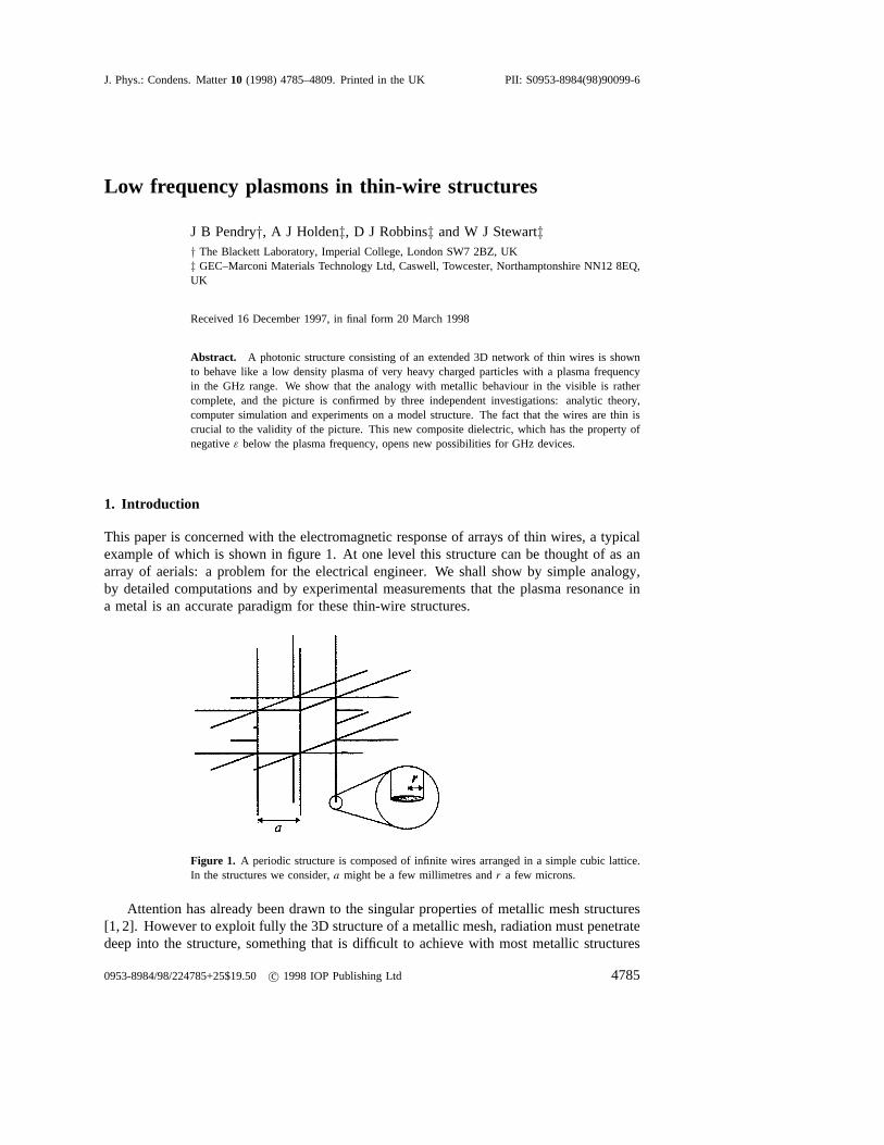
This paper is concerned with the electromagnetic response of arrays of thin wires, a typicalexample of which is shown in figure 1. At one level this structure can be thought of as anarray of aerials: a problem for the electrical engineer. We shall show by simple analogy,by detailed computations and by experimental measurements that the plasma resonance ina metal is an accurate paradigm for these thin-wire structures.
Figure 1. A periodic structure is composed of infinite wires arranged in a simple cubic lattice.In the structures we consider,a might be a few millimetres andr a few microns.
Attention has already been drawn to the singular properties of metallic mesh structures[1, 2]. However to exploit fully the 3D structure of a metallic mesh, radiation must penetratedeep into the structure, something that is difficult to achieve with most metallic structures
0953-8984/98/224785+25$19.50c© 1998 IOP Publishing Ltd 4785

4786 J B Pendry et al
whose properties simply reduce to those of a 2D grating. In our earlier paper [2] wepointed out the significance of choosing thin wires, which reduces the interaction of radiationsufficiently to allow penetration and to bring into play the 3D properties of the mesh.
Intense interest has been shown in periodic electromagnetic structures since thedemonstration of a photonic band gap by Yablonovitchet al [3]: see [4, 5] for recentreviews. However most of the attention has been concentrated on dielectric structures.Metallic structures have been considered in a very different context: energy loss in theelectron microscope [6–10]. Here it has been known for some time that the structure ofmetallic objects, such as arrays of colloidal spheres, profoundly affects the loss spectrum.This happens primarily through the metallic surface plasma modes [11, 12] which couplevery strongly to incident charged particles [13]. If the surfaces are not flat there is alsostrong coupling to incident transverse modes.
Metals have a characteristic response to electromagnetic radiation due to the plasmaresonance of the electron gas [14, 15]. Ideally they are described by a dielectric function ofthe form
εmetal = 1− ω2p
ω2(1)
where the plasma frequency,ωp, is given in terms of the electron density,n, the electronmass,me, and charge,e,
ω2p =
ne2
ε0me. (2)
Equation (1) implies a dispersion relation shown in figure 2.
Figure 2. Characteristic dispersion relationship for light in an ideal metal. Two degeneratetransverse modes emerge at the plasma frequency and asymptotically approach the free lightcone. A singly degenerate longitudinal plasma mode shows no dispersion. Only evanescentmodes (imaginary wave vector) exist below the plasma frequency.
A longitudinal mode, the plasmon, appears at a fixed frequency, and two longitudinalmodes emerge at the plasma frequency. In consequence of the negativeε, only evancescentmodes (imaginary wave vector) exist below the plasma frequency and below this thresholdno radiation penetrates very far into the metal. In a normal metal the ideal form is spoiltby the resistance which introduces damping,
εnormal = 1− ω2p
ω(ω + iγ ). (3)
Low frequency plasmons in thin-wire structures 4787
Typically γ becomes significant in the infra-red. However for a superconductor thecondensate continues to display the ideal behaviour and we can, in fact, calculate theLondon penetration depth from (1).
Much has been made of this dispersion relationship which for the transverse modesis reminiscent of a relativistic massive particle. In particular, Anderson [16] has pointedout that the acquisition of mass, along with the appearance of the dispersionless (i.e. verymassive) plasmon, is an example of the Higgs phenomenon. It certainly imparts someunique qualities to metals: their ability to exclude light, the very strong interaction withcharged particles, and the curious resonant modes that appear on the surface of a metalin consequence of the negativeε below ωp. The modes may couple to incident radiationprovided that the surface is not completely flat, and often give a strong resonant responseas in the surface enhanced Raman scattering seen at rough silver surfaces.
Our motivation is to fabricate composite materials that replicate the characteristicfeatures of metallic response to radiation, but in the GHz range of frequencies rather thanin the visible. We are particularly interested in the property of negativeε, which is not seenin any naturally occurring materials at these frequencies.
We shall first show that a simple analytic argument rapidly develops the plasma analogy.Then we make some more serious calculations by solving Maxwell’s equations on acomputer and confirming that the simply theory works surprisingly well: quantitativeagreement at the 5% level is seen. Next we present experimental data from a thin-wirestructure manufactured using spark chamber technology borrowed from high energy physics,and show that this confirms our plasma model with good accuracy, again around the 5%level. Finally, the theory confirmed by experiment, we use the computer to explore variationsof the model and show that it is robust under variations in the wire structure: the essentialrequirements are simply that we have a three dimensional array of thincontinuouswires.
2. An approximate analytic theory
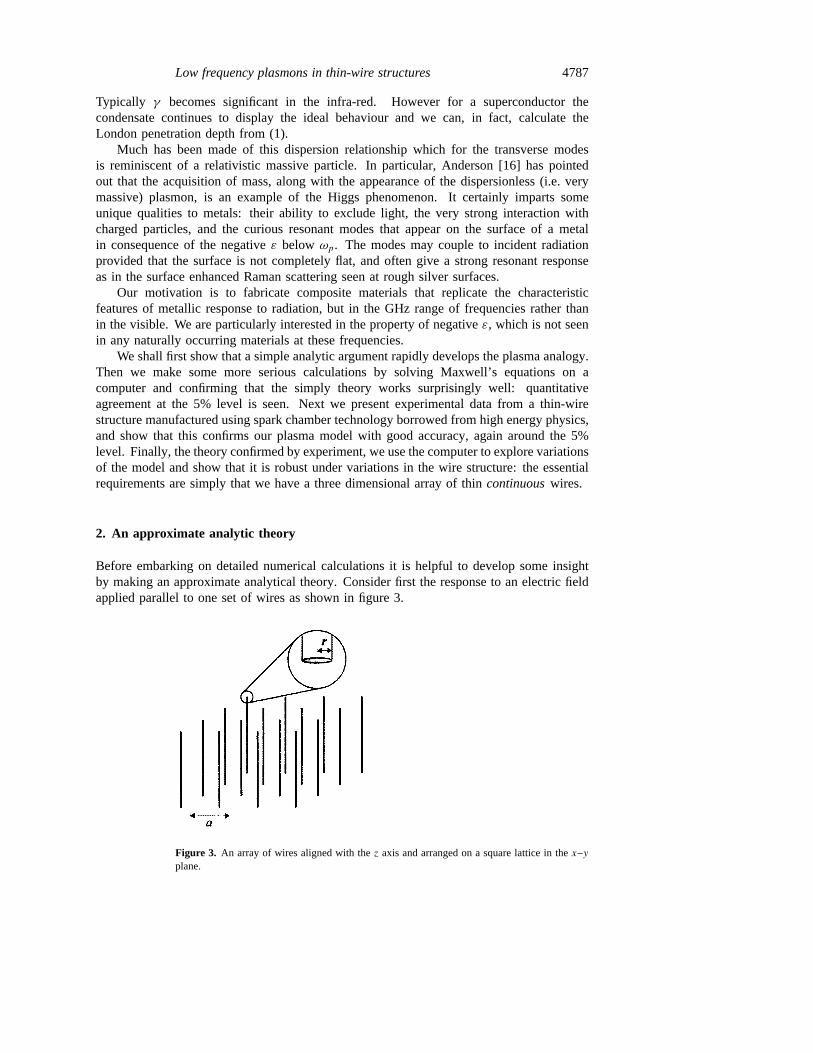
Before embarking on detailed numerical calculations it is helpful to develop some insightby making an approximate analytical theory. Consider first the response to an electric fieldapplied parallel to one set of wires as shown in figure 3.
Figure 3. An array of wires aligned with thez axis and arranged on a square lattice in thex–yplane.
4788 J B Pendry et al
Constraining electrons to move along thin wires has two consequences.The first is that average electron density is reduced because only part of the space is
filled by metal,
neff = nπr2
a2(4)
wheren is the density of electrons in the wires themselves,r is the radius of the wire anda is the cell side of the square lattice on which the wires are arranged.
The second is an enhancement of the effective mass of the electrons caused by magneticeffects. When any current flows a strong magnetic field is established around the wire givenby
H(R) = I
2πR= πr2nve
2πR(5)
whereI is the current flowing in the wire,R is the distance from the wire andv is themean electron velocity. We can express this field as,
H(R) = µ−10 ∇×A (6)
where
A(R) = µ0πr2nve
2πln(a/R) (7)
anda is the lattice constant. We shall justify this formula below.We note that, from classical mechanics, electrons in a magnetic field have an additional
contribution to their momentum ofeA, and therefore the momentum per unit length of thewire is
eπr2nA(r) = µ0e2(πr2n)2v
2πln(a/r) = meff πr2nv (8)
wheremeff is the new effective mass of the electrons given by
meff = µ0e2πr2n
2πln(a/r). (9)
Inserting the following values,
r = 1.0× 10⁻⁶ m a = 5 mm
n = 1.806× 1029 m−3 (aluminium) (10)
gives a mass of
meff = 2.4808× 10⁻²⁶ kg= 2.7233× 10⁴ me = 14.83mp (11)
whereme is the electron mass andmp the proton mass. This is an enormously enhancedeffective mass and shifts the plasma frequency by a correspondingly large amount. Fromthe classical formula for the plasma frequency,
ω2p =
neff e2
ε0meff= 2πc2
0
a2 ln(a/r)(12)
wherec0 is the velocity of light in free space. Substituting gives
ωp = 5.15× 10¹⁰ rad s−1 = 8.20 GHz (13)
in excellent agreement with the computational estimate of 8.3 GHz which we shall makein the next section.

Low frequency plasmons in thin-wire structures 4789
Using equation (12) we can show the importance of thin wires. Supposing that thewires were not thin so that we could neglect ln(a/r). Then the free space wavelength atthe plasma frequency is
λ0p = 2πc0
ωp≈ a√
2π. (14)
In other words without the effect of thin wiresλ0p is of the same order as the lattice constantproducing diffraction effects which confuse our simple picture. Furthermore if we calculatethe penetration depth at, say, half the plasma frequency,
penetration depth= a√
2 ln(a/r)
3π(15)
we can see than without the thin-wire effect radiation hardly penetrates the lattice at all.Now let us justify the formula quoted forA in equation (7). Suppose that we have a
plasmon-like longitudinal excitation in the system shown in figure 3, wave vector parallelto thez axis, with wavelength much longer than the lattice period,a.
D = [0, 0,D0] exp[i(kz− ωt)]. (16)
Next we calculate the associated magnetic field from
∇×H = ∂D
∂t+ j. (17)
Note that if bothD andj have the same distribution in thex–y plane, then the right-handside of the above equation vanishes and hence the magnetic field is zero. We can see this bycalculating the accompanying charge and current density implied by the longitudinal field,
σ =∇ ·D = ikD0 exp[i(kz− ωt)]j = iω[0, 0,D0] exp[i(kz− ωt)]. (18)
Hence on substituting into (17) the two contributions vanish. This is what happens insidea capacitor discharging through a uniform dielectric filling: no magnetic field is generated.
In our caseD and j have different distributions in thex–y plane. The current isconfined to the very thin wires whereas in the limit of long wavelengthD is uniform in thex–y plane. Hence in our case the magnetic field is non-zero and, as we shall show, happensto be large close to the wire. Divide thex–y plane into square unit cells each centred on awire. On average each cell has zero source with respect to the magnetic field. To calculatethe magnetic field we make the approximation of replacing each square cell with a circleof the same area and having a uniform distribution ofD just like the square. The radiusof the circle is
Rc = a/√π. (19)
At a given point in thex–y plane the magnetic field only has contributions from the circleinside whose circumference it lies. All other circles have zero contribution. We can easilycalculate the magnetic field inside the circle,
Hc = j
2πR− j
2πR
R2
R2c
0< R < Rc
= 0 r > Rc
(20)
and the corresponding vector potential points along thez axis and has magnitude
Ac(R) = µ0j
2π
[ln
(R
Rc
)− R
2− R2c
2R2c
]0< R < Rc
= 0 R > Rc
(21)
4790 J B Pendry et al
where we have exploited our freedom to choose the constant of integration so thatA iszero outside the circle. The point of making this particular choice is that theA vector ofone circle does not overlap with the centre of another and therefore the mutual inductancebetween the wires has been addressed, at least in this approximation. It only remains toevaluate theA vector at the wire,
Ac(r) = µ0j
2π
[ln
(r
Rc
)− r
2− R2c
2R2c
]= µ0j
2π
[ln
(r√π
a
)− πr
2
2a2+ 1
2
]. (22)
Since in our example,
ln( ra
)= ln
(10−6
5× 10⁻³
)= −8.5 (23)
it is a good approximation to take
Ac(r) ≈ µ0j
2πln( ra
)(24)
as we quoted above.Corrections to the circle approximation are very small because the square cells already
have fourfold symmetry and therefore the residual magnetic field will fall off asR−4.
3. Solving Maxwell’s equations—numerical simulations
Standard codes exist for the calculation of electromagnetic properties of structured materials[17–19]. They function by dividing space into a mesh of points on which the fields aresampled: typically a uniform mesh is used for simplicity. The problem for thin-wirestructures is that a uniform mesh makes an extremely poor sampling of the intense fieldsnear to the wire unless an unacceptably large number of points is used. Otherwise a complexnon-uniform mesh needs to be constructed. Fortunately we can avoid both unpleasantalternatives by a simple trick.
The only interest we have in the response of the wires is in the external fields they createfar from the wires. Therefore if the thin wires are replaced by thicker wires which haveexactly the same external effect, the electromagnetic response will be unaffected. Howevera thick wire with a relatively uniform distribution of field and current will be much moreeasily sampled by a uniform mesh than the original thin wire.
3.1. The equivalent conductance of fibres
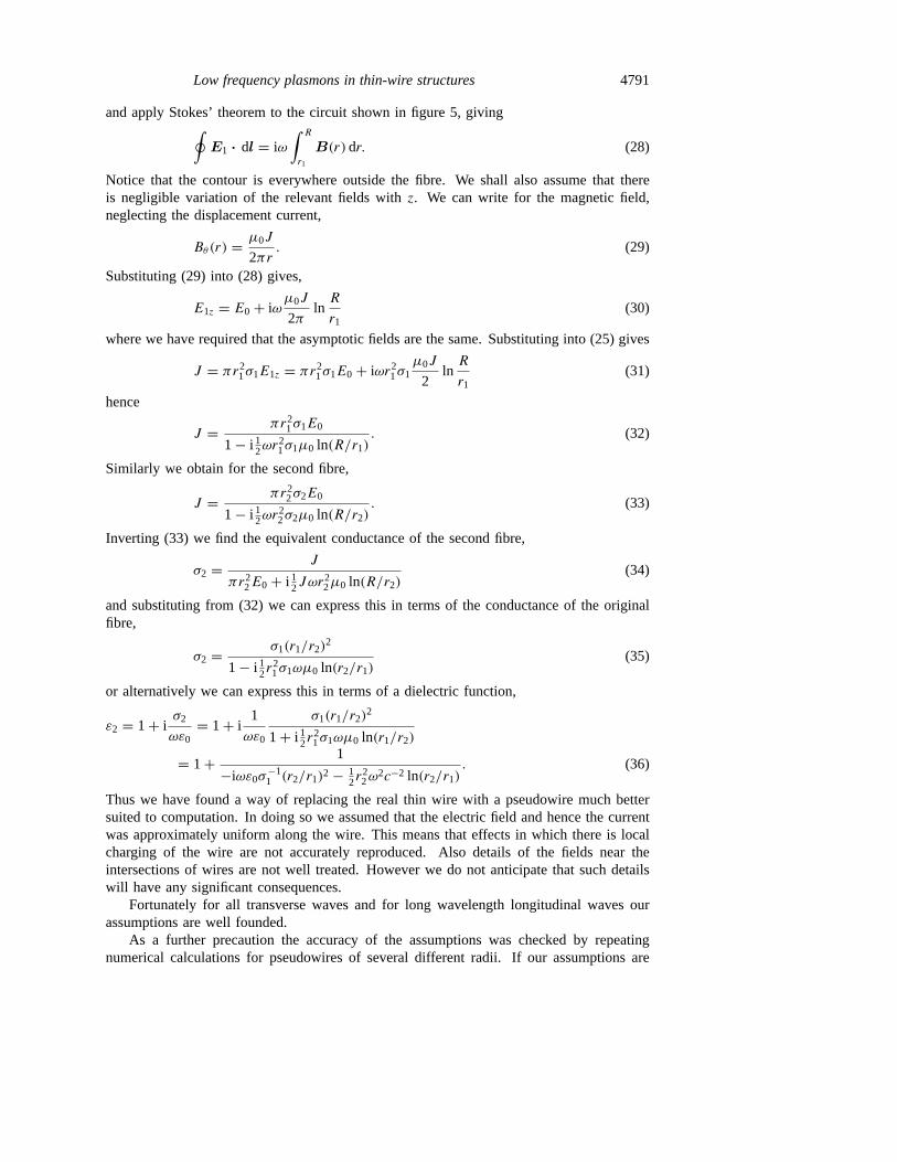
The objective is to take a wire of small radius in a set of external fields, and replace it withan equivalent fibre of larger radius which has the same external fields (see figure 4). Thekey quantity will be the current flowing along the length of the wire,J , which we assumeto be uniformly distributed over the cross section of the fibre: true if the wire is very thin.This determines the local external magnetic field and therefore must take the same value inboth fibres. We calculate the current from the conductance of the wire,
J = πr21σ1E1z (25)
J = πr22σ2E2z. (26)
Ez has two components: a far-field external component, and a near-field inductive one.First we relate the near fieldEz to the magnetic field, then we relate the magnetic field toJ and require self-consistency. We start from
∇×E = +iωB (27)
Low frequency plasmons in thin-wire structures 4791
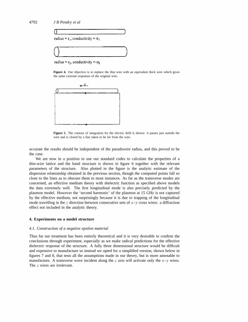
and apply Stokes’ theorem to the circuit shown in figure 5, giving∮E1 · dl = iω
∫ R
r1
B(r) dr. (28)
Notice that the contour is everywhere outside the fibre. We shall also assume that thereis negligible variation of the relevant fields withz. We can write for the magnetic field,neglecting the displacement current,
Bθ(r) = µ0J
2πr. (29)
Substituting (29) into (28) gives,
E1z = E0+ iωµ0J
2πlnR
r1(30)
where we have required that the asymptotic fields are the same. Substituting into (25) gives
J = πr21σ1E1z = πr2
1σ1E0+ iωr21σ1
µ0J
2lnR
r1(31)
hence
J = πr21σ1E0
1− i 12ωr
21σ1µ0 ln(R/r1)
. (32)
Similarly we obtain for the second fibre,
J = πr22σ2E0
1− i 12ωr
22σ2µ0 ln(R/r2)
. (33)
Inverting (33) we find the equivalent conductance of the second fibre,
σ2 = J
πr22E0+ i 1
2Jωr22µ0 ln(R/r2)
(34)
and substituting from (32) we can express this in terms of the conductance of the originalfibre,
σ2 = σ1(r1/r2)2
1− i 12r
21σ1ωµ0 ln(r2/r1)
(35)
or alternatively we can express this in terms of a dielectric function,
ε2 = 1+ iσ2
ωε0= 1+ i
1
ωε0
σ1(r1/r2)2
1+ i 12r
21σ1ωµ0 ln(r1/r2)
= 1+ 1
−iωε0σ−11 (r2/r1)2− 1
2r22ω
2c−2 ln(r2/r1). (36)
Thus we have found a way of replacing the real thin wire with a pseudowire much bettersuited to computation. In doing so we assumed that the electric field and hence the currentwas approximately uniform along the wire. This means that effects in which there is localcharging of the wire are not accurately reproduced. Also details of the fields near theintersections of wires are not well treated. However we do not anticipate that such detailswill have any significant consequences.
Fortunately for all transverse waves and for long wavelength longitudinal waves ourassumptions are well founded.
As a further precaution the accuracy of the assumptions was checked by repeatingnumerical calculations for pseudowires of several different radii. If our assumptions are
4792 J B Pendry et al
Figure 4. Our objective is to replace the thin wire with an equivalent thick wire which givesthe same external responses of the original wire.
Figure 5. The contour of integration for the electric field is shown: it passes just outside thewire and is closed by a line taken to be far from the wire.
accurate the results should be independent of the pseudowire radius, and this proved to bethe case.
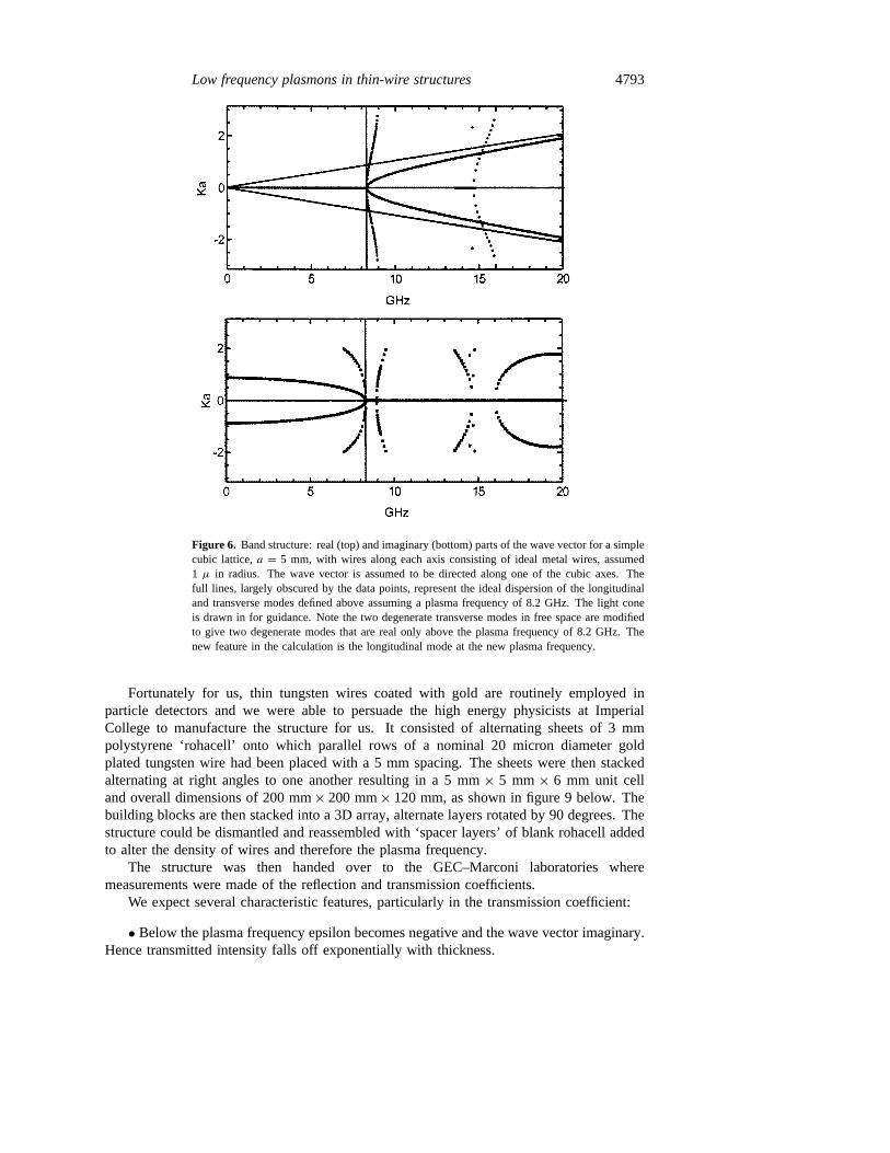
We are now in a position to use our standard codes to calculate the properties of athin-wire lattice and the band structure is shown in figure 6 together with the relevantparameters of the structure. Also plotted in the figure is the analytic estimate of thedispersion relationship obtained in the previous section, though the computed points fall soclose to the lines as to obscure them in most instances. As far as the transverse modes areconcerned, an effective medium theory with dielectric function as specified above modelsthe data extremely well. The first longitudinal mode is also precisely predicted by theplasmon model. However the ‘second harmonic’ of the plasmon at 15 GHz is not capturedby the effective medium, not surprisingly because it is due to trapping of the longitudinalmode travelling in thez direction between consecutive sets ofx–y cross wires: a diffractioneffect not included in the analytic theory.
4. Experiments on a model structure
4.1. Construction of a negative epsilon material
Thus far our treatment has been entirely theoretical and it is very desirable to confirm theconclusions through experiment, especially as we make radical predictions for the effectivedielectric response of the structure. A fully three dimensional structure would be difficultand expensive to manufacture so instead we opted for a simplified version, shown below infigures 7 and 8, that tests all the assumptions made in our theory, but is more amenable tomanufacture. A transverse wave incident along thez axis will activate only thex–y wires.The z wires are irrelevant.
Low frequency plasmons in thin-wire structures 4793
Figure 6. Band structure: real (top) and imaginary (bottom) parts of the wave vector for a simplecubic lattice,a = 5 mm, with wires along each axis consisting of ideal metal wires, assumed1 µ in radius. The wave vector is assumed to be directed along one of the cubic axes. Thefull lines, largely obscured by the data points, represent the ideal dispersion of the longitudinaland transverse modes defined above assuming a plasma frequency of 8.2 GHz. The light coneis drawn in for guidance. Note the two degenerate transverse modes in free space are modifiedto give two degenerate modes that are real only above the plasma frequency of 8.2 GHz. Thenew feature in the calculation is the longitudinal mode at the new plasma frequency.
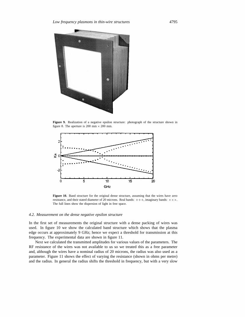
Fortunately for us, thin tungsten wires coated with gold are routinely employed inparticle detectors and we were able to persuade the high energy physicists at ImperialCollege to manufacture the structure for us. It consisted of alternating sheets of 3 mmpolystyrene ‘rohacell’ onto which parallel rows of a nominal 20 micron diameter goldplated tungsten wire had been placed with a 5 mmspacing. The sheets were then stackedalternating at right angles to one another resulting in a 5 mm× 5 mm× 6 mm unit celland overall dimensions of 200 mm× 200 mm× 120 mm, as shown in figure 9 below. Thebuilding blocks are then stacked into a 3D array, alternate layers rotated by 90 degrees. Thestructure could be dismantled and reassembled with ‘spacer layers’ of blank rohacell addedto alter the density of wires and therefore the plasma frequency.
The structure was then handed over to the GEC–Marconi laboratories wheremeasurements were made of the reflection and transmission coefficients.
We expect several characteristic features, particularly in the transmission coefficient:
• Below the plasma frequency epsilon becomes negative and the wave vector imaginary.Hence transmitted intensity falls off exponentially with thickness.

4794 J B Pendry et al
Figure 7. Realization of a negative epsilon structure. Thin gold plated tungsten wires, nominally20 microns in diameter, are laid in parallel rows onto polystyrene sheets and built into thestructure shown above. The aperture is 200 mm× 200 mm.
Figure 8. Realization of a negative epsilon structure. Thin gold plated tungsten wires, nominally20 microns in diameter, are laid in parallel rows onto polystyrene sheets and built into thestructure shown above. The aperture is 200 mm× 200 mm.
• Below the plasma frequency there is no variation of phase as the wave crosses thesample because the wave vector is imaginary.• Above the plasma frequency the wave vector becomes real and the transmission
coefficient grows rapidly to of the order of unity. The rate at which the transmission risesis a measure of how resistive the wires are.• At the same time the phase starts to vary with frequency in a manner which reveals
the underlying dispersion ofk(ω).• A less pronounced feature in both transmission and reflection coefficients will be
the Fabry–Perot resonances which arise from multiple reflections of the wave within thestructure.
Low frequency plasmons in thin-wire structures 4795
Figure 9. Realization of a negative epsilon structure: photograph of the structure shown infigure 8. The aperture is 200 mm× 200 mm.
Figure 10. Band structure for the original dense structure, assuming that the wires have zeroresistance, and their stated diameter of 20 microns. Real bands:+++, imaginary bands:×××.The full lines show the dispersion of light in free space.
4.2. Measurement on the dense negative epsilon structure
In the first set of measurements the original structure with a dense packing of wires wasused. In figure 10 we show the calculated band structure which shows that the plasmaedge occurs at approximately 9 GHz; hence we expect a threshold for transmission at thisfrequency. The experimental data are shown in figure 11.
Next we calculated the transmitted amplitudes for various values of the parameters. TheRF resistance of the wires was not available to us so we treated this as a free parameterand, although the wires have a nominal radius of 20 microns, the radius was also used as aparameter. Figure 11 shows the effect of varying the resistance (shown in ohms per metre)and the radius. In general the radius shifts the threshold in frequency, but with a very slow
4796 J B Pendry et al
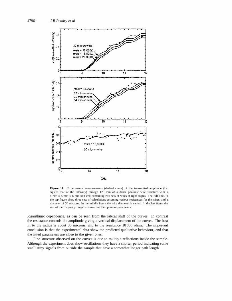
Figure 11. Experimental measurements (dashed curve) of the transmitted amplitude (i.e.square root of the intensity) through 120 mm of a dense photonic wire structure with a5 mm× 5 mm× 6 mm unit cell containing two sets of wires at right angles. The full lines inthe top figure show three sets of calculations assuming various resistances for the wires, and adiameter of 30 microns. In the middle figure the wire diameter is varied. In the last figure therest of the frequency range is shown for the optimum parameters.
logarithmic dependence, as can be seen from the lateral shift of the curves. In contrastthe resistance controls the amplitude giving a vertical displacement of the curves. The bestfit to the radius is about 30 microns, and to the resistance 18 000 ohms. The importantconclusion is that the experimental data show the predicted qualitative behaviour, and thatthe fitted parameters are close to the given ones.
Fine structure observed on the curves is due to multiple reflections inside the sample.Although the experiment does show oscillations they have a shorter period indicating somesmall stray signals from outside the sample that have a somewhat longer path length.

Low frequency plasmons in thin-wire structures 4797
Having fitted the parameters in the vicinity of the threshold we calculated thetransmission coefficient for the higher range of frequencies and compared to experiment.Note that if we ignore the high frequency oscillations due to spurious reflections, theagreement of absolute amplitudes is good.
Next we compared the calculated and measured phases in figure 12. Assuming that mostof the contribution to the transmitted amplitude arises from direct transmission through thesample without multiple scattering, the phase will be given by
φ = k(ω)d (37)
whered is the thickness of the sample: 120 mm in this instance. Therefore the phase is adirect measurement of the dispersion relationshipk(ω) to which it is very sensitive becauseof the relatively large value ofd. Below threshold at 9 GHz the phase is not well defined inthe experiment, presumably because of spurious reflections. Above threshold agreement isexcellent: between 9 and 18 GHz the phase scans though a range of approximately 6×360◦
with an error of around 3%.
4.3. Measurement on the double period negative epsilon structure
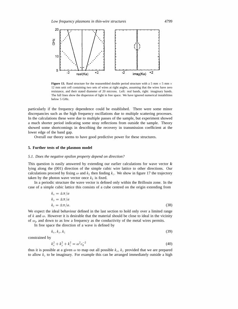
Having completed measurements on the dense structure, it was dismantled and reassembledto the same thickness of 120 mm but interspersing each wire sheet with a blank polystyrenesheet. The effect of diluting the wires is to reduce the threshold for transmission as can beseen from the band structure shown in figure 13.
Some numerical instability creeps into the calculations at low frequencies but the keypoint is the threshold which has now moved down from 9 to 6 GHz as a consequence ofthe sparser distribution of wires. Additionally we see at higher frequencies around 14 GHza band gap induced by Bragg scattering from the periodic wire structure. In this frequencyrange we expect a reduced transmission coefficient details of which can be used further tosupport our theoretical treatment.
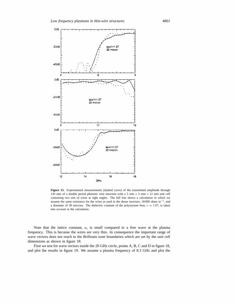
In figure 14 we show the calculated transmitted amplitude. Since we have alreadydetermined the wire parameters we should find that the same parameters fit for the doubleperiod structure. The previous calculations did not take account of the dielectric constantof the polystyrene sheets. Figure 14 shows that its effect near threshold at 6 GHz is almostcompletely compensated for by varying the diameter of the wires. However at higherfrequencies of 14 GHz, near the band gap where the transmission coefficient takes a dip,the wire diameter is much less important than the dielectric constant.
Comparing calculations to experiment gives a best fit with a diameter of 30 microns asbefore, andε = 1.07, though the latter parameter is probably only just distinguished fromunity. The best fit calculations are compared to experiment in figure 15. The threshold at6 GHz is very well reproduced. The band gap for the most part is well reproduced. Thereduction in intensity at the centre of the gap is confirmation that we have calculated thecorrect imaginary wave vector which in turn measures the interaction of the wave with thewire structure at these higher frequencies.
One slightly surprising discrepancy is the disagreement between 11 and 12 GHz whereexperiment shows 10 dB less transmission than the calculation. These frequencies are justbelow the band gap. There is a less pronounced disagreement just above the band gap. Itcould be that the RF resistance of the wires is greater than at lower frequencies leading toincreased loss in transmission.
Next the transmitted phases were compared in figure 16. Once again, below the thresholdat 6 GHz, the phase is ill defined because the transmitted intensity is so small. However from

4798 J B Pendry et al
Figure 12. Experimental measurements (dashed curve) of the phase transmitted through 120 mmof a photonic wire structure with a 5 mm×5 mm×6 mm unit cell containing two sets of wiresat right angles. The random jumps in phase ofπ are due to small measurement noise. Thefull lines show a calculation assuming a resistance of 18 000 ohms m−1 for the wires, and adiameter of 30 microns.
the threshold upwards to the beginning of the band gap at 12 GHz there is good agreement.Through the gap itself there is an interesting hiccup which is mostly reproduced, but againthe lower side of the gap is a region where agreement is less than perfect indicating theneed for some further fine tuning of parameters.
4.4. Conclusions on comparison to experiment
The most important conclusion is confirmation from experiment of the qualitative feature ofnegative epsilon below a threshold frequency, as evidenced by the cut-off in transmission.In addition we appear to be able to make quantitative predictions for the system, at least atthe 5% level of accuracy. The main uncertainty here is the RF resistance of the wire whichwas fitted to experiment. Independent confirmation of the value used would be helpful
Low frequency plasmons in thin-wire structures 4799
Figure 13. Band structure for the reassembled double period structure with a 5 mm× 5 mm×12 mm unit cell containing two sets of wires at right angles, assuming that the wires have zeroresistance, and their stated diameter of 20 microns. Left: real bands, right: imaginary bands.The full lines show the dispersion of light in free space. We have ignored numerical instabilitiesbelow 5 GHz.
particularly if the frequency dependence could be established. There were some minordiscrepancies such as the high frequency oscillations due to multiple scattering processes.In the calculations these were due to multiple passes of the sample, but experiment showeda much shorter period indicating some stray reflections from outside the sample. Theoryshowed some shortcomings in describing the recovery in transmission coefficient at thelower edge of the band gap.
Overall our theory seems to have good predictive power for these structures.
5. Further tests of the plasmon model
5.1. Does the negative epsilon property depend on direction?
This question is easily answered by extending our earlier calculations for wave vectorklying along the (001) direction of the simple cubic wire lattice to other directions. Ourcalculations proceed by fixingω andk‖ then findingkz. We show in figure 17 the trajectorytaken by the photon wave vector oncek‖ is fixed.
In a periodic structure the wave vector is defined only within the Brillouin zone. In thecase of a simple cubic lattice this consists of a cube centred on the origin extending from
kx = ±π/aky = ±π/akz = ±π/a. (38)
We expect the ideal behaviour defined in the last section to hold only over a limited rangeof k andω. However it is desirable that the material should be close to ideal in the vicinityof ωp and down to as low a frequency as the conductivity of the metal wires permits.
In free space the direction of a wave is defined by
kx, ky, kz (39)
constrained by
k2x + k2
y + k2z = ω2c−2
0 (40)
thus it is possible at a givenω to map out all possiblekx , ky provided that we are preparedto allow kz to be imaginary. For example this can be arranged immediately outside a high

4800 J B Pendry et al
Figure 14. Calculated transmitted amplitude (i.e. square root of the intensity) through 120 mmof a double period photonic wire structure with a 5 mm× 5 mm× 12 mm unit cell containingtwo sets of wires at right angles. We assume the same resistance for the wires as used in thedense structure, 18 000 ohms m−1. Two diameters are used, 20 microns and 30 microns, andthe dielectric constant of the polystyrene host,ε = 1.07, is taken into account in two of thecalculations.
refractive index material where an evanescent wave may decay strongly into the vacuum.However we suppose that in most practical situations we shall be confined to situations wherekx , ky , kz are all real thus limiting the range of values which they make take. In figure 18we show the range of wave vectors allowed for frequencies up to 20 GHz, approximatelytwice the plasma frequency, and we shall be content if the ideal model holds within thiscircle.
Low frequency plasmons in thin-wire structures 4801
Figure 15. Experimental measurements (dashed curve) of the transmitted amplitude through120 mm of a double period photonic wire structure with a 5 mm× 5 mm× 12 mm unit cellcontaining two sets of wires at right angles. The full line shows a calculation in which weassume the same resistance for the wires as used in the dense structure, 18 000 ohms m−1, anda diameter of 30 microns. The dielectric constant of the polystyrene host,ε = 1.07, is takeninto account in the calculation.
Note that the lattice constant,a, is small compared to a free wave at the plasmafrequency. This is because the wires are very thin. In consequence the important range ofwave vectors does not reach to the Brillouin zone boundaries which are set by the unit celldimensions as shown in figure 18.
First we test for wave vectors inside the 20 GHz circle, points A, B, C and D in figure 18,and plot the results in figure 19. We assume a plasma frequency of 8.3 GHz and plot the

4802 J B Pendry et al
Figure 16. Experimental measurements (dashed curve) of the phase transmitted through 120 mmof a photonic wire structure with a 5 mm×5 mm×12 mm unit cell containing two sets of wiresat right angles. The full lines show a calculation assuming a resistance of 18 000 ohms m−1 forthe wires, and a diameter of 30 microns and correspond to the amplitudes shown in figure 15.
dispersion of the longitudinal and transverse modes using this single parameter,
ω2 = c20k
2x + c2
0k2y + c2
0k2z + ω2
p (41)
and compare with our computations.Thus in the range of parameters within which we are concerned to test our theory, the
computed data fit the model very well: the longitudinal mode is dispersion free to within10% or 20% indicating thatε is indeed essentially independent ofk, and the transversemodes are also well reproduced.

Low frequency plasmons in thin-wire structures 4803
Figure 17. Our programs calculate the band structure,kz, for fixed ω andk‖ as shown in thissketch.
Figure 18. The photon wave vector projected onto the (001) surface Brillouin zone. The circleshows the magnitude of the wave vector for a 20 GHz photon. The band structure in figure 6is calculated for wave vectors perpendicular to the surface represented by point A in this figure.Other band structure calculations are presented below for non-zero projections of the wave vectoronto the surface represented by points B, C, D and E.
As a matter of interest we test a remote point at the farthest corner of the Brillouinzone, point E in figure 18. The results are shown in figure 20.
Clearly when we stray too far out intok space the model breaks down. Nevertheless,even though our calculations are not described by the ideal plasma model, the materialstill exhibits the negative epsilon property below the plasma frequency and the structure isapproximately isotropic in its properties provided that we do not subject the structure tovery short wavelength disturbances. It appears that provided that all three wave vectors,kx ,ky , kz, are small so that
λx = 2π/kx � a (42)
λy = 2π/ky � a
λz = 2π/kz � a
then the ideal model holds good: the photon is too myopic to resolve details of the latticeand sees only an average picture described by an effective localε.

4804 J B Pendry et al
Figure 19. Band structure: real parts of the wave vector for a simple cubic lattice,a = 5 mm,with cylinders along each axis consisting of ideal metal fibres, assumed 1µ in radius. Thecomponent of the wave vector along thez axis is shown, and the component in the surfaceplane lies along thex axis with a value shown by points B (top), C (centre), D (bottom) infigure 18. The full lines denote the ideal dispersion relationship expected from equation (41)assuming a plasma frequency of 8.3 GHz.
5.2. Is the detailed arrangement of the wires important?
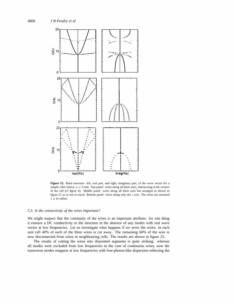
First we ask how important it is that the three sets of wires touch at the corner of the cells.To answer this question we devised the structure shown in figure 21 where the wires arearranged so as not to touch one another.
The result shown in the second panel of figure 22 is interesting: the transverse modesappear almost exactly the same as in the connected geometry, shown for reference in thetop panel, see also figure 6, but the longitudinal mode is very different. The relatively

Low frequency plasmons in thin-wire structures 4805
Figure 20. Band structure: real parts of the wave vector for a simple cubic lattice,a = 5 mm,with cylinders along each axis consisting of ideal metal fibres, assumed 1µ in radius. Thecomponent of the wave vector along thez axis is shown, and the component in the surfaceplane takes a valuekx = π/a, ky = π/a (point E in figure 18). Full lines denote the idealdispersion relationship expected from equation (41) assuming a plasma frequency of 8.3 GHz.
Figure 21. A perspective view of the unit cell for a cubic lattice of non-touching wires. Eachwire bisects a side of the unit cell as shown.
high dispersion of the longitudinal mode means that the structure does not fit our idealmodel, and in particularε depends on bothq andω which gives difficulties when matchingwave functions at the boundary of the material (the additional boundary condition problem).Nevertheless epsilon is undoubtedly negative at low frequencies and this structure meritsfurther investigation.
The most obvious question is whether we need a structure with fibres in all threedirections. The answer is almost obvious: transverse modes travelling along the wires willsurely see nothing of the wires because their electric fields are perpendicular to them, butlongitudinal modes will be strongly affected. Calculations for a single set of wires areshown in the third panel of figure 22.
Note that the transverse modes, the modes which extend down toω = 0, are almostcompletely unaffected by the wires and remain free-photon-like, but the longitudinal modehas atkz = 0 exactly the same frequency, 8.3 GHz, as in both the 3D examples, but itsdispersion withkz is strong, resembling that for the 3D structure of unconnected wires,second panel. The transverse wires, when connected to thez wires, appear to play the roleof confining dispersion of the longitudinal mode withkz.
Although not shown in figure 22, the effect of removing wires parallel to thez axis isto leave the transverse modes unaffected, but to remove the plasma mode completely.
We can summarize the effect of removing sets of wires as follows: those modes whoseelectric fields are parallel to the wires will revert to their free photon format.
4806 J B Pendry et al
Figure 22. Band structure: left, real part, and right, imaginary part, of the wave vector for asimple cubic lattice,a = 5 mm. Top panel: wires along all three axes, intersecting at the cornersof the cell (cf figure 6). Middle panel: wires along all three axes but arranged as shown infigure 21 so as not to touch. Bottom panel: wires along only thez axis. The wires are assumed1 µ in radius.
5.3. Is the connectivity of the wires important?
We might suspect that the continuity of the wires is an important attribute: for one thingit ensures a DC conductivity to the structure in the absence of any modes with real wavevector at low frequencies. Let us investigate what happens if we sever the wires: in eachunit cell 40% of each of the three wires is cut away. The remaining 60% of the wire isnow disconnected from wires in neighbouring cells. The results are shown in figure 23.
The results of cutting the wires into disjointed segments is quite striking: whereasall modes were excluded from low frequencies in the case of continuous wires, now thetransverse modes reappear at low frequencies with free-photon-like dispersion reflecting the

Low frequency plasmons in thin-wire structures 4807
Figure 23. Band structure: left, real part, and right, imaginary part, of the wave vector fora simple cubic lattice,a = 5 mm. Top panel: wires along all three axes, intersecting at thecorners of the cell (cf figure 6); bottom panel: as above but the cylinders are cut into segmentsoccupying 60% of the cell length. The wires are assumed 1µ in radius.
fact that the material is effectively an insulator in the low frequency regime. A longitudinalmode still exists close to the old plasma frequency but can hardly be interpreted as a plasmamode because its controlling influence on the transverse modes has disappeared. In fact theresults look more like those for a system of interacting dipoles [20].
We conclude that continuity of the wires is vital to observing the plasma-like behaviour.Severance of the wires immediately results in reappearance of transverse modes at lowfrequencies and vanishing of the ‘negative epsilon’ property. Other changes to the structurehave less severe consequences. We have experimented with structures into which extralengths of wire have been introduced, for example the structure shown in figure 24.Calculations show that, provided the connectivity of the wires is maintained, the structurecontinues to behave like a plasma, but the plasma frequency is lowered by the extrainductance of the greater length of wire.
6. Conclusions
We have made a thorough investigation of the properties of structures made from 3D arraysof continuous thin wires and shown that the properties of such structures are well describedby a plasma model. The structures are characterized by a plasma frequency below whichall modes decay exponentially, and above which transverse modes propagate like massiveparticles. At the plasma frequency there is a longitudinal mode. These properties wereestablished by analytical modelling (which proved surprisingly accurate), numerical solutionof Maxwell’s equations and finally by experimental investigation.

4808 J B Pendry et al
Figure 24. A connected bent wire structure showing the unit cell on the left, and fourneighbouring cells on the right. The wires are connected at the cell vertices.
The wires had to be continuous and, unless they were thin, the fields penetrated nomore than one layer below the plasma frequency. Using thin wires also reduced the plasmafrequency so that externally incident waves at this frequency had too long a wavelengthto be diffracted. This meant that the system could be accurately described by an effectivedielectric constant of the plasma form.
Having established this principle we now have a playground for creating novel systems.Material with these dielectric properties will couple very strongly to electrical charge andwill be efficient at extracting energy as a form ofCerenkov radiation into the slow travellingmodes near the plasma frequency. Further, the plasma mode can be further tailored by theexternal structure of the composite. For example, the surface of such a composite will behost to a surface plasma mode at
ωs = ωp/√
2. (43)
Although our prime interest in these structures is to develop novel composite materials formicrowave applications, there are other possibilities raised by the structure. The connectionto superconductivity has been alluded to: in particular the negative epsilon property willsurvive down to DC frequencies if the wires are made from superconducting material. Thisraises the intriguing observation that we now can manufacture a composite superconductingmaterial in which the plasma energy, ¯hωp, is of the same order as the pairing energy,1.In conventional superconductors the plasma frequency is much too high to play any directrole in pairing, but could our new composite change this?
The material has an extremely simple internal structure and employs only minuteamounts of metal: structures consisting of parts per million of metal can be active inthe microwave region. This presents us with many opportunities for design.
Acknowledgments
We thank Derek Miller and Dave Clark, of the High Energy Physics group at ImperialCollege, who were responsible for constructing our model negative epsilon structure, alsoLes Hill of GEC–Marconi Materials Technology Ltd who measured the response of themodel. This work has been carried out with the support of the Defence Research Agency,Holton Heath.

Low frequency plasmons in thin-wire structures 4809
References
[1] Sievenpiper D F, Sickmiller M E and Yablonovitch E 1996Phys. Rev. Lett.76 2480[2] Pendry J B, Holden A J, Stewart W J and Youngs I 1996Phys. Rev. Lett.76 4773[3] Yablonovitch E, Gmitter T J and Leung K M 1991 Phys. Rev. Lett.67 2295[4] Yablonovitch E 1993J. Phys.: Condens. Matter5 2443[5] Pendry J B 1996J. Phys.: Condens. Matter8 1085[6] Ritchie R H and Howie A 1981Phil. Mag. A 44 931[7] Echenique P M and Pendry J B 1975J. Phys. C: Solid State Phys.8 2936[8] Ferrell T L and Echenique P M 1985Phys. Rev. Lett.55 1526[9] Echenique P M, Howie A and Wheatley D J 1987Phil. Mag. B 56 335
[10] Howie A and Walsh C A 1991Microsc. Microanal. Microstruct.2 171[11] Ritchie R H 1957Phys. Rev.106 874[12] Stern E A and Ferrell R A 1960 Phys. Rev.120 130[13] Pendry J B and Martın Moreno L 1994Phys. Rev.B 50 5062[14] Pines D and Bohm D 1952Phys. Rev.85 338[15] Bohm D and Pines D 1953Phys. Rev.92 609[16] Anderson P W 1963Phys. Rev.130 439[17] Pendry J B and MacKinnon A 1992Phys. Rev. Lett.69 2772[18] Pendry J B and MacKinnon A 1993J. Mod. Opt.41 209[19] Bell P M, Pendry J B, Martın Moreno L and Ward A J 1995Comput. Phys. Commun.85 306[20] van Coevorden D V, Sprik R, Tip A and Lagendijk A 1996Phys. Rev. Lett.77 2412
![INVITED PAPER PlasmonsinGraphene: …soljacic/graphene_Proceedings_IEEE.pdf · Polarization of graphene and plasmons under strain have been investigated in [54] and [55]. Plasmons](https://img.dokumen.tips/doc/110x75/5ae4b30d7f8b9ae1578b4a90/invited-paper-plasmonsingraphene-soljacicgrapheneproceedingsieeepdfpolarization.jpg)