Embed Size (px)
Citation preview

PAPER • OPEN ACCESS
Unidirectional surface plasmons in nonreciprocalgrapheneTo cite this article: Xiao Lin et al 2013 New J. Phys. 15 113003
View the article online for updates and enhancements.
You may also likeThe Variability of the Black Hole Image inM87 at the Dynamical TimescaleKaushik Satapathy, Dimitrios Psaltis,Feryal Özel et al.
-
The Polarized Image of a Synchrotron-emitting Ring of Gas Orbiting a Black HoleRamesh Narayan, Daniel C. M. Palumbo,Michael D. Johnson et al.
-
Broadband Multi-wavelength Properties ofM87 during the 2017 Event HorizonTelescope CampaignThe EHT MWL Science Working Group, J.C. Algaba, J. Anczarski et al.
-
This content was downloaded from IP address 119.236.186.6 on 02/02/2022 at 17:24

Unidirectional surface plasmonsin nonreciprocal graphene
Xiao Lin1,2,3,4, Yang Xu2,4,6, Baile Zhang3,5, Ran Hao2,Hongsheng Chen1,2,3,4,6 and Erping Li21 State Key Laboratory of Modern Optical Instrumentation, Zhejiang University,Hangzhou 310027, People’s Republic of China2 Department of Information Science and Electronic Engineering, ZhejiangUniversity, Hangzhou 310027, People’s Republic of China3 The Electromagnetics Academy at Zhejiang University, Zhejiang University,Hangzhou 310027, People’s Republic of China4 Cyrus Tang Center for Sensor Materials and Applications, ZhejiangUniversity, Hangzhou 310027, People’s Republic of China5 Division of Physics and Applied Physics, School of Physical andMathematical Sciences, Nanyang Technological University, Singapore 637371,SingaporeE-mail: [email protected] and [email protected]
New Journal of Physics 15 (2013) 113003 (14pp)Received 8 April 2013Published 1 November 2013Online at http://www.njp.org/doi:10.1088/1367-2630/15/11/113003
Abstract. We demonstrate theoretically the existence of unidirectional surfaceplasmons in the nonreciprocal graphene-based gyrotropic interfaces. We showthat a unidirectional frequency range is raised under a static external magneticfield where only one propagating direction is allowed for the surface plasmonsmode. By efficiently controlling the chemical potential of graphene, theunidirectional working frequency can be continuously tunable from THz to near-infrared and even visible. Particularly, the unidirectional frequency bandwidthcan be 1– 2 orders of magnitude larger than that in metal under the same magneticfield, which arises from the superiority of extremely small effective electronmass in graphene. Based on our theoretical analysis, two tunable graphene-based directional devices are proposed, showing the appealing properties ofnonreciprocal graphene in the nonreciprocal optical devices design.
6 Authors to whom any correspondence should be addressed.
Content from this work may be used under the terms of the Creative Commons Attribution 3.0 licence.Any further distribution of this work must maintain attribution to the author(s) and the title of the work, journal
citation and DOI.
New Journal of Physics 15 (2013) 1130031367-2630/13/113003+14$33.00 © IOP Publishing Ltd and Deutsche Physikalische Gesellschaft

2
Surface plasmons originate from the collective excitations of electrons coupled to theelectromagnetic field at the interface between dielectric and metal [1]. Their superb capabilityof confining electromagnetic energy at sub-wavelength scales [1] makes it possible to squeezedown current photonic components to ultracompact nanometer dimensions [1–7]. In particular,surface plasmons have been shown theoretically and experimentally to possess nonreciprocalproperties in the presence of an external static magnetic field [8–15] similar to the chiraledge states of electrons in the quantum Hall effect [16–18]. For example, the heterostructurecomposed of magnetized metal film and two-dimensional (2D) photonic crystal [8, 9] possessesa unidirectional frequency range where only a forward propagating mode is allowed, withneither radiation nor backward modes, being immune from defects [8–10]. However, thepreviously observed nonreciprocity was generally weak and required a very large magneticfield. The design of unidirectional surface plasmons with a large frequency bandwidth under amodest magnetic field, hence, is in great demand for future applications in photonic isolators,diodes and logic circuits.
Graphene [16–18], as a promising one-atom-thick photonic material where the dopedelectrons can be regarded as 2D electron gases (2DEGs), can support surface plasmonswith widely tunable frequencies and reduced losses [19–24]. Recent advances in fabricationhave enabled rapid progress in graphene plasmonics [25–34]. The photon–electron couplingin graphene is remarkably strong compared with that in metals (e.g. silver and gold) and2DEGs in conventional semiconductors [19]. It mainly arises from both the extremely smalleffective electron mass at Fermi energy (i.e. cyclotron effective mass) meff [16–19, 35]and the efficiently tunable electrical gating in graphene [19]. In conventional 2DEGs, thefield induced 2D carrier density ns is limited to ∼1 × 1012 cm−2 to avoid semiconductordielectric breakdown [19]. However, ns in graphene can be tuned by doping or gating fromvery low (1010 cm−2) to very high values (1014 cm−2) [19, 20, 36, 37]. Furthermore, meff
in graphene (meff = 0.02m0 at ns = 1 × 1012 cm−2, m0 is the mass of free electron [19]) isabout two orders of magnitude smaller than that of free electron in metal, and thus theintegrated plasmon oscillator strength is correspondingly much larger [19]. These appealingproperties of graphene have motivated extensive investigations in the emerging research fieldof graphene plasmonic and metamaterial devices [25–34], including optical sensors [38],photodetectors [39, 40], modulators [24, 41–43], waveguides [21, 22], antenna [44], lens[45, 46], Mach–Zehnder interferometers [47], cloaks [48], etc. Recently, significantexperimental progress on unidirectional edge magnetoplasmons in a single graphene sheetwas reported [33]. However, theoretical investigations on unidirectional surface plasmons innonreciprocal graphene have been rarely discussed.
In this paper, we present a theoretical study of nonreciprocal graphene and its applicationsto unidirectional surface plasmons. An externally applied static magnetic field B, which isassumed in the +z direction and perpendicular to the graphene plane (x–y plane), breaks thetime-reversal symmetry in graphene and makes graphene gyrotropic. Two feasible waveguidestructures, air/graphene single interface and air/graphene/dielectric double interfaces, are usedfor demonstration. The unidirectional frequency bandwidth is shown proportional to 1/meff,where meff is dependent on chemical potential µc in graphene. Hence, we show that evenunder a modest magnetic field (|B| = 0.1 T), graphene with small meff is proven capableof making the unidirectional frequency bandwidth very large. Moreover, by controlling µc,the unidirectional working frequency is widely tunable from terahertz (THz) to visible.Based on theoretical analysis, we proposed magnetic-field-controlled directional optical
New Journal of Physics 15 (2013) 113003 (http://www.njp.org/)

3
components, indicating that nonreciprocal graphene can be a good candidate for future photonicdevice applications.
We start by analyzing graphene’s optical properties. The complex optical conductivity ingraphene (G = G intra + G inter, where G intra and G inter are attributed to intra-band and inter-bandtransitions, respectively [49, 50]) can be modeled by the Kubo formula [21, 48–50],
G intra(ω, µc, τ, T ) =ie2kBT
π h̄2(ω + i/τ)
(µc
kBT+ 2 ln(e−µc/kBT + 1)
), (1)
G inter(ω, µc, τ, T ) =ie2(ω + i/τ)
π h̄2
∫∞
0
fd(−E) − fd(E)
(ω + i/τ)2 − 4(E/h̄)2dE, (2)
which relate to chemical potential µc, radian frequency ω, relaxation time τ and temperature T(assuming T = 300 K in this work). E is the energy, e is electron charge, h̄ is reduced Planck’sconstant, kB is Boltzmann’s constant and fd(E) = (e(E−µc)/kBT + 1)−1 is the Fermi–Diracdistribution. Since a DC mobility of µ > 100 000 cm2 V−1 s−1 has been experimentally achievedin high-quality suspended graphene [17, 51] and µ > 60 000 cm2 V−1 s−1 in graphene onhexagonal boron nitride (h-BN) substrate was also reported [52], we can obtain τ > 1.8 ps byusing τ = µcµ/(ev2
F) [22] when setting µc = 0.3 eV, where vF ≈ 0.95 × 10⁶ m s−1 is the Fermivelocity. To model one-atom-thick graphene in macroscopic electromagnetic description, thegraphene can be treated as an ultrathin film with thickness d = 1 nm according to the previouswork [19, 21, 22, 45]. Since the graphene carriers are well localized within one-atom thicklayer (x–y plane), the relative anisotropic permittivity in graphene [45] can be characterizedas diag[εeqεeqεz], where εeq and εz are the components that are parallel and perpendicular tothe graphene plane, respectively [45]. The equivalent complex permittivity εeq parallel to thegraphene plane can be cast into the Drude form [19, 21, 22, 47, 53],
εeq = 1 + iG intra + G inter
ωε0d= εinter + i
G intra
ωε0d= εinter −
ω2p
ω(ω + i/τ), (3)
where εinter = (1 + iG inter/ωε0d) and ε0 is the dielectric permittivity in vacuum. Based onthe macroscopic electromagnetic theory [53], the bulk plasma frequency is defined as ωp =
(Ne2/meffε0)1/2, where N = ns/d is the bulk electron density. For an isolated graphene sheet,
the 2D carrier density ns is determined by the chemical potential µc [49],
ns =2
π h̄2v2F
∫∞
0E[ fd(E) − fd(E + 2µc)] dE . (4)
From equations (1)–(4), both the bulk plasmon frequency ωp and the effective electron massmeff in graphene can be re-written as a function of chemical potential µc,
ωp =
[e2kBT
π h̄2ε0d
(µc
kBT+ 2 ln(e−µc/kBT + 1)
)]1/2
, (5)
meff =
2v2
F
∫∞
0 E[ fd(E) − fd(E + 2µc)] dE
µc + 2kBT ln(e−µc/kBT + 1). (6)
The relations between |ns|1/2, meff, ωp and µc in graphene are shown in figure 1 through
equations (4)–(6). In figure 1, |ns|1/2 and meff increase almost linearly with µc, which is mainly
New Journal of Physics 15 (2013) 113003 (http://www.njp.org/)

4
5
10
|n|1/
2 (cm
-1)
0 0.2 0.4 0.6 0.8 10
200
400
600
800p/2
(TH
z)
c (eV)
0 0.2 0.4 0.6 0.8 10
0.05
0.1
0.15
0.2
mef
f/m0
106
Figure 1. The root of electron density |n|1/2 (green), volume plasma frequency
ωp (blue) and effective electron mass meff (red) as a function of the chemicalpotential µc in graphene. m0 = 0.91 × 10⁻³⁰ kg is the mass of free electron. |n|
1/2
and meff increase almost linearly with µc. The meff of graphene can be 1 or 2orders of magnitude smaller than that of free electron when µc < 0.5 eV.
due to the linear dispersion around the Dirac point in graphene [17–19]. The results shownin figure 1 are consistent with previous works such as [16–19, 35]. For instance, the effectiveelectron mass is massless (i.e. meff = 0) when µc = 0 [17] and meff = 0.02m0 when µc = 0.1 eV(i.e. ns = 1 × 1012 cm−2) [19]. Note that when µc varies in the range of 0–1 eV, meff in grapheneis much smaller than that of free electron in metals.
The design of unidirectional waveguide structures (x–y plane) relies upon the magnetic-field induced nonreciprocity of surface plasmons. As shown in figure 2, we assume that there isno z-variation of the geometry and the fields. In practice, this can be achieved by sandwichinggraphene or graphene with its protecting layers [54–57] (such as 2D h-BN) within two artificialmagnetic conductor structures [53, 58–62], which is a synthesized perfect magnetic conductor(PMC) acting as a confining edge or waveguide similar to that in [9], where the structurecan be regarded as equivalent to infinitely periodically stacked graphene with its protectinglayers along the z direction [8, 41, 54–57, 63–66]. With the help of PMC boundary conditionand based on the macroscopic electromagnetic theory, the three-dimensional (3D) waveguidestructure can then approximately be dealt with as a 2D model. The protecting layer likeh-BN is used to support the graphene and to keep the properties of the graphene, e.g. the smalleffective electron mass and the high electron mobility, when stacking the graphene along thez direction. The stacking periodicity in the paper is assumed to be 1 nm, which is larger thanthat of graphite (0.335 nm). So the interlayer interactions between the graphene sheets in ourpaper can be ignored. It is therefore different from the bulk material of graphite which has layerinteractions but is rather equivalent to a 3D graphene. Meanwhile, since the stacking period ismuch smaller than a wavelength, it could be considered as a homogeneous material. Therefore,our assumption that there is no z-variation of the geometry and the fields is reasonable. For thesake of simplicity, we neglect the protecting layers’ impact and use graphene’s optical parameterto study the 2D model [34]. In the presence of a static magnetic field B along the +z direction,
New Journal of Physics 15 (2013) 113003 (http://www.njp.org/)

5
-4 -2 0 2 4k
x/k
SP
-3 -1-2 0 1 2 390
95
100
105
110
kx/k
SP
(b)
w graphene
air (ε1=1)
air (ε2=1)
(c)
B
graphene
air (ε1=1)
(a)
x
y
z
w graphene
air (ε1=1)
dielectric (ε2=2)
(e)
-4 -2 0 2 4k
x/k
SP
)f()d( ωSPL
ωSPR
surface
plasmonsB B
B=0
B=-10T B=-10 T B=-10T
ωSPL
ωSPR
+ + +
Figure 2. Dispersion relations of surface plasmons propagating along threedifferent graphene based interfaces: (a), (b) air/graphene interface; (c), (d)air/graphene/air interfaces; (e), (f) air/graphene/dielectric interfaces. The top (a),(c), (e) show the corresponding schematic structures. The horizontal axis isthe wave propagation vector normalized by kSP = ωSP(µ0ε0)
1/2. In (c) and (e),graphene has a finite width of w = 0.3 µm. The regions of ωSPR < ω < ωSPL
in (b) and (f) indicate the unidirectional frequency range. B = +10 T and µc =
0.3 eV are used in order to obtain a large unidirectional frequency bandwidth forclear observation.
graphene is gyrotropic and its relative anisotropic permittivity can be described by a tensor [53]:
¯̄ε =
εd iεg 0−iεg εd 0
0 0 εz
, (7)
where εd = εinter − ω2p/(ω
2− ω2
B), εg = −ω2pωB/(ω3
− ωω2B)) and ωB = eB/meff is the cyclotron
frequency. It should be noted that the linear dispersion relation in graphene band structurearound the Dirac point can be quantized as a result of the external magnetic field dueto Landau quantization [16–18]. Therefore, the Drude model expression for the graphenepermittivity tensor in equation (7) has a validity range when an external magnetic field is applied[67, 68]. As reported in [67], as long as the following condition, µc � L , where L =
(2h̄eBv2F)
1/2 is the Landau energy scale, is satisfied, the graphene permittivity tensorcharacterized in our paper is valid. From our calculation, we find that when |B|6 0.1 T (thisrange of B is what we used throughout the paper except figures 2 and 3 for the purpose ofclear observation of the unidirectional bandwidth), the Landau energy scale L is smaller than0.0115 eV, and therefore the condition µc � L can be satisfied. In addition, according to [67],using a larger µc and/or a smaller B can further help to weaken the Landau quantizationinfluence. Therefore, the Landau quantization perturbation will not qualitatively alter our main
New Journal of Physics 15 (2013) 113003 (http://www.njp.org/)

6
Figure 3. Hz field distribution of surface waves excited by a point sourcein four different cases: (a) air/graphene interface without loss (εd = −1.1196,εg = 0.4059), (b) air/graphene interface with loss (εd = −1.1196 + 0.0154i,εg = 0.4059–0.0007i), (c) air/graphene/air symmetric double interfaces and (d)air/graphene/dielectric (ε = 2) asymmetric double interfaces. Graphene regionis marked in yellow. The parameters are: µc = 0.3 eV, B = +10 T. The workingfrequency f0 = 105 THz is both within the unidirectional frequency range ofair/graphene interface (103.3 to 108.0 THz) and that of air/graphene/dielectricinterfaces (104 to 108.0 THz).
conclusion below. For simplicity, we do not consider the Landau quantization perturbation inthis paper. The z-component permittivity εz will not change when graphene is under a z-directionexternal magnetic field. When neglecting the loss in graphene characterized by the relaxationtime τ , the single gyrotropic interface between graphene and dielectric (with ε1) in figure 2(a)supports surface plasmons with the following dispersion relation:
(ε2d − ε2
g)
√k2
x − ω2µ0ε0ε1 + εd
√k2
x − ω2µ0ε0(ε2d − ε2
g)/εd + εgkx = 0, (8)
where kx is the component of wave vector along propagation direction (x direction) and µ0 isthe permeability in vacuum. The dispersion relation is then plotted in figure 2(b) by assumingµc = 0.3 eV and B = +10 T. Note that a larger external magnetic field like 10 T may influencethe graphene band structures due to Landau quantization [16–18]. Here it is used only to obtaina large unidirectional frequency bandwidth for clear observation in figure 2. From figure 2(b),the linear term of kx in equation (8) breaks the left–right symmetry of the dispersion relation. Inthe limit of |ωB| � ωp, the frequencies of the left and right propagating modes approach theirupper limits of ωSPL = ωSP + |ωB|/2 and ωSPR = ωSP − |ωB|/2 at kx → ∓∞, respectively, where
New Journal of Physics 15 (2013) 113003 (http://www.njp.org/)

7
ωSP = ωp/(ε1 + εinter)1/2. Within the unidirectional frequency range ωSPR < ω < ωSPL, surface
plasmons can only propagate in one direction. We simulate the performance of unidirectionalsurface plasmons by using the finite element method (COMSOL Multiphysics). A point sourceat the interface is used to excite the field. Figure 3(a) shows the propagation of the surfaceplasmons in lossless graphene while figure 3(b) shows the results when a loss characterized by arelaxation time τ = 0.9 ps is included. One can see that both cases can support the unidirectionalsurface plasmons mode.
Now we extend our study to finite-width graphene as often used in practice. We considerthe structure of dielectric (with ε1)/graphene (with ¯̄ε)/dielectric (with ε2) as an example. Whenthe graphene strip has a finite width comparable with the skin depth (dskin = 0.25 µm), surfaceplasmons in the gyrotropic interfaces can couple efficiently with each other. The dispersionrelation of surface plasmons in this structure is derived as follows:
e−2kgy I w =(κdkgy I − κgkx) + k1y I
ε1
(κdkgy I + κgkx) −k1y I
ε1
(κdkgy I + κgkx) + k2y I
ε2
(κdkgy I − κgkx) −k2y I
ε2
, (9)
where κd = εd/(ε2d− ε2
g), κg = −εg/(ε2d− ε2
g), kgy I =
√k2
x − ω2µ0ε0(ε2d − ε2
g)/εd , k1y I =√k2
x − ω2µ0ε0ε1 and k2y I =√
k2x − ω2µ0ε0ε2. When w = 0.3 µm (slightly larger than the skin
depth dskin), µc = 0.3 eV, B = +10 T, the dispersion relations for the air/graphene/air structure(ε1 = ε2, as shown in figure 2(c)) and that for the air/graphene/dielectric (ε1 6= ε2, as shownin figure 2(e)) are plotted in figures 2(d) and (f), respectively. When the double interfaces aresymmetric (ε1 = ε2), equation (9) becomes
e−2kgy I w =
(κdkgy I + k1y I
ε1
)2− (κgkx)
2(κdkgy I −
k1y I
ε1
)2− (κgkx)2
(10)
without the linear term of kx . In this case, the left–right symmetry of the dispersion relation ispreserved and the unidirectional frequency bandwidth is zero as shown in figure 2(d), indicatingthat the symmetric double interfaces cannot support unidirectional surface plasmons. Whenω < ωSP + |ωB|/2, the numerical simulation in figure 3(c) shows that surface plasmons alongthe symmetric double interfaces can propagate in both directions. In contrast, equation (9) inasymmetric double interfaces (ε1 6= ε2) always has a linear term of kx , similar to that in singlegyrotropic interface, indicating that it can support the propagation of unidirectional surfaceplasmon mode. The result shown in figure 2(f) clearly indicates that the left–right symmetry ofthe dispersion relation is broken. In the limit of |ωB| � ωp, the asymmetric double interfaceshave a unidirectional frequency bandwidth ωSPL − ωSPR ≈ 0.85|ωB|, which is a bit smaller thanthat in air/graphene single interface. When the working frequency is within the unidirectionalfrequency range, the numerical simulation in figure 3(d) shows that the asymmetric interfacescan support unidirectional surface plasmons. Therefore, from the comparison of the resultsshown in figures 3(c) and (d), one can see that the unidirectional surface plasmons can onlybe excited in asymmetric double interfaces.
From the above theoretical analysis, we can conclude that graphene shows the followingsuperiorities in designing unidirectional surface plasmons compared to metal:
Firstly, the working frequency can be widely tuned by the chemical potential µc. Since theworking frequency range (ωSP − |ωB|/2 < ω < ωSP + |ωB|/2) of air/graphene interface relates
New Journal of Physics 15 (2013) 113003 (http://www.njp.org/)

8
Figure 4. Unidirectional frequency bandwidth ((ωPSL − ωPSR)/2π , red line)and lowest unidirectional working frequency (ωPSR/2π , blue line) of surfaceplasmons at the air/graphene interface under a static magnetic field (B = +0.1 T)as a function of the chemical potential µc in graphene. As µc increases to 1 eV,the unidirectional working frequency changes continuously from several THz toseveral hundred THz. Compared with that in air/metal interface (|eB/2πm0| =
0.0028 THz, gray dashed arrow), the unidirectional frequency bandwidth ofair/graphene interface can be 1–2 orders of magnitude larger under the samemagnetic field.
to ωSP, ωSP = ωp/(ε1 + εinter)1/2, and ωp increases with µc (as shown in figure 1), the working
frequency can be tuned through efficiently controlling µc in graphene. When a modest magneticfield B = +0.1 T is applied in air/graphene interface, the lowest working frequency ωSPR =
ωSP − |ωB|/2 as a function of µc is shown in figure 4. One can see that when µc increasesfrom 0.1 eV to 1.0 eV, ωSPR increases almost linearly from several THz to several hundred THz(near infrared). Our calculated results also show (not shown in figure 4) that when µc > 1.5 eV,ωSPR is larger than 400 THz (visible light spectrum). Note that the electron doping densitycan reach 4 × 1014 cm−2, which corresponds to µc = 2.2 eV and has already been achieved inprevious experiments [37]. Hence, the working frequency of the graphene-based unidirectionalsurface plasmons can span a wide frequency range from several THz to visible light spectrumby controlling the chemical potential.
Secondly, a unidirectional frequency range much larger than that in metals can be achievedin graphene. This is because in the limit of |ωB| � ωp, the unidirectional frequency bandwidth|ωB| = e|B|/meff is proportional to |B| and inversely proportional to meff, and it is well knownthat meff in graphene, which decreases linearly as µc decreases, can be extremely smaller thanthat in metal, as shown in figure 1. When B = +0.1 T and µc = 0.1 eV, the unidirectionalfrequency bandwidth is 0.12 THz in air/graphene interface, which is about 43 times widerthan that in air/metal interface, i.e. 0.0028 THz. In general, from figure 4, one can see that theunidirectional frequency bandwidth, (ωPSL − ωPSR)/2π , in air/graphene interface can be 1–2orders of magnitude larger than that in air/metal interface under the same magnetic field.
The unidirectional surface plasmons can be used to design reconfigurable directionaloptical components. As a concrete example, a Y-shaped directional surface plasmon waveguideis designed as shown in figure 5. The Y-shaped waveguide is composed of two parts. The left part
New Journal of Physics 15 (2013) 113003 (http://www.njp.org/)

9
Figure 5. Hz field distribution of the Y-shaped graphene-based directionalwaveguide controlled by an external static magnetic field: (a) B = 0, (b) B =
+0.1 T, (c) B = –0.1 T. Graphene region is marked in yellow. The parametersare: µc = 0.1 eV, f0 = 42.7 THz, w = 0.8 µm, r = 5 µm. The wave is incidentfrom port 1 and flows to ports 2 and/or port 3.
of the Y-shaped waveguide (port 1) is the air/graphene/air interfaces, and the right part consistsof two branches (port 2 and port 3), each composed of an air/graphene interface. The graphenewidth in the left part is w = 0.8 µm and the radius of the interface in the right part is r = 5 µm.The chemical potential in graphene is µc = 0.1 eV. The working frequency is f0 = 42.7 THz.The surface wave is incident from the left (port 1), propagates along the air/graphene/airinterfaces, and outputs to the right down branch (port 2) and/or the right up branch (port 3).The propagating behavior of surface plasmons in the right part can be controlled by the externalmagnetic field B. Three cases with different external magnetic fields are studied. In the first case,B = 0 (εd = −1.0196, εg = 0), the two separate air/graphene interfaces at the output branchesare reciprocal and support surface plasmons in both directions. The surface waves input fromport 1 therefore couple with port 2 and port 3 equally, as shown in figure 5(a). It behaves similarto a power divider. In the second case, B = +0.1 T (εd = −1.0198, εg = 0.052); unidirectionalsurface plasmons mode will be raised in this case. The working frequency f0 = 42.7 THzis right within the unidirectional frequency range of air/graphene interface (from 42.6628to 42.7823 THz). The skin depth of unidirectional surface plasmons along the air/grapheneinterface is dskin = 0.3 µm in the graphene region. Therefore, the air/graphene interface onlysupports the right-direction surface plasmons in port 2 and the left-direction surface plasmonsin port 3. Figure 5(b) shows the simulation results, from which one can see that the powerfrom port 1 couples with port 2 completely. In the third case, B = −0.1 T (εd = −1.0198,εg = −0.052). Because of that, the direction of external magnetic field is reversed; the directionsof unidirectional surface modes that port 2 and port 3 can support are reversed in this case.Figure 5(c) shows that the surface waves input from port 1 completely couple with port 3. Thesimulations, therefore, suggest a novel directional surface plasmon waveguide tuned by externalmagnetic field.
With the tunability of the operating frequency by the chemical potential µc, the graphene-based unidirectional surface plasmons can be used to realize more advanced photonic devices.As an example, we designed a tunable four-port surface plasmon waveguide coupler, which cancouple the waves from one port with any of the other three ports freely. The four-port coupler
New Journal of Physics 15 (2013) 113003 (http://www.njp.org/)

10
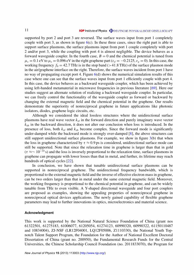
Figure 6. Hz field distribution of four-port graphene-based surface plasmoncoupler. The parameters are: µc = 0.1 eV, f0 = 42.7 THz, w = 0.8 µm and r =
5 µm. Wave is incident from port 1 and flows to output ports 2, 3 and 4. In theleft graphene part, magnetic field is B = +0.1 T. In the right part, magnetic fieldis (a) B = 0, (b) B = +0.1 T, (c) B = –0.1 T and (d) B = 0, respectively. In theright graphene part in (d), the chemical potential is tuned to µc = 0.096 eV toobtain the backward coupling. The graphene region is marked in yellow.
is composed of three parts. The left and right parts are four branches (port 1, port 2, port 3and port 4), each composed of an air/graphene interface, as shown in figure 6. The middlepart, which can be considered as the couple region, is the reciprocal air/graphene/air interfaces.The parameters used are the same as in figure 5: w = 0.8 µm, r = 5 µm, µc = 0.1 eV andf0 = 42.7 THz. In the designed waveguide coupler, the four ports can couple freely by tuningthe magnetic field and/or chemical potential in the left and right graphene parts separately.In figure 6, we demonstrate how the surface wave that is incident from port 1 can be freelycoupled to any of the other three ports by properly selecting the B and µc. The left graphenepart is set with B = +0.1 T (εd = −1.0198, εg = 0.052), and thus the nonreciprocal air/grapheneinterface can only support right-direction surface plasmons in port 1 and left-direction surfaceplasmons in port 4. In the right graphene part, the following four cases with different externalmagnetic fields are studied. In the first case, B = 0 (εd = −1.0196, εg = 0), the two separateair/graphene interfaces on the right are reciprocal. The surface waves input from port 1 aretherefore coupled with port 2 and port 3 equally, as shown in figure 6(a). In the second case,B = +0.1 T (εd = −1.0198, εg = 0.052), the air/graphene interface at port 2 only supports right-direction surface plasmon mode and at port 3 only supports left-direction surface plasmon mode.Hence, the power from port 1 couples with port 2 completely, as shown in figure 6(b). In thethird case, B = −0.1 T (εd = −1.0198, εg = −0.052); because of the reverse of externalmagnetic field direction in the second case, the directions of unidirectional surface modes
New Journal of Physics 15 (2013) 113003 (http://www.njp.org/)
11
supported by port 2 and port 3 are reversed. The surface waves input from port 1 completelycouple with port 3, as shown in figure 6(c). In these three cases, since the right part is able tosupport surface plasmons, the surface plasmons input from port 1 couple completely with port2 and/or port 3, while the coupling with port 4 is almost negligible. The device behaves as aforward waveguide coupler. In the fourth case, B = 0 and the chemical potential is tuned fromµc = 0.1 eV to µc = 0.096 eV in the right graphene part (εd = −0.2125, εg = 0). In this case, theworking frequency f0 = 42.7 THz is in the stop band (>41.8 THz) of the surface plasmon modein the air/graphene interface on the right. Therefore, the surface waves incident from port 1 haveno way of propagating except port 4. Figure 6(d) shows the numerical simulation results of thiscase where one can see that the surface waves input from port 1 efficiently couple with port 4.In this case, the device behaves as a backward waveguide coupler, which has been achieved byusing left-handed metamaterial in microwave frequencies in previous literature [69]. Here ourstudies suggest an alternate solution of realizing a backward waveguide coupler. In particular,we can freely control the functionality of the waveguide coupler as forward or backward bychanging the external magnetic field and the chemical potential in the graphene. Our resultsdemonstrate the superiority of nonreciprocal graphene in future applications like photonicisolators, diodes, graphene logic circuits, etc.
Although we considered the ideal lossless structures where the unidirectional surfaceplasmons have real wave vector kxf in the forward direction and purely imaginary wave vectorkxb in the backward direction, it does not alter our conclusion when loss is introduced. In thepresence of loss, both kxf and kxb become complex. Since the forward mode is significantlyunder-damped while the backward mode is strongly over-damped [8], the above structures canstill support unidirectional surface plasmons. For example, we show in figure 3(b) that whenthe loss in graphene characterized by τ ≈ 0.9 ps is considered, unidirectional surface mode canstill be supported. Note that since the relaxation time in graphene is larger than that in gold(τ ≈∼ 10−14 s) and the loss is inversely proportional to the relaxation time, surface plasmons ingraphene can propagate with lower losses than that in metal, and further, its lifetime may reachhundreds of optical cycles [22].
In conclusion, we have shown that tunable unidirectional surface plasmons can besupported in nonreciprocal graphene. The unidirectional frequency bandwidth, which isproportional to the external magnetic field and the inverse of effective electron mass in graphene,can be two orders larger than that in metal under the same external magnetic field. Moreover,the working frequency is proportional to the chemical potential in graphene, and can be widelytunable from THz to even visible. A Y-shaped directional waveguide and four port couplersare proposed as examples, showing the appealing properties of nonreciprocal graphene innonreciprocal optical devices applications. The newly gained capability of flexible grapheneparameters may lead to further innovations in optics, microelectronics and material science.
Acknowledgment
This work is supported by the National Natural Science Foundation of China (grant nos61322501, 61275183, 61006077, 61205054, 61274123, 60990320, 60990322, 61150110487and 10834004), ZJ-NSF (LR12F04001, LQ12F05006, Z1110330), the National Youth Top-notch Talent Support Program, the Foundation for the Author of National Excellent DoctoralDissertation of China (grant no. 200950), the Fundamental Research Funds for the CentralUniversities, the Chinese Scholarship Council Foundation (no. 2011833070), the Program for
New Journal of Physics 15 (2013) 113003 (http://www.njp.org/)

12
New Century Excellent Talents (NCET-12-0489) in University, the K P Chao’s High TechnologyDevelopment Foundation, the National Specialized Research Fund for the Doctoral Programof Higher Education (SRFDP with grant no. 20100101120045) and Innovation platformfor Micro/Nano Device and System Integration at Zhejiang University. BZ acknowledgesfunding support from Nanyang Technological University under grant nos M4080806.110 andM4081153.110 and Singapore Ministry of Education under grant nos M4011039.110 andMOE2011-T3-1-005.
References
[1] Maier S A 2007 Plasmonics: Fundamentals and Applications (Berlin: Springer)[2] Gramotnev D K and Bozhevolny S I 2010 Plasmonics beyond the diffraction limit Nature Photon. 4 83–91[3] Barnes W L, Dereux A and Ebbesen T W 2003 Surface plasmon subwavelength optics Nature 424 824–30[4] Berini P and Leon I D 2011 Surface plasmon-polariton amplifiers and lasers Nature Photon. 6 16–24[5] Temnov V V et al 2010 Active magneto-plasmonics in hybrid metal ferromagnet structures Nature Photon.
4 107–11[6] Poo Y et al 2011 Experimental realization of self-guiding unidirectional rlectromagnetic edge states Phys.
Rev. Lett. 106 093903[7] Yu Z and Fan S 2009 Complete optical isolation created by indirect interband photonic transitions Nature
Photon. 3 91–4[8] Yu Z et al 2008 One-way electromagnetic waveguide formed at the interface between a plasmonic metal
under a static magnetic field and a photonic crystal Phys. Rev. Lett. 100 023902[9] Wang Z et al 2009 Observation of unidirectional backscattering-immune topological electromagnetic states
Nature 461 772–5[10] Haldane F D M and Raghu S 2008 Possible realization of directional optical waveguides in photonic crystals
with broken time-reversal symmetry Phys. Rev. Lett. 100 013904[11] Wang Z et al 2008 Reflection-free one-way edge modes in a gyromagnetic photonic crystal Phys. Rev. Lett.
100 013905[12] Khanikaev A B et al 2010 One-way extraordinary optical transmission and nonreciprocal spoof plasmons
Phys. Rev. Lett. 105 126804[13] Yablonovitch E 2009 One-way road for light Nature 461 744–5[14] Dı́az J B G et al 2007 Surface magnetoplasmon nonreciprocity effects in noble metal/ferromagnetic
heterostructures Phys. Rev. B 76 153402[15] Zhu H and Jiang C 2010 Broadband unidirectional electromagnetic mode at interface of anti-parallel
magnetized media Opt. Express 18 6914–21[16] Zhang Y et al 2005 Experimental observation of the quantum Hall effect and Berry’s phase in graphene
Nature 438 201–4[17] Novoselov K S et al 2005 Two-dimensional gas of massless Dirac fermions in graphene Nature 438 197–200[18] Neto A H C et al 2009 The electronic properties of graphene Rev. Mod. Phys. 81 109–62[19] Ju L et al 2011 Graphene plasmonics for tunable terahertz metamaterials Nature Nanotechnol. 6 630–4[20] Rana F 2011 Graphene optoelectronics: plasmons get tuned up Nature Nanotechnol. 6 611–2[21] Vakil A and Engheta N 2011 Transformation optics using graphene Science 332 1291–4[22] Christensen J et al 2012 Graphene plasmon waveguiding and hybridization in individual and paired
nanoribbons ACS Nano 6 431–40[23] Koppens F H L, Chang D E and Abajo F J G 2011 Graphene plasmonics: a platform for strong light–matter
interactions Nano Lett. 11 3370–7[24] Liu M et al 2011 A graphene-based broadband optical modulator Nature 474 64–7[25] Fei Z et al 2012 Gate-tuning of graphene plasmons revealed by infrared nano-imaging Nature 487 82–5[26] Chen J et al 2012 Optical nano-imaging of gate-tunable graphene plasmons Nature 487 77–81
New Journal of Physics 15 (2013) 113003 (http://www.njp.org/)

13
[27] Thongrattanasiri S, Koppens F H L and Abajo F J G 2012 Complete optical absorption in periodicallypatterned graphene Phys. Rev. Lett. 108 047401
[28] Papasimakis N et al 2010 Graphene in a photonic metamaterial Opt. Express 18 8353–9[29] Chen C F et al 2011 Controlling inelastic light scattering quantum pathways in graphene Nature 471 617–20[30] Jablan M, Buljan H and Soljacic M 2009 Plasmonics in graphene at infrared frequencies Phys. Rev. B
80 245435[31] Yan H et al 2012 Infrared spectroscopy of tunable Dirac terahertz magneto plasmons in graphene Nano Lett.
12 3766–71[32] Crassee I et al 2012 Intrinsic terahertz plasmons and magnetoplasmons in large scale monolayer graphene
Nano Lett. 12 2470–4[33] Petkovic I et al 2013 Carrier drift velocity and edge magnetoplasmons in graphene Phys. Rew. Lett.
110 016801[34] Lin X et al 2013 Ab initio optical study of graphene on hexagonal boron nitride and fluorographene substrates
J. Mater. Chem. C 1 1618–27[35] Ariel V and Natan A 2012 Electron effective mass in graphene arXiv:1206.6100[36] Das A et al 2008 Monitoring dopants by Raman scattering in an electrochemically top-gated graphene
transistor Nature Nanotechnol. 3 210–5[37] Efetov D K and Kim P 2010 Controlling electron–phonon interactions in graphene at ultrahigh carrier
densities Phys. Rev. Lett. 105 256805[38] Schedin F et al 2010 Surface-enhanced Raman spectroscopy of graphene ACS nano 4 5617–26[39] Echtermeyer T et al 2011 Strong plasmonic enhancement of photovoltage in graphene Nature Commun. 2 458[40] Bao Q and Loh K P 2012 Graphene photonics, plasmonics and broadband optoelectronic devices ACS Nano
6 3677–94[41] Rodriguez B S et al 2012 Broadband graphene terahertz modulators enabled by intraband transitions Nature
Commun. 3 780[42] Lee S H et al 2012 Switching terahertz waves with gate-controlled active graphene metamaterials Nature
Mater. 11 936–41[43] Weis P et al 2012 Spectrally wide-band terahertz wave modulator based on optically tuned graphene ACS
Nano 6 9118–24[44] Fang Z et al 2012 Graphene-antenna sandwich photodetector Nano Lett. 12 3808–13[45] Wang J et al 2012 Ultraviolet dielectric hyperlens with layered graphene and boron nitride J. Mater. Chem.
22 15863[46] Li P and Taubner T 2012 Broadband subwavelength imaging using a tunable graphene lens ACS Nano
6 10107–14[47] Wang B et al 2012 Optical coupling of surface plasmons between graphene sheets Appl. Phys. Lett.
100 131111[48] Chen P Y and Alu A 2011 Atomically thin surface cloak using graphene monolayers ACS Nano 5 5855–63[49] Hanson G W 2008 Dyadic Green’s functions and guided surface waves for a surface conductivity model of
graphene J. Appl. Phys. 103 064302[50] Gusynin V P, Sharapov S G and Carbotte J P 2007 Magneto-optical conductivity in graphene J. Phys.:
Condens. Matter 19 026222[51] Bolotin K I et al 2008 Ultrahigh electron mobility in suspended graphene Solid State Commun. 146 351–5[52] Dean C R et al 2010 Boron nitride substrates for high-quality graphene electronics Nature Nanotechnol.
5 722–6[53] Kong J A 2008 Electromagnetic Wave Theory (Cambridge, MA: EMW Publishing)[54] Ponomarenko L A et al 2011 Tunable metal-insulator transition in double-layer graphene heterostructures
Nature Phys. 7 958–61[55] Britnell L et al 2012 Field-effect tunneling transistor based on vertical graphene heterostructures Science
335 947–50
New Journal of Physics 15 (2013) 113003 (http://www.njp.org/)

14
[56] Gorbachev R V et al 2012 Strong Coulomb drag and broken symmetry in double layer graphene Nature Phys.8 896–901
[57] Mayorov A S et al 2011 Micrometer-scale ballistic transport in encapsulated graphene at room temperatureNano Lett. 11 2396–9
[58] Kim Y, Yang F and Elsherbeni A Z 2007 Compact artificial magnetic conductor designs using planar squarespiral geometries Prog. Electromagnetics Res. 77 43–54
[59] Kern D J et al 2005 The design synthesis of multiband artificial magnetic conductors using high impedancefrequency selective surfaces IEEE Trans. Antennas Propag. 53 8–17
[60] Cos M E et al 2010 Novel SHF-band uniplanar artificial magnetic conductor IEEE Antennas Wireless Propag.Lett. 9 44–7
[61] Zhang Y et al 2003 Planar artificial magnetic conductors and patch antennas IEEE Trans. Antennas Propag.51 2704–12
[62] Sievenpiper D et al 1999 High-impedance electromagnetic surfaces with a forbidden frequency band IEEETrans. Microwave Theory Tech. 47 2059–74
[63] Sakai Y, Koretsune T and Saito S 2011 Electronic structure and stability of layered superlattice composed ofgraphene and boron nitride monolayer Phys. Rev. B 83 205434
[64] Kaloni T P, Cheng Y C and Schwingenschlogl U 2012 Electronic structure of superlattices of graphene andhexagonal boron nitride J. Mater. Chem. 22 919
[65] Xu Y et al 2012 Ab initio study of energy band modulation in graphene-based two dimensional layeredsuperlattices J. Mater. Chem. 22 23821–9
[66] Haigh S J et al 2012 Cross-sectional imaging of individual layers and buried interfaces of graphene-basedheterostructures and superlattices Nature Mater. 11 764–7
[67] Sounas D L and Caloz C 2012 Gyrotropy and nonreciprocity of graphene for microwave applications IEEETrans. Microwave Theory Tech. 60 901–14
[68] Kubo R 1957 Statistical-mechanical theory of irreversible processes. I. general theory and simple applicationsto magnetic and conduction problems J. Phys. Soc. Japan 12 570–86
[69] Yuan Y et al 2006 Backward coupling waveguide coupler using left-handed material Appl. Phys. Lett.88 211903
New Journal of Physics 15 (2013) 113003 (http://www.njp.org/)