Embed Size (px)
Citation preview

1 1
Low ESH-impact Gate Stack Fabrication by Selective Surface Chemistry
Shawn Miller and Anthony Muscat Department of Chemical and Environmental Engineering
University of Arizona, Tucson, AZ 85721
Industrial partners: SFAZ ASM
ERC Teleconference Feb, 9th 2012 Tucson, AZ
(Task Number: 425.026)

2 2
Overall Objectives
• Simplify multistep subtractive processing used in microelectronic device manufacturing
– Develop new additive processes that can be integrated into current devices flows
• Focus on high-k gate stack testbed – Fabricate low defect high-k/semiconductor interfaces
3 3
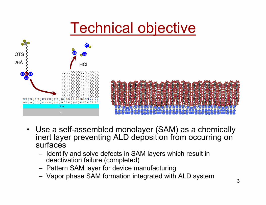
Technical objective
• Use a self-assembled monolayer (SAM) as a chemically inert layer preventing ALD deposition from occurring on surfaces – Identify and solve defects in SAM layers which result in
deactivation failure (completed) – Pattern SAM layer for device manufacturing – Vapor phase SAM formation integrated with ALD system
OTS
26Å HCl
4 4
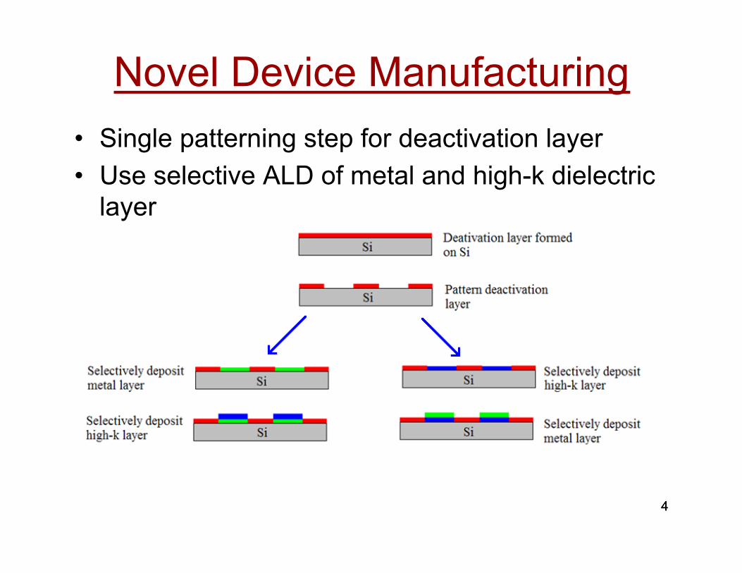
Novel Device Manufacturing • Single patterning step for deactivation layer • Use selective ALD of metal and high-k dielectric
layer

5 5
ESH Metrics and Impact: Cost Reduction
• Safety of SAM solution – Chlorosilanes dissolved in toluene
• Chlorosilanes reacts with water, air sensitive, and combustible – OTS (octadecyltrichlorosilane) – TMCS (trimethylchlorosilane)
• Batch processing must be done in vented environment with controlled humidity and no spark or open flame
• Vapor process could eliminate solvent – Carbon and HCl are only byproducts of the surface reaction
OTS TMCS

6
• Additional benefits of hydrophobic surface – SAM coating prevents aqueous solutions from interacting with surfaces
• Coating metal parts or work surfaces which are exposed to water-based solution reduces the need for cleaning such tools/equipment
• Coat ALD reactor walls with SAM to extend up-time, reduce cleaning, and improve throughput
ESH Metrics and Impact: Cost Reduction
6

7 7
SAM Defects
• (A) Poor alignment at island boundaries block surface sites (poor uniformity)
• (B,C) Gaps in SAM too small for primary SAM molecule • (D) Water absorbed/adsorbed in SAM layer
– Either during SAM formation or during ALD process • (E) Polymerized SAM molecules on surface
– Block surface sites – Excess polymer increases thickness and water contact angle – Could generate particles
26Å
OTS TMCS

8 8
Defect monitoring using TiCl4 pulses Ti Saturation Level
0
0.05
0.1
0.15
0.2
0.25
0.3
0.35
0 100 200 300
Number of TiCl4 Pulses
Ti T
hick
ness
(Å)
2hr OTS, piranha
48hr OTS, piranha
48hr OTS, nitric
24hr OTS, Chloroform, 24hr OTS, nitric
24hr OTS, SC1, 24hr OTS, nitric
SiO2-OH
• Defect level in SC1 re-hydroxylated samples was below XPS limit for up to 250 seconds of TiCl4 exposure
9
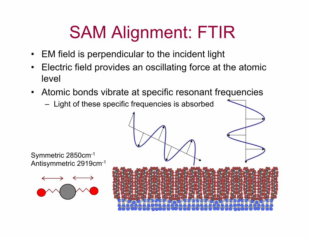
SAM Alignment: FTIR • EM field is perpendicular to the incident light • Electric field provides an oscillating force at the atomic
level • Atomic bonds vibrate at specific resonant frequencies
– Light of these specific frequencies is absorbed
Symmetric 2850cm-1
Antisymmetric 2919cm-1

10
Analysis of CH2 peaks Nitric acid/piranha
• At 2h the OTS layer formed on piranha and nitric are similar for both normal and Brewster incidence
• At 24h the CH2 peak areas from the piranha prepared sample were double the peak area of nitric etched samples for normal incidence and nearly five times the area for the Brewster angle
– This suggests that after 24h the piranha prepped sample has far more polymerization and misaligned molecules
• After extraction or SC1 re-hydroxylation the samples are similar again
2h 24h 24h ext 24h sc1 24h ext 24h 24h sc1
24h 0.8453 0.5169 0.7403 0.6584 0.7953 0.8700 0.9553 0.5501 0.8403 0.7036 0.8836 1.0046
0.6389 0.2193 0.9715 0.8973 1.1104 1.0415 0.8632 0.2819 1.0876 0.9818 0.9906 1.1663
NORMAL incidence Symmetric 2850cm-1
Antisymmetric 2919cm-1
BREWSTER incidence Symmetric 2850cm-1
Antisymmetric 2919cm-1

11
Analysis of CH2 peaks Brewster angle/Normal
Incidence
2850cm-1
2919cm-1
10min 2h 24h 24h ext 24h sc1 24h ext 24h 24h sc1
24h
nitric 1.1662 0.2919 0.5202 3.4516 3.1325 4.3249 3.2451
piranha 1.4577 0.3555 1.2263 2.6300 2.2984 2.6947 2.7108
nitric 1.5863 0.3555 0.6270 3.3091 3.1431 3.8493 3.3328
piranha 1.7846 0.3934 1.2236 2.5567 2.2524 2.6113 2.8707
30
25
20
15
10
5
0
x10-3
30002950290028502800Wave Number
Brewster IncidenceNormal Incidence
24h
2h

12 12
Selective high-k deposition
• SAM surfaces exposed to UV in air for 2.5 h through a simple mask
• Removal of SAM occurred only in UV/air exposed areas
• Surface was hydrophilic in UV/air exposed areas and hydrophobic on remaining OTS areas
110° 5 - 25° 110 ° Water contact angle

13 13
Direct SAM patterning • Selectively deposited 30Å of TiO2 only in open
areas of OTS coated Si surface • Pattern formed without photoresist
40
20
0
x103
1000 800 600 400 200 0Binding Energy
Ti2p
O1s
C1s Si2p

14
SEM images
• UV light shown through an electro polished stainless steel mask
• Ozone generated at surface etches the OTS layer – One edge of the mask was
lifted 200 µm off the surface – Effect of mask undercutting is
visible in SEM

15
QD selective deposition
• OTS pattern hydroxylated in SC1 for 5 min
• QD solution spread over pattern and dried under IR lamp – Solvent rinsed and
polished, leaving behind filled pattern

16 16
Alternate patterning approaches
• Conductive atomic force microscopy (AFM) removes SAM – Multiple tip arrays can be
used to make detailed nm scale pattern
• Electron beam patterning has also demonstrated nm scale patterning ability
• No need for photoresist

17
Repeat patterning approach • Form high resolution master
OTS pattern on glass and deposit TiO2 selectively
• Form OTS on Si surface
– Copy TiO2 master pattern to the OTS/Si wafer using UV/TiO2 catalytic effect

18 18
New SAM Vapor/In-situ Hydroxylation Reactor
• Safe to install on cluster apparatus – Polymerization not
seen in previous reactor
• Provides more versatile vapor delivery
• Allows higher temperature testing – 300°C
• In-situ hydroxylation • Connected in-situ to ALD
reactor • Vials are well isolated
from other chemicals
19 19
Conclusions • Demonstrated controlled selective deposition of high-k
dielectric layer – Characterized effect of extraction and re-hydroxylation using
FTIR – Reduced SAM defects (200+ ALD cycles) – Only one patterning step required for metal, dielectric, or nano-
particle deposition (self-aligning high-k growth) • Simplifies the front end gate stack manufacturing
process – Reduced cost – Reduced material usage – Improve environmental performance
20 20
Future Work • Continue to investigate the line spreading and line edge roughness
for different patterning approaches
• Develop an industrially viable method for vapor phase delivery of SAM molecules – Pulse and purge both water and SAM molecules as opposed to sealing
vapor in a reactor for extended time – Extend re-hydroxylation process to vapor phase SAMs
• Characterize SAM layers – Thermal stability for deactivation – Durability for large numbers of ALD cycles – Lifetime of SAM solution
• Investigate selective deposition/etching method on III-V semiconductor surfaces