Embed Size (px)
Citation preview

Low cost fabrication and assembly process for re-usable 3Dpolydimethylsiloxane (PDMS) microfluidic networksKevin J. Land, Mesuli B. Mbanjwa, Klariska Govindasamy, and Jan G. Korvink Citation: Biomicrofluidics 5, 036502 (2011); doi: 10.1063/1.3641859 View online: http://dx.doi.org/10.1063/1.3641859 View Table of Contents: http://bmf.aip.org/resource/1/BIOMGB/v5/i3 Published by the American Institute of Physics. Related ArticlesMembrane-integrated microfluidic device for high-resolution live cell imaging Biomicrofluidics 5, 046501 (2011) Microfluidic droplet encapsulation of highly motile single zoospores for phenotypic screening of an antioomycetechemical Biomicrofluidics 5, 044103 (2011) Controlled transport of superparamagnetic beads with spin-valves Appl. Phys. Lett. 99, 143703 (2011) Bio-inspired artificial iridophores based on capillary origami: Fabrication and device characterization Appl. Phys. Lett. 99, 144102 (2011) Three-dimensional cellular focusing utilizing a combination of insulator-based and metallic dielectrophoresis Biomicrofluidics 5, 044101 (2011) Additional information on BiomicrofluidicsJournal Homepage: http://bmf.aip.org/ Journal Information: http://bmf.aip.org/about/about_the_journal Top downloads: http://bmf.aip.org/features/most_downloaded Information for Authors: http://bmf.aip.org/authors
Downloaded 18 Oct 2011 to 146.64.81.7. Redistribution subject to AIP license or copyright; see http://bmf.aip.org/about/rights_and_permissions

Low cost fabrication and assembly process for re-usable3D polydimethylsiloxane (PDMS) microfluidic networks
Kevin J. Land,1,2,a) Mesuli B. Mbanjwa,1,3 Klariska Govindasamy,1
and Jan G. Korvink2,4
1Council for Scientific and Industrial Research (CSIR), Pretoria, South Africa2University of Freiburg, Department of Microsystems Engineering (IMTEK),Freiburg, Germany3University of Witwatersrand, Department of Engineering, Johannesburg, South Africa4University of Freiburg, Freiburg Institute of Advanced Studies (FRIAS),Freiburg, Germany
(Received 24 March 2011; accepted 30 August 2011; published online 26 September 2011)
A method to easily manufacture and assemble a polydimethylsiloxane (PDMS)
based microfluidic device is described. The method uses low cost materials and re-
usable laser cut polymethyl methacrylate (PMMA) parts. In addition, the thickness
of PDMS layers can be controlled and both PDMS layer surfaces are flat, which
allows for multi-layer PDMS structures to be assembled. The use of mechanical
clamping to seal the structure allows for easy cleaning and re-use of the manufac-
tured part as it can be taken apart at any time. In this way, selected layers can be re-
used or replaced. The process described can be easily adopted and utilised without
the need for any costly clean room facilities or equipment such as oxygen bonders,
making it ideal for laboratories, universities, and classrooms exploring microflui-
dics applications. VC 2011 American Institute of Physics. [doi:10.1063/1.3641859]
I. INTRODUCTION
Microfluidic devices and techniques continue to receive considerable attention, both in the
research community and for commercial applications. However, the adoption of this technology
appears to be limited to specific niche areas, making it difficult to highlight the possibilities and
advantages of utilising such methods to a broader user base. One of the main reasons for this
remains the difficulty in designing and manufacturing the devices, since much of the work takes
place in a scientific environment, where the necessary engineering skills required are not avail-
able. In addition, commercial devices are expensive and difficult to specify for new users. To
overcome these issues, researchers have proposed simpler and less costly fabrication methods,
either utilising cheaper manufacturing methods or by developing modular microfluidic compo-
nents for assembly into more complex circuits.
Rapid prototyping of microfluidic systems in PDMS was introduced by Duffy et al.,1 at the
same time introducing the use of low cost transparencies as masks. This replaced the vastly
more expensive chrome masks typically used in microelectronics processes. Low cost manufac-
ture was also shown with a variety of alternative methods, namely solid object printers,2 photo-
copying,3 Shrink-film,4 desktop craft cutter,5 and micromilling.6
Modular microfluidic architectures have also been proposed by a number of research
groups. Yuen7 introduced a “plug-n-play” LEGOVR
type concept, utilising a motherboard con-
taining various channels and connectors. Langelier et al.8 introduced a modular system consist-
ing of pre-fabricated microfluidic assembly blocks which could be assembled and used without
specialist knowledge. Shaikh et al.9 described an elegant microfluidic breadboard concept con-
sisting of a multifunctional base chip with active elements, onto which a second chip, with
a)Electronic mail: [email protected].
1932-1058/2011/5(3)/036502/6/$30.00 VC 2011 American Institute of Physics5, 036502-1
BIOMICROFLUIDICS 5, 036502 (2011)
Downloaded 18 Oct 2011 to 146.64.81.7. Redistribution subject to AIP license or copyright; see http://bmf.aip.org/about/rights_and_permissions

passive components, could be mated. Grodzinski et al.10 had previously described a modular
approach combining separate microfluidic elements utilising an electronically connected base
plate.
Multi-layered microfluidic structures have been shown by a number of groups.11–13 The
multi layered approach allows for complex structures, such as pumps and valves, to be inte-
grated into single components.
PDMS has become the material of choice for rapid prototyping of microfluidic devices.1,13
Numerous applications have been shown, with PDMS being used to fabricate many new
devices.14–16 One of the most common methods of assembling microfluidic devices made from
PDMS is to use oxygen plasma bonding. The surfaces of the PDMS and glass substrates are
treated with oxygen plasma. Bonding can then immediately be established between glass-
PDMS or PDMS-PDMS by applying pressure. Glass PDMS bonding is permanent, and allows
for single layer structures to be manufactured.
PDMS-PDMS bonds have also been realised by partially curing one PDMS surface before
bonding the two surfaces, or alternatively by varying the PDMS ratios between base and curing
agent. The final curing is done after the two surfaces make contact.11 These methods result in
permanent sealing and do not allow for cleaning and re-use of the device.
These approaches are being developed in order to connect the science and engineering
aspects of microfluidic technology, but are not yet readily available commercially at costs
which would encourage wide spread usage. These approaches require access to expensive
microfabrication facilities and utilise bonding methods which result in permanent non-reversible
bonds being formed.
This work shows the development of a process for the manufacture and assembly of
PDMS-based microfluidic devices which can be disassembled, cleaned, and re-used. This meth-
odology has numerous advantages for laboratories starting in the microfluidic field and wishing
to become familiar with the complexities of the technology without requiring expensive manu-
facturing facilities or commercial products. We show a step-by-step process which is easy to
follow, repeatable and requires only a small number of low-cost components. A similar casting
process was described by Li et al.,17 but they did not manufacture individual casting areas for
each microfluidic component or show a full assembly process. A detailed protocol for using
PDMS as a fabrication material is given by Friend and Yeo18 and is not repeated here.
Fig. 1 shows a schematic of the entire process, from initial computer aided design to final
device testing.
The cost of re-usable jigs (PMMA, foil) is of the order of $3, while the cost of the PDMS
and clamping components for the device is $2. This is comparable to other low cost processes
FIG. 1. Laser cut jigs required for PDMS casting on wafers. a, b, c, f, g, h, j, k are 3 mm PMMA; d, e, i are 100 lm foil.
The middle three layers of the assembly are PDMS.
036502-2 Land et al. Biomicrofluidics 5, 036502 (2011)
Downloaded 18 Oct 2011 to 146.64.81.7. Redistribution subject to AIP license or copyright; see http://bmf.aip.org/about/rights_and_permissions

such as craft cutting, while being considerably less expensive than once-off plastic and glass
assemblies.
II. METHODS
A. Mould manufacture
The casting master mould is manufactured with a silicon wafer which has been lithographi-
cally patterned with SU-8 photoresist to define the microfluidic structures. The template can
also easily be manufactured with other low-cost processes mentioned in Sec. I.
B. Laser cutting of parts
Wafer casting jigs (Figs. 1(a)–1(e)), blank casting jigs (Figs. 1(f)–1(i)), and device clamps
(Figs. 1(j) and 1(k)) are all laser cut before starting the manufacturing and assembly process. A
35W Epilog CO2 infrared laser system has been utilized for the laser cutting. Process parame-
ters for the different materials are given in Table I.
C. Wafer casting
The parts shown in Fig. 2(a) are used to clamp the wafer. The solid part is behind the wa-
fer, while the 70� 20 mm slots are positioned over the corresponding SU-8 structures on the
wafer. These slot dimensions can be changed to correspond to the particular design. Care
should be taken not to tighten the screws beyond finger tight as this can cause cracking of the
wafer. To circumvent this, the user can use the foil parts shown in Fig. 1(d). These are approxi-
mately 100 lm thick, and several can be packed between the two PMMA plates so that the
screws cannot be over tightened. In addition, these foils help with the alignment of the wafer.
The fully assembled casting jig is shown in Fig. 2(b).
TABLE I. Process parameters for laser cutting of casting jigs.
Material Thickness (mm) Laser power (W) Speed (mm/s) Frequency (Hz)
PMMA 3 7 16 5000
Foil 0.1 3 36 5000
FIG. 2. The PDMS wafer casting process (a) laser cut jigs, (b) the assembled jig, (c) PDMS introduction onto the jig,
(d) smoothing of PDMS with foil, (e) PDMS and jig ready for curing, (f) lifting of the foil from cured PDMS, (g) cutting of
the parts from the jig, and (h) the final PDMS part.
036502-3 Low cost PDMS microfluidic fabrication Biomicrofluidics 5, 036502 (2011)
Downloaded 18 Oct 2011 to 146.64.81.7. Redistribution subject to AIP license or copyright; see http://bmf.aip.org/about/rights_and_permissions

Fig. 2(c) shows the PDMS being poured into the jig. The slots should be filled so that there
is a small amount of excess PDMS which overflows. After pouring, degassing should be done
using a dessicator.
Fig 2(d) shows the foil (Fig. 1(e)) placed over the two M4� 20 mm screws which are
sticking out of the holes in the jig. Use the smoothing jig (Fig. 1(d)) to slowly place the foil
over the slots, being careful not to introduce bubbles into the PDMS. A small amount of excess
PDMS should be evident and will be pushed off the jig.
Once the foil has been completely rolled onto the surface, the smoothing jig (Fig. 1(d))
should be placed directly onto the foil and a weight (300 g) placed on top of this jig (Fig.
2(e)). The entire structure can now be placed into the curing oven (2 h @ 60 �C).
After curing, the foil should be carefully peeled off of the PDMS (Fig. 2(f)). Care should
be taken that the PDMS does not lift as this can cause tearing of the PDMS and part wastage.
A sharp scalpel should be used to separate the PDMS edges from the PMMA wall (Fig. 2(g)).
This can be done in 2-3 passes as this will not lead to PDMS damage or scribing of the wafer.
Once the PDMS has been separated, it can be peeled off the silicon wafer substrate (Fig.
2(h)). It is usually easier to do this while the jig is still on the wafer.
D. Blank casting
Fig. 3(a) shows the laser cut PMMA components to be used for casting of PDMS blanks.
The process is similar to the process described for casting on the wafer and will not be
repeated in detail. Fig. 3(b) shows the assembled jig. After pouring and planarising the PDMS
with the foil, it can be cured (see Figs. 2(c)–2(f)).
Fig. 3(d) shows the PDMS being cut after curing. Fig. 3(e) shows the final PDMS blanks
being peeled from the jig. If the blanks are not to be used immediately, both surfaces should be
covered with Scotch MagicVC
tape to prevent dust from contaminating the surface.
E. Assembly of device
The various components required for assembling the microfluidic device are shown in
Fig. 4(a). These include the two laser cut PMMA clamping jigs, three PDMS pieces (bottom
blank, middle channels, top sealing holes), punches (Harris Unicore 0.75 mm), screws, and
alignment tubes (20 gauge). The different parts (both PDMS and PMMA) should be well
cleaned with lens tissue (Fig. 4(b)) and IPA (isopropyl alcohol). Inspection under a light micro-
scope (20� objective) will help to ensure that the parts have been properly cleaned.
The bottom PDMS blank piece should be placed in the centre of the bottom PMMA clamp
as shown in Fig. 4(c). The M2� 20 mm screws should be inserted into the bottom half of the
assembly. This is the completed bottom half of the assembly.
Place the middle and top PDMS layers on top of each other, and use the alignment marks
on the middle layer (indicating fluidic inlets) to punch through both layers (Fig. 4(d)). After
having completed this step for all holes, use a larger punch (1–1.6 mm) to punch through the
middle channel layer only (using the smaller holes as reference). The edges of the holes should
FIG. 3. The PDMS blank casting process (a) laser cut jigs, (b) the assembled jig, (c) PDMS and jig ready for curing,
(d) cutting of PDMS blanks from the jig, and (e) removal of the PDMS blanks.
036502-4 Land et al. Biomicrofluidics 5, 036502 (2011)
Downloaded 18 Oct 2011 to 146.64.81.7. Redistribution subject to AIP license or copyright; see http://bmf.aip.org/about/rights_and_permissions

be checked under a light microscope (20� objective) to ensure that they are smooth and have
not cracked.
Place the tubes into the punched holes of the top layer and lower the top clamping jig onto
the tubes, until the PMMA and PDMS are in close contact (Fig. 4(e)). By slowly rotating the
tubes, push them approximately 2 mm out of the PDMS, and then use these protruding tubes as
alignment pins for the middle PDMS channel layer (Fig. 4(f)).
Next, place the top half of the assembly onto the screws which have been placed into the
bottom half of the assembly (Fig. 4(g)).
Finger tighten the nuts as shown in Fig. 4(h). By measuring the thickness of the assembly
before and after tightening, and knowing the original channel depth, the new channel depth can
be estimated.
F. Testing of device
To test the device for leaks or blockages, insert a tube into one of the inlet or outlet holes
in the top PMMA surface. Manually inject a fluid (preferably one to be used in the final device)
into the channels. An aqueous solution containing food colorant has been used to clearly show
the flow through the channels in Fig. 5(a). We have tested the device to a pressure of 30 psi
FIG. 4. The device assembly process (a) parts required for assembly, (b) cleaning of the PMMA clamping jigs, (c) assem-
bly of the bottom half, (d) punching of inlet and outlet fluid ports, (e) placement of the top jig onto the PDMS using tubes
for alignment, (f) placement of the centre PDMS, (g) positioning of the top and bottom assemblies, and (h) final tightening
of the assembly.
FIG. 5. (a) Final device leak testing and (b) an experiment utilising a device manufactured with the described method.
036502-5 Low cost PDMS microfluidic fabrication Biomicrofluidics 5, 036502 (2011)
Downloaded 18 Oct 2011 to 146.64.81.7. Redistribution subject to AIP license or copyright; see http://bmf.aip.org/about/rights_and_permissions
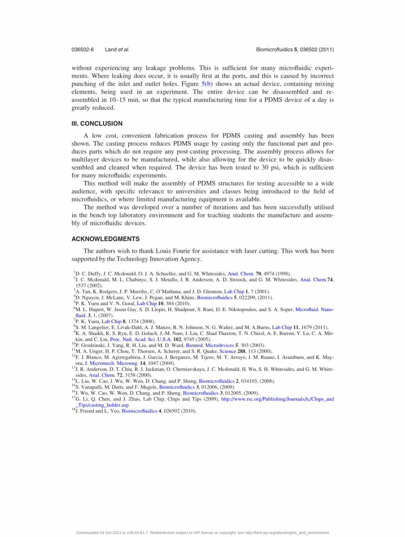
without experiencing any leakage problems. This is sufficient for many microfluidic experi-
ments. Where leaking does occur, it is usually first at the ports, and this is caused by incorrect
punching of the inlet and outlet holes. Figure 5(b) shows an actual device, containing mixing
elements, being used in an experiment. The entire device can be disassembled and re-
assembled in 10–15 min, so that the typical manufacturing time for a PDMS device of a day is
greatly reduced.
III. CONCLUSION
A low cost, convenient fabrication process for PDMS casting and assembly has been
shown. The casting process reduces PDMS usage by casting only the functional part and pro-
duces parts which do not require any post-casting processing. The assembly process allows for
multilayer devices to be manufactured, while also allowing for the device to be quickly disas-
sembled and cleaned when required. The device has been tested to 30 psi, which is sufficient
for many microfluidic experiments.
This method will make the assembly of PDMS structures for testing accessible to a wide
audience, with specific relevance to universities and classes being introduced to the field of
microfluidics, or where limited manufacturing equipment is available.
The method was developed over a number of iterations and has been successfully utilised
in the bench top laboratory environment and for teaching students the manufacture and assem-
bly of microfluidic devices.
ACKNOWLEDGMENTS
The authors wish to thank Louis Fourie for assistance with laser cutting. This work has been
supported by the Technology Innovation Agency.
1D. C. Duffy, J. C. Mcdonald, O. J. A. Schueller, and G. M. Whitesides, Anal. Chem. 70, 4974 (1998).2J. C. Mcdonald, M. L. Chabinyc, S. J. Metallo, J. R. Anderson, A. D. Stroock, and G. M. Whitesides, Anal. Chem.74,1537 (2002).
3A. Tan, K. Rodgers, J. P. Murrihy, C. O’Mathuna, and J. D. Glennon, Lab Chip 1, 7 (2001).4D. Nguyen, J. McLane, V. Lew, J. Pegan, and M. Khine, Biomicrofluidics 5, 022209, (2011).5P. K. Yuen and V. N. Goral, Lab Chip 10, 384 (2010).6M. L. Hupert, W. Jason Guy, S. D. Llopis, H. Shadpour, S. Rani, D. E. Nikitopoulos, and S. A. Soper, Microfluid. Nano-fluid. 3, 1, (2007).
7P. K. Yuen, Lab Chip 8, 1374 (2008).8S. M. Langelier, E. Livak-Dahl, A. J. Manzo, B. N. Johnson, N. G. Walter, and M. A.Burns, Lab Chip 11, 1679 (2011).9K. A. Shaikh, K. S. Ryu, E. D. Goluch, J.-M. Nam, J. Liu, C. Shad Thaxton, T. N. Chiesl, A. E. Barron, Y. Lu, C. A. Mir-kin, and C. Liu, Proc. Natl. Acad. Sci. U.S.A. 102, 9745 (2005).
10P. Grodzinski, J. Yang, R. H. Liu, and M. D. Ward, Biomed. Microdevices 5, 303 (2003).11M. A. Unger, H. P. Chou, T. Thorsen, A. Scherer, and S. R. Quake, Science 288, 113 (2000).12F. J. Blanco, M. Agirregabiria, J. Garcia, J. Berganzo, M. Tijero, M. T. Arroyo, J. M. Ruano, I. Aramburu, and K. May-
ora, J. Micromech. Microeng. 14, 1047 (2004).13J. R. Anderson, D. T. Chiu, R. J. Jackman, O. Cherniavskaya, J. C. Mcdonald, H. Wu, S. H. Whitesides, and G. M. White-
sides, Anal. Chem. 72, 3158 (2000).14L. Liu, W. Cao, J. Wu, W. Wen, D. Chang, and P. Sheng, Biomicrofluidics 2, 034103, (2008).15S. Vanapalli, M. Duits, and F. Mugele, Biomicrofluidics 3, 012006, (2009).16J. Wu, W. Cao, W. Wen, D. Chang, and P. Sheng, Biomicrofluidics 3, 012005, (2009).17G. Li, Q. Chen, and J. Zhao, Lab Chip, Chips and Tips (2009), http://www.rsc.org/Publishing/Journals/lc/Chips_and
_Tips/casting_holder.asp.18J. Friend and L. Yeo, Biomicrofluidics 4, 026502 (2010).
036502-6 Land et al. Biomicrofluidics 5, 036502 (2011)
Downloaded 18 Oct 2011 to 146.64.81.7. Redistribution subject to AIP license or copyright; see http://bmf.aip.org/about/rights_and_permissions