Embed Size (px)
Citation preview

Electron Transport in Multigate InxGa1−x As Nanowire FETs: FromDiffusive to Ballistic Regimes at Room TemperatureArun V. Thathachary,* Nidhi Agrawal, Lu Liu, and Suman Datta*
Electrical Engineering Department, The Pennsylvania State University, University Park, Pennsylvania 16802, United States
*S Supporting Information
ABSTRACT: The III−V semiconductors such as InxGa1‑xAs(x = 0.53−0.70) have attracted significant interest in thecontext of low power digital complementary metal-oxide-semiconductor (CMOS) technology due to their superiortransport properties. However, top-down patterning of III−Vsemiconductor thin films into strongly confined quasi-one-dimensional (1D) nanowire geometries can potentiallydegrade the transport properties. To date, few reports existregarding transport measurement in multigate nanowirestructures. In this work, we report a novel methodology forcharacterizing electron transport in III−V multigate nanowirefield effect transistors (NWFETs). We demonstrate multigateNWFETs integrated with probe electrodes in Hall Bridge geometry to enable four-point measurements of both longitudinal andtransverse resistance. This allows for the first time accurate extraction of Hall mobility and its dependence on carrierconcentration in III−V NWFETs. Furthermore, it is shown that by implementing parallel arrays of nanowires, it is possible toenhance the signal-to-noise ratio of the measurement, enabling more reliable measurement of Hall voltage (carrierconcentration) and, hence, mobility. We characterize the mobility for various nanowire widths down to 40 nm and observe amonotonic reduction in mobility compared to planar devices. Despite this reduction, III−V NWFET mobility is shown tooutperform state-of-the-art strained silicon NWFETs. Finally, we demonstrate evidence of room -temperature ballistic transport,a desirable property in the context of short channel transistors, in strongly confined III−V nanowire junctions using magneto-transport measurements in a nanoscale Hall-cross structure.
KEYWORDS: Field effect transistor, Hall effect, Hall cross, multigate FET, III−V, nanowire FET CMOS, scattering,electrical transport, diffusive transport, ballistic transport
Power constrained scaling of complementary metal oxidesemiconductor (CMOS) technology places several strin-
gent requirements on the performance metrics of theunderlying device, such as drive-current, leakage current, on-to-off state current ratio, subthreshold slope, drain-inducedbarrier lowering, which have to be satisfied simultaneously.1,2 Akey requirement however, is to reduce dynamic powerdissipation. This can be achieved by scaling down the supplyvoltage (Vdd) because that power dissipation is proportional tothe square of Vdd. At reduced supply voltages, however,traditional silicon CMOS is limited by reduced drive currents.In this context, III−V material systems are being activelyresearched because they afford competitive drive currents atlower supply voltages.3−5 This advantage stems primarily fromthe reduced effective mass in low band gap III−V materials,which results in higher mobility.In order to take advantage of this high mobility while
maintaining a high ION/IOFF ratio, multigate architectures havebeen introduced to achieve better electrostatic integrity inhighly scaled transistors.6,7 However, confining III−V materialsto nanowire (NW) like structures, either by top-downpatterning or bottom-up growth, can result in additional
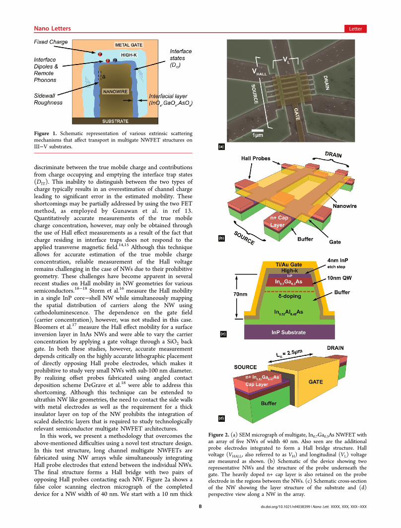
scattering mechanisms that are detrimental to electrontransport. Figure 1 shows a schematic illustration of thedifferent extrinsic scattering mechanisms that can arise in suchstructures. Among the various factors that influence themobility, the dominant mechanism in such structures is likelythe scattering from the side walls, and in recent years, there hasbeen significant interest in measuring and modeling thesevarious scattering mechanisms.8,9 It is therefore crucial tounderstand whether the advantage of good electrostatic controlin nanowire structures will come at the expense of reducedmobility, negating the benefits of using high mobility channelmaterials.Despite recent demonstrations of high-performance NW
based multigate devices including FETs and inverters,10,11 thereis a lack of quantitative understanding of the true carrierconcentration and mobility in such confined structures. Fieldeffect based mobility estimates have been reported for III−VNW and planar devices;9,12 however, this technique does not
Received: October 14, 2013Revised: December 20, 2013
Letter
pubs.acs.org/NanoLett
© XXXX American Chemical Society A dx.doi.org/10.1021/nl4038399 | Nano Lett. XXXX, XXX, XXX−XXX
discriminate between the true mobile charge and contributionsfrom charge occupying and emptying the interface trap states(DIT). This inability to distinguish between the two types ofcharge typically results in an overestimation of channel chargeleading to significant error in the estimated mobility. Theseshortcomings may be partially addressed by using the two FETmethod, as employed by Gunawan et al. in ref 13.Quantitatively accurate measurements of the true mobilecharge concentration, however, may only be obtained throughthe use of Hall effect measurements as a result of the fact thatcharge residing in interface traps does not respond to theapplied transverse magnetic field.14,15 Although this techniqueallows for accurate estimation of the true mobile chargeconcentration, reliable measurement of the Hall voltageremains challenging in the case of NWs due to their prohibitivegeometry. These challenges have become apparent in severalrecent studies on Hall mobility in NW geometries for varioussemiconductors.16−18 Storm et al.16 measure the Hall mobilityin a single InP core−shell NW while simultaneously mappingthe spatial distribution of carriers along the NW usingcathodoluminescence. The dependence on the gate field(carrier concentration), however, was not studied in this case.Bloomers et al.17 measure the Hall effect mobility for a surfaceinversion layer in InAs NWs and were able to vary the carrierconcentration by applying a gate voltage through a SiO2 backgate. In both these studies, however, accurate measurementdepends critically on the highly accurate lithographic placementof directly opposing Hall probe electrodes, which makes itprohibitive to study very small NWs with sub-100 nm diameter.By realizing offset probes fabricated using angled contactdeposition scheme DeGrave et al.18 were able to address thisshortcoming. Although this technique can be extended toultrathin NW like geometries, the need to contact the side wallswith metal electrodes as well as the requirement for a thickinsulator layer on top of the NW prohibits the integration ofscaled dielectric layers that is required to study technologicallyrelevant semiconductor multigate NWFET architectures.In this work, we present a methodology that overcomes the
above-mentioned difficulties using a novel test structure design.In this test structure, long channel multigate NWFETs arefabricated using NW arrays while simultaneously integratingHall probe electrodes that extend between the individual NWs.The final structure forms a Hall bridge with two pairs ofopposing Hall probes contacting each NW. Figure 2a shows afalse color scanning electron micrograph of the completeddevice for a NW width of 40 nm. We start with a 10 nm thick
Figure 1. Schematic representation of various extrinsic scatteringmechanisms that affect transport in multigate NWFET structures onIII−V substrates.
Figure 2. (a) SEM micrograph of multigate, In0.7Ga0.3As NWFET withan array of five NWs of width 40 nm. Also seen are the additionalprobe electrodes integrated to form a Hall bridge structure. Hallvoltage (VHALL, also referred to as VH) and longitudinal (VL) voltageare measured as shown. (b) Schematic of the device showing tworepresentative NWs and the structure of the probe underneath thegate. The heavily doped n+ cap layer is also retained on the probeelectrode in the regions between the NWs. (c) Schematic cross-sectionof the NW showing the layer structure of the substrate and (d)perspective view along a NW in the array.
Nano Letters Letter
dx.doi.org/10.1021/nl4038399 | Nano Lett. XXXX, XXX, XXX−XXXB

In0.7Ga0.3As quantum well (QW) channel grown by molecularbeam epitaxy (MBE) on semi-insulating InP substrate. A 4 nmthick InP etch stop layer and 20 nm thick heavily doped n-typeIn0.53Ga0.47As layer are grown on top of the quantum well tofacilitate ohmic contacts to the metal electrodes. The n+ caplayer is first recessed, using a wet etch comprising citric acid andH2O2, in order to define the channel region. The etch mask iscreated by opening windows, using e-beam lithography, indiluted ZEP 520A resist to define the recess etch openings overthe regions where nanowires will subsequently be patterned.The spacing between consecutive NWs in the array is kept at500 nm. Accounting for the 50 nm undercut from each sideresulting from the wet etch, we leave behind 400 nm of heavilydoped cap layer on the Hall probes in the regions between theNWs as seen in Figure 2b.We retain the cap layer in theseregions in order to maintain low resistance on the probes.Subsequently the entire structure comprising of the source/drain electrodes, NW array, and Hall probe electrodes ispatterned using e-beam lithography followed by dry etching ina chlorine (Cl) based plasma. This is followed by atomic layerdeposition (ALD) of 1 nm Al2O3 and 3 nm HfO2 high-kdielectric stack followed by Ti/Au gate metal electrodes,patterned using evaporation and lift-off process. The crosssection of the NW is shown schematically in Figure 2c. Finally,a second metal stack comprising of Ti/Au is deposited on the n+ cap using lift-off to form the source/drain pads. Figure 2dprovides a three-dimensional perspective view of the gatednanowire region.We fabricate devices with various NW widths starting from 1
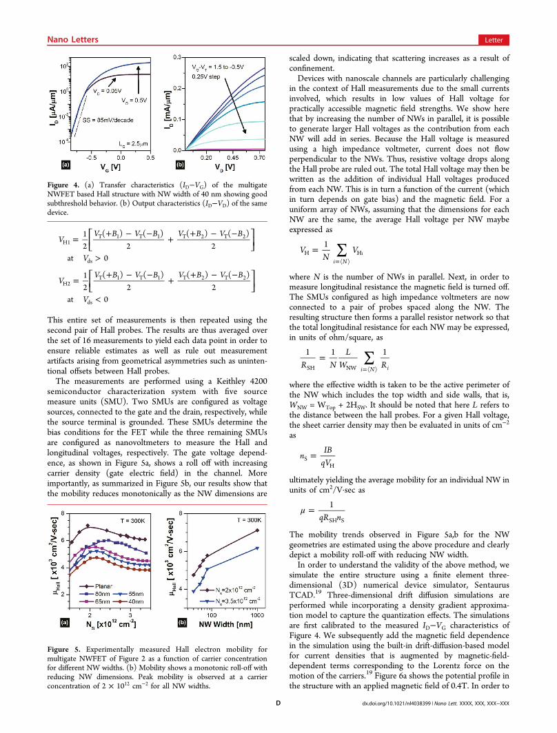
μm (plate type geometry) down to 40 nm in order to create toa 1D confined geometry. The gate lengths for all the teststructures are kept constant at 2.5 μm while maintaining asource to drain separation of 4 μm and Hall probe separation of1.5 μm. The quality and morphology of the side walls of thetop-down etched structures is of utmost importance as thisdirectly impacts the transport properties through the scatteringmechanisms delineated earlier in Figure 1. We analyze thecross−section of the etched NWs through transmissionelectron microscopy (TEM) and electron energy loss spec-troscopy (EELS) as shown in Figure 3. The side wall shows asmooth etch profile without any visible damage to the NW.However, we see that a thin (∼1 nm) indium rich native oxidelayer is left behind after etching. This layer is etchedsubsequently using a dilute sulfuric acid treatment prior todeposition of high-k dielectric. The resulting interface has goodelectrical properties as evidenced by NWFET characteristicsshown in Figure 4. The measured transfer characteristics for thelong channel array device with 40 nm NW width shows asubthreshold slope of 85 mV/dec. Close to zero drain-inducedbarrier lowering (DIBL) indicates good electrical isolationbetween source and drain pads for the In0.7Ga0.3As quantumwell structure, aided by the presence of InAlAs barrier layer.Further, the output characteristics show good saturation with apeak drive current of around 250 μA/μm.After ensuring good FET transfer characteristics for the test
structure, we perform gated Hall measurements. The Hallmeasurements are performed in a Lakeshore TTP6 cryogenicprobe station equipped with a superconducting magnet that cangenerate magnetic fields up to 2.5T. The magnetic field isoriented perpendicular to the substrate for all the measure-ments carried out in this study. We point out here that since thetest structures are FETs constructed in a Hall bridge geometry,it is possible to change carrier concentration in a well-
controlled fashion using gate modulation. The gate voltage(Vgs) is varied from −0.5 to 1 V in steps of 50 mV, whileapplying a fixed source to drain bias (Vds) of 50 mV. The Hallvoltage (VH) is then recorded at magnetic field values of ±0.5and ±0.8T for each gate bias, and the measurements are thenrepeated after reversing the polarity of Vds. Thus the Hallvoltage from each pair of probes is written as
=+
VV V( )
2HH1 H2
where
Figure 3. Characterization of the top down patterned nanowiresubsequent to plasma etching: (a) STEM image indicating location ofEELS line scan and (b) results of EELS line scan showing possibleformation of indium oxide interfacial layer. (c) EELS elemental map ofNW cross-section confirming that top-down etch yields high quality,defect-free NW structure, while also highlighting the formation ofnative oxide layer on side walls.
Nano Letters Letter
dx.doi.org/10.1021/nl4038399 | Nano Lett. XXXX, XXX, XXX−XXXC
=+ − −
++ − −
>
=+ − −
++ − −
<
⎡⎣⎢
⎤⎦⎥
⎡⎣⎢
⎤⎦⎥
VV B V B V B V B
V
VV B V B V B V B
V
12
( ) ( )2
( ) ( )2
at 0
12
( ) ( )2
( ) ( )2
at 0
H1T 1 T 1 T 2 T 2
ds
H2T 1 T 1 T 2 T 2
ds
This entire set of measurements is then repeated using thesecond pair of Hall probes. The results are thus averaged overthe set of 16 measurements to yield each data point in order toensure reliable estimates as well as rule out measurementartifacts arising from geometrical asymmetries such as uninten-tional offsets between Hall probes.The measurements are performed using a Keithley 4200
semiconductor characterization system with five sourcemeasure units (SMU). Two SMUs are configured as voltagesources, connected to the gate and the drain, respectively, whilethe source terminal is grounded. These SMUs determine thebias conditions for the FET while the three remaining SMUsare configured as nanovoltmeters to measure the Hall andlongitudinal voltages, respectively. The gate voltage depend-ence, as shown in Figure 5a, shows a roll off with increasingcarrier density (gate electric field) in the channel. Moreimportantly, as summarized in Figure 5b, our results show thatthe mobility reduces monotonically as the NW dimensions are
scaled down, indicating that scattering increases as a result ofconfinement.Devices with nanoscale channels are particularly challenging
in the context of Hall measurements due to the small currentsinvolved, which results in low values of Hall voltage forpractically accessible magnetic field strengths. We show herethat by increasing the number of NWs in parallel, it is possibleto generate larger Hall voltages as the contribution from eachNW will add in series. Because the Hall voltage is measuredusing a high impedance voltmeter, current does not flowperpendicular to the NWs. Thus, resistive voltage drops alongthe Hall probe are ruled out. The total Hall voltage may then bewritten as the addition of individual Hall voltages producedfrom each NW. This is in turn a function of the current (whichin turn depends on gate bias) and the magnetic field. For auniform array of NWs, assuming that the dimensions for eachNW are the same, the average Hall voltage per NW maybeexpressed as
∑==
VN
V1
i NiH H
where N is the number of NWs in parallel. Next, in order tomeasure longitudinal resistance the magnetic field is turned off.The SMUs configured as high impedance voltmeters are nowconnected to a pair of probes spaced along the NW. Theresulting structure then forms a parallel resistor network so thatthe total longitudinal resistance for each NW may be expressed,in units of ohm/square, as
∑==R N
LW R
1 1 1
i N iSH NW
where the effective width is taken to be the active perimeter ofthe NW which includes the top width and side walls, that is,WNW = WTop + 2HSW. It should be noted that here L refers tothe distance between the hall probes. For a given Hall voltage,the sheet carrier density may then be evaluated in units of cm−2
as
=nIB
qVSH
ultimately yielding the average mobility for an individual NW inunits of cm2/V·sec as
μ =qR n
1
SH S
The mobility trends observed in Figure 5a,b for the NWgeometries are estimated using the above procedure and clearlydepict a mobility roll-off with reducing NW width.In order to understand the validity of the above method, we
simulate the entire structure using a finite element three-dimensional (3D) numerical device simulator, SentaurusTCAD.19 Three-dimensional drift diffusion simulations areperformed while incorporating a density gradient approxima-tion model to capture the quantization effects. The simulationsare first calibrated to the measured ID−VG characteristics ofFigure 4. We subsequently add the magnetic field dependencein the simulation using the built-in drift-diffusion-based modelfor current densities that is augmented by magnetic-field-dependent terms corresponding to the Lorentz force on themotion of the carriers.19 Figure 6a shows the potential profile inthe structure with an applied magnetic field of 0.4T. In order to
Figure 4. (a) Transfer characteristics (ID−VG) of the multigateNWFET based Hall structure with NW width of 40 nm showing goodsubthreshold behavior. (b) Output characteristics (ID−VD) of the samedevice.
Figure 5. Experimentally measured Hall electron mobility formultigate NWFET of Figure 2 as a function of carrier concentrationfor different NW widths. (b) Mobility shows a monotonic roll-off withreducing NW dimensions. Peak mobility is observed at a carrierconcentration of 2 × 1012 cm−2 for all NW widths.
Nano Letters Letter
dx.doi.org/10.1021/nl4038399 | Nano Lett. XXXX, XXX, XXX−XXXD
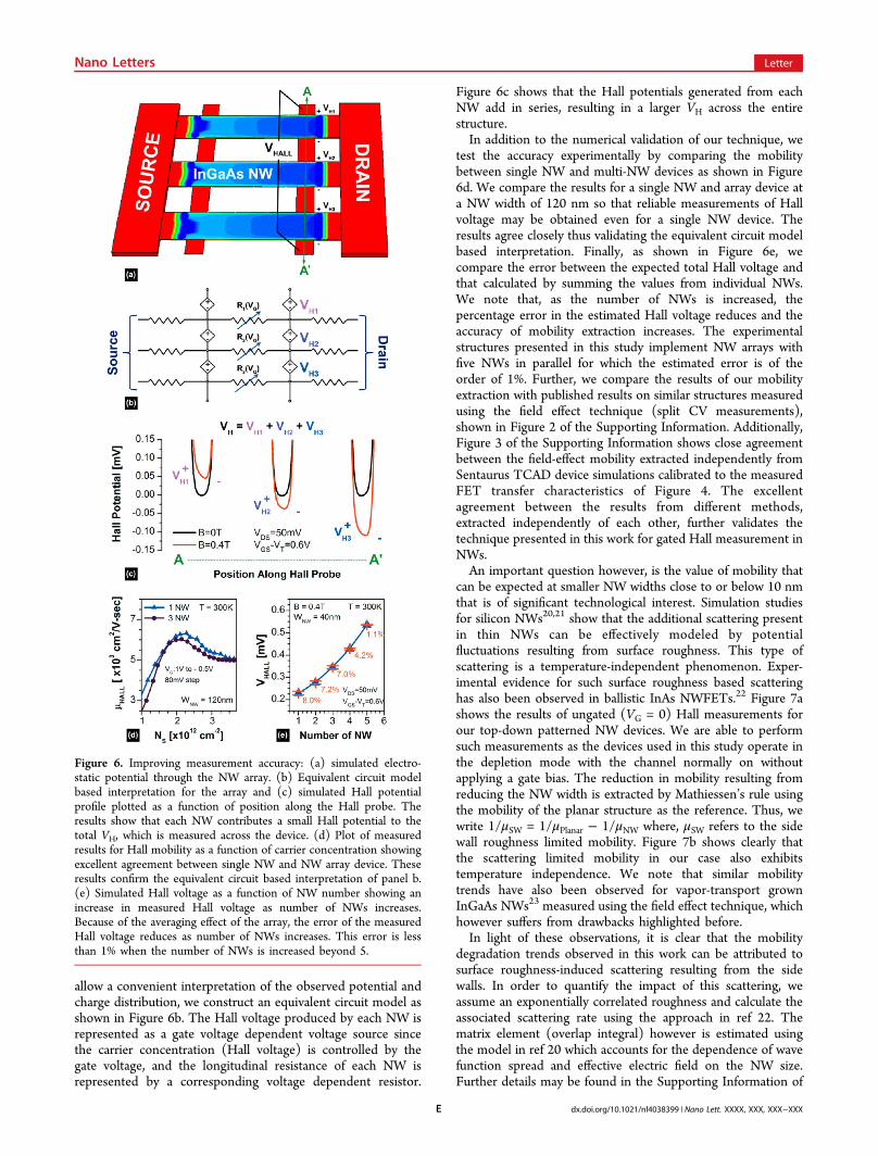
allow a convenient interpretation of the observed potential andcharge distribution, we construct an equivalent circuit model asshown in Figure 6b. The Hall voltage produced by each NW isrepresented as a gate voltage dependent voltage source sincethe carrier concentration (Hall voltage) is controlled by thegate voltage, and the longitudinal resistance of each NW isrepresented by a corresponding voltage dependent resistor.
Figure 6c shows that the Hall potentials generated from eachNW add in series, resulting in a larger VH across the entirestructure.In addition to the numerical validation of our technique, we
test the accuracy experimentally by comparing the mobilitybetween single NW and multi-NW devices as shown in Figure6d. We compare the results for a single NW and array device ata NW width of 120 nm so that reliable measurements of Hallvoltage may be obtained even for a single NW device. Theresults agree closely thus validating the equivalent circuit modelbased interpretation. Finally, as shown in Figure 6e, wecompare the error between the expected total Hall voltage andthat calculated by summing the values from individual NWs.We note that, as the number of NWs is increased, thepercentage error in the estimated Hall voltage reduces and theaccuracy of mobility extraction increases. The experimentalstructures presented in this study implement NW arrays withfive NWs in parallel for which the estimated error is of theorder of 1%. Further, we compare the results of our mobilityextraction with published results on similar structures measuredusing the field effect technique (split CV measurements),shown in Figure 2 of the Supporting Information. Additionally,Figure 3 of the Supporting Information shows close agreementbetween the field-effect mobility extracted independently fromSentaurus TCAD device simulations calibrated to the measuredFET transfer characteristics of Figure 4. The excellentagreement between the results from different methods,extracted independently of each other, further validates thetechnique presented in this work for gated Hall measurement inNWs.An important question however, is the value of mobility that
can be expected at smaller NW widths close to or below 10 nmthat is of significant technological interest. Simulation studiesfor silicon NWs20,21 show that the additional scattering presentin thin NWs can be effectively modeled by potentialfluctuations resulting from surface roughness. This type ofscattering is a temperature-independent phenomenon. Exper-imental evidence for such surface roughness based scatteringhas also been observed in ballistic InAs NWFETs.22 Figure 7ashows the results of ungated (VG = 0) Hall measurements forour top-down patterned NW devices. We are able to performsuch measurements as the devices used in this study operate inthe depletion mode with the channel normally on withoutapplying a gate bias. The reduction in mobility resulting fromreducing the NW width is extracted by Mathiessen’s rule usingthe mobility of the planar structure as the reference. Thus, wewrite 1/μSW = 1/μPlanar − 1/μNW where, μSW refers to the sidewall roughness limited mobility. Figure 7b shows clearly thatthe scattering limited mobility in our case also exhibitstemperature independence. We note that similar mobilitytrends have also been observed for vapor-transport grownInGaAs NWs23 measured using the field effect technique, whichhowever suffers from drawbacks highlighted before.In light of these observations, it is clear that the mobility
degradation trends observed in this work can be attributed tosurface roughness-induced scattering resulting from the sidewalls. In order to quantify the impact of this scattering, weassume an exponentially correlated roughness and calculate theassociated scattering rate using the approach in ref 22. Thematrix element (overlap integral) however is estimated usingthe model in ref 20 which accounts for the dependence of wavefunction spread and effective electric field on the NW size.Further details may be found in the Supporting Information of
Figure 6. Improving measurement accuracy: (a) simulated electro-static potential through the NW array. (b) Equivalent circuit modelbased interpretation for the array and (c) simulated Hall potentialprofile plotted as a function of position along the Hall probe. Theresults show that each NW contributes a small Hall potential to thetotal VH, which is measured across the device. (d) Plot of measuredresults for Hall mobility as a function of carrier concentration showingexcellent agreement between single NW and NW array device. Theseresults confirm the equivalent circuit based interpretation of panel b.(e) Simulated Hall voltage as a function of NW number showing anincrease in measured Hall voltage as number of NWs increases.Because of the averaging effect of the array, the error of the measuredHall voltage reduces as number of NWs increases. This error is lessthan 1% when the number of NWs is increased beyond 5.
Nano Letters Letter
dx.doi.org/10.1021/nl4038399 | Nano Lett. XXXX, XXX, XXX−XXXE
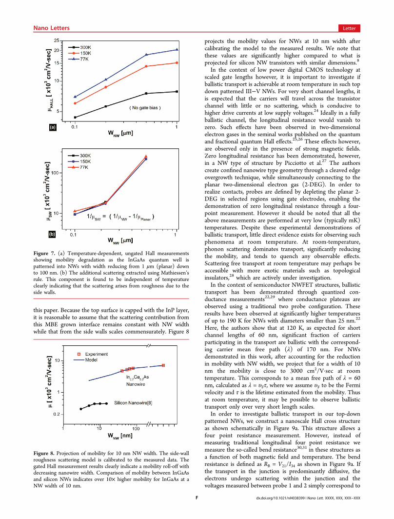
this paper. Because the top surface is capped with the InP layer,it is reasonable to assume that the scattering contribution fromthis MBE grown interface remains constant with NW widthwhile that from the side walls scales commensurately. Figure 8
projects the mobility values for NWs at 10 nm width aftercalibrating the model to the measured results. We note thatthese values are significantly higher compared to what isprojected for silicon NW transistors with similar dimensions.8
In the context of low power digital CMOS technology atscaled gate lengths however, it is important to investigate ifballistic transport is achievable at room temperature in such topdown patterned III−V NWs. For very short channel lengths, itis expected that the carriers will travel across the transistorchannel with little or no scattering, which is conducive tohigher drive currents at low supply voltages.24 Ideally in a fullyballistic channel, the longitudinal resistance would vanish tozero. Such effects have been observed in two-dimensionalelectron gases in the seminal works published on the quantumand fractional quantum Hall effects.25,26 These effects however,are observed only in the presence of strong magnetic fields.Zero longitudinal resistance has been demonstrated, however,in a NW type of structure by Picciotto et al.27 The authorscreate confined nanowire type geometry through a cleaved edgeovergrowth technique, while simultaneously connecting to theplanar two-dimensional electron gas (2-DEG). In order torealize contacts, probes are defined by depleting the planar 2-DEG in selected regions using gate electrodes, enabling thedemonstration of zero longitudinal resistance through a four-point measurement. However it should be noted that all theabove measurements are performed at very low (typically mK)temperatures. Despite these experimental demonstrations ofballistic transport, little direct evidence exists for observing suchphenomena at room temperature. At room-temperature,phonon scattering dominates transport, significantly reducingthe mobility, and tends to quench any observable effects.Scattering free transport at room temperature may perhaps beaccessible with more exotic materials such as topologicalinsulators,28 which are actively under investigation.In the context of semiconductor NWFET structures, ballistic
transport has been demonstrated through quantized con-ductance measurements22,29 where conductance plateaus areobserved using a traditional two probe configuration. Theseresults have been observed at significantly higher temperaturesof up to 190 K for NWs with diameters smaller than 25 nm.22
Here, the authors show that at 120 K, as expected for shortchannel lengths of 60 nm, significant fraction of carriersparticipating in the transport are ballistic with the correspond-ing carrier mean free path (λ) of 170 nm. For NWsdemonstrated in this work, after accounting for the reductionin mobility with NW width, we project that for a width of 10nm the mobility is close to 3000 cm2/V·sec at roomtemperature. This corresponds to a mean free path of λ = 60nm, calculated as λ = υFτ, where we assume υF to be the Fermivelocity and τ is the lifetime estimated from the mobility. Thusat room temperature, it may be possible to observe ballistictransport only over very short length scales.In order to investigate ballistic transport in our top-down
patterned NWs, we construct a nanoscale Hall cross structureas shown schematically in Figure 9a. This structure allows afour point resistance measurement. However, instead ofmeasuring traditional longitudinal four point resistance wemeasure the so-called bend resistance30,31 in these structures asa function of both magnetic field and temperature. The bendresistance is defined as RB = V21/I34 as shown in Figure 9a. Ifthe transport in the junction is predominantly diffusive, theelectrons undergo scattering within the junction and thevoltages measured between probe 1 and 2 simply correspond to
Figure 7. (a) Temperature-dependent, ungated Hall measurementsshowing mobility degradation as the InGaAs quantum well ispatterned into NWs with width reducing from 1 μm (planar) downto 100 nm. (b) The additional scattering extracted using Mathiessen’srule. This component is found to be independent of temperatureclearly indicating that the scattering arises from roughness due to theside walls.
Figure 8. Projection of mobility for 10 nm NW width. The side-wallroughness scattering model is calibrated to the measured data. Thegated Hall measurement results clearly indicate a mobility roll-off withdecreasing nanowire width. Comparison of mobility between InGaAsand silicon NWs indicates over 10× higher mobility for InGaAs at aNW width of 10 nm.
Nano Letters Letter
dx.doi.org/10.1021/nl4038399 | Nano Lett. XXXX, XXX, XXX−XXXF
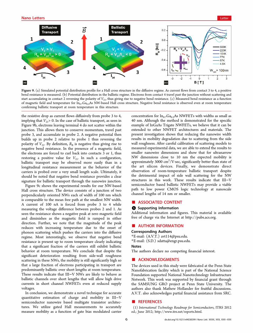
the resistive drop as current flows diffusively from probe 3 to 4,implying that V21> 0. In the case of ballistic transport, as seen inFigure 9b, electrons leaving terminal 4 do not scatter within thejunction. This allows them to conserve momentum, travel pastprobe 3, and accumulate in probe 2. A negative potential thenbuilds up in probe 2 relative to probe 1 thus reversing thepolarity of V21. By definition, RB is negative thus giving rise tonegative bend resistance. In the presence of a magnetic field,the electrons are forced to curl back into contacts 3 or 1, thusrestoring a positive value for V21. In such a configuration,ballistic transport may be observed more easily than in alongitudinal resistance measurement as the behavior of thecarriers is probed over a very small length scale. Ultimately, itshould be noted that negative bend resistance provides a clearsignature for ballistic transport through the nanowire junction.Figure 9c shows the experimental results for our NW-based
Hall cross structure. The device consists of a junction of twoperpendicularly oriented NWs each of width of 100 nm whichis comparable to the mean free path at the smallest NW width.A current of 100 nA is forced from probe 3 to 4 whilemeasuring the voltage difference between probes 2 and 1. Asseen the resistance shows a negative peak at zero magnetic fieldand diminishes as the magnetic field is ramped in eitherdirection. Further, we note that the magnitude of the peakreduces with increasing temperature due to the onset ofphonon scattering which pushes the carriers into the diffusiveregime. Most interestingly, we observe that negative bendresistance is present up to room temperature clearly indicatingthat a significant fraction of the carriers still exhibit ballisticbehavior at room temperature. We conclude that despite thesignificant deterioration resulting from side-wall roughnessscattering in these NWs, the mobility is still significantly high sothat a large fraction of electrons participating in transport arepredominantly ballistic over short lengths at room temperature.These results indicate that III−V NWs are likely to behave asballistic channels over short lengths that will allow high drivecurrents in short channel NWFETs even at reduced supplyvoltages.In conclusion, we demonstrate a novel technique for accurate
quantitative estimation of charge and mobility in III−Vsemiconductor nanowire based multigate transistor architec-tures. We utilize gated Hall measurements to accuratelymeasure mobility as a function of gate bias modulated carrier
concentration for In0.7Ga0.3As NWFETs with widths as small as40 nm. Although the method is demonstrated for the specificexample of InGaAs Trigate NWFETs, we believe that it can beextended to other NWFET architectures and materials. Thepresent investigation shows that reducing the nanowire widthresults in mobility degradation due to scattering from the sidewall roughness. After careful calibration of scattering models tomeasured experimental data, we are able to extend the results tosmaller nanowire dimensions and show that for ultranarrowNW dimensions close to 10 nm the expected mobility isapproximately 3000 cm2/V·sec, significantly better than state ofthe art silicon devices. Finally, we demonstrate directobservation of room-temperature ballistic transport despitethe detrimental impact of side wall scattering for the NWstructures in this work. These results indicate that III−Vsemiconductor based ballistic NWFETs may provide a viablepath to low power CMOS logic technology at nanoscalechannel lengths of 14 nm or smaller.
■ ASSOCIATED CONTENT*S Supporting InformationAdditional information and figures. This material is availablefree of charge via the Internet at http://pubs.acs.org.
■ AUTHOR INFORMATIONCorresponding Authors*E-mail: (A.V.T.) [email protected].*E-mail: (S.D.) [email protected] authors declare no competing financial interest.
■ ACKNOWLEDGMENTSThe devices used in this study were fabricated at the Penn StateNanofabrication facility which is part of the National ScienceFoundation supported National Nanotechnology InfrastructureNetwork. This work was supported by financial grant throughthe SAMSUNG GRO project at Penn State University. Theauthors also thank Mathew Hollander for fruitful discussions.A.V.T. also acknowledges partial financial assistance from SRC.
■ REFERENCES(1) International Technology Roadmap for Semiconductors, ITRS 2012ed.; June 2012; http://www.itrs.net/reports.html.
Figure 9. (a) Simulated potential distribution profile for a Hall cross structure in the diffusive regime. As current flows from contact 3 to 4, a positivebend resistance is measured. (b) Potential distribution in the ballistic regime. Electrons from contact 4 travel past the junction without scattering andstart accumulating in contact 2 reversing the polarity of V21, thus giving rise to negative bend resistance. (c) Measured bend resistance as a functionof magnetic field and temperature for In0.7Ga0.3As NW-based Hall cross structure. Negative bend resistance is observed even at room temperatureconfirming ballistic transport at room temperature in this structure.
Nano Letters Letter
dx.doi.org/10.1021/nl4038399 | Nano Lett. XXXX, XXX, XXX−XXXG
(2) Chau, R.; Datta, S.; Doczy, M.; Doyle, B.; Jin, B.; Kavalieros, J.;Majumdar, A. Benchmarking nanotechnology for high-performanceand low-power logic transistor applications. IEEE Trans. Nanotechnol.2005, 4 (No. 2), 153−158.(3) Lundstrom, M. Science 2003, 299, 210−211.(4) del Alamo, J. A. Nanometre-scale electronics with III−Vcompound semiconductors. Nature 2011, 479, 317−323.(5) Dewey, G.; Hudait, M. K.; Lee, K.; Pillarisetty, R.; Rachmady, W.;Radosavljevic, M.; et al. Carrier transport in high-mobility III−Vquantum-well transistors and performance impact for high-speed low-power logic applications. IEEE Electron Device Lett. 2008, 29 (10),1094−1097.(6) Radosavljevic, M.; Dewey, G.; Basu, D.; Boardman, J.; Chu-Kung,B.; Fastenau, J. M.; Kabehie, S.; Kavalieros, J.; et al. ElectrostaticsImprovement in 3-D Tri-gate Over Ultra-Thin Body Planar InGaAsQuantum Well Field Effect Transistors with High-K Gate Dielectricand Scaled Gate-to-Drain/Gate-to-Source Separation. Int. ElectronDevices Meet. 2011, 33.1.1−33.1.4.(7) Gu, J. J.; Wang, X. W.; Wu, H.; Shao, J.; Neal, A. T.; Manfra, M.J.; Gordon, R. G.; Ye, P. D. 20−80nm Channel Length InGaAs Gate-all-around Nanowire MOSFETs with EOT=1.2nm and LowestSS=63mV/dec. Int. Electron Devices Meet. 2012, 27.6.1−27.6.4.(8) Kotlyar, R.; Obradovic, B.; Matagne, P.; Stettler, M.; Giles, M. D.Assessment of room-temperature phonon-limited mobility in gatedsilicon nanowires. Appl. Phys. Lett. 2004, 84 (25), 5270−5272.(9) Ford, A. C.; Ho, J. C.; Chueh, Y.-L.; Tseng, Y.-C.; Fan, Z.; Guo,J.; Bokor, J.; Javey, A. Diameter-Dependent Electron Mobility of InAsNanowires. Nano Lett. 2009, 9 (1), 360−365.(10) Tomioka, k.; Yoshimura, M.; Fukui, T. A III−V nanowirechannel on silicon for high-performance vertical transistors. Nature2012, 488, 189−192.(11) Dey, A. W.; Svensson, J.; Borg, B. M.; Ek, M.; Wernersson, L.-E.Single InAs/GaSb Nanowire Low-Power CMOS Inverter. Nano Lett.2012, 12, 5593−5597.(12) Lin, J.; Antoniadis, D. A.; del Alamo, J. A. Sub-30 nm InAsQuantum-Well MOSFETs with Self-aligned Metal Contacts and Sub-1nm EOT HfO2 Insulator. Int. Electron Devices Meet. 2012, 32.1.1−32.1.4.(13) Gunawan, O.; Sekaric, L.; Majumdar, A.; Rooks, M.;Appenzeller, J.; Sleight, J. W.; Guha, S.; Haensch, W. Measurementof Carrier Mobility in Silicon Nanowires. Nano Lett. 2008, 8 (6),1566−1571.(14) Shahrjerdi, D.; Nah, J.; Hekmatshoar, B.; Akyol, T.; Ramon, M.;Tutuc, E.; Banerjee, S. K. Hall mobility measurements in enhance-ment-mode GaAs field-effect transistors with Al2O3 gate dielectric.Appl. Phys. Lett. 2010, 97, 213506.(15) Veksler, D.; Nagaiah, P.; Chidambaram, T.; Cammarere, R.;Tokranov, V.; Yakimov, M.; Chen, Y.-T.; Huang, J.; Goel, N.; Oh, J.;Bersuker, G.; Hobbs, C.; Kirsch, P. D.; Oktyabrsky, S. Quantificationof interfacial state density (Dit) at the high-k/III-V interface based onHall effect measurements. J. Appl. Phys. 2012, 112, 054504.(16) Storm, K.; Halvardsson, F.; Heurlin, M.; Lindgren, D.;Gustafsson, A.; Wu, P. M.; Monemar, B.; Samuelson, L. Spatiallyresolved Hall effect measurement in asingle semiconductor nanowire.Nat. Nanotechnol. 2012, 7, 718−722.(17) Blomers, Ch.; Grap, T.; Lepsa, M. I.; Moers, J.; Trellenkamp,St.; Grutzmacher, D.; Luth, H. Schapers, Th. Hall effect measurementson InAs nanowires. Appl. Phys. Lett. 2012, 101, 152106.(18) DeGrave, J. P.; Liang, D.; Jin, S. A General Method to Measurethe Hall Effect in Nanowires: Examples of FeS2 and MnSi. Nano Lett.2013, 13, 2704−2709.(19) Sentaurus Device User Guide, version f-2011.09 ed.; Synopsys,Inc., 2011; http://www.synopsys.com/Tools/TCAD.(20) Ramayya, E. B.; Vasileska, D.; Goodnick, S. M.; Knezevic, I. J.Appl. Phys. 2008, 104, 063711.(21) Poli, S.; Pala, M. G.; Poiroux, T.; Deleonibus, S.; Baccarani, G.Size Dependence of Surface-Roughness-Limited Mobility in Silicon-Nanowire FETs. IEEE Trans. Electron Devices 2008, 55 (11), 2968−2975.
(22) Chuang, S.; Gao, Q.; Kapadia, R.; Ford, A. C.; Guo, J.; Javey, A.Ballistic InAs Nanowire Transistors. Nano Lett. 2013, 13, 555−558.(23) Hou, J. J.; Wang, F.; Han, N.; Zhu, H.; Fok, K.; et al. Diameterdependence of electron mobility in InGaAs nanowires. Appl. Phys. Lett.2013, 102, 093112.(24) Wang, J.; Lundstrom, M. Ballistic Transport in High ElectronMobility Transistors. IEEE Trans. Electron Devices 2003, 50 (7), 1604−1609.(25) von-klitzing, K.; Dorda, G.; Pepper, M. New Method for High-Accuracy Determination of the Fine-Structure Constant Based onQuantized Hall Resistance. Phys. Rev. Lett. 1980, 45, 494−497.(26) Tsui, D. C.; Stormer, H. L.; Gossard, A. C. Two-DimensionalMagnetotransport in the Extreme Quantum Limit. Phys. Rev. Lett.1980, 48, 1559−1562.(27) de Picciotto, R.; Stormer, H. L.; Pfeiffer, L. N.; Baldwin, K. W.;West, K. W. Four-terminal resistance of a ballistic quantum wire.Nature 2001, 411, 51−53.(28) Hasan, M. Z.; kane, C. L. Topological insulators. Rev. Mod. Phys.2010, 82, 3045−3067.(29) Javey, A.; Guo, J.; Wang, Q.; Lundstrom, M.; Dai, H. BallisticCarbon Nanotube Transistors. Nature 2003, 424, 654−657.(30) Gilbertson, A. M.; Fearn, M.; Kormanyos, A.; Read, D. E.;Lambert, C. J.; Emeny, M. T.; Ashley, T.; Solin, S. A.; Cohen, L. F.Phys. Rev. B 2011, 83, 075304.(31) Mayorov, A. S.; Gorbachev, R. V.; Morozov, S. V.; Britnell, L.;Jalil, R.; Ponomarenko, L. A.; Blake, P.; Novoselov, K. S.; Watanabe,K.; Taniguchi, T.; Geim, A. K. Nano Lett. 2011, 11, 2396−2399.
Nano Letters Letter
dx.doi.org/10.1021/nl4038399 | Nano Lett. XXXX, XXX, XXX−XXXH