Embed Size (px)
Citation preview
Direct Imaging of p−n Junction in Core−Shell GaN WiresP. Tchoulfian,*,†,‡,§ F. Donatini,†,‡ F. Levy,†,§ A. Dussaigne,†,§ P. Ferret,†,§ and J. Pernot*,†,‡,∥
†Univ. Grenoble Alpes, F-38000 Grenoble, France‡CNRS, Inst. NEEL, F-38042 Grenoble, France§CEA, LETI, Minatec Campus, F-38054 Grenoble, France∥Institut Universitaire de France, F-75005 Paris, France
*S Supporting Information
ABSTRACT: While core−shell wire-based devices offer apromising path toward improved optoelectronic applications,their development is hampered by the present uncertaintyabout essential semiconductor properties along the three-dimensional (3D) buried p−n junction. Thanks to a cross-sectional approach, scanning electron beam probing techni-ques were employed here to obtain a nanoscale spatiallyresolved analysis of GaN core−shell wire p−n junctions grownby catalyst-free metal−organic vapor phase epitaxy on GaN and Si substrates. Both electron beam induced current (EBIC) andsecondary electron voltage constrast (VC) were demonstrated to delineate the radial and axial junction existing in the 3Dstructure. The Mg dopant activation process in p-GaN shell was dynamically controlled by the ebeam exposure conditions andvisualized thanks to EBIC mapping. EBIC measurements were shown to yield local minority carrier/exciton diffusion lengths onthe p-side (∼57 nm) and the n-side (∼15 nm) as well as depletion width in the range 40−50 nm. Under reverse bias conditions,VC imaging provided electrostatic potential maps in the vicinity of the 3D junction from which acceptor Na and donor Nd dopinglevels were locally determined to be Na = 3 × 1018 cm−3 and Nd = 3.5 × 1018 cm−3 in both the axial and the radial junction.Results from EBIC and VC are in good agreement. This nanoscale approach provides essential guidance to the furtherdevelopment of core−shell wire devices.KEYWORDS: GaN wire, core−shell p−n junction, doping level, diffusion length, electron beam induced current, voltage contrast
Wire-based devices have been considered as a promisingnew route toward improved electronic and optoelec-
tronic applications thanks to their desirable intrinsic propertiessuch as small footprints and improved strain relaxation.1−9 Inaddition, wire synthesis provides exciting new degrees offreedom for the fabrication of heterostructures with the adventof facet-selective shell growth.1 Along with a careful axial and/or radial design of doping levels and (alloy) compositions at thesingle wire level, an increased versatility is offered by wiredevices as compared to planar layer devices.1,6−11
The p−n junctions in wires with either axial4−6,11 or core−shell8−10,12,13 geometry have been reported to provide thebuilding block of optoelectronic applications. The lattergeometry leads to a three-dimensional (3D) core−shell p−njunction thanks to a shell generally deposited on both thesidewalls and the top of the core. Taking advantage of the wirehigh aspect ratio, this increases the active region area, animprovement that is expected to alleviate the efficiency droopissue in light-emitting devices (LEDs) and to increase lightabsorption in solar cells. Because GaN and its alloys are thematerials of choice for optoelectronic applications, III-Nitridesnano- and microwire core−shell devices have been focusingmuch attention.14 In the context of light emission, this interestis particularly driven by the use of the nonpolar facets (m-plane) as templates for the growth of multiple-quantum wells
yielding sidewall light emission free of polarization ef-fects.8,9,11,13,15,16
Similar to the planar epitaxial case, measurements of materialproperties such as doping levels and minority carrier (orexciton17) diffusion lengths are crucial to fabricate efficientoptoelectronic devices. Minority carrier diffusion lengths inwire semiconductors have been probed using different methodssuch as cathodoluminescence (CL),18−20 electron beaminduced current (EBIC),5,21 time-resolved scanning photo-current microscopy (SPCM),22 SPCM combined with a near-field scanning optical microscopy (NSOM),23−25 a combinedatomic force microscope (AFM)/NSOM system,26 or ultrafastoptical microscopy.27 However, no diffusion length study hasbeen reported on core−shell GaN wire p−n junctions.Electrical properties of a p-doped shell have been recentlymeasured in a core−shell InP nanowire using Hall-effectexperiments performed on a single nanowire.28 Although theelectrical properties of n-GaN wires have been studied,29,30
measurement of doping levels and mobility of the p-GaN shellin radial p−n junction has not been yet reported. This is notsurprising, as obtaining efficient Mg doping is a known
Received: March 20, 2014Revised: May 8, 2014
Letter
pubs.acs.org/NanoLett
© XXXX American Chemical Society A dx.doi.org/10.1021/nl5010493 | Nano Lett. XXXX, XXX, XXX−XXX

challenge in GaN, with the additional activation annealing stepin the case of metal−organic vapor phase epitaxy (MOVPE)growth. Because of their 3D geometry, the full potential ofcore−shell wire devices relies on a nanoscale spatially resolvedunderstanding of their properties.15,31,32
In this Letter, we report on spatially resolved scanningelectron beam probing techniques to measure minority carrier/exciton diffusion lengths and doping levels in both n- and p-regions of a cleaved GaN core−shell microwire grown byMOVPE. First, the cross-sectional approach is presented, andresults from low-temperature CL are described. In a secondsection, EBIC measurements are shown to dynamically monitorMg dopants activation in p-GaN as well as to spatially delineatethe p−n junction in this core−shell device. The ability tomeasure both the minority carrier/exciton diffusion lengths andthe total depletion width is also illustrated. Finally, secondaryelectron voltage contrast technique is shown to map theelectrostatic potential in the vicinity of the junction. By usingclassical p−n junction theory, both donor and acceptor dopinglevels close to the p−n junction were evaluated and comparedto doping levels deduced from EBIC results.Core−shell GaN wire p−n junctions were grown using
catalyst-free MOVPE33,34 on a N-polar GaN freestandingsubstrate (sample #1) or a n-type (100) silicon substrate(sample #2). As shown in Figure 1a, a selective area growththrough a mask was employed to grow wurtzite n-doped GaNwires with a radius chosen in the range of 500−1200 nm(defined as hexagon side length) and a length chosen in therange of 5−10 μm.As shown schematically in Figure 1a, this n-GaN core was
covered by the growth of a p-GaN shell on both sidewalls (m-plane radial junction) and top of the core (c-plane axialjunction). Wires were grown along [0001 ], that is, GaN wireshave N polarity. Trimethylgallium (TMG) and NH3 were usedas III- and V-precursors, respectively. SiH4 and Cp2Mg gas
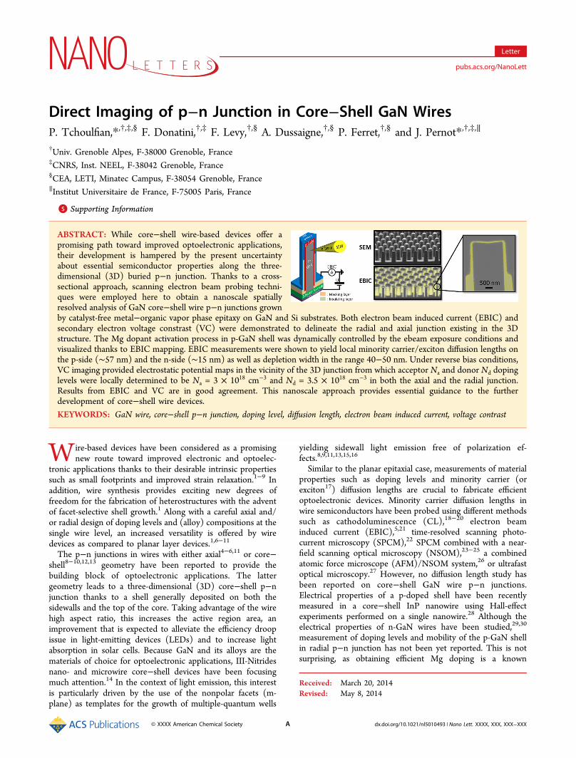
flows were used as precursors to achieve n-type and p-typedoping, respectively. Ex situ annealing to activate Mg dopantswas then performed on sample #2 while no specific annealingwas performed on sample #1. GaN wires were processed in thesame way as to fabricate a regular device. Metal contacts weredeposited on both the wires p-shell and the conductivesubstrate to allow for appropriate current injection through thesubstrate. Devices include numerous wires in parallel and noeffort to contact a single wire is required in this study. Thanksto the improved mechanical strength from the contact processsteps, it was found that a straightforward manual cleaving of asample leads statistically to numerous wires cleaved in half asdepicted in Figure 1a, which were appropriate for character-ization. This simple cross-sectional approach provided access tothe 3D buried junction and was found to be successful for GaNsusbtrates as well as for Si substrates.The sample could then be studied thanks to a FEI Inspect
F50 Schottky Field emission scanning electron microscope(FESEM) equipped with a secondary electron (SE) Everhart-Thornley detector and a homemade CL system fitted with aGATAN cryogenic stage. The wire ensemble device was biasedusing a Keythley 2611 sourcemeter. A typical I−V curve forsample #2 is reported in Figure 1e. Clear rectificationproperties were observed and the value of the turn-on voltage∼3 V was typical of a standard GaN diode behavior withappropriate ohmic contacts. Figure 1f shows the energy banddiagram of a typical p−n junction with acceptor (Na) anddonor (Nd) doping levels36 such that Na = Nd = 1018 cm−3.From the associated electric field, depletion width on both n-side and p-side can be directly inferred. For EBIC measurementof a device under bias, a lock-in technique was employed to getrid of dark current. A SR-DG535 pulse generator with typicalfrequency of 2−5 kHz allowed to synchronize a homemadeelectron beam blanker and a SR830 lock-in current amplifier inorder to extract the EBIC signal (typically 1 nA) from the
Figure 1. (a) Setup schematic of a cleaved core−shell GaN wire and its integration into a device, which allows for electron beam measurements. (b)The left-hand wire shows the structure while the two wires in the middle highlight the enhancement of the contrast of SEM images by biasing thejunction in reverse. This allows to delineate the p−n junction as well as to map the electrostatic potentials in the vicinity of the junction. The wire onthe right-hand illustrates another junction delineation procedure using EBIC signal. (c) Normalized distribution of excess carriers Δn,p in GaNinferred with CASINO v2.48 for an incident ebeam energy of 4 keV. (d) Low-temperature (10 K) spectrum acquired from an entire cleaved wirefrom sample #2. (e) I−V measurements in sample #2. (f) Energy band diagram of GaN p−n junction with Na = Nd = 1018 cm−3 at zero bias and itscorresponding electric field profile.
Nano Letters Letter
dx.doi.org/10.1021/nl5010493 | Nano Lett. XXXX, XXX, XXX−XXXB

background dark current (6 nA at −1 V, 30 nA at −2 V, and200 nA at −3 V).Figure 1b depicts schematically the SE and EBIC contrasts.
Secondary electron voltage contrast between the two sides ofthe junction dramatically increases and becomes the dominantcontrast source as the junction is reverse biased. This was usedto delineate the p−n junction and map the electrostaticpotential in its vicinity. By mapping the electric field, EBICsignal also spatially delineates the p−n junction revealing thecore−shell structure.Results from electron beam probing techniques such as
EBIC, VC, and CL not only depend on the energy bandstructure of the device under study but also on the distributionof the electron beam in the GaN material. It is thereforeessential to infer both the energy and spatial distribution of theelectron beam in order to simulate the generation of excesscarriers and draw reliable conclusions. Shown in Figure 1c isthe spatial distribution of excess carriers generated in GaNmaterial with a 4 keV ebeam as obtained by Monte Carlosimulations of electron trajectories using CASINO sofwarev2.48.37 This distribution was used to simulate the measuredEBIC signal (discussed later). We also used this simulation toinfer if the device was investigated under weak-injectionconditions (WIC), which means that the amount of excesscarriers generated by the electron beam in the sample wasnegligible with respect to the majority carrier concentration.Under high-injection conditions, the diffusion length will resultfrom both minority and majority carriers and the energy bandstructure could be modified,35 preventing any meaningfulanalysis. The procedure to calculate the excess carrierdistribution Δn, p has been previously reported in detail.5
From these calculations (detailed in Supporting Information),it was not obvious that WIC are fulfilled in p-GaN. Therefore,an experimental approach was employed by varying the ebeamcurrent and measuring the EBIC values in p-GaN. EBIC valueswere found to scale linearly with ebeam current (seeSupporting Information). We concluded that WIC weresatisfied and that the ebeam measurements under theseconditions were suitable to characterize the sample.Low-temperature CL was used to first structurally character-
ize the GaN material from sample #2. The CL signal wasproduced by the radiative recombination of the excess carriersgenerated during ebeam exposure. CL is a suitable technique toprobe nano- and microstructures, thanks to its nanometerresolution, and has been applied recently on a GaN axial p−njunction nanowire.38 A typical low-temperature (10 K) CLspectrum acquired on an entire cleaved wire with a 5 keVelectron beam and current ∼20 pA is reported in Figure 1d.Donor-bound exciton at 3.47 eV originates primarily from then-region while the dominant transition at 3.27 eV is attributedmainly to donor−acceptor pair (DAP) recombination in the p-region. The two satellites peaks are red shifted from each otherby 91 meV. This behavior is ascribed to phonon replicas withLO phonon energy in GaN equal to 91 meV.39
CL signal at 5 K has been reported to be sensitive to theelectric field existing close to a Schottky contact in ZnOnanowires and was used to measure the exciton diffusionlength.18 It is however difficult to readily apply this method onGaN p−n junction. Indeed, at 5 K the p-GaN is insulatingbecause of depth of the Mg acceptor while at room-temperatureDAP luminescence weakens dramatically as acceptors becomethermally ionized.38 Rather than CL, cross-sectional EBICmeasurements were thus employed on core−shell GaN wire p−
n junction devices in order to infer minority carrier/excitondiffusion lengths.While originally applied in microelectronics, the measure-
ment of EBIC has been very popular for the assessment ofsemiconductor junction devices as it maps the existence of anelectric field in the material, giving information on the junctionactivity and locally active defects.40 This field separateselectron−hole pairs (or possibly free excitons in GaN)generated by the ebeam leading to a current measured by acurrent amplifier. Using a cross-sectional approach, EBICmeasurement is therefore effective to localize the electric fieldregion and the active defects with a nanometer resolutionlimited by the ebeam interaction volume.Figure 2a represents a FESEM picture taken at 10 keV of a
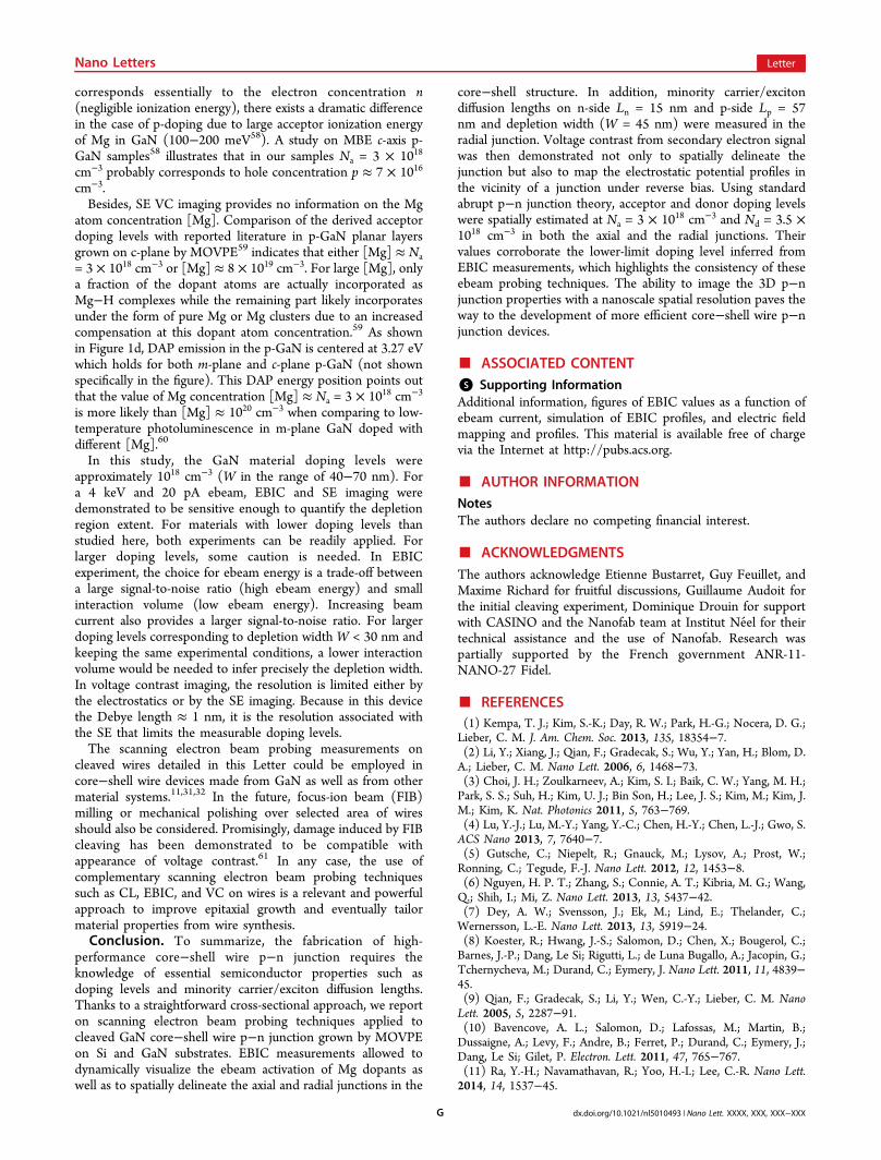
connected wire-based device from sample #1 (no ex situ
annealing) whose first-rank wires were cleaved to access theirburied junctions. The cleaving step essentially led to wirescleaved in half as schematized in Figure 1a.Figure 2b shows the corresponding EBIC map simulta-
neously acquired where the yellow color maps the current.EBIC measurement demonstrates the presence of a radialjunction even on uncleaved wires while inspection of cleavedwires also reveals the existence of an axial junction at the top ofthe wire. The knowledge of excess carrier distribution is thusessential in order to understand the charge collection. At thisangle of incidence, excess carriers generated in the top metalcontact were not reaching the p−n junction. More importantly,it demonstrates the interest of the cross-sectional approach toreadily image the p-type shell presence all around the n-typecore, as well as the p−n junction activity in core−shell wire-based devices. Such information is not accessible withoutcleaving.
Figure 2. (a) FESEM image at 10 keV of a processed wire-baseddevice along with (b) its EBIC signal (scale bar: 10 μm). First-rankwires were cleaved in half. The presence of a top junction is inferredthanks to the cleaved wires. (c) Schematic of a wire from sample #1(no p-GaN ex situ activation annealing) whose top region was exposedwith a larger ebeam dose (scale bar: 1 μm). (d) Subsequent EBICimaging shows that the latter region was ebeam activated as revealedby the localized EBIC signal obtained as a result of the improved p-doping level. (e) Electric field simulation of a core−shell p−n junctionwhere the core doping Nd = 1018 cm−3 is constant while shell doping iseither Na = 1016 cm−3 (not ebeam activated) or Na = 1018 cm−3
(ebeam activated).
Nano Letters Letter
dx.doi.org/10.1021/nl5010493 | Nano Lett. XXXX, XXX, XXX−XXXC

Figure 2b shows that the width of EBIC signal equals the p-GaN thickness (∼500 nm) in sample #1. In the case of anabrupt p−n junction, the expression of depletion width writes
ε= − ×⎡⎣⎢⎢
⎛⎝⎜
⎞⎠⎟⎤⎦⎥⎥W
V Uq N
2 ( ) 1GaN bi
eff
(1/2)
(1)
where the applied voltage is U (V), the effective doping levelNeff = (NaNd)/(Na + Nd) where Na, Nd are the acceptor anddonor doping levels, εGaN = 9ε0 is the GaN permittivity, and Vbi= [(kbT)/q] × ln[(Na × Nd)/ni
2] is the built-in potential wherekb is the Boltzmann constant, T is the absolute temperature,and ni = 1.9 × 10⁻¹⁰ cm−3 is the intrinsic carrier density in GaN.Using eq 1, p-GaN doping level in the non ex situ annealedSample #1 was estimated to be lower than Na = 2 × 1016 cm−3,taking Nd = 1018 cm−3.Figure 2c depicts a schematic where the top region defined
by the black rectangle was exposed to a larger ebeam dose ascompared to the rest of the wire. Keeping the same imagingcondition (Eb = 5 keV, Ib = 50 pA), increasing the dose totypical value of 104 μC.cm−2 (image area ≈ 4 μm2) allowed todynamically image the activation of Mg dopants over a timescale of a few seconds. In Figure 2d, EBIC mapping followingthe complete exposure of the region defined by the blackrectangle reveals that the exposed region exhibited a muchmore localized EBIC signal.The EBIC signal maps the electric field existing in the p−n
junction depletion region of width W. A larger acceptor dopinglevel results in an increase of Neff for a constant donor dopinglevel. From eq 1, it is clear that W decreases as Neff increases.The narrower EBIC signal in the exposed region thereforeevidences the ebeam induced Mg activation resulting in a largeracceptor doping level on the p-side.During MOVPE growth of Mg-doped layer, it has been
reported that interstitial hydrogen is incorporated, creating aH−Mg acceptor complex forms which passivate the accept-or.41,42 The ebeam exposure (or so-called low-electron energybeam irradiation) led to the first demonstration of p-typeconductivity in MOVPE grown GaN material,43 a keymilestone for further GaN bipolar device development.Figure 2e is a simulation using NextNano++ software44 of
the electric field in such a structure where the core doping Nd =1018 cm−3 is constant while shell doping is either Na = 1016
cm−3 (not ebeam activated) or Na = 1018 cm−3 (ebeamactivated region). The simulation does not take into accountthe diffusion of minority carriers/excitons at the proximity of
the depletion region, which contributes to the apparent EBICsignal width. The difference between the simulation and theexperiment at the border of the exposed region could thereforebe attributed to minority carrier diffusion.In this cross-sectional approach, EBIC measurement was
therefore effective to spatially delineate the p−n junction in thethree-dimensional structure. It could be used as a way to checkfor Mg dopants activation in wires grown by MOVPE and tostudy dynamically the activation process in core−shell wiredevices.Under WIC, one can infer quantitative information from
EBIC signal if a sufficient spatial resolution and signal-to-noiseratio are obtained. An EBIC profile from the radial junction in awire from sample #2 is reported in Figure 1a. Thesemiconductor properties that control the measured EBICsignal are the depletion width W (related to the doping levelsby eq 1), the minority carrier/free exciton diffusion lengths onn-side Ln and p-side Lp as well as the associated surfacerecombination velocities vn and vp.In order to determine these properties, a modified version of
Bonard and Ganiere model45 was employed where theparticular geometry in the radial junction was taken intoaccount. The degree of discrepancy between this geometry andthe usual planar-collector configuration is found to be small(discussed in Supporting Information). This model is reliable asit takes into account the spatial distribution of the generatedexcess carriers and therefore the contributions to the EBICsignal of excess carriers generated in the depletion region aswell as in the neutral n- and p-regions. This is of particularimportance in devices with depletion width in the range of theebeam interaction volume (typically for depletion width below100 nm at 4 keV).In planar p−n junctions, doping levels from both sides are
known quantities and EBIC measurements generally focus onevaluating Ln, Lp and sometimes vn and vp.
46 However, in thecase of wire devices the evaluation of depletion width is relevantto estimate the unknown doping levels. Ebeam energy hastherefore to be chosen low-enough to allow the accuratedetermination ofW. For this reason, 4 keV ebeam was found toprovide a fair spatial resolution while providing sufficient signal-to-noise level. Thanks to a previously reported technique47
based on the Monte Carlo simulation shown in Figure 1c, arealistic spatial distribution of excess carrier distribution wasimplemented in the model by using broadening parameters σx= 38 nm and σz = 12 nm in the model. Literature values forGaN surface recombination velocities are in the range v = 104
Figure 3. (a) EBIC profile in log scale of the radial junction in a wire from sample #2 under ebeam energy of 4 keV and current 20 pA. Best fit isachieved using a depletion width W = 45 nm, diffusion length on p-side Lp = 55 nm and n-side Ln = 15 nm. (b) EBIC profile of the same radialjunction as a function of applied voltage. Best fitting parameters (W, Ln, Lp) for each curve are reported in (c) where it is shown that both diffusionlengths do not depend on applied voltage whereas the depletion width increases with (Vbi − U)1/2 in agreement with abrupt junction theory. Thebest fit is obtained for W(0 V) = 45 nm corresponding to Neff ≈ 1.6 × 1018 cm−3.
Nano Letters Letter
dx.doi.org/10.1021/nl5010493 | Nano Lett. XXXX, XXX, XXX−XXXD

cm·s−1.48 Being 2 orders of magnitude lower than in GaAs,5
surface recombination was not found to play a role in the fit ofEBIC profile at 4 keV and one can therefore neglect this effectin the simulation. A previous study49 in planar devices alsoreported another EBIC modeling with negligible surfacerecombination and ascribed it to the passivation of the surfaceby the polymerization of the hydrocarbon layer producedduring the scanning of the electron beam over the surface of thesample.Fitting of the profile in Figure 1a gives W = 45 nm, Lp = 55
nm, and Ln = 15 nm. Measured diffusion lengths values are inline with reported values (Lp = 23 nm, Ln ≈ 30 nm) inliterature for cross-sectional EBIC in planar GaN p−n junctionsat low ebeam energy (1 keV)46 but larger values (Lp = 80−950nm, Ln = 70−250 nm) were reported in studies with largerebeam energies (5, 10 keV).49,50
EBIC signal was also recorded as a function of appliedvoltage U. During a single image acquisition (∼500 nm alongthe junction), reverse bias was varied by step of 1 V from 0 to−3 V. The four curves are reported in Figure 1b. Subsequentfitting gives W, Lp, and Ln for each curve. These parameterswere plotted in Figure 3c. It is seen that the diffusion lengths donot depend on the applied voltage U showing that in theneutral region, diffusion dominates over drift in this voltagerange. Interestingly,W as a function of U exhibits a (Vbi − U)1/2
variation as expected from abrupt p−n junction theory. This isillustrated by the plotted fit obtained for depletion width W(0V) = 45 nm (corresponding to Neff ≈ 1.6 × 1018 cm−3). Inabrupt junction theory, eq 1 shows that depletion width W∝[(Na + Nd)/(NaNd)]
1/2. If Na ≫ Nd (respectively Nd ≫ Na),(Na + Nd)/(NaNd)) ≈ 1/Nd (1/Na). Taking W = 45 nm, lowervalue for doping levels on each side considering thecontribution of the other side negligible are therefore Na,d =1.6 × 1018 cm−3. Although values of depletion width W weremeasured from EBIC, it is not possible to assess the exactvalues for n- and p-side doping levels without assumption. Inorder to thoroughly evaluate the doping levels, another
characterization technique needed to be employed. For thisreason, secondary electron voltage contrast measurements wereperformed.The SEM is the most widely used tool for visualization at
nanoscale. Imaging with secondary electrons highlightsprimarily topographic contrast. Over several decades, it hasbeen however consistently reported that secondary electronvoltage contrast (VC) could arise,4,51−55 particularly in p−njunction devices where the p-side appears systematicallybrighter than the n-side.4,54 The main mechanism for thiseffect is believed to be due to a difference in the escape barrierheight for secondary electrons.55 In addition, the measuredcontrast value is influenced by several experimental parameterssuch as electron dose, ebeam energy, working distance,extractor voltage, and surface treatment as previously reportedby several groups.56 Recently, VC profiles along a p−n junctionhave been demonstrated not only to map the electrostaticpotentials accross a junction with identified doping levels,54 buteven to yield the doping levels in axial GaN nanowire p−njunction where these properties were unknown.4
In this study, the configuration is the following: an Everhart−Thornley detector with 258 V grid bias, 5 mm typical workingdistance, ∼1 μm2 image dimension, and 4−5 keV and 20 pAebeam energy and current, respectively. The resolution isultimately limited either by the SE imaging or by the Debyelength. The Debye length was estimated to be 2 nm for dopinglevel in the 3 × 1018 cm−3 range,57 so that the resolution shouldbe limited by the SE imaging (and therefore below 10 nm).First, we were interested to infer whether the SE image was
really mapping the electrostatics in the vicinity of the junction.This was verified by applying a bias to the device in order tochange the band structure at the p−n junction location. Wenoticed that multiple high-magnification imaging at the samelocation resulted in contamination-induced changes in thecontrast value between n- and p-region. This prevented thecomparison with subsequent images. In order to get rid of thisissue and keep the contamination level constant, a single image
Figure 4. (a) SE image and (b) SE contrast profile of GaN wire top junction as a function of applied voltage. The contrast between the n- and p-region increases with the reverse bias. (c) Linear variation of p−n junction voltage contrast as a function of applied voltage. (d) SE contrast profileand its derivative for an applied voltage U = −2 V. Good agreement with abrupt p−n junction theory is obtained for Na = 3.0 × 1018 cm−3 and Nd =3.5 × 1018 cm−3. Total (W), n-side (Wn), and p-side (Wp) depletion widths measured in the case of (e) an axial junction and (f) a radial junction.
Nano Letters Letter
dx.doi.org/10.1021/nl5010493 | Nano Lett. XXXX, XXX, XXX−XXXE

acquisition procedure was used where the applied voltage waschanged during the imaging along the junction. It means thatthe effect of the applied voltage is inferred in a region of lengtha few hundred nanometers along the studied junction. The SEsignal S for an axial junction in a cleaved wire from sample #2 isreported in Figure 4a where the bias has been varied from −3to 2 V. The contrast C is generally defined as54
= − =−
CS S
SS S
Sref
ref
p
p (2)
where the reference signal Sref is chosen in this study to be thesignal in the neutral p-side region Sp. Figure 4b then shows thecalculated contrast C as a function of the distance along thejunction for different applied voltages U (shifted for clarity tothe same contrast level on the n-side). It can be inferred thatthe SE yield is always larger (brighter SE signal) on the p-sideas reported in the literature. A junction contrast Cpn(V) =(Sn(V) − Sp(V))/Sp(V) is defined to quantify this effect. Thedependence of Cpn on applied voltage U is reported in Figure4c where it is shown that Cpn strongly increases with the reversebias. Cpn tends toward 0 at U = Vbi. This supports the observedSE contrast as being due to the applied voltage directlydropping at the p−n junction depletion region (with negligiblevoltage drop at contacts). Surface states have been reported toplay a role in the observed VC for silicon p−n junction devices,in particular by reducing the apparent built-in voltage. In ourexperiment, the contrast observed for U = 1 V and U = 2 V arerather similar. It might reflect that contrast from surface effectsdominates from U ≈ 2 V.56 However, the large increase incontrast by reverse biasing the junction and the agreementbetween the theoretical and apparent built-in potential evidencethat the p−n junction electrostatics dominates the SE VC in thereverse bias regime. Consequently, the SE signal profile isdirectly related to the spatial distribution of electrostaticpotential across the p−n junction.Similarly to Heath et al. approach,54 the SE profile was
mapped to energy level by linearly fitting Cpn(V) = a × V + band then defining the calibrated energy as Scal = C/a where Scalwas in electronvolts. The calibrated SE signal and its spatialderivative are reported in Figure 4d for an applied bias U = −2V. Because the electric field is defined as F = 1/q × dE/dxwhere E is the energy and x is the position, the spatial derivativeof the calibrated SE signal represents a measurement of theelectric field. As illustrated in Figure 1f, the depletion width onp- and n-side could then be directly extracted from the electricfield profile. Figure 4e shows the total depletion width W, thedepletion widths on p-side Wp and n-side Wn as a function ofthe applied voltage in the same axial junction. W, Wp, and Wnexhibit a (Vbi − U)1/2 variation in agreement with abruptjunction theory. Moreover, the ratio r = Wp/Wn = Nd/Na = 1.2is constant as expected from the charge neutrality condition.Knowing r, eq 1 is finally used to fit W and yields Na = 3.0 ×1018 cm−3 and Nd = 3.5 × 1018 cm−3.The simulated curves using the derived doping levels are
compared to the calibrated SE signal Scal and its derivative inFigure 4d. A good agreement is obtained except at the bordersof the depletion region. Effect of patch fields could beresponsible for the observed difference.54
Figure 4f describes the apparent W, Wn and Wp measured fora radial junction in sample #2. A reverse bias U < −4 V wasnecessary for the SE voltage contrast to fully dominate overother contrast sources. Similar to EBIC, the particular geometry
should be taken into account for the case of a radial junction. InSupporting Information, it is shown that the geometry-inducedchange in the electric field profile in the first 10 nm below thesurface was not negligible. We accounted for this effect by usingNextNano++ simulations. In this radial junction, the estimateddoping levels are Na = 2.8 × 1018 cm−3 and Nd = 3.4 × 10¹⁸
cm−3. These values are similar to the doping levels determinedin the axial junction.A comparison between the different depletion widths (W,
Wn, Wp) in the radial and axial junction obtained from VC isplotted as a function of applied voltage in Figure 5. In this
figure, the y-axis is linear with (W)2, so that the obtained linearcharacteristics demonstrate that the abrupt junction theory isappropriate. Similar donor and acceptor doping levels areinferred in the axial and radial junctions. The depletion widthvalues for the radial (m-plane) junction estimated from VC(blue full circle symbols) are found in good agreement with thevalues derived from EBIC experiments (gray star symbols) on asimilar wire, which demonstrates the consistency of bothapproaches.In both the radial and axial junctions, we demonstrated that
the p−n junction electrostatics could be satisfactorily describedby a simple abrupt p−n junction model with constant acceptorand donor doping levels. For each junction, doping levels wereconstant over the several hundred nanometers used for thisimaging procedure. A spatially resolved evaluation of dopinglevels is possible from a single SEM picture with the deviceunder a known reverse bias chosen to increase the contrast.The ability to measure locally doping levels is an essentialindication in order to improve core−shell devices. Here, nodifference in n- and p-doping levels was found, for example, formaterial deposited on m-plane and c-plane.A recent report on secondary electron voltage contrast in
axial GaN p−n junction nanowire4 used the same approachexcept that the authors assumed to be evaluating directlyelectron and hole concentration instead of donor and acceptordoping levels. These two quantities differ because of the dopantionization energy. While the donor doping level Nd
Figure 5. Total (W), n-side (Wn) and p-side (Wp) depletion widthsobtained for m-plane (radial) and c-plane (axial) junction usingsecondary electron voltage contrast imaging as a function of appliedvoltage. Values for m-plane are estimated using a model taking intoaccount the particular geometry. The linearity between (W)2 andvoltage shows the validity of applying the abrupt junction theory.Experimental values for W derived from EBIC on m-plane is alsoplotted to show the good agreement obtained by the two techniques.
Nano Letters Letter
dx.doi.org/10.1021/nl5010493 | Nano Lett. XXXX, XXX, XXX−XXXF
corresponds essentially to the electron concentration n(negligible ionization energy), there exists a dramatic differencein the case of p-doping due to large acceptor ionization energyof Mg in GaN (100−200 meV58). A study on MBE c-axis p-GaN samples58 illustrates that in our samples Na = 3 × 10¹⁸
cm−3 probably corresponds to hole concentration p ≈ 7 × 10¹⁶
cm−3.Besides, SE VC imaging provides no information on the Mg
atom concentration [Mg]. Comparison of the derived acceptordoping levels with reported literature in p-GaN planar layersgrown on c-plane by MOVPE59 indicates that either [Mg] ≈ Na= 3 × 1018 cm−3 or [Mg] ≈ 8 × 1019 cm−3. For large [Mg], onlya fraction of the dopant atoms are actually incorporated asMg−H complexes while the remaining part likely incorporatesunder the form of pure Mg or Mg clusters due to an increasedcompensation at this dopant atom concentration.59 As shownin Figure 1d, DAP emission in the p-GaN is centered at 3.27 eVwhich holds for both m-plane and c-plane p-GaN (not shownspecifically in the figure). This DAP energy position points outthat the value of Mg concentration [Mg] ≈ Na = 3 × 1018 cm−3
is more likely than [Mg] ≈ 1020 cm−3 when comparing to low-temperature photoluminescence in m-plane GaN doped withdifferent [Mg].60
In this study, the GaN material doping levels wereapproximately 1018 cm−3 (W in the range of 40−70 nm). Fora 4 keV and 20 pA ebeam, EBIC and SE imaging weredemonstrated to be sensitive enough to quantify the depletionregion extent. For materials with lower doping levels thanstudied here, both experiments can be readily applied. Forlarger doping levels, some caution is needed. In EBICexperiment, the choice for ebeam energy is a trade-off betweena large signal-to-noise ratio (high ebeam energy) and smallinteraction volume (low ebeam energy). Increasing beamcurrent also provides a larger signal-to-noise ratio. For largerdoping levels corresponding to depletion widthW < 30 nm andkeeping the same experimental conditions, a lower interactionvolume would be needed to infer precisely the depletion width.In voltage contrast imaging, the resolution is limited either bythe electrostatics or by the SE imaging. Because in this devicethe Debye length ≈ 1 nm, it is the resolution associated withthe SE that limits the measurable doping levels.The scanning electron beam probing measurements on
cleaved wires detailed in this Letter could be employed incore−shell wire devices made from GaN as well as from othermaterial systems.11,31,32 In the future, focus-ion beam (FIB)milling or mechanical polishing over selected area of wiresshould also be considered. Promisingly, damage induced by FIBcleaving has been demonstrated to be compatible withappearance of voltage contrast.61 In any case, the use ofcomplementary scanning electron beam probing techniquessuch as CL, EBIC, and VC on wires is a relevant and powerfulapproach to improve epitaxial growth and eventually tailormaterial properties from wire synthesis.Conclusion. To summarize, the fabrication of high-
performance core−shell wire p−n junction requires theknowledge of essential semiconductor properties such asdoping levels and minority carrier/exciton diffusion lengths.Thanks to a straightforward cross-sectional approach, we reporton scanning electron beam probing techniques applied tocleaved GaN core−shell wire p−n junction grown by MOVPEon Si and GaN substrates. EBIC measurements allowed todynamically visualize the ebeam activation of Mg dopants aswell as to spatially delineate the axial and radial junctions in the
core−shell structure. In addition, minority carrier/excitondiffusion lengths on n-side Ln = 15 nm and p-side Lp = 57nm and depletion width (W = 45 nm) were measured in theradial junction. Voltage contrast from secondary electron signalwas then demonstrated not only to spatially delineate thejunction but also to map the electrostatic potential profiles inthe vicinity of a junction under reverse bias. Using standardabrupt p−n junction theory, acceptor and donor doping levelswere spatially estimated at Na = 3 × 1018 cm−3 and Nd = 3.5 ×1018 cm−3 in both the axial and the radial junctions. Theirvalues corroborate the lower-limit doping level inferred fromEBIC measurements, which highlights the consistency of theseebeam probing techniques. The ability to image the 3D p−njunction properties with a nanoscale spatial resolution paves theway to the development of more efficient core−shell wire p−njunction devices.
■ ASSOCIATED CONTENT*S Supporting InformationAdditional information, figures of EBIC values as a function ofebeam current, simulation of EBIC profiles, and electric fieldmapping and profiles. This material is available free of chargevia the Internet at http://pubs.acs.org.
■ AUTHOR INFORMATIONNotesThe authors declare no competing financial interest.
■ ACKNOWLEDGMENTSThe authors acknowledge Etienne Bustarret, Guy Feuillet, andMaxime Richard for fruitful discussions, Guillaume Audoit forthe initial cleaving experiment, Dominique Drouin for supportwith CASINO and the Nanofab team at Institut Neel for theirtechnical assistance and the use of Nanofab. Research waspartially supported by the French government ANR-11-NANO-27 Fidel.
■ REFERENCES(1) Kempa, T. J.; Kim, S.-K.; Day, R. W.; Park, H.-G.; Nocera, D. G.;Lieber, C. M. J. Am. Chem. Soc. 2013, 135, 18354−7.(2) Li, Y.; Xiang, J.; Qian, F.; Gradecak, S.; Wu, Y.; Yan, H.; Blom, D.A.; Lieber, C. M. Nano Lett. 2006, 6, 1468−73.(3) Choi, J. H.; Zoulkarneev, A.; Kim, S. I.; Baik, C. W.; Yang, M. H.;Park, S. S.; Suh, H.; Kim, U. J.; Bin Son, H.; Lee, J. S.; Kim, M.; Kim, J.M.; Kim, K. Nat. Photonics 2011, 5, 763−769.(4) Lu, Y.-J.; Lu, M.-Y.; Yang, Y.-C.; Chen, H.-Y.; Chen, L.-J.; Gwo, S.ACS Nano 2013, 7, 7640−7.(5) Gutsche, C.; Niepelt, R.; Gnauck, M.; Lysov, A.; Prost, W.;Ronning, C.; Tegude, F.-J. Nano Lett. 2012, 12, 1453−8.(6) Nguyen, H. P. T.; Zhang, S.; Connie, A. T.; Kibria, M. G.; Wang,Q.; Shih, I.; Mi, Z. Nano Lett. 2013, 13, 5437−42.(7) Dey, A. W.; Svensson, J.; Ek, M.; Lind, E.; Thelander, C.;Wernersson, L.-E. Nano Lett. 2013, 13, 5919−24.(8) Koester, R.; Hwang, J.-S.; Salomon, D.; Chen, X.; Bougerol, C.;Barnes, J.-P.; Dang, Le Si; Rigutti, L.; de Luna Bugallo, A.; Jacopin, G.;Tchernycheva, M.; Durand, C.; Eymery, J. Nano Lett. 2011, 11, 4839−45.(9) Qian, F.; Gradecak, S.; Li, Y.; Wen, C.-Y.; Lieber, C. M. NanoLett. 2005, 5, 2287−91.(10) Bavencove, A. L.; Salomon, D.; Lafossas, M.; Martin, B.;Dussaigne, A.; Levy, F.; Andre, B.; Ferret, P.; Durand, C.; Eymery, J.;Dang, Le Si; Gilet, P. Electron. Lett. 2011, 47, 765−767.(11) Ra, Y.-H.; Navamathavan, R.; Yoo, H.-I.; Lee, C.-R. Nano Lett.2014, 14, 1537−45.
Nano Letters Letter
dx.doi.org/10.1021/nl5010493 | Nano Lett. XXXX, XXX, XXX−XXXG

(12) Salomon, D.; Dussaigne, A.; Lafossas, M.; Durand, C.; Bougerol,C.; Ferret, P.; Eymery, J. Nanoscale Res. Lett. 2013, 8, 61.(13) Jacopin, G.; De Luna Bugallo, A.; Lavenus, P.; Rigutti, L.; Julien,F. H.; Zagonel, L. F.; Kociak, M.; Durand, C.; Salomon, D.; Chen, X.J.; Eymery, J.; Tchernycheva, M. Appl. Phys. Express 2012, 5, 014101.(14) Mandl, M.; Wang, X.; Schimpke, T.; Kolper, C.; Binder, M.;Ledig, J.; Waag, A.; Kong, X.; Trampert, A.; Bertram, F.; Christen, J.;Barbagini, F.; Calleja, E.; Strassburg, M. Phys. Status Solidi RRL 2013,7, 800−814.(15) Riley, J. R.; Padalkar, S.; Li, Q.; Lu, P.; Koleske, D. D.; Wierer, J.J.; Wang, G. T.; Lauhon, L. J. Nano Lett. 2013, 13, 4317−25.(16) Wang, X.; Li, S.; Mohajerani, M. S.; Ledig, J.; Wehmann, H.-H.;Mandl, M.; Strassburg, M.; Steegmuller, U.; Jahn, U.; Lahnemann, J.;Riechert, H.; Griffiths, I.; Cherns, D.; Waag, A. Cryst. Growth Des.2013, 13, 3475−3480.(17) Because of the large exciton binding energy in GaN (∼25 meV),it should be noticed that both free excitons and electron−hole pairsare stable at room temperature in GaN, so that both free exciton andminority carrier diffusion mechanisms should be considered (seeSupporting Information for a detailed discussion).(18) Hwang, J.-S.; Donatini, F.; Pernot, J.; Thierry, R.; Ferret, P.;Dang, Le Si Nanotechnology 2011, 22, 475704.(19) Gustafsson, A.; Bolinsson, J.; Skold, N.; Samuelson, L. Appl.Phys. Lett. 2010, 97, 072114.(20) Caneau, C.; Kuech, T.; Bolinsson, J.; Mergenthaler, K.;Samuelson, L.; Gustafsson, A. J. Cryst. Growth 2011, 315, 138−142.(21) Allen, J. E.; Hemesath, E. R.; Perea, D. E.; Lensch-Falk, J. L.; Li,Z. Y.; Yin, F.; Gass, M. H.; Wang, P.; Bleloch, A. L.; Palmer, R. E.;Lauhon, L. J. Nat. Nanotechnol. 2008, 3, 168−73.(22) Graham, R.; Miller, C.; Oh, E.; Yu, D. Nano Lett. 2011, 11,717−22.(23) Kelzenberg, M. D.; Turner-Evans, D. B.; Kayes, B. M.; Filler, M.a.; Putnam, M. C.; Lewis, N. S.; Atwater, H. a. Nano Lett. 2008, 8,710−4.(24) Dan, Y.; Seo, K.; Takei, K.; Meza, J. H.; Javey, A.; Crozier, K. B.Nano Lett. 2011, 11, 2527−32.(25) Gu, Y.; Romankiewicz, J. P.; David, J. K.; Lensch, J. L.; Lauhon,L. J.; Kwak, E.-S.; Odom, T. W. J. Vac. Sci. Technol., B 2006, 24, 2172.(26) Baird, L.; Ong, C. P.; Cole, R. A.; Haegel, N. M.; Talin, A. A.; Li,Q.; Wang, G. T. Appl. Phys. Lett. 2011, 98, 132104.(27) Seo, M. A.; Yoo, J.; Dayeh, S. A.; Picraux, S. T.; Taylor, A. J.;Prasankumar, R. P. Nano Lett. 2012, 12, 6334−8.(28) Storm, K.; Halvardsson, F.; Heurlin, M.; Lindgren, D.;Gustafsson, A.; Wu, P. M.; Monemar, B.; Samuelson, L. Nat.Nanotechnol. 2012, 1−5.(29) Tchoulfian, P.; Donatini, F.; Levy, F.; Amstatt, B.; Dussaigne, A.;Ferret, P.; Bustarret, E.; Pernot, J. Appl. Phys. Lett. 2013, 103, 202101.(30) Tchoulfian, P.; Donatini, F.; Levy, F.; Amstatt, B.; Ferret, P.;Pernot, J. Appl. Phys. Lett. 2013, 102, 122116.(31) Parkinson, P.; Lee, Y.-h.; Fu, L.; Breuer, S.; Tan, H. H.; Jagadish,C. Nano Lett. 2013, 13, 1405−9.(32) Howell, S. L.; Padalkar, S.; Yoon, K.; Li, Q.; Koleske, D. D.;Wierer, J. J.; Wang, G. T.; Lauhon, L. J. Nano Lett. 2013, 13, 5123−8.(33) Koester, R.; Hwang, J. S.; Durand, C.; Le Si Dang, D.; Eymery, J.Nanotechnology 2010, 21, 015602.(34) Chen, X. J.; Perillat-Merceroz, G.; Sam-Giao, D.; Durand, C.;Eymery, J. Appl. Phys. Lett. 2010, 97, 151909.(35) Nichterwitz, M.; Unold, T. J. Appl. Phys. 2013, 114, 134504.(36) The definition of acceptor Na and donor Nd doping levelsshould be understood as net doping levels taking into accountcompensation in the material. As an example in p-GaN, Na = Na
net =Na
tot − Ndcomp, where Na
tot is the concentration of dopants in theappropriate substitutional site in the lattice and Na
comp is the donorcompensation level. Same reasoning applies in n-GaN.(37) www.gel.usherbrooke.ca/casino/ (accessed Dec 1, 2013).(38) Zhou, X.; Lu, M.-Y.; Lu, Y.-J.; Gwo, S.; Gradecak, S. Appl. Phys.Lett. 2013, 102, 253104.(39) Morkov, H. Handbook of Nitride Semiconductors and Devices;Wiley-VCH Verlag GmbH & Co. KGaA: Weinheim, Germany, 2008.
(40) Vanzi, M.; Podda, S.; Musu, E.; Cao, R. Microelectron. Reliab.2013, 53, 1399−1402.(41) Nakamura, S.; Senoh, M.; Mukai, T. Jpn. J. Appl. Phys. 1991, 30,L1708−L1711.(42) Gotz, W.; Johnson, N. M.; Bour, D. P.; McCluskey, M. D.;Haller, E. E. Appl. Phys. Lett. 1996, 69, 3725.(43) Amano, H.; Kito, M.; Hiramatsu, K.; Akasaki, I. Jpn. J. Appl.Phys. 1989, 28, L2112−L2114.(44) www.nextnano.de/ (accessed Dec 1, 2013).(45) Bonard, J.-M.; Ganiere, J. J. Appl. Phys. 1996, 79, 6987−6994.(46) Moldovan, G.; Kazemian, P.; Edwards, P. R.; Ong, V. K. S.;Kurniawan, O.; Humphreys, C. J. Ultramicroscopy 107, 382−9.(47) Parish, C. M.; Russell, P. E. Appl. Phys. Lett. 2006, 89, 192108.(48) Onuma, T.; Sakai, N.; Igaki, T.; Yamaguchi, T.; Yamaguchi, A.A.; Honda, T. J. Appl. Phys. 2012, 112, 063509.(49) Gonzalez, J. C.; Bunker, K. L.; Russell, P. E. Appl. Phys. Lett.2001, 79, 1567.(50) Kumakura, K.; Makimoto, T.; Kobayashi, N.; Hashizume, T.;Fukui, T.; Hasegawa, H. Appl. Phys. Lett. 2005, 86, 052105.(51) Chee, K. W. A.; Rodenburg, C.; Humphreys, C. J. J. Phys. Conf.Ser. 2008, 126, 012033.(52) Kaestner, B.; Schonjahn, C.; Humphreys, C. J. Appl. Phys. Lett.2004, 84, 2109.(53) Li, J.; He, Y.; Han, Y.; Liu, K.; Wang, J.; Li, Q.; Fan, S.; Jiang, K.Nano Lett. 2012, 12, 4095−101.(54) Heath, J. T.; Jiang, C.-S.; Al-Jassim, M. M. J. Appl. Phys. 2012,111, 046103.(55) Sealy, C. P.; Castell, M. R.; Wilshaw, P. R. J. Electron Microsc.2000, 49, 311−321.(56) Volotsenko, I.; Molotskii, M.; Barkay, Z.; Marczewski, J.;Grabiec, P.; Jaroszewicz, B.; Meshulam, G.; Grunbaum, E.; Rosenwaks,Y. J. Appl. Phys. 2010, 107, 014510.(57) Debye length Ld = [(εGaN × kbT)/(q
2 × n)]1/2 where n is thecarrier concentration in the material.(58) Brochen, S.; Brault, J.; Chenot, S.; Dussaigne, A.; Leroux, M.;Damilano, B. Appl. Phys. Lett. 2013, 103, 032102.(59) Castiglia, A.; Carlin, J.-F.; Grandjean, N. Appl. Phys. Lett. 2011,98, 213505.(60) Monemar, B.; Paskov, P.; Pozina, G.; Hemmingsson, C.;Bergman, P.; Lindgren, D.; Samuelson, L.; Ni, X.; Morkoc, H.;Paskova, T.; Bi, Z.; Ohlsson, J. Phys. Status Solidi A 2011, 208, 1532−1534.(61) Tsurumi, D.; Hamada, K. Appl. Phys. Expr. 2013, 6, 126601.
Nano Letters Letter
dx.doi.org/10.1021/nl5010493 | Nano Lett. XXXX, XXX, XXX−XXXH