Embed Size (px)
Citation preview

ECE 335: Electronic Engineering
Lecture 8:
Bipolar Junction Transistors (BJTs)
Faculty of EngineeringFaculty of EngineeringFaculty of EngineeringFaculty of Engineering

Agenda
• History
• Basic Understanding
• Practical Aspects
• Structure & Symbol
• Basic Operation
• BJT Amplifier Basics
• Common Emitter Charcateristics

HISTORY

The transistor was probably
the most important invention
of the 20th Century, and the
story behind the invention is
one of clashing egos and top
secret research.
First - BJTs
Reference:
Bell Labs Museum
B. G. Streetman & S. Banerjee ‘Solid State Electronic Devices’, Prentice Hall 1999.

Picture shows the workbench of John
Bardeen (Stocker Professor at OU) and Walter
Brattain at Bell Laboratories. They were supposed to
be doing fundamental research about crystal surfaces.
The experimental results hadn't been very
good, though, and there's a rumor that their boss,
William Shockley, came near to canceling the
project. But in 1947, working alone, they switched to
using tremendously pure materials.
It dawned on them that they could build the
circuit in the picture. It was a working
amplifier! John and Walter submitted a patent for the
first working point contact transistor.
Interesting story…

Shockley was furious and took their work
and invented the junction transistor and submitted
a patent for it 9 days later.
The three shared a Nobel Prize in 1955. Bardeen
and Brattain continued in research (and Bardeen
later won another Nobel).
Shockley quit to start a semiconductor
company in Palo Alto. It folded, but its staff went
on to invent the integrated circuit (the "chip") and
to found Intel Corporation.
By 1960, all important computers used transistors
for logic, and ferrite cores for memory.
Interesting story…
BASIC UNDERSTANDING

Bipolar Junction Transistors
(BJTs)• The bipolar junction transistor is a semiconductor
device constructed with three doped regions.
• These regions essentially form two ‘back-to-back’
p-n junctions in the same block of semiconductor
material (silicon).
• The most common use of the BJT is in linear
amplifier circuits (linear means that the output is
proportional to input). It can also be used as a
switch (in, for example, logic circuits).

Understanding of BJT

Basic models of BJT
Diode
Diode
Diode
Diode
npn transistor
pnp transistor

Basic models of BJT

PRACTICAL ASPECTS

BJTs – Practical Aspects
Heat sink

BJTs – Testing

BJTs – Testing

BJT STRUCTURE AND
SYMBOL

npn-BJT Structure
• The ‘npn’ version of the BJT consists of
two n regions separated by a p region (as
the name suggests). A schematic of an npn
transistor is shown.
n-type p-type n-type

BJT Structure
• The three regions are known as the emitter,
base and collector regions.
• Electrical connections are made to each of
these regions.

npn-BJT Structure
E
Emitter
(n-type)
Base
(p-type)Collector
(n-type)
B
C

npn BJT Symbol

npn BJT Symbol
E
B
C

pnp BJT Symbol
• In the symbol for a pnp BJT transistor the
direction of the arrow on the emitter is
reversed
E
B
C

BJT Circuits
• Most electronic devices take the signal between
two input terminals and deliver from it an output
signal between two output terminals.
• The BJT has only three terminals so one of these
is usually shared (i.e. made common) between
input and output circuits.
• We thus talk about common emitter (CE),
common base (CB) and common collector (CC)
configurations.

BJT Circuits
• The CE configuration is the one most commonly
encountered since it provides both good current
and voltage gain for ac signals.
• In the CE configuration the input is between the
base and the emitter. The output is between the
collector and the emitter.
• All three configurations will be dealt with next
semester

Current Directions (Convention)
• We define currents directions such that the collector current (IC) and base current (IB) flow into the device whereas the emitter current (IE) flows out of the device.
• THIS IS IMPORTANT; we shall shortly treat the transistor as a current node and write
IC + IB = IE (Kirchhoff)

Current Flow Convention
EEmitter
(n-type)
Base
(p-type)Collector
(n-type)
B
C
IE
IB
IC
W << Ldiff

npn BJT Structure
• The emitter (E) and is heavily doped (n-type).
• The collector (C) is also doped n-type.
• The base (B) is lightly doped with opposite type to the emitter and collector (i.e. p-type in the npn transistor).
• The base is physically very thin for reasons described below. (W << Ldiff)
B-E and C-B Junctions
• The p-n junction joining the base and emitter regions is called the base-emitter (B-E) junction. (or emitter-base, it doesn’t really matter)
• The p-n junction between the base and collector regions is called the collector-base (C-B) junction.(or base-collector)

BASIC OPERATION

(Very) Basic Operation
• In normal operation for analogue (linear amplifier) circuits the emitter-base junction is forward biasedand the collector-base junction is reverse biased.
• These ‘bias’ or ‘quiescent’ conditions are set by d.c. bias circuits.
• The a.c. (‘analogue’) signal to be amplified is superimposed on top of the d.c. bias voltages and currents. (Exactly as for dynamic resistance, small variations about a Q point, in our discussion of diodes.)

BJT Operation
• The forward bias between the base and
emitter injects electrons from the emitter
into the base and holes from the base into
the emitter.
EE
(n)
B
(p) C
(n)B
C

BJT Operation
• The forward bias between the base and emitter
injects electrons from the emitter into the base and
holes from the base into the emitter.
• As the emitter is heavily doped and the base
lightly doped most of the current transport across
this junction is due to the electrons flowing from
emitter to base.

BJT Operation
• The base is lightly doped and physically
very thin.
• Thus only a small percentage of electrons
flowing across the base-emitter (BE)
junction combine with the available holes in
this region.

BJT Operation
• Most of the electrons (a fraction α which is close
to 1, e.g. 0.98) flowing from the emitter into the
base reach the collector-base (CB) junction.
• Once they reach this junction they are ‘pulled’
across the reverse biased CB junction into the
collector region i.e. they are collected.
• Those electrons that do recombine in the base give
rise to the small base current IB.

BJT Operation
• The electrons ‘collected’ by the collector at the C-B junction essentially form the collector current inthe external circuit.
• There will also be a small contribution to collectorcurrent, called ICO, from the reverse saturationcurrent across the CB junction.
• The base current supplies positive charge toneutralise the (relatively few) electronsrecombining in the base. This prevents the buildup of charge which would hinder current flow.

BJT Operation.
The Critical Knowledge!
• The (relatively large) collector current is
directly controlled by the (much smaller)
base current.
• This is further illustrated and clarified in
the following discussions of the BJT’s
current-voltage characteristics.
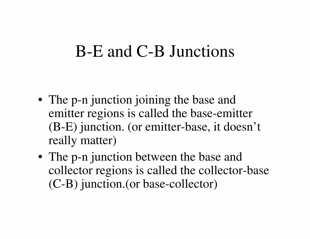
BJT Transistor Man (after
Horowitz and Hill)
βIBForward biased diode


![Chapter 4 Introduction to Bipolar Junction Transistors (BJTs)...Introduction to Bipolar Junction Transistors (BJTs) 4.1 Introduction [5] The transistor was invented by a team of three](https://img.dokumen.tips/doc/110x75/5f73167be644cf1b4d346cf2/chapter-4-introduction-to-bipolar-junction-transistors-bjts-introduction-to.jpg)