Embed Size (px)
Citation preview

1
University of missan
Electrical Engineering Department
Electronic II, Second year
2015-2016
Part ILectures
Bipolar Junction Transistors(BJTs) and Circuits
Assistant Lecture: Maab Alaa Hussain

2
University of Missan Bipolar Junction Transistors Electrical Engineering Department Second Year, Electronics I I, 2015 - 2016 Maab Alaa Hussain
Bipolar Junction Transistors (BJTs)
Basic Construction: The transistor is a three-layer semiconductor device consisting of either two n- and one
p-type layers of material or two p- and one n-type layers of material. The former is
called an npn transistor, while the latter is called a pnp transistor. Both (with symbols)
are shown in Fig. 1 -1. The middle region of each transistor type is called the base (B)
of the transistor. Of the remaining two regions, one is called emitter (E) and the other is
called the collector (C) of the transistor. For each transistor type, a junction is created at
each of the two boundaries where the material changes from one type to the other.
Therefore, there are two junctions: emitter-base (E-B) junction and collector-base
(C-B) junction. The outer layers of the transistor are heavily doped semiconductor
materials having widths much greater than those of the sandwiched p- or n-type
material. The doping of the sandwiched layer is also considerably less than that of the
outer layers (typically 10:1 or less). This lower doping level decreases the conductivity
(increases the resistance) of this material by limiting the number of "free" carriers.
E
n p n
C
E
p n
p
C
(Emitter)
E-B junction
B (Base)
(Collector)
C-B junction
B
E
B
C
Fig. 1-1
E
B
C
The dc biasing is necessary to establish the proper region of operation for ac
amplification or switching purposes. Table 8-1 shows the transistor operation regions
and the purpose with respect to the biasing of the E-B and C-B junctions.
Table 8-1
The abbreviation BJT, from bipolar junction transistor, is often applied to this
three-terminal device. The term bipolar reflects the fact that holes and electrons
participate in the injection process into the oppositely polarized material. If only one
carrier is employed (electron or hole), it is considered a unipolar device. Such a device
is the field-effect transistor (FET).
Operation region Purpose Junctions biasing
E-B junction bias C-B junction bias
1 Active region Amplification Forward-biased Reverse-biased
2 Cutoff region Switching
Reverse-biased Reverse-biased
3 Saturation region Forward-biased Forward-biased

3
University of Misszn Bipolar Junction Transistors Electrical Engineering Department Second Year, Electronics I I, 2015 - 2016 Maab Alaa Hussain
Active Region Operation:
The basic operation of the transistor will now be described using the pnp transistor of
Fig. 1-2. The operation of the npn transistor is exactly the same if the roles played by
the electron and hole are interchanged. When the E-B junction is forward-biased, a
large number of majority carriers will diffuse across the forward-biased p-n junction
into the n-type material (base). Since the base is very thin and has a low conductivity
(lightly doping), a very small number of these carriers will take this path of high
resistance to the base terminal. The larger number of these majority carriers will diffuse
across the reverse-biased C-B junction into the p-type material (collector). The reason
for the relative ease with which the majority carriers can cross the reverse-biased
C-B junction is easily understood if we consider that for the reverse-biased diode the
injected majority carriers will appear as minority carriers in the n-type base region
material. Combining this with the fact that all the minority carriers in the depletion
region will cross the reverse-biased junction of a diode accounts for the flow indicated
in Fig. 1-2.
Fig. 1-2
Applying Kirchhoff's current law to the transistor of Fig. 1-2, we obtain
I E IC I B
[1.1]
The collector current, however, is comprised of two components: the majority and
minority carriers as indicated in Fig. 1-2. The minority-current component is called the
leakage current and is given the symbol ICO (IC current with emitter terminal Open).
The collector current, therefore, is determined in total by Eq. [1.2].
I C = IC majority + ICO minority
[1.2]

4
University of Missan Bipolar Junction Transistors Electrical Engineering Department Second Year, Electronics I I, 2015 - 2016 Maab Alaa Hussain
Common-Base (CB) Configuration:
The common-base configuration with npn and pnp transistors are indicated in Fig. 1-3.
The common-base terminology is derived from the fact that the base is common to both
input and output sides of the configuration. In addition, the base is usually terminal
closest to, or at, the ground potential.
I E
E
C
IC
I E
E
C IC
VEE
VBE
B
I B
VCB
VCC
VEE
VEB
B
I B
VBC
VCC
Fig. 1-3
In the dc mode the levels of IC and IE due to the majority carriers are related by a
quantity called alpha (αdc) and defined by the following equation:
dc
IC
I E
[1.3]
Where IC and IE are the levels of current at the point of operation and αdc ≈ 1, or for
practical devices: 0.900 ≤ αdc ≤ 0.998.
Since alpha is defined solely for the majority
carriers and from Fig. 1-4, Eq. [1.2] becomes
IC I E ICBO
[1.4]
Fig. 1-4
The input (emitter) characteristics for a CB
configuration are a plot of the emitter (input)
current (IE) versus the base-to-emitter (input)
voltage (VBE) for a rage of values of the collector-
to-base (output) voltage (VCB) as shown in Fig. 1-5.
Since, the exact shape of this IE-VBE carve will
depend on the reverse-biasing output voltage, VCB.
The reason for this dependency is that the grater the
value of VCB, the more readily minority carriers in
the base are swept through the C-B junction. The
increase in emitter-to-collector current resulting
from an increase in VCB means the emitter current
will be greater for a given value of base-to-emitter
voltage (VBE).
Fig. 1-5

5
University of Missan Bipolar Junction Transistors Electrical Engineering Department Second Year, Electronics I I, 2015 - 2016 Maab Alaa Hussain
The output (collector) characteristics for
CB configuration will be a plot of the collector
(output) current (IC) versus collector-to-base
(output) voltage (VCB) for a range of values of
emitter (input) current (IE) as shown in Fig. 1-6.
The collector characteristics have three basic
region of interest, as indicated in Fig. 1-6, the
active, cutoff, and saturation regions.
Active region:
VCB > 0 and IC I E . Cutoff region:
IE = 0 and IC ICBO .
Saturation region: Fig. 1-6
VCB < 0 and IC(sat.) I E(sat.) .
For ac situations where the point of operation moves on the characteristic carve,
an ac alpha (αac) is defined by
ac
IC
I E
VCB const.
[1.5]
The ac alpha is formally called the common-base, short-circuit, amplification factor,
and for most situations the magnitudes of αac and αdc are quite close, permitting the use
of the magnitude of one for other.
Fig. 1-7 shows how the common-base
output characteristics appear when the
effects of breakdown are included. Note the
sudden upward swing of each curve at a
large value of VCB. The collector-to-base
breakdown voltage when IE = 0 (emitter
open) is designed BVCBO.
Fig. 1-7
Transistor Amplification Action:
The basic voltage-amplifying action of the CB configuration can now be described
using the circuit of Fig. 1-8. The dc biasing does not appear in the figure since our
interest will be limited to the ac response. For the CB configuration, the input resistance
between the emitter and the base of a transistor will typically vary from 10 to 100 Ω, while the output resistance may vary from 100 kΩ to 1 MΩ. The difference in
resistance is due to the forward-biased junction at the input (base to emitter) and the
reverse-biased junction at the output (base to collector). Using effective values and a
common value of 20 Ω for the input resistance, we find that
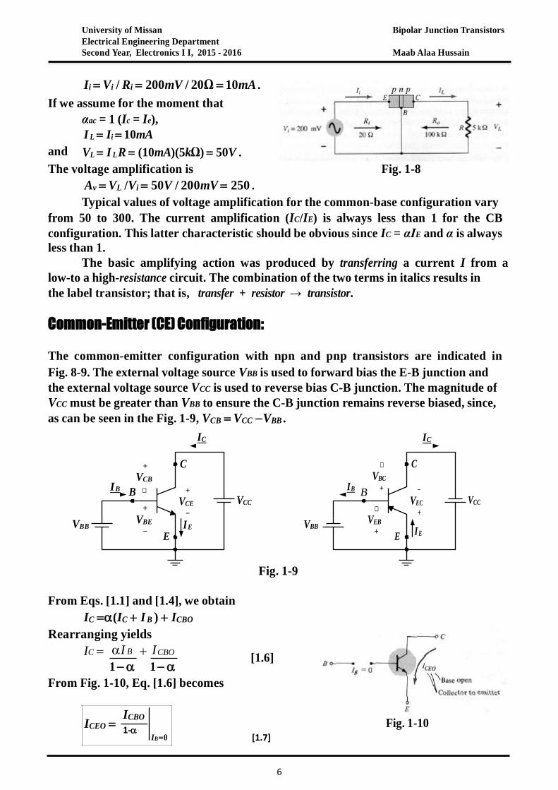
6
B
I B I
University of Missan Bipolar Junction Transistors Electrical Engineering Department Second Year, Electronics I I, 2015 - 2016 Maab Alaa Hussain
Ii Vi / Ri 200mV / 20Ω 10mA .
If we assume for the moment that
and
αac = 1 (Ic = Ie),
I L Ii 10mA
VL I L R (10mA)(5kΩ) 50V .
The voltage amplification is Fig. 1-8
Av VL /Vi 50V / 200mV 250 .
Typical values of voltage amplification for the common-base configuration vary
from 50 to 300. The current amplification (IC/IE) is always less than 1 for the CB
configuration. This latter characteristic should be obvious since IC = αIE and α is always
less than 1.
The basic amplifying action was produced by transferring a current I from a
low-to a high-resistance circuit. The combination of the two terms in italics results in
the label transistor; that is, transfer + resistor → transistor.
Common-Emitter (CE) Configuration:
The common-emitter configuration with npn and pnp transistors are indicated in
Fig. 8-9. The external voltage source VBB is used to forward bias the E-B junction and
the external voltage source VCC is used to reverse bias C-B junction. The magnitude of
VCC must be greater than VBB to ensure the C-B junction remains reverse biased, since,
as can be seen in the Fig. 1-9, VCB VCC VBB .
IC IC
VBB
I B
VCB
B
VBE
E
C
VCE
I E
VCC
VBB
I B
VBC
VEB
E
C
VEC
I E
VCC
Fig. 1-9
From Eqs. [1.1] and [1.4], we obtain
IC (IC I B ) ICBO
Rearranging yields
1 1
From Fig. 1-10, Eq. [1.6] becomes
[1.6]
ICEO
ICBO
1-
IB 0 [1.7]
Fig. 1-10
IC CBO

7
University of Missan Bipolar Junction Transistors Electrical Engineering Department Second Year, Electronics I I, 2015 - 2016 Maab Alaa Hussain
In the dc mode the levels of IC and IB are related by a quantity called beta (βdc)
and defined by the following equation:
βdc
IC
I B
[1.8]
Where IC and IB are the levels of current at the point of operation. For practical devices
the levels of βdc typically ranges from about 50 to over 500, with most in the mid range.
On specification sheets βdc is usually included as hFE with h derived from an ac hybrid
equivalent circuit.
For ac situation an ac beta (βac) has been defined as follows:
β ac
IC
I B
VCE const.
[1.9]
The formal name for βac is common-emitter, forward-current, amplification factor
and on specification sheets βac is usually included as hfe.
A relationship can be developed between β and α using the basic relationships
introduced thus far. Using β IC / I B we have I B IC / β , and from IC / I E
we have I E IC / . Substituting into I E IC I B we have IC / IC IC / β and
dividing both sides of the equation by IC will result in 1/ 1 1/ β or
β β (β 1) so that
Β
β 1
or β
1
[1.10]
In addition, recall that ICEO ICBO /(1 ) but using an equivalence of
1/(1 ) β 1 derived from the above, we find that ICEO (β 1)ICBO or
ICEO βICBO
[1.11]
Beta is particularly important parameter because it provides a direct link between
current levels of the input and output circuits for CE configuration. That is,
IC βI B ICEO βI B
[1.12]
and since I E IC I B βI B I B we have
I E (β 1)I B
[1.13]

8
University of Missan Bipolar Junction Transistors Electrical Engineering Department Second Year, Electronics I I, 2015 - 2016 Maab Alaa Hussain
The input (base) characteristics for the CE configuration are a plot of the base
(input) current (IB) versus the base-to-emitter (input) voltage (VBE) for a range of values
of collector-to-emitter (output) voltage (VCE) as shown in Fig. 1-11. Note that IB
increases as VCE decreases, for a fixed value of VBE. A large value of VCE results in a
large reverse bias of the C-B junction, which widens the depletion region and makes the
base smaller. When the base is smaller, there are fewer recombinations of injected
minority carriers and there is a corresponding reduction in base current (IB).
Fig. 1-11 Fig. 1-12
The output (collector) characteristics for CE configuration are a plot of the
collector (output) current (IC) versus collector-to-emitter (output) voltage (VCE) for a
range of values of base (input) current (IB) as shown in Fig. 1-12. The collector
characteristics have three basic region of interest, as indicated in Fig. 1-12, the active,
cutoff, and saturation regions.
Active region: IB > 0 and IC βI B .
Cutoff region: IB = 0 and IC ICEO .
Saturation region: VCE ≈ 0 and I B(sat.) IC(sat.) / β .
Common-Collector (CC) Configuration:
The third and final transistor configuration is the common-collector configuration,
shown in Fig. 1-13 with npn and pnp transistors. The CC configuration is used
primarily for impedance-matching purposes since it has a high input impedance and
low output impedance, opposite to that which is true of the common-base and
common-emitter configurations.
From a design viewpoint, there is no need for a set of common-collector
characteristics to choose the circuit parameters. The circuit can be designed using the
common-emitter characteristics. For all practical purposes, the output characteristics
of the CC configuration are the same as for the CE configuration. For the CC
configuration the output characteristics are a plot of emitter (output) current (IE)
versus collector-to-emitter (output) voltage (VCE), for a range of values of base (input)

9
B B
University of Missan Bipolar Junction Transistors Electrical Engineering Department Second Year, Electronics I I, 2015 - 2016 Maab Alaa Hussain
current (IB). The output current, therefore, is the same for both the common-emitter
and common-collector characteristics. There is an almost unnoticeable change in the
vertical scale of IC of the common-emitter characteristics if IC is replaced by IE for the
common-collector characteristics (since 1, I E IC ).
I E I E
VBB
I B
VBE
VCB
C
E
VCE
IC
VCC
VBB
I B
VEB
VBC
C
E
VEC
IC
VCC
Fig. 1-13
Transistor Casing and Terminal Identification:
Whenever possible, the transistor casing will have some marking to indicate which
leads are connected to the emitter, collector, or base of a transistor. A few of the
methods commonly used are indicated in Fig. 1-14.
Fig. 1-14
Exercises:
1. Given an αdc of 0.998, determine IC if IE = 4 mA.
2. Determine αdc if IE = 2.8 mA and IB = 20 µA.
3. Find IE if IB = 40 µA and αdc is 0.98.
4. Given that αdc = 0.987, determine the corresponding value of β.
5. Given βdc = 120, determine the corresponding value of α.
6. Given that βdc = 180 and IC = 2.0 mA, find IE and IB.
7. A transistor has ICBO = 48 nA and α = 0.992.
i. Find β and ICEO.
ii. Find its (exact) collector current (IC) when IB = 30 μA.
iii. Find the approximate collector current, neglecting leakage current.

10
University of Missan DC Biasing Circits of BJTs Electrical Engineering Department Second Year, Electronics I I, 2015 - 2016 Maab Alaa Hussain
DC Biasing Circuits of BJTs
Basic Concepts: The analysis or design of a transistor amplifier requires a knowledge of both the dc and
ac response of the system. Too often it is assumed that the transistor is a magical device
that can raise the level of the applied ac input without the assistance of an external
energy source. In actuality, the improved output ac power level is the result of a
transfer of energy from the applied dc supplies. The analysis or design of any electronic
amplifier therefore has two components: the dc portion and the ac portion. Fortunately,
the superposition theorem is applicable and the investigation of the dc conditions can
be totally separated from the ac response. However, one must keep in mind that during
the design or synthesis stage the choice of parameters for the required dc levels will
affect the ac response, and vice versa.
The term biasing appearing in the title of this lecture is an all-inclusive term for
the application of dc voltages to establish a fixed level of current and voltage. For
transistor amplifiers the resulting dc current and voltage establish an operating point on
the characteristics that define the region that will be employed for amplification of the
applied signal. Since the operating point is a fixed point on the characteristics, it is also
called the quiescent point (abbreviated Q-point). By definition, quiescent means quiet,
still, inactive. Fig. 2-1 shows a general output device characteristic with four operating
points indicated. The biasing circuit can be designed to set the device operation at any
of these points or others within the active region. The maximum ratings are indicated
on the characteristics of Fig. 2-1 by a horizontal line for the maximum collector current
ICmax and a vertical line at the maximum collector-to-emitter voltage VCEmax. The
maximum power constraint is defined by the curve PCmax in the same figure. At the
lower end of the scales are the cutoff region, defined by IB ≤ 0 μA, and the saturation
region, defined by VCE ≤ VCE(sat).
Fig. 2-1

11
I B CC
IC CC
VCEQ VCC
ICQ IC (sat) CC
University of Missan DC Biasing Circits of BJTs Electrical Engineering Department Second Year, Electronics I I, 2015 - 2016 Maab Alaa Hussain
Standard Biasing Circuits:
1. Fixed-Bias Circuit:
Fig. 2-2a shows a fixed-bias circuit.
Analysis:
- For the input (base-emitter circuit) loop
as shown in Fig. 2-2b:
VCC I B RB VBE 0
V VBE
RB
[2.1a]
- For the output (collector-emitter circuit) (a)
loop as shown in Fig. 2-2c:
IC βI B
VCE IC RC VCC 0
VCE VCC IC RC
[2.1b]
- For the transistor terminal voltages:
VE 0V
VB VCC I B RB VBE
VC VCC I C RC VCE
[2.1c]
(b) (c)
Load-Line Analysis:
From Eq. [2.1b] and Fig. 2-3: Fig. 2-2
At cutoff region:
VCE VCC IC 0
At saturation region:
[2.2a]
V
RC VCE 0
Design:
For an optimum design:
1
2
1 V
2 2RC
[2.2b]
[2-3]
ICQ
Fig. 2-3
VCEQ

12
VCEQ VCC
ICQ IC (sat)
University of Missan DC Biasing Circits of BJTs Electrical Engineering Department Second Year, Electronics I I, 2015 - 2016 Maab Alaa Hussain
2. Emitter-Stabilized Bias Circuit:
Fig. 2-4a shows an emitter-stabilized bias circuit.
Analysis:
For the input (base-emitter circuit) loop
as shown in Fig. 2-4b:
VCC I B RB VBE I E RE 0
I E (β 1)I B
I B VCC VBE
RB (β 1)RE
[2.4a]
For the output (collector-emitter circuit) (a)
loop as shown in Fig. 2-4c:
I E RE VCE IC RC VCC 0
I E IC
VCE VCC IC (RC RE )
[2.4b]
For the transistor terminal voltages:
VE I E RE
VB VCC I B RB VE VBE
VC VCC IC RC VE VCE
[2.4c]
(b) (c)
Load-Line Analysis:
From Eq. [2.4b] and Fig. 2-5: Fig. 2-4
At cutoff region:
VCE VCC IC 0
At saturation region:
[2.5a]
IC
Design:
VCC
RC RE VCE 0
[2.5b]
ICQ
For an optimum design:
1
2
1 VCC
2 2(RC RE )
VCEQ
[2-6] Fig. 2-5
VE 1
10
VCC

13
I B
VB [2.8a] (d)
IC E E I
University of Missan DC Biasing Circits of BJTs Electrical Engineering Department Second Year, Electronics I I, 2015 - 2016 Maab Alaa Hussain
3. Voltage-Divider Bias Circuit:
Fig. 2-6a shows a voltage-divider bias circuit.
Analyses:
For the input (base-emitter circuit) loop:
Exact Analysis:
From Fig. 2-6b:
RTh R1 R2
From Fig. 2-6c:
[2.7a]
Eth=VR2= R2VCC
R1 R2
[2.7b]
From Fig. 2-6d: (a)
ETh I B RTh VBE I E RE 0
I E (β 1)I B
ETh VBE
RTh (β 1)RE
IC I B
[2.7c]
Approximate Analysis: (b) (c)
From Fig. 2-6e:
If Ri R2 => I 2 I B .
Since I B 0 => I1 I 2 .
Thus R1 in series with R2.
That is,
R2VCC
R1 R2
Since Ri (β 1)RE βRE the condition
that will define whether the approximation
approach can be applied will be the
following:
βRE ≥ 10R2
and
VE VB VBE
V
RE
[2.8b]
[2.8c] (e)
For the output (collector-emitter circuit) loop: Fig. 2-6
VCE VCC IC (RC RE ) [2.9]

14
VCEQ VCC
ETh R2VCC (3.9k )(22)
I B
6.05µA
VB R2VCC (3.9k )(22)
ICQ E 0.867mA VE 1.3
University of Missan DC Biasing Circits of BJTs Electrical Engineering Department Second Year, Electronics I I, 2015 - 2016 Maab Alaa Hussain
Load-Line Analysis:
The similarities with the output circuit of the emitter-biased configuration result in the
same intersections for the load line of the voltage-divider configuration. The load line
will therefore have the same appearance as that of Fig. 2-5. The level of IB is of course
determined by a different equation for the voltage-divider bias and the emitter-bias
configuration.
Design:
For an optimum design:
1
2
1 Ic(sat) = VCC
2 2(RC RE )
𝑽𝑬 = 𝟏/𝟏𝟎 𝑽𝒄𝒄
102 R β RE
[2.10]
Example 2-1:
Determine the dc bias voltage VCE and the current IC for the voltage-divider
configuration of Fig. 2-6a with the following parameters: VCC = +22 V, β = 140,
R1 = 39 kΩ, R2 = 3.9 kΩ, RC = 10 kΩ, and RE = 1.5 kΩ.
Solution:
Exact:
RTh R1 R2 39k 3.9k 3.55Ω
2V R1 R2 39k 3.9k
ETh VBE
RTh (β 1)RE
2 - 0.7
3.55k (141)(1.5k )
I CQ β I B (140)(6.05µ ) 0.85mA
VCEQ VCC IC (RC RE )
22 (0.85m)(10k 1.5k )
12.23V
Approximate:
Testing: β RE ≥10R2
(140)(1.5k ) ≥ 10(3.9k )
210kΩ 39kΩ(satisfied)
2V
R1 R2 39k 3.9k
VE VB VBE 2 0.7 1.3V
I
RE 1.5k
VCEQ VCC IC (RC RE )
22 (0.867m)(10k 1.5k )
12.03V

15
VCEQ VCC
IC (sat)
University of Missan DC Biasing Circits of BJTs Electrical Engineering Department Second Year, Electronics I I, 2015 - 2016 Maab Alaa Hussain
4. Voltage-Feedback Bias Circuit:
Fig. 2-7a shows a voltage-feedback bias circuit.
Analysis:
For the input (base-emitter circuit) loop
as shown in Fig. 2-7b:
VCC IC RC I B RB VBE I E RE 0
IC IC I B I EIC β I B
VCC β I B RC I B RB VBE β I B RE 0
I B VCC VBE
RB β (RC RE )
[2.11a]
For the output (collector-emitter circuit) (a)
loop as shown in Fig. 2-7c:
I E RE VCE IC' RC VCC 0
IC' I E IC
VCE VCC IC (RC RE )
[2.11b]
Load-Line Analysis:
Continuing with the approximation IC IC will result
in the same load line defined for the voltage-divider and
emitter-biased configurations. The levels of IBQ will be
defined by the chosen base configuration.
(b)
Design:For an optimum design:
1
2
ICQ 1 VCC
2 2(RC RE )
[2-12]
VE 1
10
VCC
RB ≤ β (RC RE )
(c)
Fig. 2-7
Ic'
Ic'
Ic'
Ic(sat)=

16
I B EE BE V 83µA
V VEE 20 20
I B EE Th BE
University of Missan DC Biasing Circits of BJTs Electrical Engineering Department Second Year, Electronics I I, 2015 - 2016 Maab Alaa Hussain
Other Biasing Circuits:
Example 2-2: (Negative Supply)
Determine VC and VB for the circuit of Fig. 2-8.
Solution:
I B RB VBE VEE 0 (KVL)
V - V 9 0. 7
RB 100k
IC β I B (45)(83µ ) 3.735mA
VC I C RC (3.735m)(1.2k ) 4.48V
VB I B RB (83µ )(100k ) 8.3V
Example 2-3: (Two Supplies)
Determine VC and VB for the circuit of Fig. 2-9a.
Solution:
From Fig. 2-9b:
RTh R1 R2 8.2k 2.2k 1.73kΩ
I CC 3.85mA R1 R2 8.2k 2.2k
ETh IR2 VEE (3.85m)(2.2k ) 20 11.53V
Fig. 2-8
(a)
From Fig. 2-9c:
ETh I B RTh VBE I E RE VEE 0
I E (β 1)I B
V E V
RTh (β 1)RE
(KVL)
(b)
20 11.53 0.7
1.73k (121)(1.8k ) 35.39µA
IC β I B (120)(35.39µ ) 4.25mA
VC VCC IC RC 20 (4.25m)(2.7k ) 8.53V
VB ETh I B RTh (11.53) (35.39µ )(1.73k )
11.59V
(c)
Fig. 2-9
=k100
7.09.0

17
V VBE 4 0.7
I B 45.8µA
I B
University of Missan DC Biasing Circits of BJTs Electrical Engineering Department Second Year, Electronics I I, 2015 - 2016 Maab Alaa Hussain
Example 2-4: (Common-Base)
Determine VCB and IB for the common-base configuration of Fig. 2-10.
Solution:
Applying KVL to the input circuit:
VEE I E RE VBE 0
I E EE 2.75mA
RE 1.2k
Applying KVL to the output circuit:
VCB I C RC VCC 0
VCB VCC IC RC
with IC I E
VCB 10 (2.75m)(2.4k ) 3.4V
Fig. 2-10
IC 2 .75m
β 60
Example 2-5: (Common-Collector)
Determine IE and VCE for the common-collector (emitter-follower) configuration of
Fig. 2-11.
Solution:
Applying KVL to the input circuit:
I B RB VBE I E RE VEE 0
I E (β 1)I B
VEE VBE
RB (β 1)RE
20 0.7
240k (91)(2k ) 45.73µA
I E (β 1)I B (91)(45.73µ ) 4.16mA
Applying KVL to the output circuit:
VEE I E RE VCE 0
VCE VEE I E RE 20 (4.16m)(2k ) 11.68V
Fig. 2-11
-
-

18
VB 3.16V
IC E 2.24mA VE 2.46
University of Missan DC Biasing Circits of BJTs Electrical Engineering Department Second Year, Electronics I I, 2015 - 2016 Maab Alaa Hussain
Example 2-6: (PNP Transistor)
Determine VCE for the voltage-divider bias configuration of Fig. 2-12.
Solution:
Testing: β RE ≥ 10R2
(120)(1.1k ) ≥ 10(10k )
132kΩ ≥100kΩ(satisfied )
R2VCC (10k )(18)
R1 R2 47k 10k
VE VB VBE 3.16 (0.7) 2.46V
I
RE 1.1k
I E RE VCE IC RC VCC 0 (KVL)
VCE VCC IC (RC RE )
18 (2.24m)(2.4k 1.1k ) 10.16V
Fig. 2-12
Exercises:
1. For the fixed-biased configuration of Fig. 2-2a with the following parameters:
VCC = +12 V, β = 50, RB = 240 kΩ, and RC = 2.2 kΩ, determine:
IBQ, ICQ, VCEQ, VB, VC, and VBC.
2. Given the device characteristics of Fig. 2-13a, determine VCC, RB, and RC for the
fixed-bias configuration of Fig. 2-13b.
(a) (b)
Fig. 2-13

19
University of Missan DC Biasing Circits of BJTs Electrical Engineering Department Second Year, Electronics I I, 2015 - 2016 Maab Alaa Hussain
3. For the emitter bias circuit of Fig. 2-4a with the following parameters:
VCC = +20 V, β = 50, RB = 430 kΩ, RC = 2 kΩ, and RE = 1 kΩ, determine:
IB, IC, VCE, VC, VE, VB and VBC.
4. Design an emitter-stabilized circuit (Fig. 2-4a) at ICQ = 2 mA. Use VCC = +20 V
and an npn transistor with β =150.
5. Determine the dc bias voltage VCE and the current IC for the voltage-divider
configuration of Fig. 2-6a with the following parameters: VCC = +18 V, β = 50,
R1 = 82 kΩ, R2 = 22 kΩ, RC = 5.6 kΩ, and RE = 1.2 kΩ.
6. Design a beta-independent (voltage-divider) circuit to operate at VCEQ = 8 V and
ICQ = 10 mA. Use a supply of VCC = +20 V and an npn transistor with β = 80.
7. Determine the quiescent levels of ICQ and VCEQ for the voltage-feedback circuit
of Fig. 2-7a with the following parameters: VCC = +10 V, β = 90, RB = 250 kΩ, RC = 4.7 kΩ, and RE = 1.2 kΩ.
8. Prove that RB β (RC RE ) is the required condition for an optimum design of
the voltage-feedback circuit.
9. Prove mathematically that ICQ for the voltage-feedback bias circuit is approximately
independent of the value of beta.
10. Fig. 2-14 shows a three-stage circuit with a VCC supply of +20 V. GND stands for
ground. If all transistors have a β of 100, what are the IC and VCE of each stage?
20V
vi
10µF
2kΩ
3kΩ
10µF
10µF
50kΩ
10µF
vo
100kΩ
0.56kΩ
8kΩ
3kΩ
0.68kΩ
GND
Fig. 2-14

20
IC IC
β β
University of Missan Bias Stabilization Electrical Engineering Department Second Year, Electronics I I, 2009 - 2010 Maab Alaa Hussain
Bias Stabilization
Basic Definitions:
The stability of system is a measure of sensitivity of a circuit to variations in its
parameters. In any amplifier employing a transistor the collector current IC is sensitive
to each of the following parameters:
ICO (reverse saturation current): doubles in value for every 10oC increase in
temperature.
|VBE| (base-to-emitter voltage): decrease about 7.5 mV per 1oC increase in
temperature.
β (forward current gain): increase with increase in temperature.
Any or all of these factors can cause the bias point to drift from the design point of
operation.
Stability Factors, S(ICO), S(VBE), and S(β):
A stability factor, S, is defined for each of the parameters affecting bias stability as
listed below:
S (ICO )
S (VBE )
IC
ICO
IC
VBE
IC
ICO
IC
VBE
VBE , β const.
ICO , β const.
[3.1a]
[3.1b]
S (β )
ICO ,VBE const.
[3.1c]
Generally, networks that are quite stable and relatively insensitive to temperature
variations have low stability factors. In some ways it would seem more appropriate to
consider the quantities defined by Eqs. [3.1a - 3.1c] to be sensitivity factors because:
the higher the stability factor, the more sensitive the network to variations in that
parameter.
The total effect on the collector current can be determined using the following
equation:
IC S (ICO )ICO S (VBE )VBE S (β ) β
[3.2]

21
I B β β
ICO VBE ETh (β 1)RE RTh ( β 1)(RE RTh )
IC [
(IC 1 / β 1 )(RE Th )
University of Missan Bias Stabilization Electrical Engineering Department Second Year, Electronics I I, 2015 - 2016 Maab Alaa Hussain
Derivation of Stability Factors for Standard Bias Circuits:
For the voltage-divider bias circuit, the exact analysis (using Thevenin theorem) for the
input (base-emitter) loop will result in:
and
and
or
ETh I B RTh VBE I E RE 0 ,
I E IC I B =>
IC RE I B (RE RTh ) VBE ETh ,
I C β I B (β 1)I CO ,
IC β +1 ICO =>
β β
The partial derivation of the Eq. [3.3] with respect to ICO will result:
[3.3]
I C
I CO
(β 1)RE RTh
β
(β 1)(RE RTh )
β
0
S (ICO )
(β 1)(RE RTh )
(β 1)RE RTh
[3.4a]
Also, the partial derivation of the Eq. [3.3] with respect to VBE will result:
I C
VBE
(β 1)RE RTh
β
1 0
S (VBE )
β
(β 1)RE RTh
[3.4b]
The mathematical development of the last stability factor S(β) is more complex than
encountered for S(ICO) and S(VBE). Thus, S(β) is suggested by the following equation:
S (β )
R
(β 2 1)RE RTh
[3.4c]
]- ICO [

22
(I C 1 / β 1 )(RE B )
IC 1
β 1
(I C 1 / β 1 )(RC E B )
University of Missan Bias Stabilization Electrical Engineering Department Second Year, Electronics I I, 2009 - 2010 Maab Alaa Hussain
For the emitter-stabilized bias circuit, the stability factors are the same as these
obtained above for the voltage-divider bias circuit except that RTh will replaced by RB.
These are:
S (ICO )
S (VBE )
(β 1)(RE RB )
(β 1)RE RB
β
(β 1)RE RB
[3.5a]
[3.5b]
S (β )
R
(β 2 1)RE RB
[3.5c]
resul:
For the fixed-bias circuit, if we plug in RE = 0 the following equation will
S (ICO ) β 1
[3.6a]
S (VBE )
β
RB
[3.6b]
S (β) [3.6c]
Finally, for the case of the voltage-feedback bias circuit, the following equation
will result:
S (ICO )
S (VBE )
(β 1)(RC RE RB )
(β 1)(RC RE ) RB
β
(β 1)(RC RE ) RB
[3.7a]
[3.7b]
S ( )
R R
(β 2 1)(RC RE ) RB
[3.7c]

23
VB VE VBE 1.5 0.7 2.2V . R2 5kΩ
R2 VB RE 1.5kΩ
VB => [10.8a]
( 1)(RE RTh )
(β 1)RE RTh
(81)(1.5k RTh )
RTh => R2 RTh 4.4k
University of Missan Bias Stabilization Electrical Engineering Department Second Year, Electronics I I, 2015 - 2016 Maab Alaa Hussain
Example 3-1:
1. Design a voltage-divider bias circuit using a VCC supply of +18 V, and an npn silicon
transistor with β of 80. Choose RC = 5RE, and set IC at 1 mA and the stability factor
S(ICO) at 3.8.
2. For the circuit designed in part (1), determine the change in IC if a change in
operating conditions results in ICO increasing from 0.2 to 10 μA, VBE drops from
0.7 to 0.5 V, and β increases 25%.
3. Calculate the change in IC from 25o to 75oC for the same circuit designed in part (1),
if ICO = 0.2 μA and VBE = 0.7 V.
Solution:
VCC
18V
Part 1:
VCE VCC / 2 18 / 2 9V . RC 7.5kΩ
VCE VCC IC (RC RE ) , RC 5RE => R1 36kΩ Co
9 18 (1m)(5RE RE ) => RE 1.5kΩ . Ci
RC 5(1.5k ) 7.5kΩ. vi β 80
I E IC 1mA , VE I E RE (1m)(1.5k ) 1.5V .
R2VCC 2 .2
R1 R2 R1 R2 VCC 18
S (ICO ) => Fig. 3-1
3.8 => RTh 4.4kΩ . (81)(1.5k ) RTh
vo
R1R2
R1 R2
R1 R 2
R1 R1
[3.8b]
From Eqs. [3.8a] and [3.8b]:
4 .4k
R1
2 .2
18 => R1 36kΩ .
From Eq. [3.8a]:
R2
36k R2
2. 2
18 => R2 5kΩ .
Fig. 3-1 shows the final circuit.
β

24
-80
(β+1) RE +RTh
(Ic1/ β1)(RE+RTH) (1m/80)(1.5k)+4.4k
( β2+1) RE+RTH
Thus 10
T= 5
10
2575
, Ico(75 o C)=2N.Ico(25o C)=(25)(0.2µ)=6.4µA
University of Missan Bias Stabilization Electrical Engineering Department Second Year, Electronics I I, 2015 - 2016 Maab Alaa Hussain
Part 2:
S (ICO ) 3.8 ,
ICO 10µ 0.2µ 9.8µA .
S (VBE ) 0.635mS ,
VBE 0.5 0.7 .02V .
β 2 β 1 (1 25 /100) 1.25 β 1 1.25(80) 100 ,
S (β ) 0.473µA , (101)(1.5k ) 4.4k
β 100 80 20 .
IC S (ICO )ICO S (VBE )VBE S (β ) β
(3.8)(9.8µ ) (0.635m)(0.2) (0.473µ )(20) 0.174mA .
Part 3:
Since ICO, doubles in value for every 10oC increase in temperature.
ICO 6.4µ 0.2µ 6.2µA .
Since VBE, decreases about 7.5 mV per 1oC increase in temperature.
Thus T 75 25 50o C , VBE (25o C) 0.7V =>
VBE (75o C) 0.7 50(7.5m) 0.325V .
IC S (ICO )ICO S (VBE )VBE
(3.8)(6.2µ ) (0.635m)(0.375) 0.262mA .
Exercises:
1. Derive a mathematical expression to determine the stability factor
S (VCC ) I C VCC for the emitter-stabilized bias circuit.
2. Discuss and compare (by equations) between the relative levels of stability for the
following biasing circuits:
i. the fixed-bias circuit,
ii. the emitter-stabilized bias circuit,
iii. the voltage-divider bias circuit, and
iv. the voltage-feedback circuit.
(81)(1.5k)+(4.4k)
- β

25
RB VCE
(a) (b)
I B i BE
IC(sat) CC
I B(max) [4.3]
University of Missan BJT Switching Circuits Electrical Engineering Department Second Year, Electronics I I, 2015 - 2016 Maab Alaa Hussain
BJT Switching Circuits
Basic Concepts: The application of transistors is not limited solely to the amplification of signals.
Through proper design it can be used as a switch for computer and control applications.
The circuit of Fig. 4-1a can be employed as an inverter in computer logic circuitry.
Note that the output voltage VC is opposite to that applied to the base or input terminal.
In addition, note the absence of a dc supply connected to the base circuit. The only dc
source is connected to the collector or output side and for computer applications is
typically equal to the magnitude of the "high" side of the applied signal-in this case 5V.
VCC 5V
RC
5V
0V
Vi
VBE
VC 5V
0V
Fig. 4-1
Proper design for the inversion process requires that the operating point switch
from cutoff to saturation along the load line depicted in Fig. 4-1b. For our purposes
we will assume that IC ICEO 0 mA when I B 0 μA (an excellent approximation
in light of improving construction techniques), as shown in Fig. 4-1b. In addition, we
will assume that VCE VCE (sat ) 0 V rather than the typical 0.1 to 0.3 V level.
When Vi = 5 V, the transistor will be "on" and the design must ensure that the
circuit is heavily saturated by a level of IB greater than that associated with the IB
curve appearing near the saturation level.
The base current IB for the circuit of Fig. 4-1a is determined by
V V [4.1]
RB
The saturation level for collector current IC(sat) for the same circuit is defined by
V
RC
[4.2]
The level of IB in the active region just before saturation results can be approximated
by the following equation:
IC (sat )
For the saturation level we must therefore ensure that the following is satisfied:
I B I B(max) [4.4]

26
42.3µA . I B i BE
32.3µA . I B(max)
When Vi 0V , VB 0.8V , hence the
RC 1.6kΩ transistor is at cutoff, so that D1 and D2 are on and
Vo 4 0.7 0.3 5V .
When Vi 5V , RTh 5k 20k 4k ,
(5)(20k ) (4)(5k ) ETh 3.2V ,
20k 5k 20k 5k
I B Th
BE V
3.2 0.7 R2 20kΩ
625µA . RTh
IC (sat ) 12.5mA ,
I B B(max) => 20 . IC (sat) 12.5m
625µ
University of Missan BJT Switching Circuits Electrical Engineering Department Second Year, Electronics I I, 2015 - 2016 Maab Alaa Hussain
Example 4-1:
Verify that the circuit shown in Fig. 4-2 behaves like an inverter when the input
switches between 0 V and +10 V. Assume that the transistor is silicon and that β = 50.
Solution:
It is only necessary to verify that the transistor is
VCC 10V
saturated when Vi = +10 V.
V V 10 0 .7
RB 22k0
IC (sat ) VCC 10
RC (50)(6.2k )
Thus, we have I B I B(max) , therefore the transistor is
Vi
RB
220kΩ
RC 6.2kΩ
Vo
50
saturated, and the circuit is inverter. Fig. 4-2
Example 4-2:
Verify that the circuit shown in Fig. 4-3 is an inverter when the input switches
between 0 V and -5 V. What minimum value of β is required? Assume that the
transistor is silicon.
Solution:
(4)(5k ) VCC 20V
20k 5k
D2
D1 4V Vo Si Ge
R1 Vi
5kΩ
E
4k 4V
We assume the transistor is at saturation, Vo 0V , Fig. 4-3
so that D1 and D2 are off and
VCC 20
RC 1.6k
I B (max) IC (sat) / 12.5mA / .
For the transistor to be in saturation,
I I B
Vo=-4-0.7-0.3=-5v
-5v,RTh=5kII20k=4kΩ

27
University of Missan BJT Switching Circuits Electrical Engineering Department Second Year, Electronics I I, 2015 - 2016 Maab Alaa Hussain
Exercise:
1. Design the transistor inverter of Fig. 4-4 to operate with a saturation current of
8 mA using a transistor with a beta of 100. Use a level of IB equal to 120% of
IB(max) and standard resistor values.
VCC 5V
RC
Vi Vo
5
0
t
Vi RB
100
Fig. 4-4
2. Verify that the circuit shown in Fig. 4-5 is a positive NAND when the input
switches between 0 V and +12 V. Neglect source impedance and junction saturation
voltages and diode voltages in forward direction. Find the minimum value of β.
VCC
12V
12V RC 2.2kΩ
VA
VB
D1
D2
R1 15kΩ R2
15kΩ
R3
100kΩ
Vo
12V
Fig. 4-5

28
University of Missan BJT Modeling and AC Equivalent Circuit Electrical Engineering Department Second Year, Electronics I I, 2015 - 2016 Maab Alaa Hussain
BJT Modeling and AC Equivalent Circuit
Basic Concepts: The key to the transistor small-signal analysis is the use of ac equivalent circuits or
models. A model is the combination of circuit elements, properly chosen, that best
approximates the actual behavior of a semiconductor device (BJT) under specific
operating conditions. Once the ac equivalent circuit has been determined, the graphical
symbol of the device can be replaced in the schematic by this circuit and the basic
methods of ac circuit analysis (mesh analysis, nodal analysis, and Thevenin's theorem)
can be applied to determine the response of the circuit. There are two schools of
thought in prominence today regarding the equivalent circuit to be substituted for the
transistor: hybrid and re model.
In summary, the ac equivalent circuit of the BJT amplifier is obtained by
(see Fig. 5-1):
1. Setting all dc sources to zero and replacing them by a short-circuit equivalent.
2. Replacing all capacitors by a short-circuit equivalent.
3. Removing all elements bypassed by the short-circuit equivalents introduced by
stapes 1 and 2.
4. Redrawing the circuit in a more convenient and logical form.
5. Use the hybrid or re equivalent circuit of the BJT to complete the equivalent circuit
of the amplifier.
6. Finally, the following parameters are determined for the amplifier:
a. Input impedance (Zi). b. Output impedance (Zo). c. Voltage gain (Av).
d. Current gain (Ai). e. Phase relationship (θ).
(a) (b)
(c)
Fig. 5-1

29
University of Missan BJT Modeling and AC Equivalent Circuit Electrical Engineering Department Second Year, Electronics I I, 2015 - 2016 Maab Alaa Hussain
The Hybrid (h-parameters) Equivalent Model:
For the general hybrid two-port system of Fig. 5-2:
Vi h11Ii h12Vo
I o h21Ii h22Vo
[5.1a]
[5.1b]
Fig. 5-2
where
h11
h12
h21
h22
Vi
Ii
Vi
Vo
I o
Ii
Io
Vo
Vo 0
Ii 0
Vo 0
Ii 0
hi (Ω) , short-circuit input impedance parameter.
hr (unitless) , open-circuit reverse transfer voltage ratio parameter.
h f (unitless) , short-circuit forward transfer current ratio parameter.
ho (S ) , open-circuit output admittance parameter.
From the BJT hybrid equivalent circuit of Fig. 5-3, Eqs. [5.1a] and [5.1b] becomes:
Vi hi Ii hrVo
I o h f Ii hoVo
[5.2a]
[5.2b]
Fig. 5-3

30
Ii i r o , I o o , and Io f i o o => h I h V
Av
Ai
I R hi r o , and Vo o L => h hi r L o hi r L i => h R h R A
Zi hi
VS i S i r o 0 => Ii hrVo
Zo
University of Missan BJT Modeling and AC Equivalent Circuit Electrical Engineering Department Second Year, Electronics I I, 2015 - 2016 Maab Alaa Hussain
Gain and Impedance Computation of the Complete Hybrid Equivalent Circuit:
For the circuit of Fig. 5-4,
RS
Ii
hi
Io
VS
Vi
Zi
hrVo
h f iI
Zo
1/ ho
Vo
RL
Fig. 5-4
the voltage gain (Av = Vo/Vi);
V h V V
hi RL
Vo
Vi
h f RL
hi (hi ho h f hr )RL
[5.3a]
the current gain (Ai = Io/Ii);
Io h f Ii 1 ho
1 ho RL
h f iI
1 ho RL
=>
Io
Ii
h f
1 ho RL
[5.3b]
the input impedance (Zi = Vi/Ii);
Vi
Ii
V
Ii
Vi
Ii
I
Ii
Vi
Ii
h f hr RL
1 ho RL
[5.3c]
the output impedance (Zo = Vo/Io when VS = 0 V);
I (R h ) h V
RS hi
, and I o h f Ii hoVo =>
I o = hoVo - o h f hr
RS hi
Vo =>
Vo
I o
ho
1
h f hr
RS hi
[5.3d]
- -
-

31
University of Missan BJT Modeling and AC Equivalent Circuit Electrical Engineering Department Second Year, Electronics I I, 2015 - 2016 Maab Alaa Hussain
Types of Hybrid Parameters:
Since there are three types of BJT configuration (CE, CC, and CB), there are three
different ways that the input and output can be defined and therefore three
corresponding sets of h-parameters as shown in Table 5-1. If all of the h-parameters
values in one configuration are known, then the values corresponding to any other
configuration can be determined. The common-emitter values of the h-parameters are
the ones most often given.
Table 5-1
The hybrid equivalent circuits of the CE and CB transistor configuration are
shown in Fig. 5-5 (a) and (b) respectively.
(a)
(b)
Fig. 5-5
BJT configuration h-parameters sets
1 Common-Emitter hie , hfe , hre , hoe
2 Common-Collector hic , hfc , hrc , hoc
3 Common-Base hib , hfb , hrb , hob

32
University of Missan BJT Modeling and AC Equivalent Circuit Electrical Engineering Department Second Year, Electronics I I, 2015 - 2016 Maab Alaa Hussain
Table 5-2 lists typical parameter values in each of the three transistor
configurations (CE, CC, and CB) for the broad range of transistors available today.
Table 5-2
Graphical Determination of the CE Hybrid Parameters:
The parameters hie and hre are determined from the input or base characteristics, while
the parameters hfe and hoe are obtained from the output or collector characteristics as
shown in Fig. 5-6.
hie
vbe
ib
VCE const.
1.5kΩ
hre
vbe
vce
I B const.
4 104
h fe
ic
ib
VCE const.
100
hoe
ic
vce
IB const.
33µS
Fig. 5-6
h-parameters CE CC CB
hi 1kΩ 1kΩ 20kΩ
hr 2.5×10⁻⁴ ≈ 1 3.0×10⁻⁴
hf 50 −50 −0.98
ho 25 μS 25 μS 0.5 μS
1/ho 40 kΩ 40 kΩ 2 MΩ

33
Ai h fe , and Av h fe L Ai o .
University of Missan BJT Modeling and AC Equivalent Circuit Electrical Engineering Department Second Year, Electronics I I, 2015 - 2016 Maab Alaa Hussain
For the transistor whose characteristics have appeared in Fig. 5-6, the resulting
hybrid small-signal equivalent circuit is shown in Fig. 5-7.
Fig. 5-7
The typical values of h-parameters for CE transistor configuration are shown in
Table 5-3.
Table 5-3
Approximate CE Hybrid Equivalent Model:
Since hre is normally a relatively small quantity, its removal is approximated by hre ≈ 0
and hreVce = 0, resulting in a short-circuit equivalent for the feedback element. The
resistance determined by 1/hoe is often large enough to be ignored in comparison to a
parallel load permitting its replacement by an open-circuit equivalent for the CE model
as shown in Fig. 5-8.
b
Ib
Ic
c
Io
Vi
Zi
hie
h fe Ib
Zo
Vo
Zo'
RL
e
e
Fig. 5-8
For the circuit of Fig. 5-8,
Zi hie , and Z o .
Ic Vo I o RL I c RL R Z '
Ib Vi Ib hie Ib hie hie Zi
hxe parameters Min. Max. Unit
Input impedance hie 0.5 7.5 kΩ
Voltage feedback ratio hre 0.1 8.0 -4 ×10
Small-signal current gain hfe 20 250 −
Output admittance hoe 1.0 30 μS

34
Vo RL R
I I c e , and Ai c =>
University of Missan BJT Modeling and AC Equivalent Circuit Electrical Engineering Department Second Year, Electronics I I, 2015 - 2016 Maab Alaa Hussain
The re Equivalent Model:
CB Transistor Configuration:
From Fig. 5-9, the input impedance at the emitter of CB transistor configuration
(dynamic resistance of the forward diode) can de determined by:
re
26mV
I E
[5.4]
the output impedance at the collector (dynamic resistance of the reverse diode) is:
ro
also;
Zi re , and Zo
Vo Io RL (Ic )RL Ie RL , and Vi I e Zi I ere =>
Av L . Vi re re
I o I
Ii I e
Ai .
(a) (b) (c)
(d) (e)
Fig. 5-9
RL
Ie

35
Zi re .
Vo Vo Ib RL R
Ib er
I c Ib
University of Missan BJT Modeling and AC Equivalent Circuit Electrical Engineering Department Second Year, Electronics I I, 2015 - 2016 Maab Alaa Hussain
CE Transistor Configuration:
From Fig. 12-10;
I c Ib , I e I c Ib Ib Ib ( 1)Ib Ib , and
Vbe I ere Ib re .
Vi Vbe
Ii Ib
Z o ro .
Vo I o RL I c RL Ib RL ,
Av L Vi Vbe re
Ai
I o
Ii
. Ib Ib
(a) (b) (c)
(d) (e) (g)
Fig. 5-10

36
University of Missan BJT Modeling and AC Equivalent Circuit Electrical Engineering Department Second Year, Electronics I I, 2015 - 2016 Maab Alaa Hussain
Hybrid Versus re Model:
The hybrid versus re model for CE and CB transistor configurations are shown in
Figs. 5-11 (a) and (b) respectively.
(a)
(b)
Fig. 5-11
Approximate Conversion Formulas for Hybrid and re Models:
The approximate conversion formulas for hybrid and re models for CB and CC
configurations are listed in Table 5-4.
Table 5-4
Exercise:
Given IE = 1.3 mA, β = 100, and ro = 40 kΩ, sketch:
1. The CE and CB hybrid equivalent models.
2. The CE and CB re equivalent models.
CB Configuration CC Configuration
hib hie (1 h fe ) re hic hie re
hrb hiehoe (1 h fe ) hre hrc 1 hre 1
h fb h fe (1 h fe ) h fc (1 h fe )
hob hoe (1 h fe ) hoc hoe 1/ ro

37
University of Missan BJT Small-Signal Analysis Electrical Engineering Department Second Year, Electronics I I, 2015 - 2016 Maab Alaa Hussain
BJT Small-Signal Analysis
Common-Emitter Configuration:
The voltage divider circuit of Fig. 6-1 includes an emitter resistor (RE) that may or
may not be bypassed by an emitter capacitor (CE) in the ac domain.
VCC
RS
Vs
Ii CS
Zi
Vi
R1
B
Zb
R2
C
E
RC C
Zo
RE
C
Io
Vo
CE
Zo
RL
Zin
Fig. 6-1
Bypassed (absence of RE):
For the ac equivalent circuit of Fig. 6-2,
Ii
b Ib
Ic
c
Io
RS
Vs
Zi
Vi
R
Zb
re
hie e
Ib
h fe Ib
ro
1/ hoe
Zo
RC Vo
Zo
RL
Zin
Fig. 6-2
Using re equivalent model:
Input impedance:
R R1 R2
Zb re
Zi R Zb R re
Zin RS Zi RS (R re )

38
Av L C o
Avs Av
I o I o I c I ro RC R
[ro C L C L )(R re )
Ai b Ai
.
RC R
R Zb
RC R (RC L )(R re )
Ais Ai
Av L C
University of Missan BJT Small-Signal Analysis Electrical Engineering Department Second Year, Electronics I I, 2015 - 2016 Maab Alaa Hussain
Output impedance:
Approximate (neglecting ro); Exact (including ro);
Z o RC Z o RC ro
Z o RL Z o RL RC Z o RL RC ro
Voltage gain:
Approximate (neglecting ro); Exact (including ro);
Vo I c Z o Ib (RL RC ) R R r
re
Ib Vi
Zb
Vi
re
Vo Vo Vi
Vs Vi Vs
Zi
Zi RS
Current gain:
Approximate (neglecting ro); Exact (including ro);
Ii I c Ib Ii (R R )](R R
RC RL
R
I o I o Ii
I s Ii I s
RS
RS Zi
Phase relationship:
The negative sign in the resulting equation for Av reveals that a 180o phase shift
occurs between the input and output voltage signals.
Zo Zo
IcZo
o
CL
i
o
r
RR
V
V

39
Av
h fe RC R
(RC L )(R hie ) Ai
Av
[1/ hoe C L C L )(R hie ) Ai
Zb re ( 1)RE (re RE ) RE
Ib
University of Missan BJT Small-Signal Analysis Electrical Engineering Department Second Year, Electronics I I, 2015 - 2016 Maab Alaa Hussain
Using hybrid equivalent model:
Approximate (neglecting hoe); Exact (including hoe);
Zb hie
h fe ( R L RC)
hie
R
h fe (RL RC 1 / hoe )
hie
h fe RC R/ hoe
(R R )](R R
Unbypassed (include of RE):
For the approximate ac equivalent circuit ( ro 1/ hoe Ω ) of Fig. 6-3,
Ii
b Ib
Ic
c
Io
RS
Vs
Zi
Vi
R
Zb
re
hie
e
I e
Ib
h fe Ib
Zo
RC Vo
Zo
RL
RE
Fig. 6-3
Using re equivalent model:
Input impedance:
Vi Ib re I e RE Ib [re ( 1)RE ]
Vi
Ib
Zi R Zb R [re ( 1)RE ] R (re RE ) R RE
Output impedance:
Z o RC
Z o RL Z o RL RC
Voltage gain:
Vo IcZo Ib (RL RC )
Vi
Zb
Vi
(re RE )
-
Z'o
Z'o
40
L C L C
Ai b
RC R
R Zb
RC R RC R
(RC L )[R (re E )] (RC L )(R RE )
University of Missan BJT Small-Signal Analysis Electrical Engineering Department Second Year, Electronics I I, 2015 - 2016 Maab Alaa Hussain
Av
Vo
Vi
R R R R
re RE RE
Current gain:
I o I o I c I
I i I c I b Ii
RC RL
R R R
Phase relationship:
Vo and Vi are out-of-phase by 180o.
Using hybrid equivalent model:
Common-Base Configuration:
The common-base configuration of Fig. 6-4 is characterized as having a relatively
low input and a high output impedance and a current gain less than 1. The voltage gain,
however, can be quite large.
Ii CS
E
C
CC I
o
RS
Vs
Zi
Vi
Zb
RE
VEE
B
Zo
RC
VCC
Vo
Zo
RL
Fig. 6-4

41
(RL RC )
RC RE
Av
Ai Fig. 6-6
University of Missan BJT Small-Signal Analysis Electrical Engineering Department Second Year, Electronics I I, 2015 - 2016 Maab Alaa Hussain
Using re equivalent model:
For the approximate ac equivalent circuit ( ro Ω) of Fig. 6-5,
Input impedance:
Zb re
Zi RE re [low]
Output impedance:
Zo RC [high]
RL RC
RS
Vs
Ii
Zi
Vi
e Ie
Zb
R E
re
b
Ic
Ie
c
Io
Zo
RC Vo
Zo
RL
Fig. 6-5
Voltage gain:
Vo I c Zo I e (RL RC )
I e Vi / re
Av
re
RL RC
re
[high]
Current gain:
[less than 1] (RC RL )(RE re )
Phase relationship:
Vo and Vi are in-phase.
Using hybrid equivalent model:
For the approximate ac equivalent circuit (1/ hob Ω) of Fig. 6-6,
Zb hib
Zi RE hib
hfb (R L R C)
hib
RS
Vs
Ii
Zi
Vi
e Ie
Zb
R E
hib
b
Ic c
h fb Ie
Io
Zo
RC Vo
Zo
RL
h fb RC RE
(RC RL )(RE hib )
[hfb: -ve quantity]
Z'o
Z'o
-

42
University of Missan BJT Small-Signal Analysis Electrical Engineering Department Second Year, Electronics I I, 2015 - 2016 Maab Alaa Hussain
Common-Collector (Emitter-Follower] Configuration:
When the output is taken from the emitter terminal of the transistor, an amplifier
circuit is referred to as emitter-follower as shown in Fig. 6-7. The emitter-follower
configuration is frequently used for impedance-matching purposes. It presents a high
impedance at the input and a low impedance at the output. Also, the output voltage is
always slightly less than the input signal with an in-phase relationship between them.
VCC
Ii CS
RB
B
C
RS
Vs
Zi
Vi
Zb
E
CC
Zo
RE
Io
Vo
Zo RL
Fig. 6-7
Using re equivalent model:
For the ac equivalent circuit of Fig. 6-8,
Ii
b Ib
Ic
c
RS
Vs
Zi
Vi
RB
Zb
re
hie
e
I e
Ib
h fe Ib
Io
RE
Zo
Vo
RL
Fig. 6-8
Input impedance:
R RL RE
Vi Ib re I e R Ib[re ( 1)R]
Zb Vi / Ib re ( 1)R
(re R) R [high]
Zi RB Zb

43
RTh S B , and ETh Vs RB
Ib
I e ( 1)Ib
Av
University of Missan BJT Small-Signal Analysis Electrical Engineering Department Second Year, Electronics I I, 2015 - 2016 Maab Alaa Hussain
Output impedance:
Vs Ii RS Ib re I e R 0
[KVL]
For the circuit of Fig. 13-9a,
R R
RS RB
where RB >> RS =>
RTh RS , ETh Vs , and Ii Ib
Vs Ib RS Ib re Ib ( 1)R 0
Vs
RS re ( 1)R
( 1)Vs
RS re ( 1)R
Vs
RS / re R
Vs
RS
Vs
RS /
RS / h fe
Vi
RB
Thevenin
(a)
re Ie Io
hie / h fe Zo
RE Vo
(b)
Zo
RL
Fig. 6-9
Drawing the circuit to "fit" the above last
equation will result in the configuration
of Fig. 6-9b. Thus
Z o RE (RS / re )
Z o RL Zo
[low]
Voltage gain:
Vo
Vi
I e R
I e (R re )
R
R re
[less than 1]
Avs
Vo
Vs
R
R Rs / re
Current gain:
Z 'o

44
3kΩ C
University of Missan BJT Small-Signal Analysis Electrical Engineering Department Second Year, Electronics I I, 2015 - 2016 Maab Alaa Hussain
Using hybrid equivalent model:
Zb hie (h fe 1)R h fe R
Z o RE (RS hie ) / h fe
Av
Avs
R
R hie / h fe
R
R (Rs hie ) / h fe
Ai h fe RE RB
(RE RL )(RB h fe R)
Example 6-1:
For the BJT amplifier circuit of Fig. 6-10 with the following parameters:
VBE = 0.7 V, β = hfe ≈ 250, and ro = 1/hoe ≈ ∞ Ω, determine:
(a) re, and dc output voltage (VC).
(b) hie, Zb, Zi, Zo, and Zo .
(c) Av = Vo/Vi, and Ai = Io/Ii.
(d) Avs Vo /Vs , and ac output voltage (Vo).
VCC 20V
Ii CS
RS 750Ω
Vs 25mV
RC
R1 91kΩ
Zo
Zi Zb
Vi R2 10kΩ RE1 180Ω
820Ω
RE2
C Io
Vo RL
CE
Zo
12kΩ
Fig. 6-10

45
V . R2 VB CC 1.98V , I E B BE
re 20.3Ω , IC E 1.28mA , and I
h fe Z o 250(2.4k ) Zi
Avs Av i Av 10.87 , and
University of Missan BJT Small-Signal Analysis Electrical Engineering Department Second Year, Electronics I I, 2015 - 2016 Maab Alaa Hussain
Solution:
Testing: RE ≥10R2 , RE RE1 RE 2 0.18k 0.82k 1kΩ,
250(1k ) ≥ 10(10k ) , 250k 100k Satisfied,
R1 R2
20(10k )
10k 91k
V - V
RE
1 .98 0 .7
1k
1.28mA ,
26mV 26m
I E 1.28m
VC VCC IC RC 20 1.28m(3k ) 16.16V .
hie re 250(20.3) 5.075kΩ ,
Zb hie (h fe 1)RE1 5.075k 251(0.18k ) 50.26kΩ ,
R R1 R2 91k 10k 9.01kΩ , Zi R Zb 9.01k 50.26k 7.64kΩ ,
Z o RC 3kΩ , and Z o RL RC 12k 3k 2.4kΩ .
Av 11.94 , and Ai Av Zb 50.26k RL
V Zi 11 .94( 7. 64k )
Vs Zi RS 7.64k 0.75k
Vo Avs Vs 10.87(25m) 271.75mV .
11 .94( 7. 64k )
12k
7.6.
Example 6-2:
Design the BJT amplifier circuit shown in Fig. 6-11 to have a voltage gain magnitude
of 4, Zi = 3.37 kΩ, Zo = 3 kΩ, and Z o = 2kΩ. Assume that the transistor is silicon
with 100 , hie = 1 kΩ, ro = 1/hoe ≈ ∞ Ω, and RE 10R2 .
VCC 20V
R1
RC C
C
Io
RS
Vs
Ii CS
Zi
Vi
Zb
R2
Zo
RE
Vo
Zo RL
Fig. 6-11

46
Av o 4 RE 0.5kΩ .
University of Missan BJT Small-Signal Analysis Electrical Engineering Department Second Year, Electronics I I, 2015 - 2016 Maab Alaa Hussain
Solution:
RC Zo 3kΩ , Z o RL RC 2k RL 3k RL 6kΩ .
Z 2
RE RE
Example 6-3:
Complete the design of the BJT amplifier circuit shown in Fig. 6-12 for a voltage
gain of 125, Zo = 2.4 kΩ, Zo = 2 kΩ. Assume that 0.985 , |VBE| = 0.7 V, and
ro = 1/hob ≈ ∞ Ω. Calculate Avs , and Vo.
VCC 9V
RC
CC
Vs
RS
20Ω
10mV
CS
Zi
Zo
Vi RE
VEE 4V
Vo
Zo
RL
Fig. 6-12

47
Zo
Zo
Vo RE
University of Missan BJT Small-Signal Analysis Electrical Engineering Department Second Year, Electronics I I, 2015 - 2016 Maab Alaa Hussain
Exercises:
1. For each one of the circuits shown in Fig. 6-13, write a mathematical expression
to determine each of the following parameters by using hybrid or re equivalent
model.
(a) Zb and Zi. (b) Zo and Z o . (c) Ai and Av.
VCC
VCC
RS
Vs
Ii CS
Zi
Vi
RF1
CF
RF 2
Zb
RC
RE
CE
CC Io
Vo
Zo RL
RS
Vs
Ii CS
Zi
Vi
R1
Zb
R2
Io
Zo RL
(a) (b)
Fig. 6-13

48
Vi RE
VEE
3kΩ V R
University of Missan BJT Small-Signal Analysis Electrical Engineering Department Second Year, Electronics I I, 2015 - 2016 Maab Alaa Hussain
2. For the common-base amplifier of Fig. 6-14, determine the following parameters
using the complete hybrid equivalent model and compare the results to these
obtained using the approximate model.
(a) Zb and Zi. (b) Zo and Z o . (c) Ai and Avs . (d) Ai and Ais .
Ii
CS
hie 1.6kΩ
hre 2 104
h fe 110
hoe 20S
CC
Io
RS 1kΩ
Vs
Zi
Zb
3kΩ
6V
RC
VCC
Zo
12V
o
L
Zo
8.2kΩ
Fig. 6-14
3. Complete the design of the BJT amplifier circuit shown in Fig. 6-15 for a voltage
gain magnitude of 205, Zi =1.5k Ω, and Z o = 3.2 kΩ. Assume that 100 ,
VBE = 0.7 V, RF1/RF2 =1.95, and ro = 1/hoe ≈ ∞ Ω. Sketch Vo to the same time
scale as Vs.
VCC
10V
RF1
RF 2
RC
CC Io
Vs
RS Ii CS
1kΩ
2Sinwt mV
Zi
Vi
CF
Zb
Zo
Vo
Zo RL
Fig. 6-15

49


![Chapter 4 Introduction to Bipolar Junction Transistors (BJTs)bu.edu.eg/portal/uploads/Engineering, Shoubra/Electrical Engineering... · Figure 4.3 Forward-reverse bias of a BJT. [5]](https://img.dokumen.tips/doc/110x75/5ebfec4b97389926ad05ea31/chapter-4-introduction-to-bipolar-junction-transistors-bjtsbueduegportaluploadsengineering.jpg)