Embed Size (px)
Citation preview

Chapter 6. Bipolar Junction Transistors (BJTs)

Bipolar Junction Transistor • Three terminal device
• Voltage between two terminals to control current flow in third terminal
• Invented in 1948 at Bell Telephone Laboratories
• Dominant until late 1980’s
• Reliable under harsh operating conditions– High frequency applications
– High speed designs
– High power applications

npn transistor•n-type emitter (E) region, p-type base (B) region, n-type collector (C) region •Two pn junctions (naming basis for bipolar junction transistor)•Modes
- Active: used for amplifier design- Cutoff - Saturation: used for logic design- Reverse active: limited operation

pnp transistor – dual of npn transistor

Active Mode of npn Transistor

2
Collector current: (independent of )
: Saturation current
: Cross sectional area of base-emitter junction
: Magnitude of electron charge
: Electron diffusivity i
BE
T
v
VC S CB
E n iS S
A
E
n
i I e v
A qD nI I
N W
A
q
D
15 18
n base
: Effective width of base
: Intrinsic carrier density
: Doping concentration in base
10 A < < 10 A
i
A
S
W
n
N
I
Thermal Voltage:
25 mV (room temperature)T
T
V
V

Emitter current:
1 1
1
: Common-base current gain
BE
T
BE
T
E
E B C
v
VE C S
C E
v
VSE
i
i i i
i i I e
i i
Ii e
2
Base current:
: Common-emitter current gain
1
12
50 < <200
: Hole diffusivity in emitter
: Hole diffusion length
: Doping concentration in em
BE
T
v
VC SB
p A
n D p n b
p
p
D
i Ii e
D N W WD N L D
D
L
N
itter
: Minority carrier lifetimeb
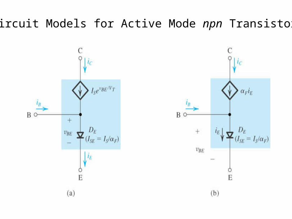
Circuit Models for Active Mode npn Transistor

Practical Implementation
E and C are not symmetrical.
pnp transistors works dual to npn transistors much inthe same way PMOSFET works dual to NMOSFET.(In this class, we will concentrate on npn transistors.)

Circuit Symbols for npn Transistors
Biasing in active modeDirections of current flow
Example: Given 100. When 1 mA, 0.7 .
Design to achieve 2 mA when 5 V.
Since 5 V 5 V (reverse biased)
Transistor is in active mode.
15 55 k
2
ln
A
BE
T
C BE
C C
C B C
C
v
V CC S BE T
S
i v V
i V
V V V
R
ii I e v V
I
1t 1 mA, 0.7 ln .... (1)
2At 2 mA, ln .... (2)
Subtract (1) from (2)
20.7 ln 0.717 25 mV
1
100Given 100 0.99
100 12
2.02 mA0.99
0.717 ( 15)
2.0
C TS
C BE TS
BE T T
CE
C
i VI
i v VI
v V V
ii
R
7.07 k
2

iC – vBE Characteristics
Temperature Dependence
is typically 0.6 V to 0.8 V
BE
T
v
VC S
BE
i I e
v

Common Base Characteristics
Base voltage is fixed at zero.In active region, vCB ≥ - 0.4 V
Large signal Small signal C C
E E
i i
i i

Dependence of iC on Collector Voltage
50 V to 100 V (Early Voltage)
1BE
T
A
v
V CEC S
A
V
vi I e
V
0A CE
C
V Vr
I
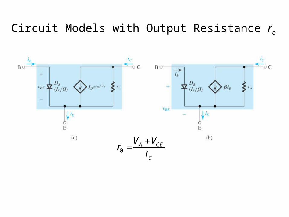
Circuit Models with Output Resistance ro

Common Emitter Configuration
constant
Large signal Small signal CE
CQ Cdc
BQ B v
I i
I i

sat
satforced
forced
forced
In saturation, <
: current ratio in saturation
: overdrive factor
C B
C
B
I I
I
I

off 0.1 VCEV
Common Emitter Saturation Model
sat off sat sat
sat
sat
is typically 0.1 V to 0.3 V.
is much larger than typical triode voltages of .
BJT is less attractive than CMOS for logic circuits.
CE CE C CE
CE
CE DS
V V I R
V
V V

Designing Linear Amplifiers (Active Region)
and
cutoff if 0.5 VBJT is
active if > 0.5 V
Initially after BJT turns on, large.
Further increase of , gets small.
BE I I
T T T
O CE CC C C I BE
I
I
CE
I CE
v v v
V V VC S S O CC C S
v v V R i v v
v
v
v
v v
i I e I e v V R I e
satsat
sat
In saturation,
0.1 V to 0.2 V
CC CEC
C
CE
V VI
R
V

Amplifier Gain
max
1
BE
T
BE
T
I BE
V
VC S
CE CC C C
V
VOv S C
I TV V
C Cv
T
CCv
T
I I e
V V R I
vA I e R
v V
R IA
V
VA
V

15
3 15 0.025
3
Example: Common Emitter Circuit
Given 10 A, 6.8 k and 10 V
Find and for 3.2 V.
10 3.21 mA
6.8
1 10 1 10
690.8 10 V
10 3.2
0
BE BE
T
S C CC
BE C CE
CC CEC
C
V VV
C S
BE
CC CEv
T
I R V
V I V
V VI
R
I I e e
V
V VA
V
3
272 V/V.025
Assume at the edge of saturation 0.3 V.
10 0.31.617 mA
6.8
new 1.617ln 0.025ln 12 10 V
old 1
CE
CC CEC
C
CBE T
C
v
V Vi
R
iv V
i

Graphical Analysis
Get from the graph
BE
T
CE CC C C CC C B
v
VC SB
B
v V R i V R i
i Ii e
i
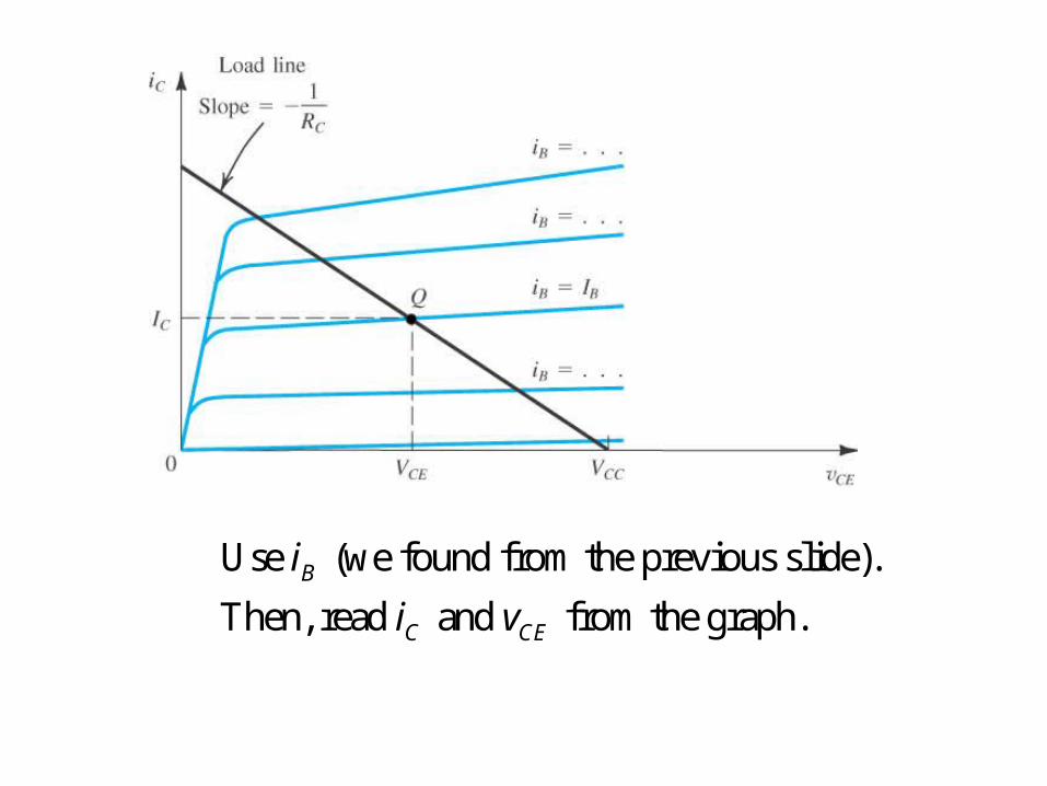
Use (we found from the previous slide).
Then, read and from the graph.B
C CE
i
i v

To determine iB, iC and vCE, you need to use both graphs.
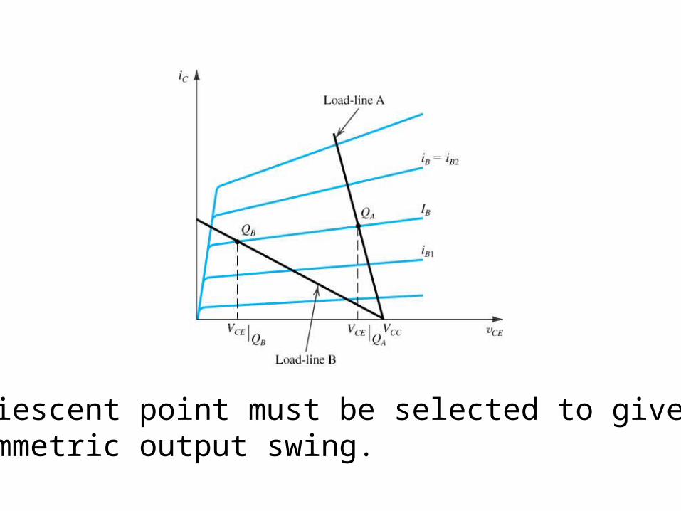
Quiescent point must be selected to give a symmetric output swing.

(EOS
Switching Operation
0.5 V (cutoff) 0, 0 and
0.5 V and 0.4 (active)
, and
0.5 V and = 0.4
(edge of saturation - EOS)
I B C C CC
I C B
I BEB C B C CC C C
B
I C B
C
v i i v V
v v v
v vi i i v V R i
R
v v v
i
(EOS)) (EOS) (EOS) (EOS)
satsat
satforced
0.3, and
0.5 V and < 0.4 (saturation)
In deep saturation:
CCCB I B B BE
C
I C B
CC CEC
C
C
B
ivi V I R V
R
v v v
V VI
R
I
I

sat
forced
When the transistor is on:
0.7 V
0.2 V
In active mode: 0.4
In saturation mode: 0.4
Check: for active mode,
DC Analysis Model
BE
CE
CB
CB
C C
B B
V
V
V
V
I I
I I
for saturation mode
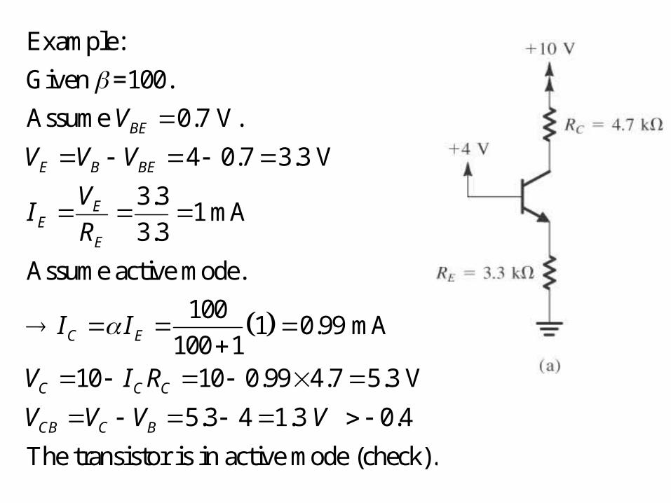
Example:
Given =100.
Assume 0.7 V.
4 0.7 3.3 V
3.31 mA
3.3
Assume active mode.
1001 0.99 mA
100 110 10 0.99 4.7 5.3 V
5.3 4 1.3 0.4
The transistor is in ac
BE
E B BE
EE
E
C E
C C C
CB C B
V
V V V
VI
R
I I
V I R
V V V V
tive mode (check).
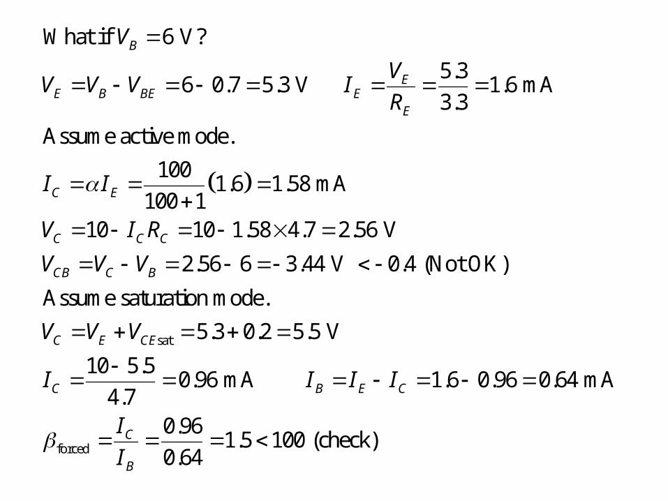
What if 6 V?
5.36 0.7 5.3 V 1.6 mA
3.3
Assume active mode.
1001.6 1.58 mA
100 110 10 1.58 4.7 2.56 V
2.56 6 3.44 V 0.4 (Not OK)
Assume saturation mode.
B
EE B BE E
E
C E
C C C
CB C B
V
VV V V I
R
I I
V I R
V V V
V
sat
forced
5.3 0.2 5.5 V
10 5.50.96 mA 1.6 0.96 0.64 mA
4.70.96
1.5 100 (check)0.64
C E CE
C B E C
C
B
V V
I I I I
I
I

What if 0 V?
Transistor is cutoff.
0 V
0 V
10 V
0 A
B
E
B
C
B C E
V
V
V
V
I I I
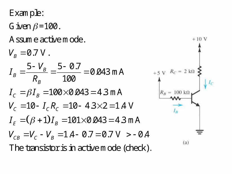
Example:
Given =100.
Assume active mode.
0.7 V.
5 5 0.70.043 mA
100
100 0.043 4.3 mA
10 10 4.3 2 1.4 V
1 101 0.043 4.3 mA
1.4 0.7 0.7 V 0.4
The transistor is in a
B
BB
B
C B
C C C
E B
CB C B
V
VI
R
I I
V I R
I I
V V V
ctive mode (check).

2
1 2
1 2
Example: Given =100.
Note that 0.
Thus we need to find an equivalent
circuit for the input part.
15 5 V
|| 33.3 k
B
BBB
B B
BB B B
I
RV
R R
R R R
Input part
+_ VBB_
+
10 V
RB1
RB2
10 V RB2VBB
RB1
+_VBB
RBB

Assume active mode.
1
5 0.71.29 mA
33.33
1011
1.290.0128 mA
1 101
0.7 1.29 3 4.57 V
0.99 1.29 1.28 mA
15 15
BB B BB BE E E
EBB BE E E
BB BEE
BBE
EB
B BE E E
C E
C C C
V I R V I R
IR V I R
V VI
RR
II
V V I R
I I
V I R
1.28 5 8.6 V
> 8.6 4.57 4.04 0.4
The transistor is in active mode (check).CB C BV V V

Biasing BJT• Determining a quiescent point for linearization
• Active mode operation
• Considerations– Stable with respect to manufacturing parameters
(e.g., ro, β)
– Desired gains– Acceptable output swing
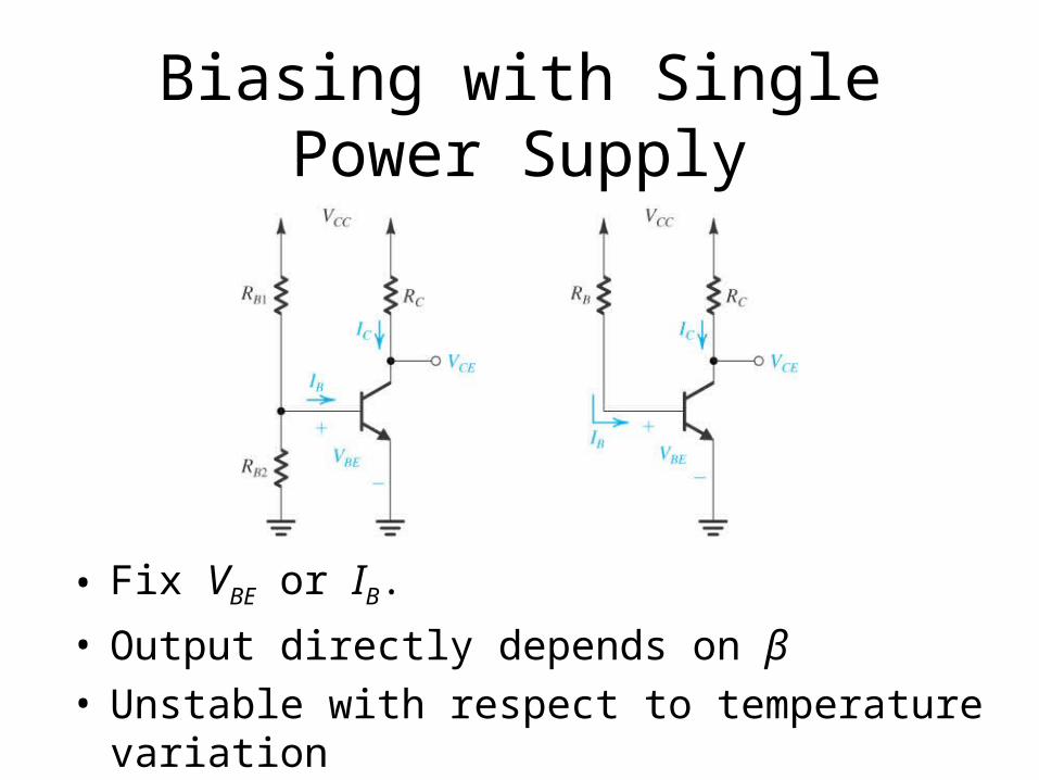
Biasing with Single Power Supply
• Fix VBE or IB.
• Output directly depends on β• Unstable with respect to temperature variation

Addition of Degeneration Resistor
2 1 21 2
1 2 1 2
|| =
1
To stablize the design: and 1
1Good rule of thumb:
3
BB BEBB CC B E
BE
BBB BE E
BB CB C C CC
R R R V VV V R R R I
RR R R R R
RV V R
V V I R V
1 2
1 2
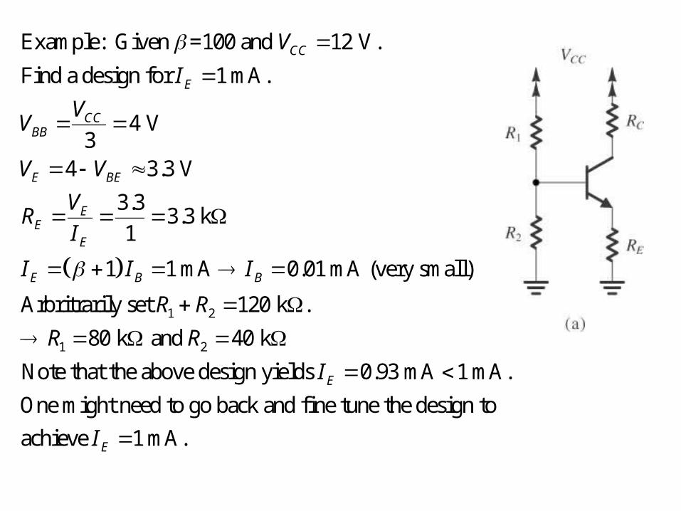
Example: Given =100 and 12 V.
Find a design for 1 mA.
4 V3
4 3.3 V
3.33.3 k
1
1 1 mA 0.01 mA (very small)
Arbritrarily set 120 k .
80 k and 40 k
Note
CC
E
CCBB
E BE
EE
E
E B B
V
I
VV
V V
VR
I
I I I
R R
R R
that the above design yields 0.93 mA 1 mA.
One might need to go back and fine tune the design to
achieve 1 mA.
E
E
I
I
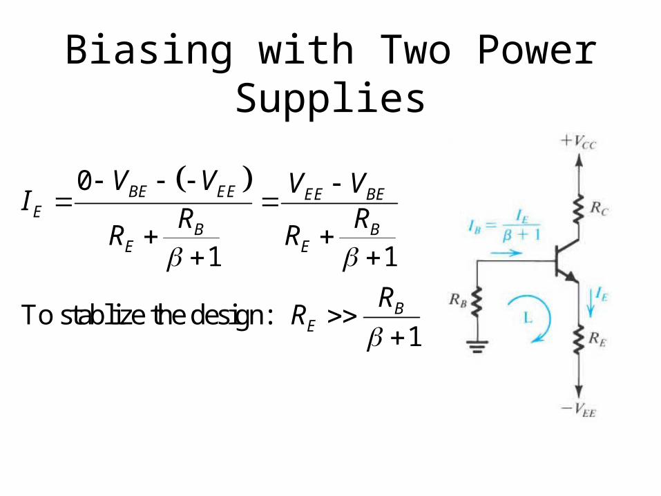
Biasing with Two Power Supplies
0
1 1
To stablize the design: 1
BE EE EE BEE
B BE E
BE
V V V VI
R RR R
RR

Biasing with Feedback Resistor
1
1
If , is stable.1
ECC E C B B BE E C B BE
CC BEE
BC
BC E
IV I R I R V I R R V
V VI
RR
RR I

Biasing with Current Source
1 2
1
1
1 2
and are matched.
has base and collector shorted.
is a diode.
Since 's are the same for and
CC EE BEREF
BE
CC EE BEREF
Q Q
Q
Q
V V VI
RV Q Q
V V VI I
R

Small Signal Analysis
• A quiescent point has been determined by biasing.
• Active mode operation– Forward biasing for base-emitter junction by VBE
– Reverse biasing for collector-base junction by RC and VCC

Consider dc first.
0.4 (active mode)
BE
T
V
VC S
CE
CB
C CE CC C C
C B
I I e
II
II
V V V R I
V V
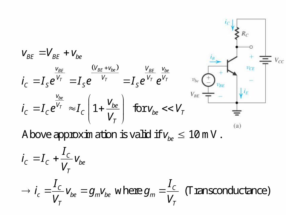
1 for
Above approximation is valid if 10 mV.
where (Transconductance)
BE be beBE BE
T T T T
be
T
BE BE be
V v vv V
V V V VC S S S
v
V beC C C be T
T
be
CC C be
T
C Cc be m be m
T T
v V v
i I e I e I e e
vi I e I v V
V
v
Ii I v
V
I Ii v g v g
V V
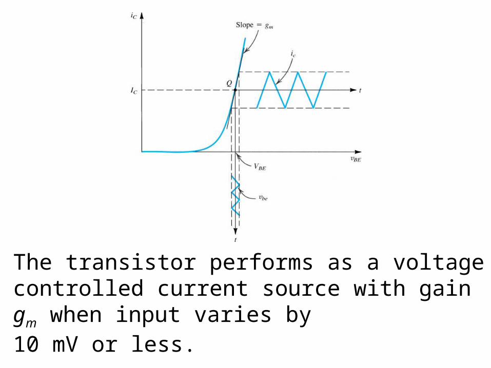
The transistor performs as a voltage controlled current source with gain gm when input varies by 10 mV or less.

1
Input resistance between base and emitter
C C CB be
T
mb be
be T
b m B
i I Ii v
V
gi v
v Vr
i g I

1
1
Input resistance between base and emitter
1
1
C C CE be
T
C Ee be be
T T
be Te
e E m m
ebe b e e e e
b
i I Ii v
V
I Ii v v
V V
v Vr
i I g g
iv i r i r r r r
i

C CC C C
C CC C c C
C CC C C c C
C C c C
c c C m be C
c m C be v be
c C Cv m C
be T
v V i R
v V I i R
v V I R i R
v V i R
v i R g v R
v g R v A v
v I RA g R
v V
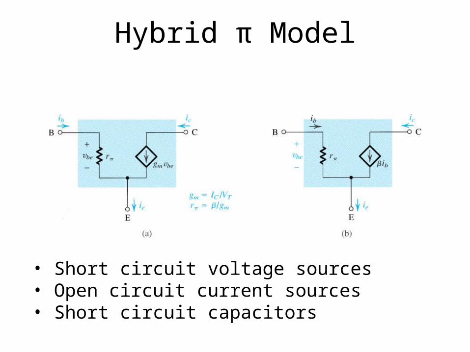
Hybrid π Model
• Short circuit voltage sources• Open circuit current sources• Short circuit capacitors

1
1
1
be bee m be m
be be bee
e
m be m b
m b b
v vi g v g r
r r
v v vi
rr r
g v g i r
g r i i

T Model
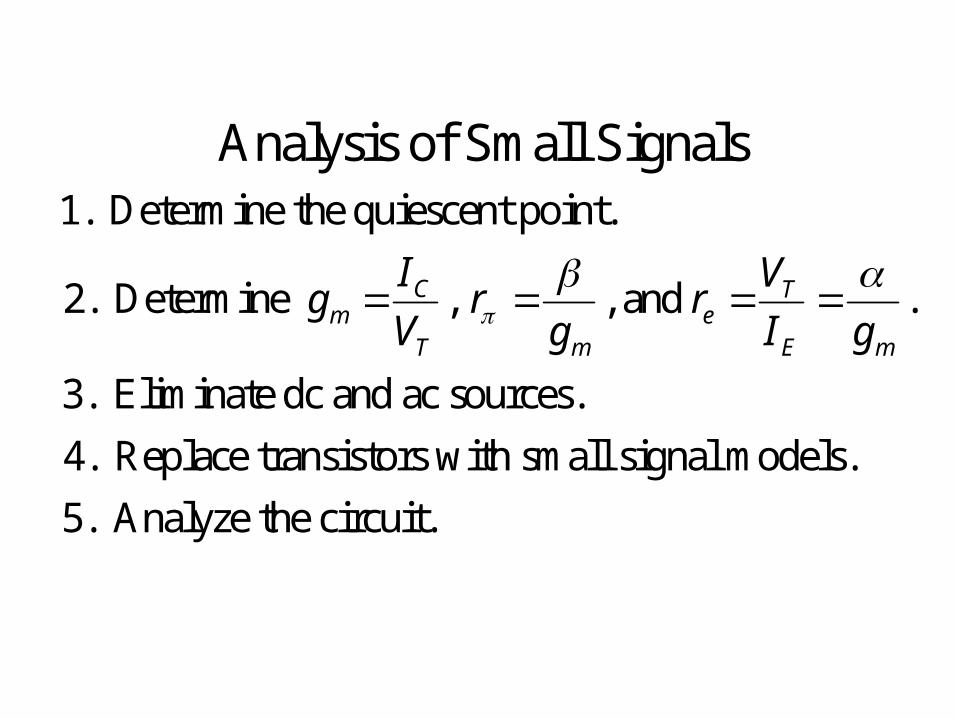
1. Determine the quiescent point.
2. Determine , , and .
3. Eliminate dc and ac sources.
4. Replace transistors with small signal mode
Analysis of Small Signals
C Tm e
T m E m
I Vg r r
V g I g
ls.
5. Analyze the circuit.

Example: Given =100 and 10 V.
Assume 0 V.
0.991
3 0.70.023 mA
100
100 0.023 2.3 mA
10 2.3 3 3.1 V
3.1 V > 0.3 V Transistor in active mode
25 mV2.
CC
i
BB BEB
BB
C B
C CC C C
CE
Te
E
V
v
V VI
R
I I
V V I R
V
Vr
I
10.8 3 mA0.992.3 mA
92 mA/V25 mV
1001.09 k
92
Cm
T
m
Ig
V
rg

Now ac analysis
1.090.011
101.09
92 0.011 3 3.04
3.04
be i i iBB
o m be C i i
ov
i
rv v v v
r R
v g v R v v
vA
v

Hybrid π Model with Early Effect
||
A CE Ao
C C
o m be C o
V V Vr
I I
v g v R r

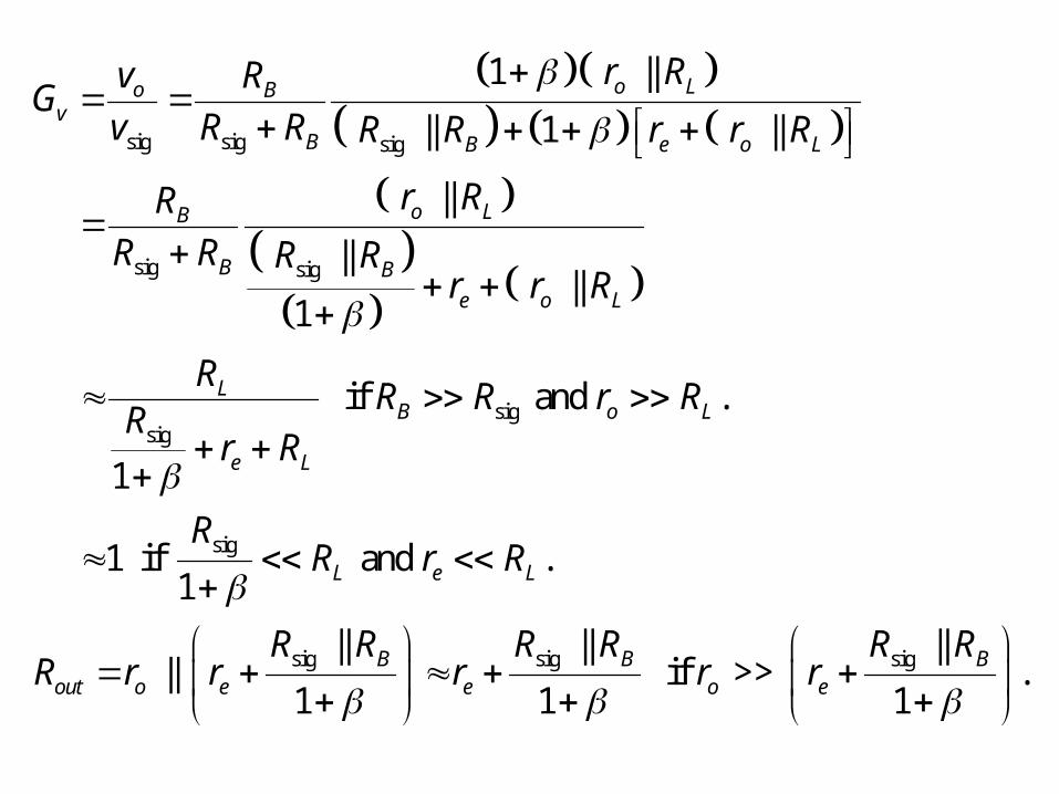
Structure of Single Stage Amplifier

Common Emitter Amplifier

sig sig sig
sig sig sig
|| where .
if .
|| if .
||
iin B ib ib
i
in B
Bini B
in B
i
vR R R R r
i
R r R r
R rR rv v v v R r
R R R r R r R
v v
sig sig
|| ||
|| ||
|| if .
|| if .
for unilateral amplifier.
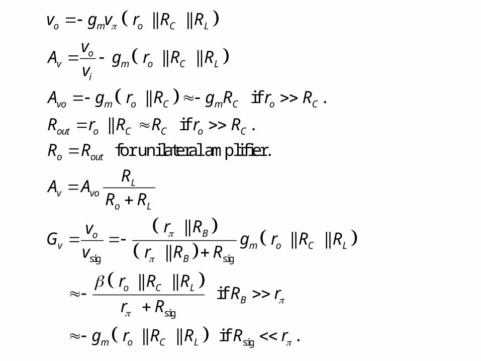
|| ||
||
o m o C L
ov m o C L
i
vo m o C m C o C
out o C C o C
o out
Lv vo
o L
Bov m o
B
v g v r R R
vA g r R R
v
A g r R g R r R
R r R R r R
R R
RA A
R R
r RvG g r
v r R R
sig
sig
||
|| || if
|| || if .
C L
o C LB
m o C L
R R
r R RR r
r R
g r R R R r

Common Emitter Amplifier with RE
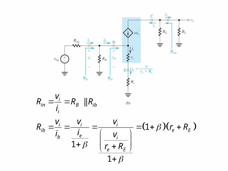
||
1
1
1
iin B ib
i
i i iib e E
eb i
e E
vR R R
i
v v vR r R
ii v
r R

sig sig
sig
|| ||
|| ||
||
1
||
|| if
1
o c C L e C L
e C L C Lov
i e e E e E
C Lv
e E
C m Cvo
e E m E
out C
C Lo inv
in e E
C Lv E ib
e E
v i R R i R R
i R R R RvA
v i r R r R
R RA
r R
R g RA
r R g R
R R
R Rv RG
v R R r R
R RG R R
R r R

Common Base Amplifier
iin e
i
vR r
i

sig sig sig sig
||
|| ||
|| || ||
o e C L
ie
e
ov C L m C L
i e
vo m C
out C
C L C Lo ev m C L
e e e
v i R R
vi
r
vA R R g R R
v r
A g R
R R
R R R Rv rG g R R
v R r R r R r

Common Collector Amplifier

||
1 ||
iin B ib
i
iib e o L
b
vR R R
i
vR r r R
i

sig sig sig
sig sig
sigsig
sig
1 ||
|| 1 ||
||
|| ||
1
if and .
1
1 if and .1
o Lo Bv
B B e o L
o LB
B B
e o L
LB o L
e L
L e L
r Rv RG
v R R R R r r R
r RR
R R R Rr r R
RR R r R
Rr R
RR r R
sig sig sig
|| || || || if >> .
1 1 1B B B
out o e e o e
R R R R R RR r r r r r
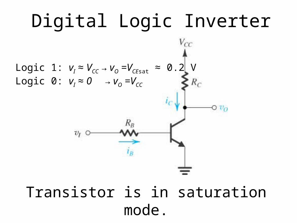
Digital Logic Inverter
Transistor is in saturation mode.
Logic 1: vI ≈ VCC → vO =VCEsat ≈ 0.2 V Logic 0: vI ≈ 0 → vO =VCC

vI – vO Transfer Function
VCC = 5 VRB = 10 kΩRC = 1 kΩβ = 50

sat
sat
1. If 0.2 V 5 V
2. 0.7 V
3. Transistor in active region
1 50 V/V
10
4. Edge of saturation
I OL CE O OH CC
IL
IL I IH
o C Cv
i B B
I IH
CC CE
CB
v V V v V V
V
V v V
v R RA
v r R R
v V
V V
RI
sat
sat
forced
0.096 mA
1.66 V
5. 5 V
4.8 11 50
0.43
6. 5 1.66 3.44 V
0.7 0.2 0.5 V
CC CE
C
IH B B BE
I OH
CC CE
C
OH BE
B
H OH IH
L IL OL
V V
R
V I R V
v V
V V
RV V
R
NM V V
NM V V