Embed Size (px)
Citation preview

ECE 335: Electronic Circuits
Lecture 6:
MOSFET Large Signal Model
Faculty of EngineeringFaculty of EngineeringFaculty of EngineeringFaculty of Engineering
• Based on content from
Sedra/Smith “Microelectronic Circuits” -
Fifth Edition
2

3
Figure 4.1 Physical structure of the enhancement-type NMOS transistor: (a) perspective view; (b) cross-section. Typically L = 0.1 to 3 µm, W = 0.2 to
100 µm, and the thickness of the oxide layer (tox) is in the range of 2 to 50 nm.
MOSFET
4
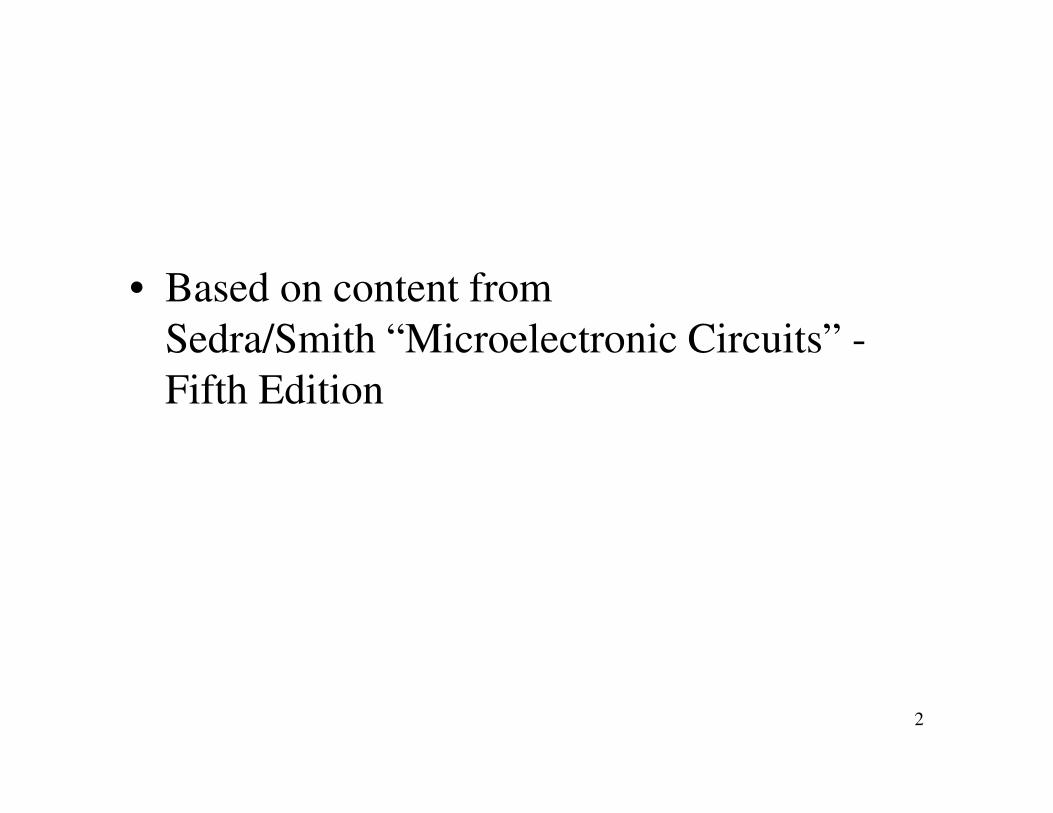
Figure 4.2 The enhancement-type NMOS transistor with a positive voltage applied to the gate. An n channel is induced at
the top of the substrate beneath the gate.
Enhancement NMOS
5
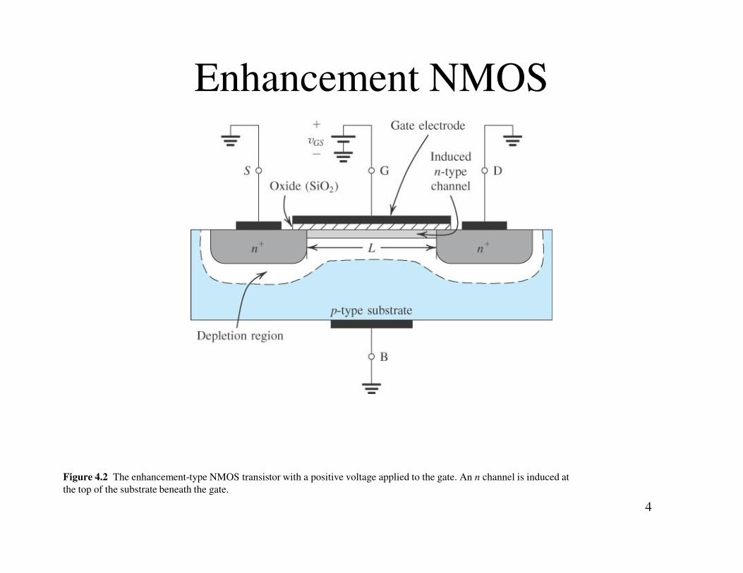
Figure 4.3 An NMOS transistor with vGS > Vt and with a small vDS applied. The device acts as a resistance whose value is
determined by vGS. Specifically, the channel conductance is proportional to vGS – Vt’ and thus iD is proportional to (vGS – Vt) vDS.
Note that the depletion region is not shown (for simplicity).
Linear Mode
6
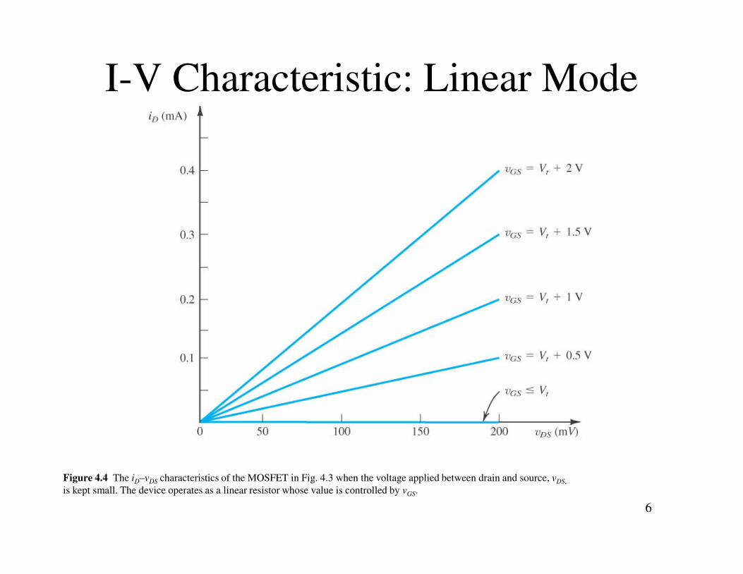
Figure 4.4 The iD–vDS characteristics of the MOSFET in Fig. 4.3 when the voltage applied between drain and source, vDS,
is kept small. The device operates as a linear resistor whose value is controlled by vGS.
I-V Characteristic: Linear Mode

7
Figure 4.5 Operation of the enhancement NMOS transistor as vDS is increased. The induced channel acquires a tapered
shape, and its resistance increases as vDS is increased. Here, vGS is kept constant at a value > Vt.
Linear Mode (2)

8
Figure 4.6 The drain current iD versus the drain-to-source voltage vDS for an enhancement-type NMOS transistor operated
with vGS > Vt.
Ideal I-V Characteristic
9
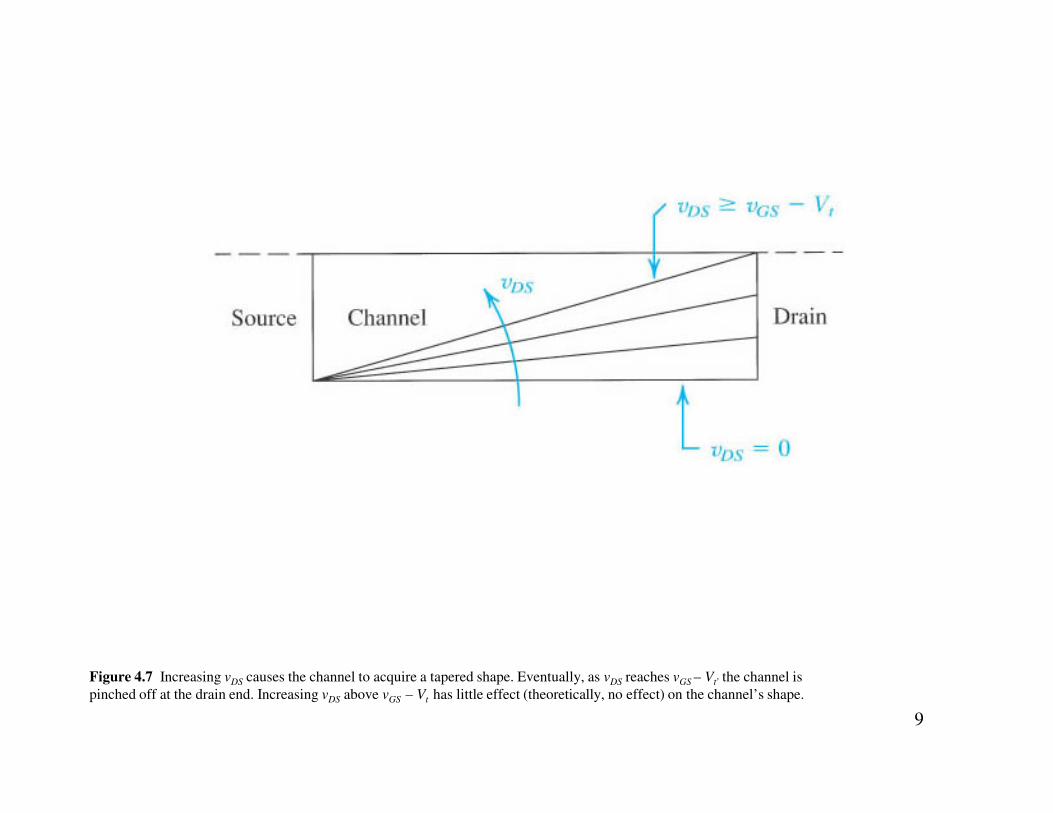
Figure 4.7 Increasing vDS causes the channel to acquire a tapered shape. Eventually, as vDS reaches vGS – Vt’ the channel is
pinched off at the drain end. Increasing vDS above vGS – Vt has little effect (theoretically, no effect) on the channel’s shape.
10
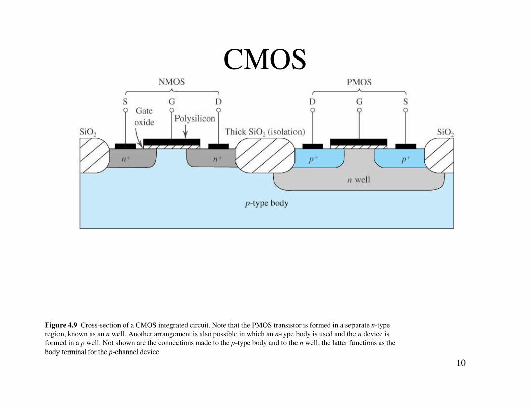
Figure 4.9 Cross-section of a CMOS integrated circuit. Note that the PMOS transistor is formed in a separate n-type
region, known as an n well. Another arrangement is also possible in which an n-type body is used and the n device is
formed in a p well. Not shown are the connections made to the p-type body and to the n well; the latter functions as the
body terminal for the p-channel device.
CMOS

11
Figure 4.10 (a) Circuit symbol for the n-channel enhancement-type MOSFET. (b) Modified circuit symbol with an
arrowhead on the source terminal to distinguish it from the drain and to indicate device polarity (i.e., n channel). (c)
Simplified circuit symbol to be used when the source is connected to the body or when the effect of the body on device
operation is unimportant.
Circuit Symbols

12
Figure 4.11 (a) An n-channel enhancement-type MOSFET with vGS and vDS applied and with the normal directions of
current flow indicated. (b) The iD–vDS characteristics for a device with k’n (W/L) = 1.0 mA/V2.

13
Figure 4.12 The iD–vGS characteristic for an enhancement-type NMOS transistor in saturation (Vt = 1 V, k’n W/L = 1.0
mA/V2).
14
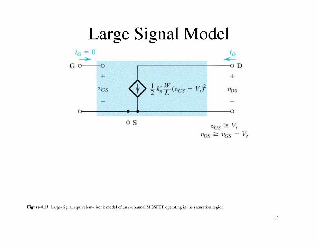
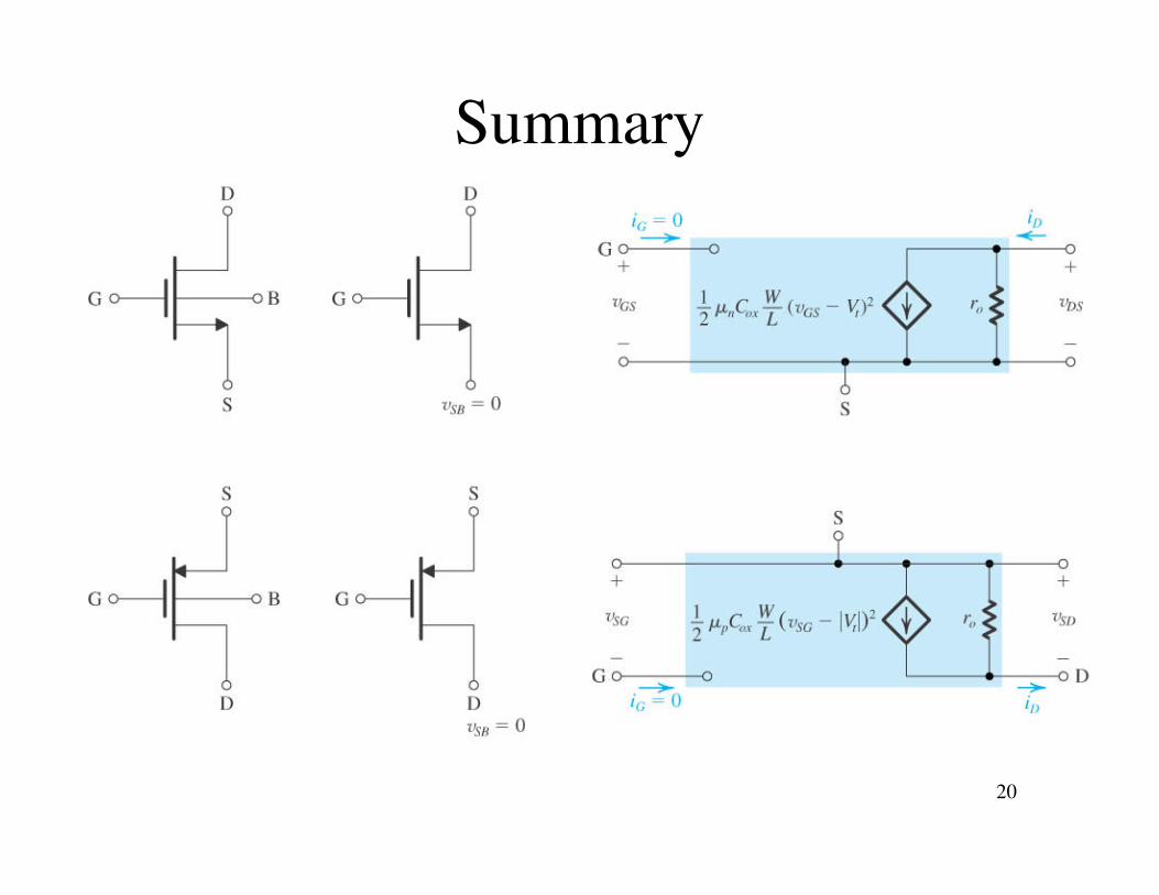
Figure 4.13 Large-signal equivalent-circuit model of an n-channel MOSFET operating in the saturation region.
Large Signal Model
15
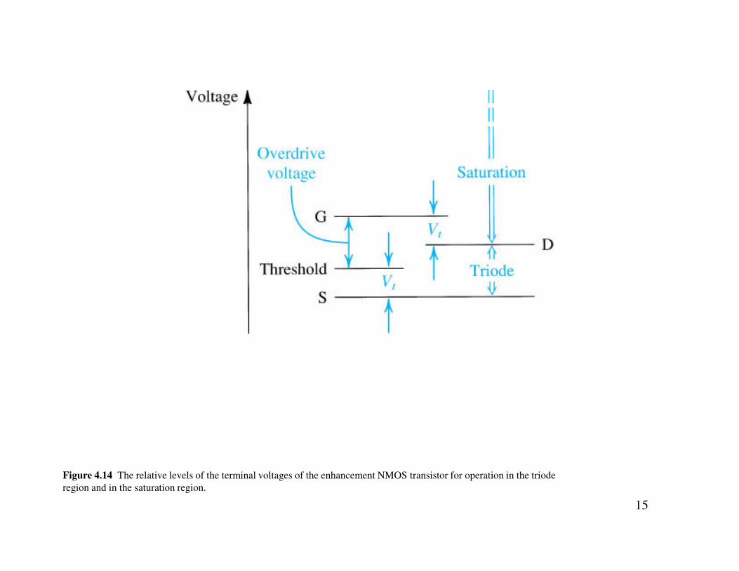
Figure 4.14 The relative levels of the terminal voltages of the enhancement NMOS transistor for operation in the triode
region and in the saturation region.
16
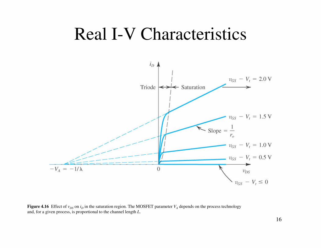
Figure 4.16 Effect of vDS on iD in the saturation region. The MOSFET parameter VA depends on the process technology
and, for a given process, is proportional to the channel length L.
Real I-V Characteristics
17
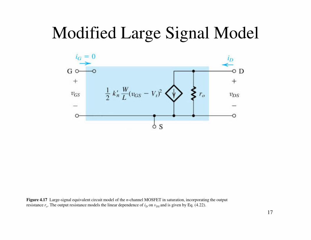
Figure 4.17 Large-signal equivalent circuit model of the n-channel MOSFET in saturation, incorporating the output
resistance ro. The output resistance models the linear dependence of iD on vDS and is given by Eq. (4.22).
Modified Large Signal Model
18
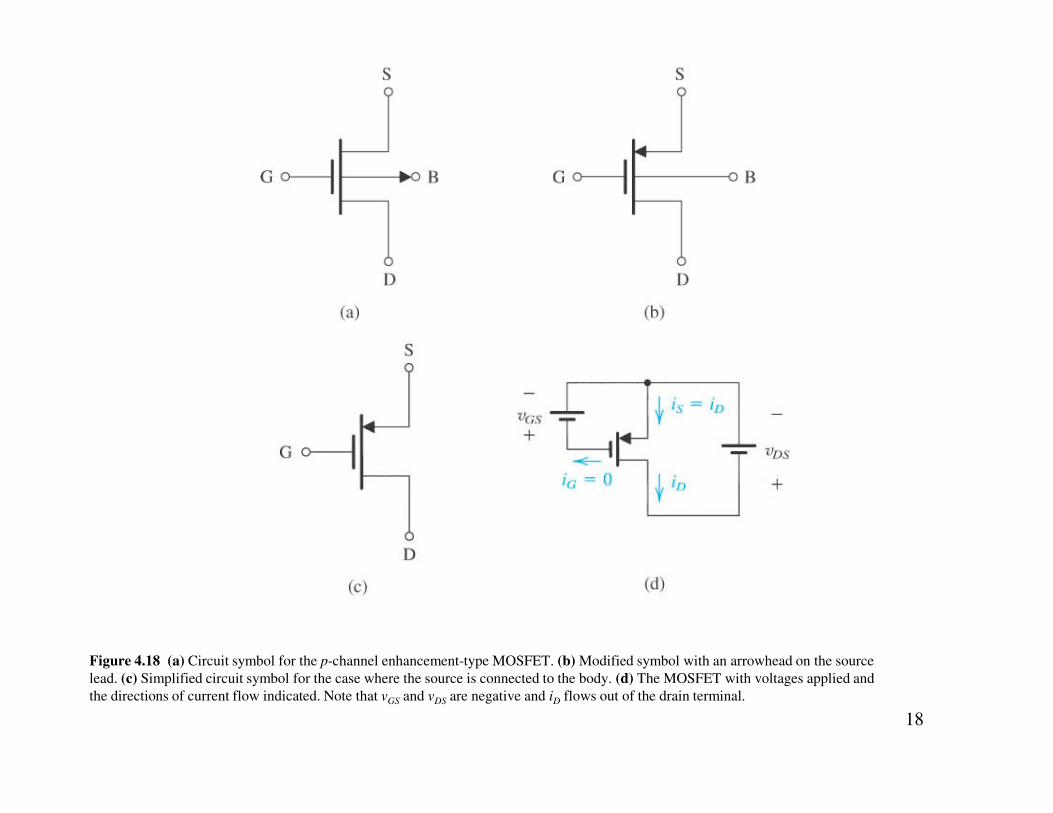
Figure 4.18 (a) Circuit symbol for the p-channel enhancement-type MOSFET. (b) Modified symbol with an arrowhead on the source
lead. (c) Simplified circuit symbol for the case where the source is connected to the body. (d) The MOSFET with voltages applied and
the directions of current flow indicated. Note that vGS and vDS are negative and iD flows out of the drain terminal.
19
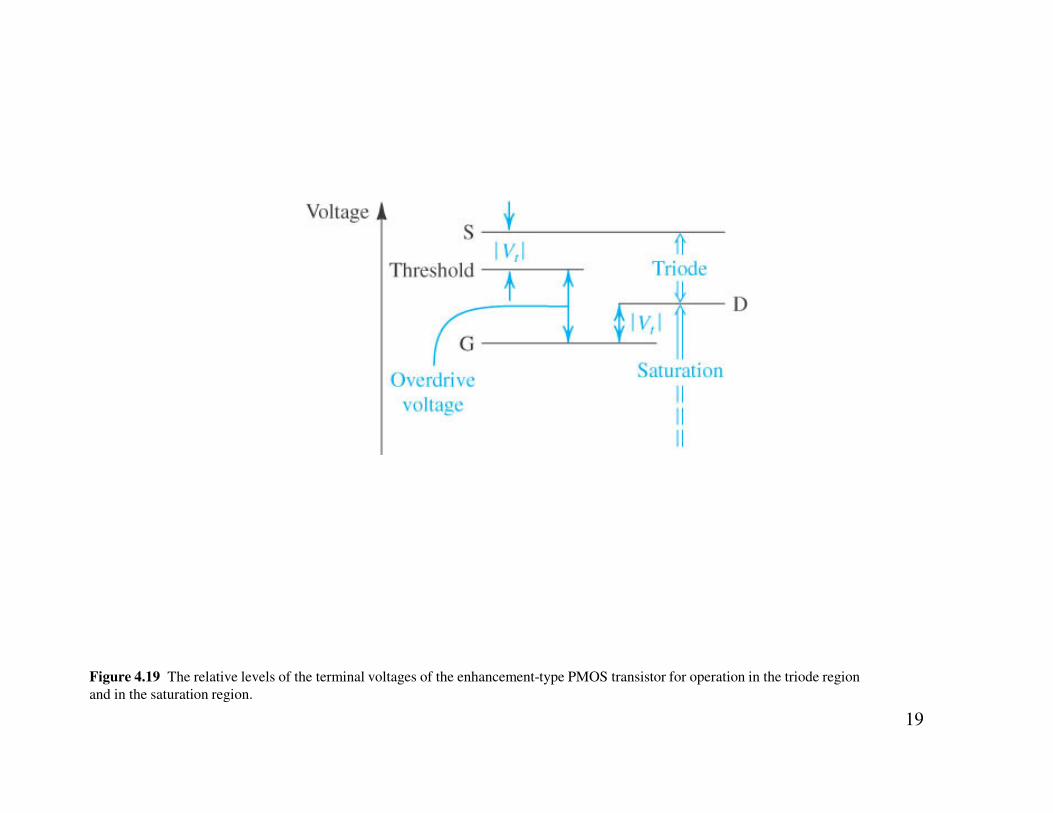
Figure 4.19 The relative levels of the terminal voltages of the enhancement-type PMOS transistor for operation in the triode region
and in the saturation region.
20
Summary