Embed Size (px)
Citation preview
Lecture 2: MIPS Processor Example
2: MIPS Processor Example 2CMOS VLSI DesignCMOS VLSI Design 4th Ed.
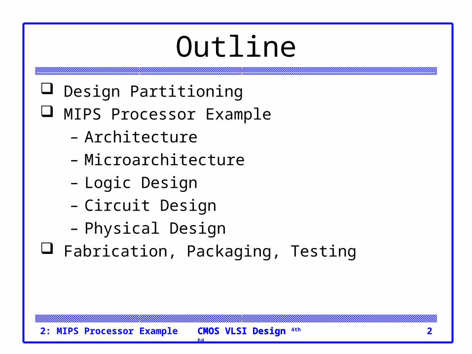
Outline Design Partitioning MIPS Processor Example
– Architecture– Microarchitecture– Logic Design– Circuit Design– Physical Design
Fabrication, Packaging, Testing
2: MIPS Processor Example 3CMOS VLSI DesignCMOS VLSI Design 4th Ed.
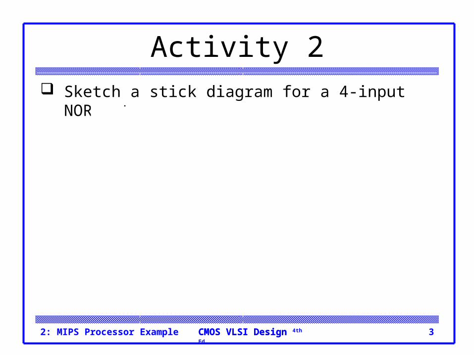
Activity 2 Sketch a stick diagram for a 4-input NOR gate
AVDD
GND
B C
Y
D
2: MIPS Processor Example 4CMOS VLSI DesignCMOS VLSI Design 4th Ed.
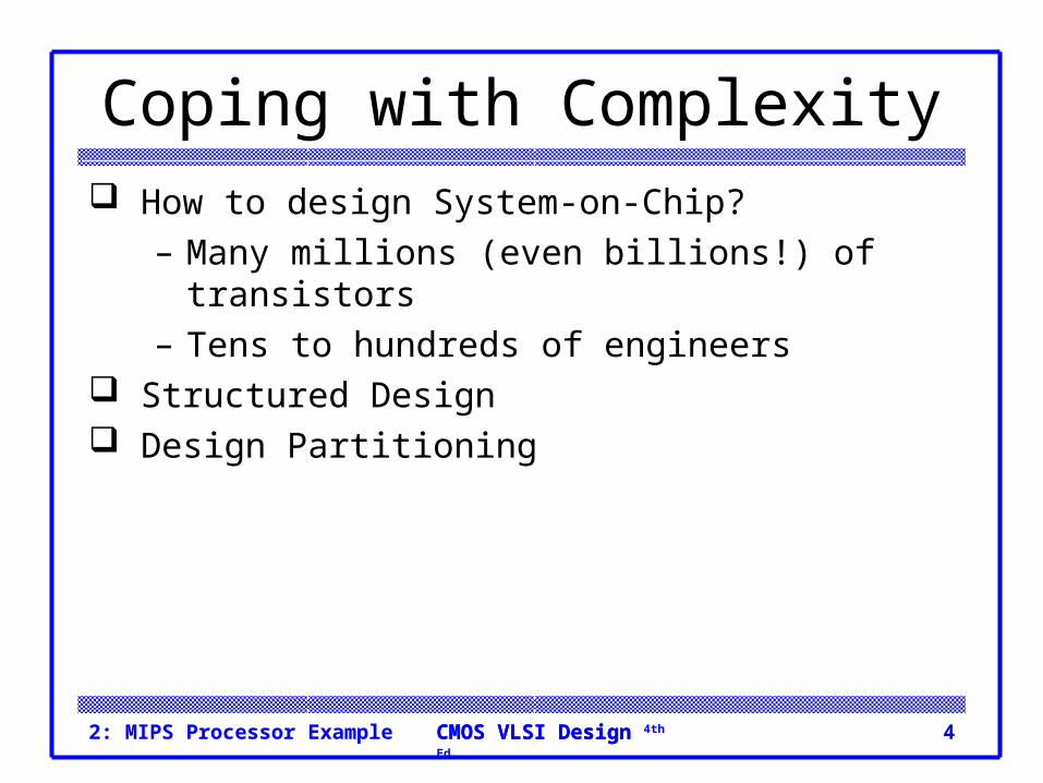
Coping with Complexity How to design System-on-Chip?
– Many millions (even billions!) of transistors– Tens to hundreds of engineers
Structured Design Design Partitioning
2: MIPS Processor Example 5CMOS VLSI DesignCMOS VLSI Design 4th Ed.
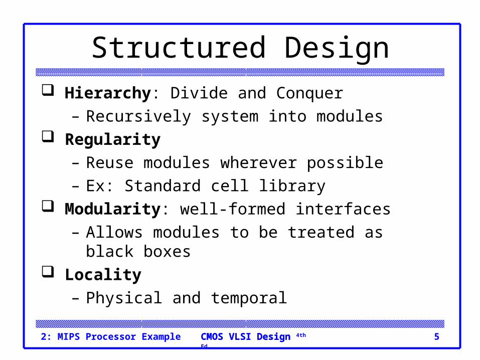
Structured Design Hierarchy: Divide and Conquer
– Recursively system into modules Regularity
– Reuse modules wherever possible– Ex: Standard cell library
Modularity: well-formed interfaces– Allows modules to be treated as black boxes
Locality– Physical and temporal
2: MIPS Processor Example 6CMOS VLSI DesignCMOS VLSI Design 4th Ed.
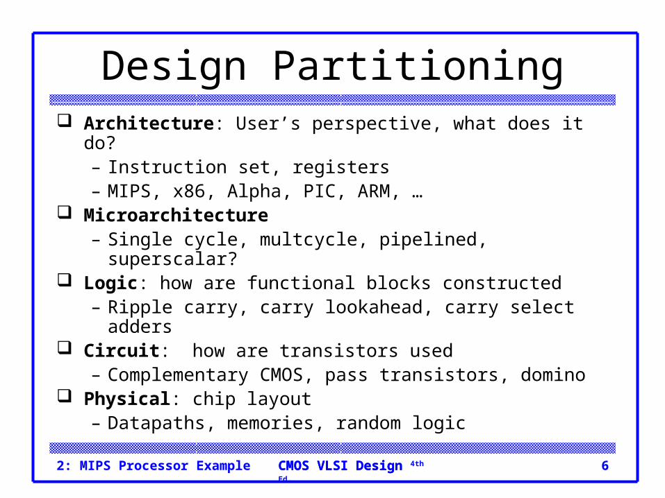
Design Partitioning Architecture: User’s perspective, what does it do?
– Instruction set, registers– MIPS, x86, Alpha, PIC, ARM, …
Microarchitecture– Single cycle, multcycle, pipelined, superscalar?
Logic: how are functional blocks constructed– Ripple carry, carry lookahead, carry select adders
Circuit: how are transistors used– Complementary CMOS, pass transistors, domino
Physical: chip layout– Datapaths, memories, random logic
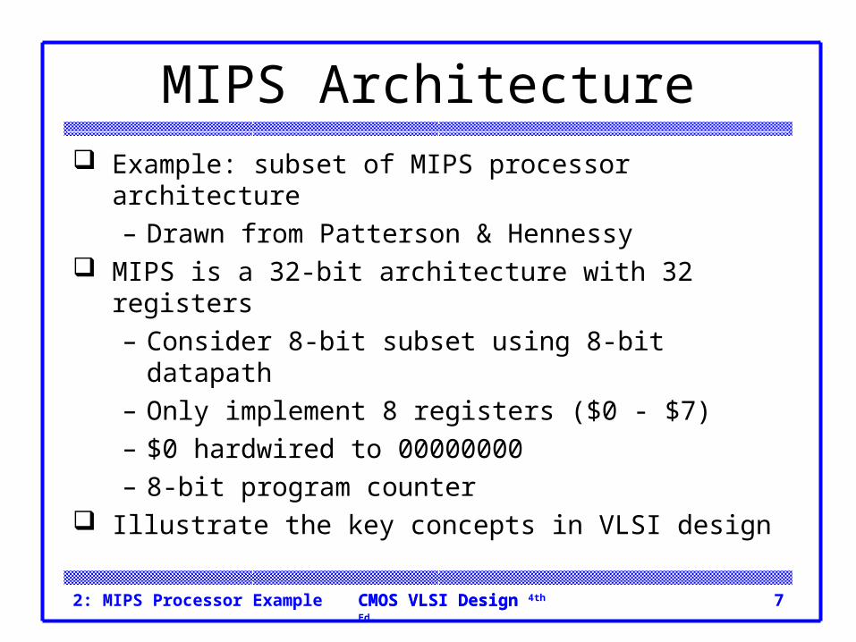
2: MIPS Processor Example 7CMOS VLSI DesignCMOS VLSI Design 4th Ed.
MIPS Architecture Example: subset of MIPS processor architecture
– Drawn from Patterson & Hennessy MIPS is a 32-bit architecture with 32 registers
– Consider 8-bit subset using 8-bit datapath– Only implement 8 registers ($0 - $7)– $0 hardwired to 00000000– 8-bit program counter
Illustrate the key concepts in VLSI design
2: MIPS Processor Example 8CMOS VLSI DesignCMOS VLSI Design 4th Ed.
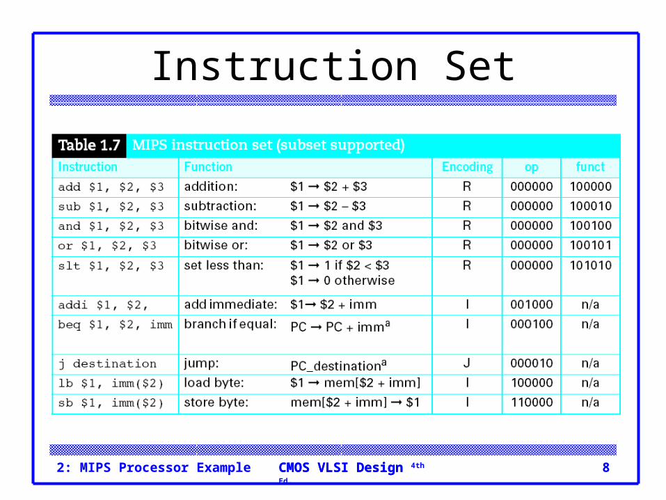
Instruction Set
2: MIPS Processor Example 9CMOS VLSI DesignCMOS VLSI Design 4th Ed.
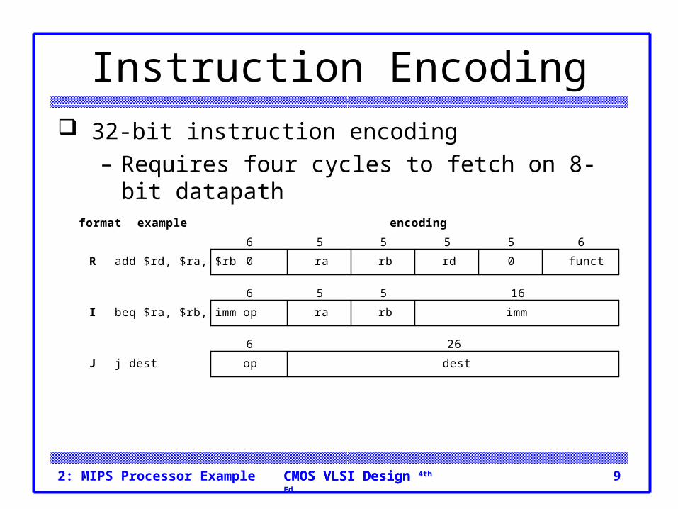
Instruction Encoding 32-bit instruction encoding
– Requires four cycles to fetch on 8-bit datapath
format example encoding
R
I
J
0 ra rb rd 0 funct
op
op
ra rb imm
6
6
6
65 5 5 5
5 5 16
26
add $rd, $ra, $rb
beq $ra, $rb, imm
j dest dest
2: MIPS Processor Example 10CMOS VLSI DesignCMOS VLSI Design 4th Ed.
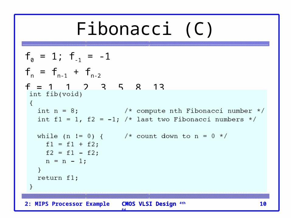
Fibonacci (C)f0 = 1; f-1 = -1
fn = fn-1 + fn-2
f = 1, 1, 2, 3, 5, 8, 13, …
2: MIPS Processor Example 11CMOS VLSI DesignCMOS VLSI Design 4th Ed.
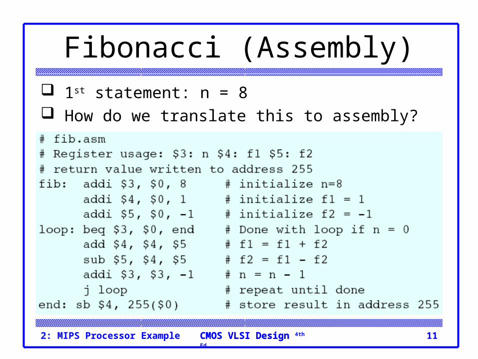
Fibonacci (Assembly) 1st statement: n = 8 How do we translate this to assembly?
2: MIPS Processor Example 12CMOS VLSI DesignCMOS VLSI Design 4th Ed.
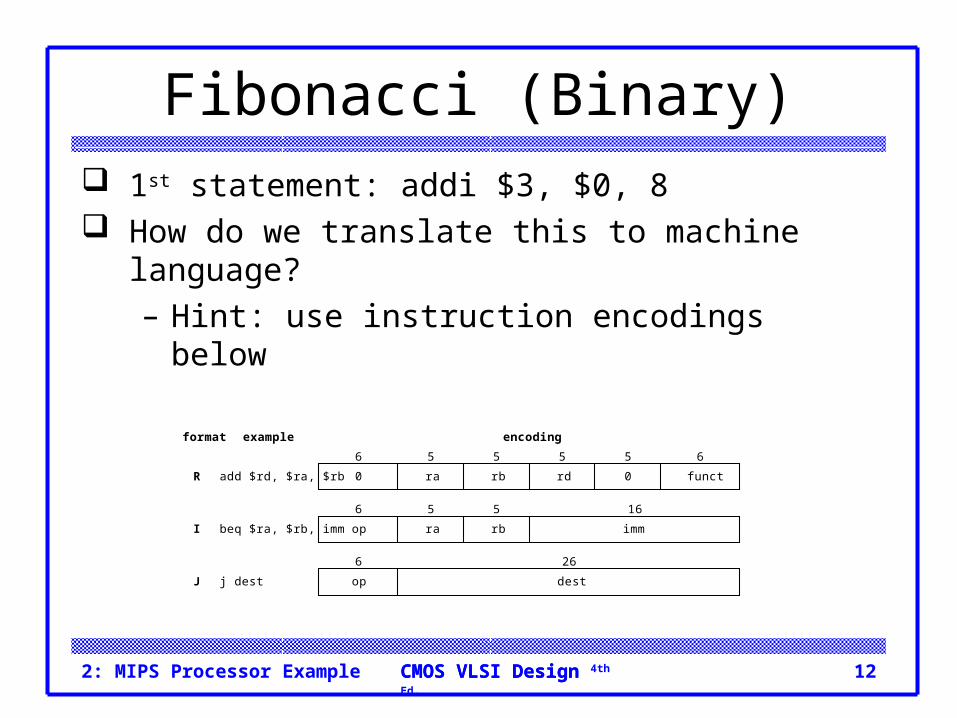
Fibonacci (Binary) 1st statement: addi $3, $0, 8 How do we translate this to machine language?
– Hint: use instruction encodings below
format example encoding
R
I
J
0 ra rb rd 0 funct
op
op
ra rb imm
6
6
6
65 5 5 5
5 5 16
26
add $rd, $ra, $rb
beq $ra, $rb, imm
j dest dest
2: MIPS Processor Example 13CMOS VLSI DesignCMOS VLSI Design 4th Ed.
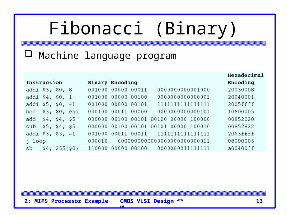
Fibonacci (Binary) Machine language program
2: MIPS Processor Example 14CMOS VLSI DesignCMOS VLSI Design 4th Ed.
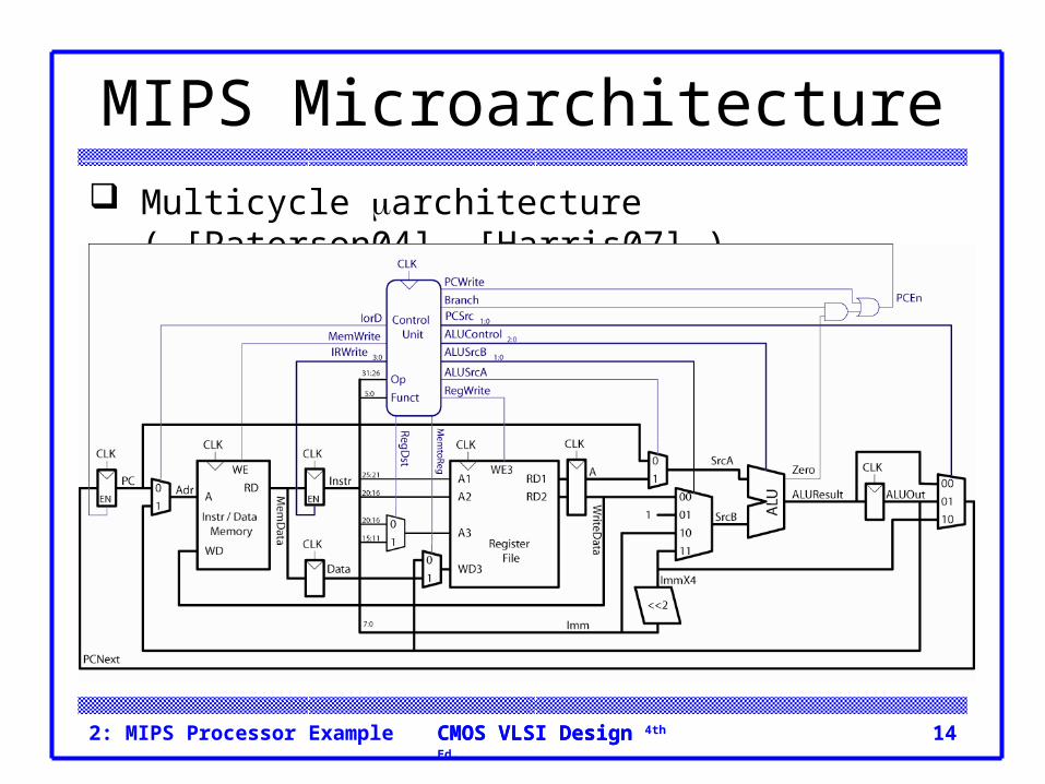
MIPS Microarchitecture Multicycle architecture ( [Paterson04], [Harris07] )

2: MIPS Processor Example 15CMOS VLSI DesignCMOS VLSI Design 4th Ed.
Multicycle Controller
PCWritePCSource = 10
ALUSrcA = 1ALUSrcB = 00ALUOp = 01PCWriteCond
PCSource = 01
ALUSrcA =1ALUSrcB = 00ALUOp= 10
RegDst = 1RegWrite
MemtoReg = 0
MemWriteIorD = 1
MemReadIorD = 1
ALUSrcA = 1ALUSrcB = 10ALUOp = 00
RegDst=0RegWrite
MemtoReg=1
ALUSrcA = 0ALUSrcB = 11ALUOp = 00
MemReadALUSrcA = 0
IorD = 0IRWrite3
ALUSrcB = 01ALUOp = 00
PCWritePCSource = 00
Instruction fetch
Instruction decode/register fetch
Jumpcompletion
BranchcompletionExecution
Memory addresscomputation
Memoryaccess
Memoryaccess R-type completion
Write-back step
(Op = 'LB ') or (Op = 'SB ') (Op = R-type)
(Op
='B
EQ')
(Op
='J
')
(Op
='S
B')
(Op
='L
B')
7
0
4
121195
1086
Reset
MemReadALUSrcA = 0
IorD = 0IRWrite2
ALUSrcB = 01ALUOp = 00
PCWritePCSource = 00
1MemRead
ALUSrcA = 0IorD = 0IRWrite1
ALUSrcB = 01ALUOp = 00
PCWritePCSource = 00
2MemRead
ALUSrcA = 0IorD = 0IRWrite0
ALUSrcB = 01ALUOp = 00
PCWritePCSource = 00
3
2: MIPS Processor Example 16CMOS VLSI DesignCMOS VLSI Design 4th Ed.
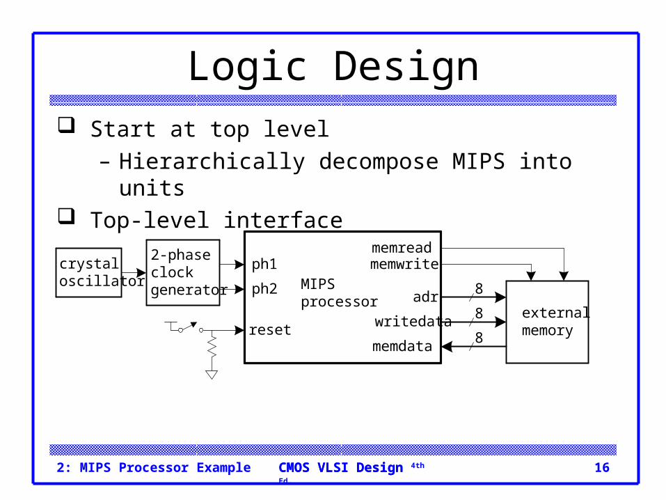
Logic Design Start at top level
– Hierarchically decompose MIPS into units Top-level interface
reset
ph1
ph2
crystaloscillator
2-phaseclockgenerator MIPS
processor adr
writedata
memdata
externalmemory
memreadmemwrite
8
8
8
2: MIPS Processor Example 17CMOS VLSI DesignCMOS VLSI Design 4th Ed.
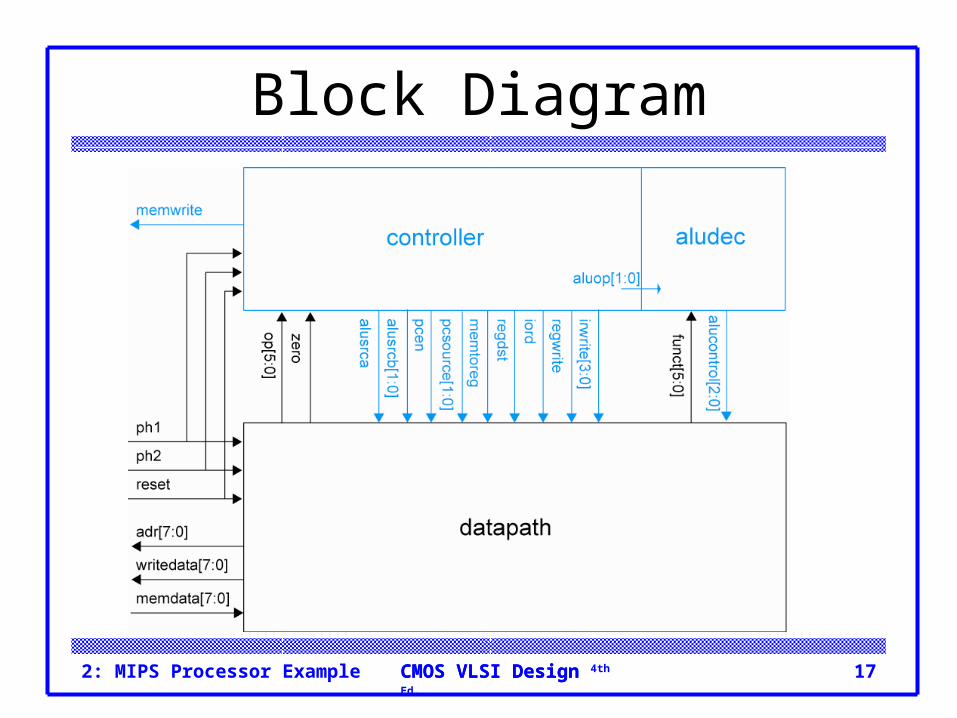
Block Diagram
2: MIPS Processor Example 18CMOS VLSI DesignCMOS VLSI Design 4th Ed.
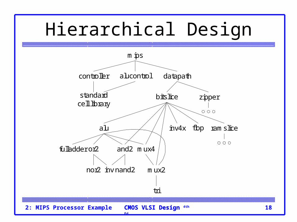
Hierarchical Designmips
controller alucontrol datapath
standardcell library
bitslice zipper
alu
and2
flopinv4x
mux2
mux4
ramslice
fulladder
nand2nor2
or2
inv
tri
2: MIPS Processor Example 19CMOS VLSI DesignCMOS VLSI Design 4th Ed.
HDLs Hardware Description Languages
– Widely used in logic design– Verilog and VHDL
Describe hardware using code– Document logic functions– Simulate logic before building– Synthesize code into gates and layout
• Requires a library of standard cells
2: MIPS Processor Example 20CMOS VLSI DesignCMOS VLSI Design 4th Ed.
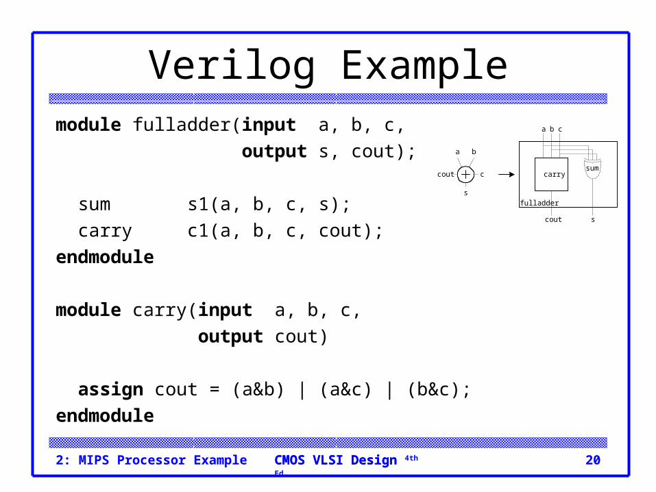
Verilog Examplemodule fulladder(input a, b, c,
output s, cout);
sum s1(a, b, c, s);
carry c1(a, b, c, cout);
endmodule
module carry(input a, b, c,
output cout)
assign cout = (a&b) | (a&c) | (b&c);
endmodule
a b
c
s
cout carrysum
s
a b c
cout
fulladder
2: MIPS Processor Example 21CMOS VLSI DesignCMOS VLSI Design 4th Ed.
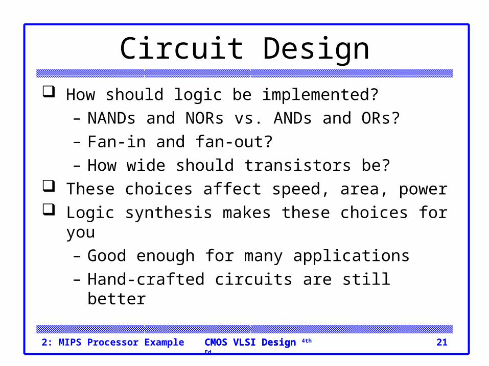
Circuit Design How should logic be implemented?
– NANDs and NORs vs. ANDs and ORs?– Fan-in and fan-out?– How wide should transistors be?
These choices affect speed, area, power Logic synthesis makes these choices for you
– Good enough for many applications– Hand-crafted circuits are still better
2: MIPS Processor Example 22CMOS VLSI DesignCMOS VLSI Design 4th Ed.
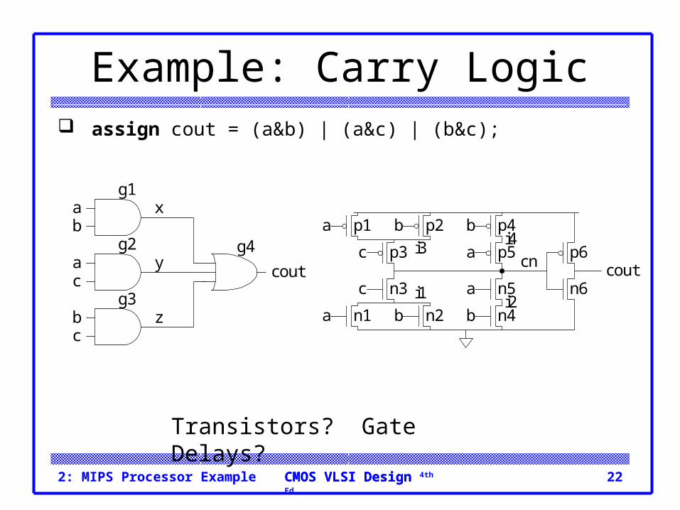
Example: Carry Logic assign cout = (a&b) | (a&c) | (b&c);
ab
ac
bc
cout
x
y
z
g1
g2
g3
g4
Transistors? Gate Delays?
a b
c
c
a b
b
a
a
b
coutcn
n1 n2
n3
n4
n5 n6
p6p5
p4
p3
p2p1
i1
i3
i2
i4
2: MIPS Processor Example 23CMOS VLSI DesignCMOS VLSI Design 4th Ed.
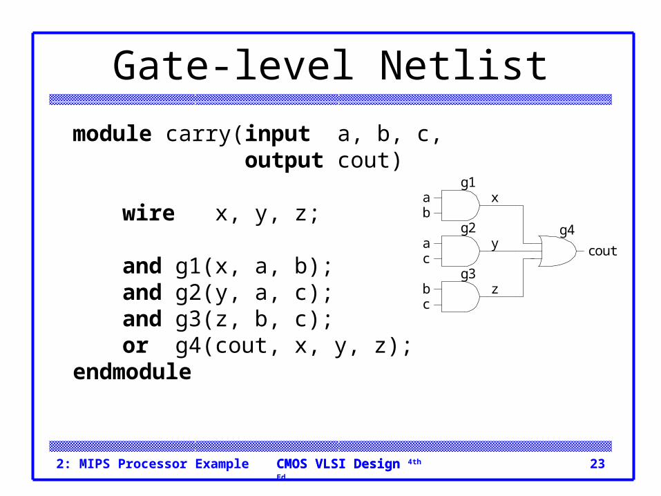
Gate-level Netlist
module carry(input a, b, c, output cout)
wire x, y, z;
and g1(x, a, b);and g2(y, a, c);and g3(z, b, c);or g4(cout, x, y, z);
endmodule
ab
ac
bc
cout
x
y
z
g1
g2
g3
g4
2: MIPS Processor Example 24CMOS VLSI DesignCMOS VLSI Design 4th Ed.
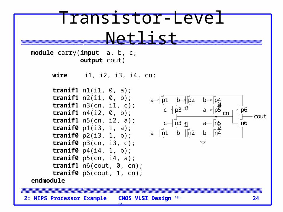
Transistor-Level Netlist
a b
c
c
a b
b
a
a
b
coutcn
n1 n2
n3
n4
n5 n6
p6p5
p4
p3
p2p1
i1
i3
i2
i4
module carry(input a, b, c, output cout)
wire i1, i2, i3, i4, cn;
tranif1 n1(i1, 0, a);tranif1 n2(i1, 0, b);tranif1 n3(cn, i1, c);tranif1 n4(i2, 0, b);tranif1 n5(cn, i2, a);tranif0 p1(i3, 1, a);tranif0 p2(i3, 1, b);tranif0 p3(cn, i3, c);tranif0 p4(i4, 1, b);tranif0 p5(cn, i4, a);tranif1 n6(cout, 0, cn);tranif0 p6(cout, 1, cn);
endmodule
2: MIPS Processor Example 25CMOS VLSI DesignCMOS VLSI Design 4th Ed.
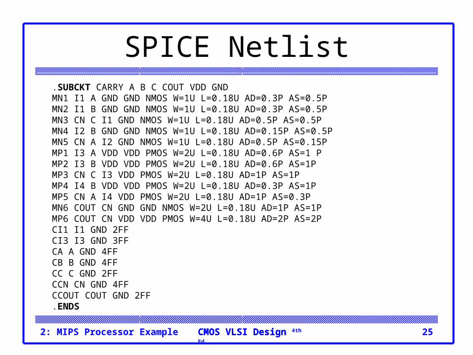
SPICE Netlist.SUBCKT CARRY A B C COUT VDD GNDMN1 I1 A GND GND NMOS W=1U L=0.18U AD=0.3P AS=0.5PMN2 I1 B GND GND NMOS W=1U L=0.18U AD=0.3P AS=0.5PMN3 CN C I1 GND NMOS W=1U L=0.18U AD=0.5P AS=0.5PMN4 I2 B GND GND NMOS W=1U L=0.18U AD=0.15P AS=0.5PMN5 CN A I2 GND NMOS W=1U L=0.18U AD=0.5P AS=0.15PMP1 I3 A VDD VDD PMOS W=2U L=0.18U AD=0.6P AS=1 PMP2 I3 B VDD VDD PMOS W=2U L=0.18U AD=0.6P AS=1PMP3 CN C I3 VDD PMOS W=2U L=0.18U AD=1P AS=1PMP4 I4 B VDD VDD PMOS W=2U L=0.18U AD=0.3P AS=1PMP5 CN A I4 VDD PMOS W=2U L=0.18U AD=1P AS=0.3PMN6 COUT CN GND GND NMOS W=2U L=0.18U AD=1P AS=1PMP6 COUT CN VDD VDD PMOS W=4U L=0.18U AD=2P AS=2PCI1 I1 GND 2FFCI3 I3 GND 3FFCA A GND 4FFCB B GND 4FFCC C GND 2FFCCN CN GND 4FFCCOUT COUT GND 2FF.ENDS
2: MIPS Processor Example 26CMOS VLSI DesignCMOS VLSI Design 4th Ed.
Physical Design Floorplan Standard cells
– Place & route Datapaths
– Slice planning Area estimation
2: MIPS Processor Example 27CMOS VLSI DesignCMOS VLSI Design 4th Ed.
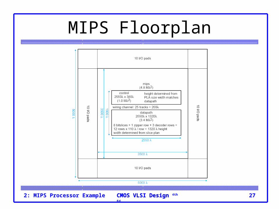
MIPS Floorplan
2: MIPS Processor Example 28CMOS VLSI DesignCMOS VLSI Design 4th Ed.
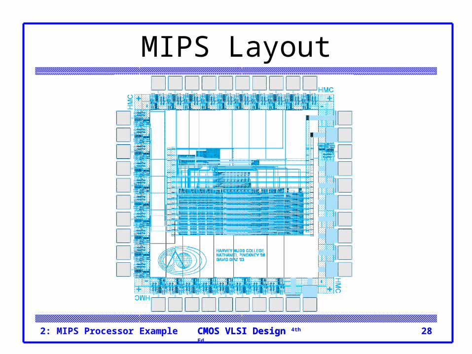
MIPS Layout

2: MIPS Processor Example 29CMOS VLSI DesignCMOS VLSI Design 4th Ed.
Standard Cells Uniform cell height Uniform well height M1 VDD and GND rails
M2 Access to I/Os Well / substrate taps Exploits regularity
2: MIPS Processor Example 30CMOS VLSI DesignCMOS VLSI Design 4th Ed.
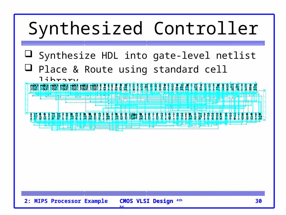
Synthesized Controller Synthesize HDL into gate-level netlist Place & Route using standard cell library
2: MIPS Processor Example 31CMOS VLSI DesignCMOS VLSI Design 4th Ed.
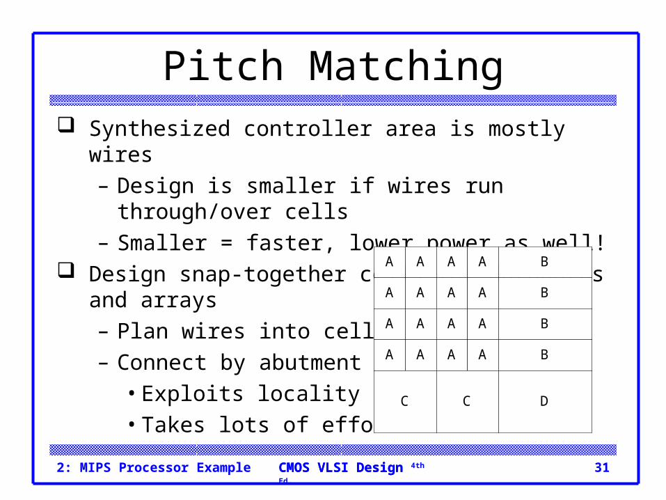
Pitch Matching Synthesized controller area is mostly wires
– Design is smaller if wires run through/over cells– Smaller = faster, lower power as well!
Design snap-together cells for datapaths and arrays– Plan wires into cells– Connect by abutment
• Exploits locality• Takes lots of effort
A A A A
A A A A
A A A A
A A A A
B
B
B
B
C C D
2: MIPS Processor Example 32CMOS VLSI DesignCMOS VLSI Design 4th Ed.
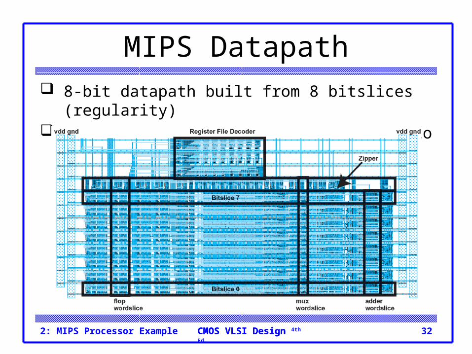
MIPS Datapath 8-bit datapath built from 8 bitslices (regularity) Zipper at top drives control signals to datapath
2: MIPS Processor Example 33CMOS VLSI DesignCMOS VLSI Design 4th Ed.
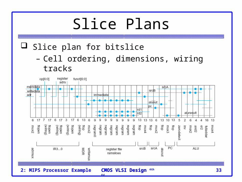
Slice Plans Slice plan for bitslice
– Cell ordering, dimensions, wiring tracks– Arrange cells for wiring locality
2: MIPS Processor Example 34CMOS VLSI DesignCMOS VLSI Design 4th Ed.
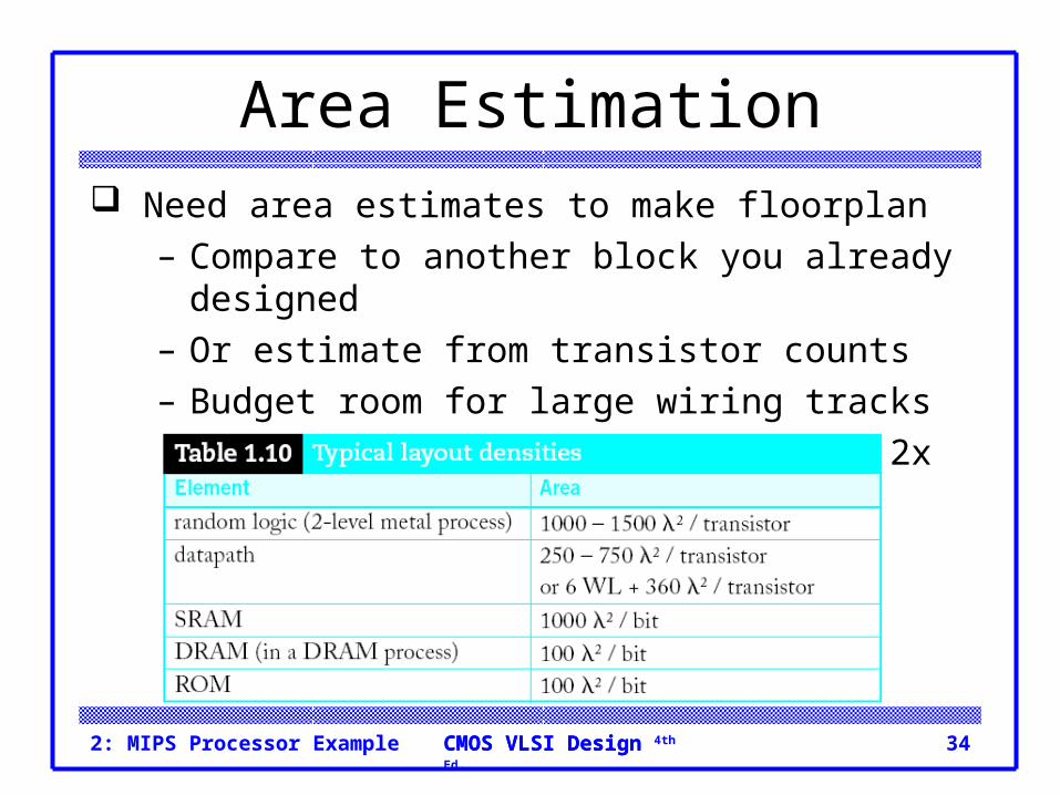
Area Estimation Need area estimates to make floorplan
– Compare to another block you already designed– Or estimate from transistor counts– Budget room for large wiring tracks– Your mileage may vary; derate by 2x for class.
2: MIPS Processor Example 35CMOS VLSI DesignCMOS VLSI Design 4th Ed.
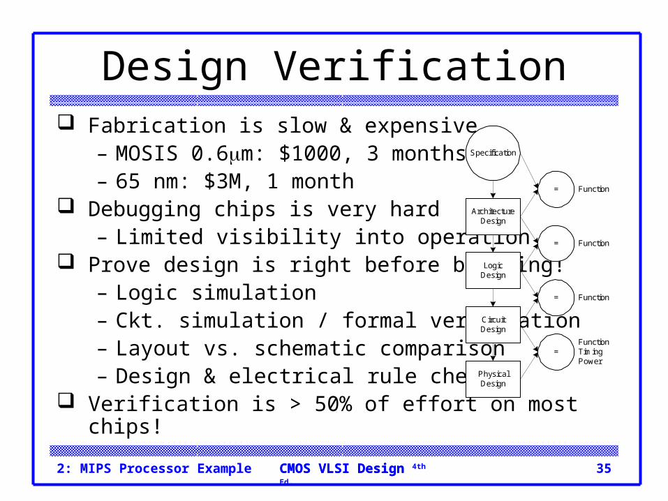
Design Verification Fabrication is slow & expensive
– MOSIS 0.6m: $1000, 3 months– 65 nm: $3M, 1 month
Debugging chips is very hard– Limited visibility into operation
Prove design is right before building!– Logic simulation– Ckt. simulation / formal verification– Layout vs. schematic comparison– Design & electrical rule checks
Verification is > 50% of effort on most chips!
Specification
ArchitectureDesign
LogicDesign
CircuitDesign
PhysicalDesign
=
=
=
=
Function
Function
Function
FunctionTimingPower
2: MIPS Processor Example 36CMOS VLSI DesignCMOS VLSI Design 4th Ed.
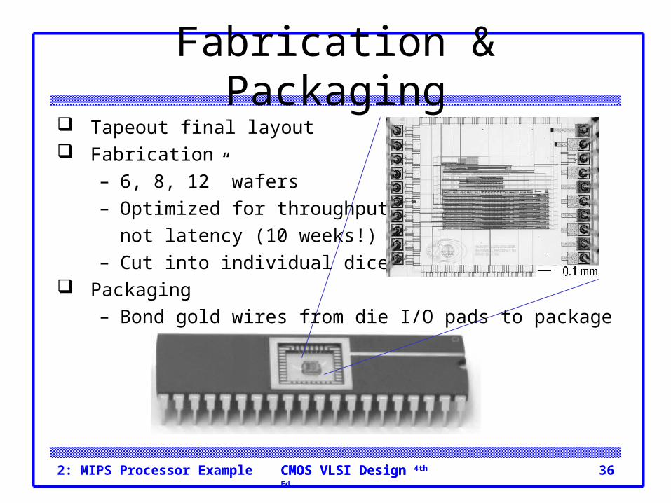
Fabrication & Packaging Tapeout final layout Fabrication
– 6, 8, 12” wafers– Optimized for throughput,
not latency (10 weeks!)– Cut into individual dice
Packaging– Bond gold wires from die I/O pads to package
2: MIPS Processor Example 37CMOS VLSI DesignCMOS VLSI Design 4th Ed.
Testing Test that chip operates
– Design errors– Manufacturing errors
A single dust particle or wafer defect kills a die– Yields from 90% to < 10%– Depends on die size, maturity of process– Test each part before shipping to customer
2: MIPS Processor Example 38CMOS VLSI DesignCMOS VLSI Design 4th Ed.
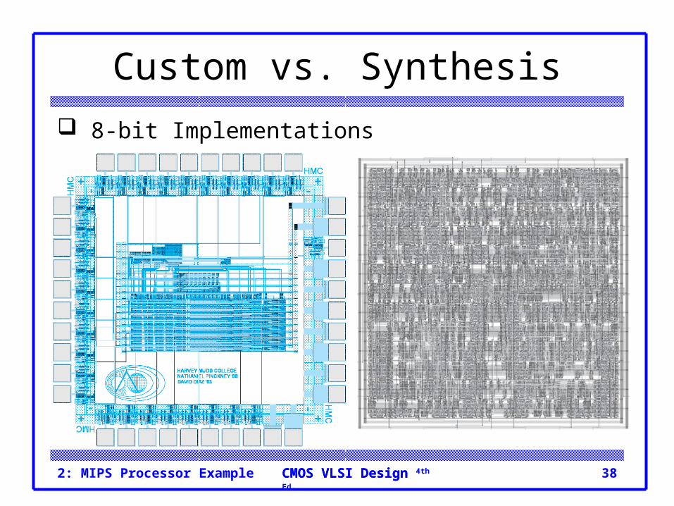
Custom vs. Synthesis
8-bit Implementations
2: MIPS Processor Example 39CMOS VLSI DesignCMOS VLSI Design 4th Ed.
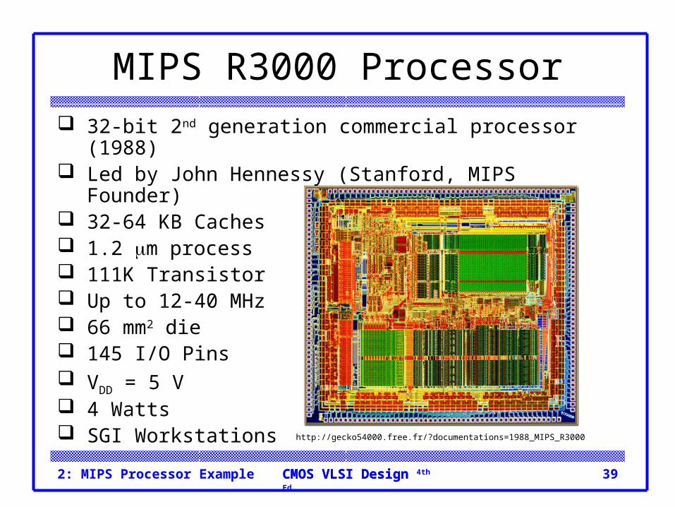
MIPS R3000 Processor 32-bit 2nd generation commercial processor (1988) Led by John Hennessy (Stanford, MIPS Founder) 32-64 KB Caches 1.2 m process 111K Transistor Up to 12-40 MHz 66 mm2 die 145 I/O Pins VDD = 5 V 4 Watts SGI Workstations http://gecko54000.free.fr/?documentations=1988_MIPS_R3000