Embed Size (px)
Citation preview

Introduction toCMOS VLSI
Design
Lecture 2: MIPS Processor Example
David Harris
Harvey Mudd CollegeSpring 2004

2: MIPS Processor Example Slide 2CMOS VLSI Design
Outlineq Design Partitioningq MIPS Processor Example
– Architecture– Microarchitecture– Logic Design– Circuit Design– Physical Design
q Fabrication, Packaging, Testing

2: MIPS Processor Example Slide 3CMOS VLSI Design
Activity 2q Sketch a stick diagram for a 4-input NOR gate

2: MIPS Processor Example Slide 5CMOS VLSI Design
Coping with Complexityq How to design System-on-Chip?
– Many millions (soon billions!) of transistors– Tens to hundreds of engineers
q Structured Designq Design Partitioning

2: MIPS Processor Example Slide 6CMOS VLSI Design
Structured Designq Hierarchy: Divide and Conquer
– Recursively system into modulesq Regularity
– Reuse modules wherever possible– Ex: Standard cell library
q Modularity: well-formed interfaces– Allows modules to be treated as black boxes
q Locality– Physical and temporal
2: MIPS Processor Example Slide 7CMOS VLSI Design
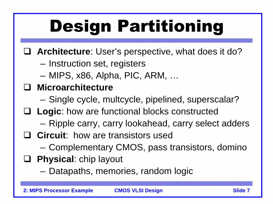
Design Partitioningq Architecture: User’s perspective, what does it do?
– Instruction set, registers– MIPS, x86, Alpha, PIC, ARM, …
q Microarchitecture– Single cycle, multcycle, pipelined, superscalar?
q Logic: how are functional blocks constructed– Ripple carry, carry lookahead, carry select adders
q Circuit: how are transistors used– Complementary CMOS, pass transistors, domino
q Physical: chip layout– Datapaths, memories, random logic

2: MIPS Processor Example Slide 8CMOS VLSI Design
Gajski Y-Chart

2: MIPS Processor Example Slide 9CMOS VLSI Design
MIPS Architectureq Example: subset of MIPS processor architecture
– Drawn from Patterson & Hennessyq MIPS is a 32-bit architecture with 32 registers
– Consider 8-bit subset using 8-bit datapath– Only implement 8 registers ($0 - $7)– $0 hardwired to 00000000– 8-bit program counter
q You’ll build this processor in the labs– Illustrate the key concepts in VLSI design

2: MIPS Processor Example Slide 10CMOS VLSI Design
Instruction Set

2: MIPS Processor Example Slide 11CMOS VLSI Design
Instruction Encodingq 32-bit instruction encoding
– Requires four cycles to fetch on 8-bit datapath
format example encoding
R
I
J
0 ra rb rd 0 funct
op
op
ra rb imm
6
6
6
65 5 5 5
5 5 16
26
add $rd, $ra, $rb
beq $ra, $rb, imm
j dest dest
2: MIPS Processor Example Slide 12CMOS VLSI Design
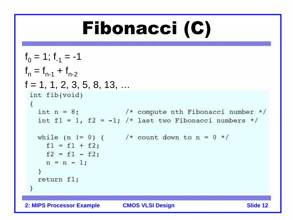
Fibonacci (C)f0 = 1; f-1 = -1fn = fn-1 + fn-2
f = 1, 1, 2, 3, 5, 8, 13, …

2: MIPS Processor Example Slide 13CMOS VLSI Design
Fibonacci (Assembly)q 1st statement: n = 8q How do we translate this to assembly?

2: MIPS Processor Example Slide 14CMOS VLSI Design
Fibonacci (Assembly)

2: MIPS Processor Example Slide 15CMOS VLSI Design
Fibonacci (Binary)q 1st statement: addi $3, $0, 8q How do we translate this to machine language?
– Hint: use instruction encodings below
format example encoding
R
I
J
0 ra rb rd 0 funct
op
op
ra rb imm
6
6
6
65 5 5 5
5 5 16
26
add $rd, $ra, $rb
beq $ra, $rb, imm
j dest dest

2: MIPS Processor Example Slide 16CMOS VLSI Design
Fibonacci (Binary)q Machine language program
2: MIPS Processor Example Slide 17CMOS VLSI Design
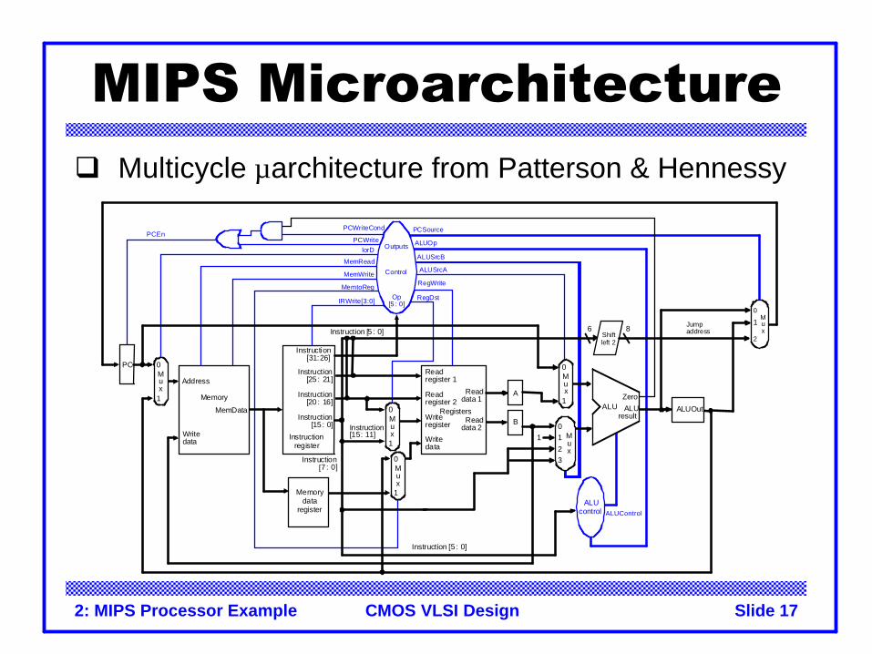
MIPS Microarchitectureq Multicycle µarchitecture from Patterson & Hennessy
PCMux
0
1
RegistersWriteregister
Writedata
Readdata 1
Readdata 2
Readregister 1
Readregister 2
Instruction[15: 11]
Mux
0
1
Mux
0
1
1
Instruction[7 : 0]
Instruction[25 : 21]
Instruction[20 : 16]
Instruction[15 : 0]
Instructionregister
ALUcontrol
ALUresult
ALUZero
Memorydata
register
A
B
IorD
MemRead
MemWrite
MemtoReg
PCWriteCond
PCWrite
IRWrite[3:0]
ALUOp
ALUSrcB
ALUSrcA
RegDst
PCSource
RegWrite
Control
Outputs
Op[5 : 0]
Instruction[31:26]
Instruction [5 : 0]
Mux
0
2
JumpaddressInstruction [5 : 0] 6 8
Shiftleft 2
1
1 Mux
0
32
Mux
0
1ALUOut
Memory
MemData
Writedata
Address
PCEn
ALUControl

2: MIPS Processor Example Slide 18CMOS VLSI Design
Multicycle Controller
PCWritePCSource = 10
ALUSrcA = 1ALUSrcB = 00ALUOp = 01PCWriteCond
PCSource = 01
ALUSrcA =1ALUSrcB = 00ALUOp= 10
RegDst = 1RegWrite
MemtoReg = 0
MemWriteIorD = 1
MemReadIorD = 1
ALUSrcA = 1ALUSrcB = 10ALUOp = 00
RegDst = 0RegWrite
MemtoReg=1
ALUSrcA = 0ALUSrcB = 11ALUOp = 00
MemReadALUSrcA = 0
IorD = 0IRWrite3
ALUSrcB = 01ALUOp = 00
PCWritePCSource = 00
Instruction fetch
Instruction decode/register fetch
Jumpcompletion
BranchcompletionExecution
Memory addresscomputation
Memoryaccess
Memoryaccess R-type completion
Write-back step
(Op = 'L B ') or (Op = 'SB ') (Op = R-type)
(Op
='B
EQ')
(Op
='J
')
(Op=
'SB')
(Op
='L
B')
7
0
4
121195
1086
Reset
MemReadALUSrcA = 0
IorD = 0IRWrite2
ALUSrcB = 01ALUOp = 00
PCWritePCSource = 00
1MemRead
ALUSrcA = 0IorD = 0IRWrite1
ALUSrcB = 01ALUOp = 00
PCWritePCSource = 00
2MemRead
ALUSrcA = 0IorD = 0IRWrite0
ALUSrcB = 01ALUOp = 00
PCWritePCSource = 00
3

2: MIPS Processor Example Slide 19CMOS VLSI Design
Logic Designq Start at top level
– Hierarchically decompose MIPS into unitsq Top-level interface
reset
ph1
ph2
crystaloscillator
2-phaseclockgenerator MIPS
processor adr
writedata
memdata
externalmemory
memreadmemwrite
8
8
8

2: MIPS Processor Example Slide 20CMOS VLSI Design
Block Diagram
datapath
controlleralucontrol
ph1
ph2
reset
memdata[7:0]
writedata[7:0]
adr[7:0]
memread
memwrite
op[5:0]
zero
pcen
regwrite
irwrite[3:0]
mem
toreg
iord
pcsource[1:0]
alusrcb[1:0]
alusrca
aluop[1:0]
regdst
funct[5:0]
alucontrol[2:0]
PCMux
0
1
R eg is tersWritereg ister
Writeda ta
Readda ta1
Readda ta2
Readreg ister 1
Readreg ister 2
Ins truc tion[15 : 11]
Mux
0
1
Mux
0
1
1
Ins truc tion[7 : 0 ]
Instruction[25 : 21 ]
Instruction[20 : 16 ]
Instruction[15 :0 ]
Ins truc tionregiste r
ALUc on trol
ALUresu l t
ALUZero
Memorydata
registe r
A
B
Io rD
MemRe ad
MemW rite
Me mto Reg
PCW riteCo nd
PCW ri te
IRW rite [ 3 : 0 ]
ALUOp
AL USrc B
AL USrcA
RegDs t
PCSo urce
Reg Wri te
Cont rol
O utpu ts
Op[5: 0]
Ins truction[31 :26 ]
Ins truction [5 :0 ]
Mux
0
2
J umpa dd re ssInstruction [5 : 0] 6 8
Shi f tle ft 2
1
1 Mux
0
32
Mux
0
1ALUOut
M em ory
MemData
Wri teda ta
Address
PCEn
A L U C o n t r o l

2: MIPS Processor Example Slide 21CMOS VLSI Design
Hierarchical Designmips
controller alucontrol datapath
standardcell library
bitslice zipper
alu
and2
flopinv4x
mux2
mux4
ramslice
fulladder
nand2nor2
or2
inv
tri

2: MIPS Processor Example Slide 22CMOS VLSI Design
HDLsq Hardware Description Languages
– Widely used in logic design– Verilog and VHDL
q Describe hardware using code– Document logic functions– Simulate logic before building– Synthesize code into gates and layout
• Requires a library of standard cells

2: MIPS Processor Example Slide 23CMOS VLSI Design
Verilog Examplemodule fulladder(input a, b, c,
output s, cout);
sum s1(a, b, c, s);carry c1(a, b, c, cout);
endmodule
module carry(input a, b, c, output cout)
assign cout = (a&b) | (a&c) | (b&c);endmodule
a b
c
s
cout carrysum
s
a b c
cout
fulladder

2: MIPS Processor Example Slide 24CMOS VLSI Design
Circuit Designq How should logic be implemented?
– NANDs and NORs vs. ANDs and ORs?– Fan-in and fan-out?– How wide should transistors be?
q These choices affect speed, area, powerq Logic synthesis makes these choices for you
– Good enough for many applications– Hand-crafted circuits are still better

2: MIPS Processor Example Slide 25CMOS VLSI Design
Example: Carry Logicq assign cout = (a&b) | (a&c) | (b&c);
Transistors? Gate Delays?

2: MIPS Processor Example Slide 28CMOS VLSI Design
Gate-level Netlistmodule carry(input a, b, c,
output cout)
wire x, y, z;
and g1(x, a, b);and g2(y, a, c);and g3(z, b, c);or g4(cout, x, y, z);
endmodule
ab
ac
bc
cout
x
y
z
g1
g2
g3
g4

2: MIPS Processor Example Slide 29CMOS VLSI Design
Transistor-Level Netlist
a b
c
c
a b
b
a
a
b
coutcn
n1 n2
n3
n4
n5 n6
p6p5
p4
p3
p2p1
i1
i3
i2
i4
module carry(input a, b, c, output cout)
wire i1, i2, i3, i4, cn;
tranif1 n1(i1, 0, a);tranif1 n2(i1, 0, b);tranif1 n3(cn, i1, c);tranif1 n4(i2, 0, b);tranif1 n5(cn, i2, a);tranif0 p1(i3, 1, a);tranif0 p2(i3, 1, b);tranif0 p3(cn, i3, c);tranif0 p4(i4, 1, b);tranif0 p5(cn, i4, a);tranif1 n6(cout, 0, cn);tranif0 p6(cout, 1, cn);
endmodule
2: MIPS Processor Example Slide 30CMOS VLSI Design
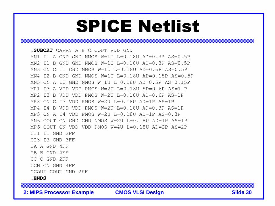
SPICE Netlist.SUBCKT CARRY A B C COUT VDD GNDMN1 I1 A GND GND NMOS W=1U L=0.18U AD=0.3P AS=0.5PMN2 I1 B GND GND NMOS W=1U L=0.18U AD=0.3P AS=0.5PMN3 CN C I1 GND NMOS W=1U L=0.18U AD=0.5P AS=0.5PMN4 I2 B GND GND NMOS W=1U L=0.18U AD=0.15P AS=0.5PMN5 CN A I2 GND NMOS W=1U L=0.18U AD=0.5P AS=0.15PMP1 I3 A VDD VDD PMOS W=2U L=0.18U AD=0.6P AS=1 PMP2 I3 B VDD VDD PMOS W=2U L=0.18U AD=0.6P AS=1PMP3 CN C I3 VDD PMOS W=2U L=0.18U AD=1P AS=1PMP4 I4 B VDD VDD PMOS W=2U L=0.18U AD=0.3P AS=1PMP5 CN A I4 VDD PMOS W=2U L=0.18U AD=1P AS=0.3PMN6 COUT CN GND GND NMOS W=2U L=0.18U AD=1P AS=1PMP6 COUT CN VDD VDD PMOS W=4U L=0.18U AD=2P AS=2PCI1 I1 GND 2FFCI3 I3 GND 3FFCA A GND 4FFCB B GND 4FFCC C GND 2FFCCN CN GND 4FFCCOUT COUT GND 2FF.ENDS

2: MIPS Processor Example Slide 31CMOS VLSI Design
Physical Designq Floorplanq Standard cells
– Place & routeq Datapaths
– Slice planningq Area estimation

2: MIPS Processor Example Slide 32CMOS VLSI Design
MIPS Floorplan
datapath2700 λ x 1050 λ
(2.8 Mλ2)
alucontrol200 λ x 100 λ
(20 kλ2)
zipper 2700 λ x 250 λ
2700 λ
1690 λ
wiring channel: 30 tracks = 240 λ
mips(4.6 Mλ2)
bitslice 2700 λ x 100 λ
control1500 λ x 400 λ
(0.6 Mλ2)
3500 λ
3500 λ
5000λ
5000 λ
10 I/O pads
10 I/O pads
10 I/O pads
10 I/O pads

2: MIPS Processor Example Slide 33CMOS VLSI Design
MIPS Layout

2: MIPS Processor Example Slide 34CMOS VLSI Design
Standard Cellsq Uniform cell heightq Uniform well heightq M1 VDD and GND railsq M2 Access to I/Osq Well / substrate tapsq Exploits regularity

2: MIPS Processor Example Slide 35CMOS VLSI Design
Synthesized Controllerq Synthesize HDL into gate-level netlistq Place & Route using standard cell library

2: MIPS Processor Example Slide 36CMOS VLSI Design
Pitch Matchingq Synthesized controller area is mostly wires
– Design is smaller if wires run through/over cells– Smaller = faster, lower power as well!
q Design snap-together cells for datapaths and arrays– Plan wires into cells– Connect by abutment
• Exploits locality• Takes lots of effort
A A A A
A A A A
A A A A
A A A A
B
B
B
B
C C D

2: MIPS Processor Example Slide 37CMOS VLSI Design
MIPS Datapathq 8-bit datapath built from 8 bitslices (regularity)q Zipper at top drives control signals to datapath

2: MIPS Processor Example Slide 38CMOS VLSI Design
Slice Plansq Slice plan for bitslice
– Cell ordering, dimensions, wiring tracks

2: MIPS Processor Example Slide 39CMOS VLSI Design
MIPS ALUq Arithmetic / Logic Unit is part of bitslice

2: MIPS Processor Example Slide 40CMOS VLSI Design
Area Estimationq Need area estimates to make floorplan
– Compare to another block you already designed– Or estimate from transistor counts– Budget room for large wiring tracks– Your mileage may vary!

2: MIPS Processor Example Slide 41CMOS VLSI Design
Design Verificationq Fabrication is slow & expensive
– MOSIS 0.6µm: $1000, 3 months– State of art: $1M, 1 month
q Debugging chips is very hard– Limited visibility into operation
q Prove design is right before building!– Logic simulation– Ckt. simulation / formal verification– Layout vs. schematic comparison– Design & electrical rule checks
q Verification is > 50% of effort on most chips!
Specification
ArchitectureDesign
LogicDesign
CircuitDesign
PhysicalDesign
=
=
=
=
Function
Function
Function
FunctionTimingPower

2: MIPS Processor Example Slide 42CMOS VLSI Design
Fabrication & Packagingq Tapeout final layoutq Fabrication
– 6, 8, 12” wafers– Optimized for throughput, not latency (10 weeks!)– Cut into individual dice
q Packaging– Bond gold wires from die I/O pads to package

2: MIPS Processor Example Slide 43CMOS VLSI Design
Testingq Test that chip operates
– Design errors– Manufacturing errors
q A single dust particle or wafer defect kills a die– Yields from 90% to < 10%– Depends on die size, maturity of process– Test each part before shipping to customer