Embed Size (px)
Citation preview

Ordering number : ENN6928
62901RM (OT) No. 6928-1/34
OverviewThe LC75411ES and 75411WS are electronic volumecontrollers that enable control of volume, balance, fader,bass/treble, loudness, input switching, and input gainusing only a small number of external components.
Functions• Volume: 0 dB to –79.5 dB in 0.5-dB steps, and –∞ (161
positions) Balance function with separate L/Rcontrol
• Fader: rear output or front output can be attenuatedacross 16 positions (in 1-dB steps from 0 dB to–2 dB, 2-dB steps from –2 dB to 20 dB, 10-dBsteps from –20 dB to –30 dB, and –45 dB, –60 dB, –∞)
• Bass/treble: Both bass and treble can be controlled in 1-dB steps from 0 dB to ±6 dB, and in 2-dBsteps from ±8 dB to ±12 dB.
• Input gain: 0 dB to +18.75 dB (1.25-dB steps)amplification is possible for the input signal.
• Input switching: four input signals can be selected forLeft and for Right
• Loudness: A tap is output from the –32 dB position of a2 dB step volume control resistor ladder. A loudness function can be implemented byconnecting an external RC circuit.
Features• On-chip buffer amplifier cuts down number of external
components• Low switching noise generated by on-chip switch
through use of silicon gate CMOS process, for lowswitching noise when there is no signal
• Low switching noise when there is a signal due to useof on-chip zero-cross switching circuit
• On-chip 1/2 VDD reference voltage circuit• Controls performed with serial input (CCB)
LC75411ES, 75411WS
SANYO Electric Co.,Ltd. Semiconductor CompanyTOKYO OFFICE Tokyo Bldg., 1-10, 1 Chome, Ueno, Taito-ku, TOKYO, 110-8534 JAPAN
Electronic Volume Controller for Car Audio Systems
CMOS IC
Any and all SANYO products described or contained herein do not have specifications that can handleapplications that require extremely high levels of reliability, such as life-support systems, aircraft’scontrol systems, or other applications whose failure can be reasonably expected to result in seriousphysical and/or material damage. Consult with your SANYO representative nearest you before usingany SANYO products described or contained herein in such applications.
SANYO assumes no responsibility for equipment failures that result from using products at values thatexceed, even momentarily, rated values (such as maximum ratings, operating condition ranges, or otherparameters) listed in products specifications of any and all SANYO products described or containedherein.
• CCB is a trademark of SANYO ELECTRIC CO., LTD.
• CCB is SANYO’s original bus format and all the busaddresses are controlled by SANYO.
No. 6928-2/33
LC75411ES, 75411WS
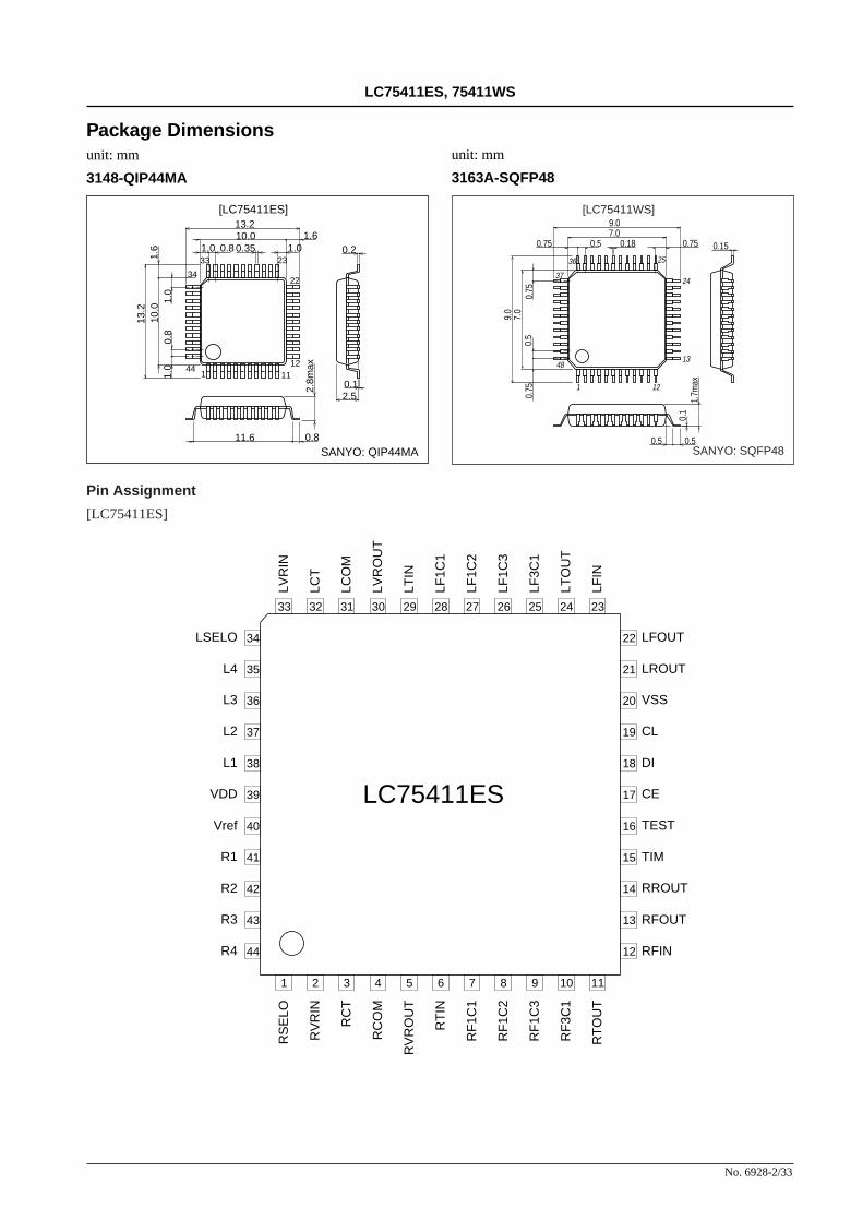
Package Dimensionsunit: mm
3148-QIP44MA
unit: mm
3163A-SQFP48
2.8m
ax
0.811.6
0.3510.013.2
1.0
1 1112
22
2333
34
44
1.01.6
0.8
2.5
0.2
0.1
10.0
13.2
1.0
1.0
1.6
0.8
SANYO: QIP44MA
[LC75411ES]
0.5
7.0
9.0
0.150.180.75 0.5 0.75
0.75
0.5
0.75
0.5
0.1
1 12
13
24
2536
37
48
7.09.0
1.7m
ax
SANYO: SQFP48
[LC75411WS]
Pin Assignment
[LC75411ES]
5 4 3 2 1
44
43
42
41
40
39
38
37
36
35
34
24 2526 27 28 29 30 33 32 31 23
16
15
14
13
12
11 10 9 8 7 6
22
21
20
19
18
17
LSELO
L4
L3
L2
L1
LC75411ESVDD
Vref
R1
R4
R3
R2
RS
ELO
RV
RIN
RC
T
RC
OM
RV
RO
UT
RT
IN
RF
1C1
RF
1C2
RF
1C3
RF
3C1
RT
OU
T
RFIN
RFOUT
RROUT
TIM
TEST
CE
DI
CL
VSS
LROUT
LFOUT
LFIN
LTO
UT
LF3C
1
LF1C
3
LF1C
2
LF1C
1
LTIN
LVR
OU
T
LCO
M
LVR
IN
LCT

No. 6928-3/33
LC75411ES, 75411WS
Equivalent Circuit Block Diagram
[LC75411ES]
DI
CE
CL
0.03
3µF
10µF
10µF
PA
L4
LFIN
Microcontroller
RFIN
RFOU
T
RROU
T
TIM
TEST
VD
D
CE
DI
CL
LROU
T
LFOU
T 22
24
23
LOGI
C CI
RCUI
T
ZERO
CROS
S DE
T
ZERO
CROS
S DE
T
CCB
INTE
RFAC
E
21
20
19
18
17
16
15
14
13
12
PA
VSS
10µF
PA
10µF
PA
25
26
27
28
29
11
10
9 8
7 6
35
36
37
38
39
40
41
42
43
44
L3 L2 L1
LVre
f VD
D
Vref
RVre
f
R1 R2 R3
1µF
× 4
R4
[TRE
BLE]
[TRE
BLE]
[B
ASS
fo=1
00Hz
]
0.1µF
0.1µF
2700pF
10µF
LF3C1
LTOUT
LF1C2
LF1C3
LF1C1
LTIN 10µF
CONT
ROL
CIRC
UIT
NO S
IGNA
L TI
MER
Mul
tiple
xer
Mul
tiple
xer [B
ASS
fo=1
00Hz
]
0.1µF
2700pF
10µF
RF3C1
RTOUT
RF1C2
RF1C3
RF1C1
RTIN
22µF
30
31
32
33
34
LVROUT
LVref
LCOM
LSELO
LVRIN
LCT 10µF
220p
F
1µF
0.1µ
F
68kΩ
4.7k
Ω LV
ref
RVref LVref
5 4
3 2
1
RVROUT
RVref
RCOM
RSELO
RVRIN
RCT
10µF
10µF
220p
F
1µF
0.1µ
F68kΩ
4.7k
Ω RV
ref
0.1µF

No. 6928-4/33
LC75411ES, 75411WS
Sample Application Circuit
[LC75411ES]
0.033µF
5 4 3 2 1
44
43
42
41
40
39
38
37
36
35
34
24 2526 27 28 29 30 33 32 31 23
16
15
14
13
12
11 10 9 8 7 6
22
21
20
19
18
17
4.7kΩ
4.7kΩ
68kΩ
68kΩ
220pF
220pF
2700pF
2700pF
0.1µF
0.1µF
0.1µF
0.1µF
0.1µF
0.1µF
10µF
10µF
10µF
Micro-controller
10µF
10µF
1µF
1µF
10µF10µF1µF
1µF
LSELO
L4
L3
L2
L1
VDD LC75411ESVDD
Vref
R1
R4
R3
R2
RSEL
O
RVRI
N
RCT
RCOM
RVRO
UT
RTIN
RF1C
1
RF1C
2
RF1C
3
RF3C
1
RTOU
T
RFIN
RFOUT
RROUT
TIM
TEST
CE
DI
PA
CL
DVSS
LROUT
LFOUT
LFIN
LTOU
T
LF3C
1
LF1C
3
LF1C
2
LF1C
1
LTIN
LVRO
UT
LCOM
LVRI
N
LCT
1µF
22µF
1µF
1µF
1µF
1µF
1µF
10µFPA
10µFPA
10µFPA

No. 6928-5/33
LC75411ES, 75411WS
Pin Assignment
[LC75411WS]
LC75411WS
48
47
46
45
44
43
42
41
40
39
38
L4
L3
L2
L1
NC
VDD
Vref
NC
R3
R2
R1
5 4 3 2 1 11 10 9 8 7 6
RS
ELO
RV
RIN
RC
T
RC
OM
RV
RO
UT
RT
IN
RF
1C1
RF
1C2
RF
1C3
RF
3C1
RT
OU
T
17
16
15
14
13
23
22
21
20
19
18
RFIN
RFOUT
RROUT
TIM
TEST
CE
DI
CL
VSS
LROUT
LFOUT
26 2728 29 30 31 32 35 34 33 25
NC
LTO
UT
LF3C
1
LF1C
3
LF1C
2
LF1C
1
LTIN
LVR
OU
T
LCO
M
LVR
IN
LCT
12
24
36
37
NC
LFIN
LSE
LO
R4

No. 6928-6/33
LC75411ES, 75411WS
Equivalent Circuit Block Diagram
[LC75411WS]
DI
CE
CL
0.03
3µF
10µF
10µF
PA
L4LF
IN
Microcontroller
RFIN
RFOU
T
RROU
T
TIM
TEST
VD
D
CE
DI
CL
LROU
T
LFOU
T 23
26
24
LOGI
C CI
RCUI
T
ZERO
CROS
S DE
T
Mul
tiple
xer
ZERO
CROS
S DE
T
CCB
INTE
RFAC
E
22
21
20
19
18
17
16
15
14
13
PA
VSS
10µF
PA
10µF
PA
27
28
29
30
31
11
10
9 8
7 6
37
38
39
40
42
43
45
46
47
48
L3 L2 NCL1
LVre
f VD
D
Vref
RVre
f
R1 R2 R3
1µF
× 4
NC R4
[TRE
BLE]
[TRE
BLE]
[B
ASS
fo=1
00Hz
]
0.1µF
0.1µF
2700pF
10µF
LF3C1
NC
LTOUT
LF1C2
LF1C3
LF1C1
LTIN 10µF
CONT
ROL
CIRC
UIT
NO S
IGNA
LTI
MER
Mul
tiple
xer
[BAS
S fo
=100
Hz]
0.1µF
0.1µF
2700pF
10µF
RF3C1
NC
RTOUT
RF1C2
RF1C3
RF1C1
RTIN
22µF
32
33
34
35
36
LVROUT
LVref
LCOM
LSELO
LVRIN
LCT 10µF
220p
F
1µF
0.1µ
F
68kΩ
4.7k
Ω LV
ref
RVref LVref
5 4
3 2
1
RVROUT
RVref
RCOM
RSELO
RVRIN
RCT
10µF
10µF
220p
F
1µF
0.1µ
F68kΩ
4.7k
Ω RV
ref
12
44
25
41

No. 6928-7/33
LC75411ES, 75411WS
Sample Application Circuit
[LC75411WS]
5 4 3 2 1
47
48
46
45
44
43
42
41
40
39
38
37
26 2728 29 30 31 32 35 36 34 33 25
17
16
15
14
13
12 11 10 9 8 7 6
24
23
22
21
20
19
18
4.7kΩ
4.7kΩ
68kΩ
68kΩ
220pF
220pF
2700pF
2700pF
0.1µF
0.1µF
0.1µF
0.1µF
0.1µF
0.1µF
10µF
10µF10µF
Micro-controller
10µF
10µF
1µF
1µF
10µF10µF1µF
1µF
L3
L2
L1
VDD
LC75411WSVDD
Vref
R3
NC
R2
R1
RSEL
O
RVRI
N NCRCT
RCOM
RVRO
UT
RTIN
RF1C
1
RF1C
2
RF1C
3
RF3C
1
RTOU
T
RFIN
RFOUT
RROUT
TIM
TEST
CE
DI
PA
CL
LFIN
VSS
LROUT
LFOUT
NC
LTOU
T
LF3C
1
LF1C
3
LF1C
2
LF1C
1
LTIN
LVRO
UT
LCOM
LVRI
N
LCT
LSEL
O
1µF
22µF
1µF
1µF
1µF
10µFPA
10µFPA
10µFPA
L41µF
R41µF
NC

No. 6928-8/33
LC75411ES, 75411WS
Parameter Symbol Conditions Ratings Unit
Maximum supply voltage VDD max VDD 11 V
Maximum input voltage VIN max All input pins VSS – 0.3 to VDD + 0.3 V
Allowable power dissipation Pd max Ta ≤ 85°C, when mounted on boardLC75411ES 600
mWLC75411WS 550
Operating temperature Topr –40 to +85 °C
Storage temperature Tstg –50 to +125 °C
SpecificationsAbsolute Maximum Ratings at Ta = 25°C, VSS = 0 V
Parameter Symbol ConditionsRatings
Unitmin typ max
Supply voltage VDD VDD 6.0 10.5 V
Input high-level voltage VIH CL, DI, CE, TEST 4.0 10.5 V
Input low-level voltage VIL CL, DI, CE, TEST VSS 1.0 V
Input amplitude voltage VIN VSS VDD Vp-p
Input pulse width TøW CL 1 µs
Setup time Tsetup CL, DI, CE 1 µs
Hold time Thold CL, DI, CE 1 µs
Operating frequency fopg CL 500 kHz
Allowable Operating Ranges at Ta = 25°C, VSS = 0 V
Parameter Symbol Pin Name ConditionsRatings
Unitmin typ max
[Input block]
Input resistance Rin L1 to L4, R1 to R4 25 50 100 kΩ
Minimum input gain Ginmin L1 to L4, R1 to R4 –1 0 +1 dB
Maximum input gain Ginmax +16.5 +18.75 +21 dB
Step setting error ATerr ±0.5 dB
L/R balance BAL ±0.5 dB
[Volume Block]
Input resistance Rvr LVRIN, RVRIN, loudness off 113 226 452 kΩ
Step setting error ATerr ±0.5 dB
L/R balance BAL ±0.5 dB
[Tone block]
Step setting error ATerr ±1.0 dB
Bass control range Gbass max. boost/cut ±9 ±12 ±15 dB
Treble control range Gtre max. boost/cut ±9 ±12 ±15 dB
L/R balance BAL ±0.5 dB
Electrical Characteristics at Ta = 25°C, VDD = 9 V, VSS = 0 V
Continued on next page.

No. 6928-9/33
LC75411ES, 75411WS
Parameter Symbol Pin Name ConditionsRatings
Unitmin typ max
[Fader Block]
Input resistance Rfed LFIN, RFIN 25 50 100 kΩ
0dB to –2dB ±0.5 dB
Step setting error ATerr–2dB to –20dB ±1 dB
–20dB to –30dB ±2 dB
–30dB to –60dB ±3 dB
L/R balance BAL ±0.5 dB
[General]
Total harmonic distortionTHD (1) VIN = –10dBV, f = 1 kHz 0.004 0.01 %
THD (2) VIN = –10dBV, f = 10 kHz 0.006 0.01 %
Input crosstalk CT VIN = 1Vrms, f = 1 kHz 80 88 dB
L/R crosstalk CT VIN = 1Vrms, f = 1 kHz 80 88 dB
Maximum attenuated output
Vomin (1) VIN = 1Vrms, f = 1 kHz 80 88 dB
Vomin (2)VIN = 1Vrms, f = 1 kHz
90 95 dBINMUTE, fader –∞
Output noise voltageVN (1) Flat overall, IHF-A filter 5 10 µV
VN (2) Flat overall, 20 to 20 kHzBPF 7 15 µV
Current drain IDD 33 40 mA
Input high-level current IIH CL, DI, CE, VIN = 9 V 10 µA
Input low-level current IIL CL, DI, CE, VIN = 0 V –10 µA
Maximum input voltage VCLTHD = 1%, RL = 10 kΩ
2.5 2.9 Vrmsflat overall, fIN = 1 kHz
Continued from preceding page.
Control Timing and Data Format
To control the LC75411ES and LC75411WS input specified serial data to the CE, CL, and DI pins.The data configuration consists of a total of 52 bits broken down into 8 address bits and 44 data bits.
CE
DI D43 D42 D41 D40 D39 D38 D5 D4 D3 D2 D0 D1 A3 A2 A1 A0 B3 B2 B1 B0
CL
1µsmin
1µsmin
1µs min ≤ TDEST
1µsmin
1µsmin
1µsmin
CE
DI
CL

Address code (B0 to A3)
The LC75411ES and 75411WS use 8-bit address code and can be used in common with ICs that support SANYO’s CCBserial bus.
Address Code
(LSB) (81HEX)
Control code allocation
Input Switching Control
No. 6928-10/33
LC75411ES, 75411WS
B0 B1 B2 B3 A0 A1 A2 A3
1 0 0 0 0 0 0 1
D0 D1 D2 Setting Setting
0 0 0 L1 (R1)
1 0 0 L2 (R2)
0 1 0 L3 (R3)
1 1 0 L4 (R4)
0 1 1For IC testing: Normally not used
1 1 1
D3 Bit for IC testing: Normally set to 0
Input Gain Control
D4 D5 D6 D7 Operation
0 0 0 0 0dB
1 0 0 0 +1.25dB
0 1 0 0 +2.50dB
1 1 0 0 +3.75dB
0 0 1 0 +5.00dB
1 0 1 0 +6.25dB
0 1 1 0 +7.50dB
1 1 1 0 +8.75dB
0 0 0 1 +10.0dB
1 0 0 1 +11.25dB
0 1 0 1 +12.5dB
1 1 0 1 +13.75dB
0 0 1 1 +15.0dB
1 0 1 1 +16.25dB
0 1 1 1 +17.5dB
1 1 1 1 +18.75dB

No. 6928-11/33
LC75411ES, 75411WS
Volume Control (0 to –20.5dB)
D8 D9 D10 D11 D12 D13 D14 D15 Operation
0 0 0 0 0 0 0 0 0dB
0 0 0 0 0 0 0 1 –0.5dB
1 0 0 0 0 0 0 0 –1dB
1 0 0 0 0 0 0 1 –1.5dB
0 1 0 0 0 0 0 0 –2dB
0 1 0 0 0 0 0 1 –2.5dB
1 1 0 0 0 0 0 0 –3dB
1 1 0 0 0 0 0 1 –3.5dB
0 0 1 0 0 0 0 0 –4dB
0 0 1 0 0 0 0 1 –4.5dB
1 0 1 0 0 0 0 0 –5dB
1 0 1 0 0 0 0 1 –5.5dB
0 1 1 0 0 0 0 0 –6dB
0 1 1 0 0 0 0 1 –6.5dB
1 1 1 0 0 0 0 0 –7dB
1 1 1 0 0 0 0 1 –7.5dB
0 0 0 1 0 0 0 0 –8dB
0 0 0 1 0 0 0 1 –8.5dB
1 0 0 1 0 0 0 0 –9dB
1 0 0 1 0 0 0 1 –9.5dB
0 1 0 1 0 0 0 0 –10dB
0 1 0 1 0 0 0 1 –10.5dB
1 1 0 1 0 0 0 0 –11dB
1 1 0 1 0 0 0 1 –11.5dB
0 0 1 1 0 0 0 0 –12dB
0 0 1 1 0 0 0 1 –12.5dB
1 0 1 1 0 0 0 0 –13dB
1 0 1 1 0 0 0 1 –13.5dB
0 1 1 1 0 0 0 0 –14dB
0 1 1 1 0 0 0 1 –14.5dB
1 1 1 1 0 0 0 0 –15dB
1 1 1 1 0 0 0 1 –15.5dB
0 0 0 0 1 0 0 0 –16dB
0 0 0 0 1 0 0 1 –16.5dB
1 0 0 0 1 0 0 0 –17dB
1 0 0 0 1 0 0 1 –17.5dB
0 1 0 0 1 0 0 0 –18dB
0 1 0 0 1 0 0 1 –18.5dB
1 1 0 0 1 0 0 0 –19dB
1 1 0 0 1 0 0 1 –19.5dB
0 0 1 0 1 0 0 0 –20dB
0 0 1 0 1 0 0 1 –20.5dB

No. 6928-12/33
LC75411ES, 75411WS
Volume Control (–21 to –40.5dB)
D8 D9 D10 D11 D12 D13 D14 D15 Operation
1 0 1 0 1 0 0 0 –21dB
1 0 1 0 1 0 0 1 –21.5dB
0 1 1 0 1 0 0 0 –22dB
0 1 1 0 1 0 0 1 –22.5dB
1 1 1 0 1 0 0 0 –23dB
1 1 1 0 1 0 0 1 –23.5dB
0 0 0 1 1 0 0 0 –24dB
0 0 0 1 1 0 0 1 –24.5dB
1 0 0 1 1 0 0 0 –25dB
1 0 0 1 1 0 0 1 –25.5dB
0 1 0 1 1 0 0 0 –26dB
0 1 0 1 1 0 0 1 –26.5dB
1 1 0 1 1 0 0 0 –27dB
1 1 0 1 1 0 0 1 –27.5dB
0 0 1 1 1 0 0 0 –28dB
0 0 1 1 1 0 0 1 –28.5dB
1 0 1 1 1 0 0 0 –29dB
1 0 1 1 1 0 0 1 –29.5dB
0 1 1 1 1 0 0 0 –30dB
0 1 1 1 1 0 0 1 –30.5dB
1 1 1 1 1 0 0 0 –31dB
1 1 1 1 1 0 0 1 –31.5dB
0 0 0 0 0 1 0 0 –32dB
0 0 0 0 0 1 0 1 –32.5dB
1 0 0 0 0 1 0 0 –33dB
1 0 0 0 0 1 0 1 –33.5dB
0 1 0 0 0 1 0 0 –34dB
0 1 0 0 0 1 0 1 –34.5dB
1 1 0 0 0 1 0 0 –35dB
1 1 0 0 0 1 0 1 –35.5dB
0 0 1 0 0 1 0 0 –36dB
0 0 1 0 0 1 0 1 –36.5dB
1 0 1 0 0 1 0 0 –37dB
1 0 1 0 0 1 0 1 –37.5dB
0 1 1 0 0 1 0 0 –38dB
0 1 1 0 0 1 0 1 –38.5dB
1 1 1 0 0 1 0 0 –39dB
1 1 1 0 0 1 0 1 –39.5dB
0 0 0 1 0 1 0 0 –40dB
0 0 0 1 0 1 0 1 –40.5dB

No. 6928-13/33
LC75411ES, 75411WS
Volume Control (–41 to –59.5dB)
D8 D9 D10 D11 D12 D13 D14 D15 Operation
1 0 0 1 0 1 0 0 –41dB
1 0 0 1 0 1 0 1 –41.5dB
0 1 0 1 0 1 0 0 –42dB
0 1 0 1 0 1 0 1 –42.5dB
1 1 0 1 0 1 0 0 –43dB
1 1 0 1 0 1 0 1 –43.5dB
0 0 1 1 0 1 0 0 –44dB
0 0 1 1 0 1 0 1 –44.5dB
1 0 1 1 0 1 0 0 –45dB
1 0 1 1 0 1 0 1 –45.5dB
0 1 1 1 0 1 0 0 –46dB
0 1 1 1 0 1 0 1 –46.5dB
1 1 1 1 0 1 0 0 –47dB
1 1 1 1 0 1 0 1 –47.5dB
0 0 0 0 1 1 0 0 –48dB
0 0 0 0 1 1 0 1 –48.5dB
1 0 0 0 1 1 0 0 –49dB
1 0 0 0 1 1 0 1 –49.5dB
0 1 0 0 1 1 0 0 –50dB
0 1 0 0 1 1 0 1 –50.5dB
1 1 0 0 1 1 0 0 –51dB
1 1 0 0 1 1 0 1 –51.5dB
0 0 1 0 1 1 0 0 –52dB
0 0 1 0 1 1 0 1 –52.5dB
1 0 1 0 1 1 0 0 –53dB
1 0 1 0 1 1 0 1 –53.5dB
0 1 1 0 1 1 0 0 –54dB
0 1 1 0 1 1 0 1 –54.5dB
1 1 1 0 1 1 0 0 –55dB
1 1 1 0 1 1 0 1 –55.5dB
0 0 0 1 1 1 0 0 –56dB
0 0 0 1 1 1 0 1 –56.5dB
1 0 0 1 1 1 0 0 –57dB
1 0 0 1 1 1 0 1 –57.5dB
0 1 0 1 1 1 0 0 –58dB
0 1 0 1 1 1 0 1 –58.5dB
1 1 0 1 1 1 0 0 –59dB
1 1 0 1 1 1 0 1 –59.5dB
No. 6928-14/33
LC75411ES, 75411WS
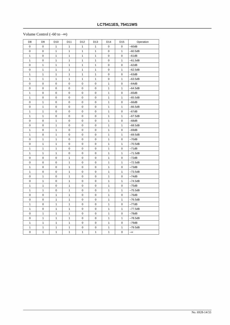
Volume Control (–60 to –∞)
D8 D9 D10 D11 D12 D13 D14 D15 Operation
0 0 1 1 1 1 0 0 –60dB
0 0 1 1 1 1 0 1 –60.5dB
1 0 1 1 1 1 0 0 –61dB
1 0 1 1 1 1 0 1 –61.5dB
0 1 1 1 1 1 0 0 –62dB
0 1 1 1 1 1 0 1 –62.5dB
1 1 1 1 1 1 0 0 –63dB
1 1 1 1 1 1 0 1 –63.5dB
0 0 0 0 0 0 1 0 –64dB
0 0 0 0 0 0 1 1 –64.5dB
1 0 0 0 0 0 1 0 –65dB
1 0 0 0 0 0 1 1 –65.5dB
0 1 0 0 0 0 1 0 –66dB
0 1 0 0 0 0 1 1 –66.5dB
1 1 0 0 0 0 1 0 –67dB
1 1 0 0 0 0 1 1 –67.5dB
0 0 1 0 0 0 1 0 –68dB
0 0 1 0 0 0 1 1 –68.5dB
1 0 1 0 0 0 1 0 –69dB
1 0 1 0 0 0 1 1 –69.5dB
0 1 1 0 0 0 1 0 –70dB
0 1 1 0 0 0 1 1 –70.5dB
1 1 1 0 0 0 1 0 –71dB
1 1 1 0 0 0 1 1 –71.5dB
0 0 0 1 0 0 1 0 –72dB
0 0 0 1 0 0 1 1 –72.5dB
1 0 0 1 0 0 1 0 –73dB
1 0 0 1 0 0 1 1 –73.5dB
0 1 0 1 0 0 1 0 –74dB
0 1 0 1 0 0 1 1 –74.5dB
1 1 0 1 0 0 1 0 –75dB
1 1 0 1 0 0 1 1 –75.5dB
0 0 1 1 0 0 1 0 –76dB
0 0 1 1 0 0 1 1 –76.5dB
1 0 1 1 0 0 1 0 –77dB
1 0 1 1 0 0 1 1 –77.5dB
0 1 1 1 0 0 1 0 –78dB
0 1 1 1 0 0 1 1 –78.5dB
1 1 1 1 0 0 1 0 –79dB
1 1 1 1 0 0 1 1 –79.5dB
0 1 1 1 1 1 1 0 –∞

No. 6928-15/33
LC75411ES, 75411WS
Tone Control
D16 D17 D18 D19 D40 Bass
D24 D25 D26 D27 D42 Treble
0 1 1 0 0 +12dB
1 0 1 0 0 +10dB
0 0 1 0 0 +8dB
1 1 0 0 0 +6dB
1 1 0 0 1 +5dB
0 1 0 0 0 +4dB
0 1 0 0 1 +3dB
1 0 0 0 0 +2dB
1 0 0 0 1 +1dB
0 0 0 0 0 0dB
1 0 0 1 1 –1dB
1 0 0 1 0 –2dB
0 1 0 1 1 –3dB
0 1 0 1 0 –4dB
1 1 0 1 1 –5dB
1 1 0 1 0 –6dB
0 0 1 1 0 –8dB
1 0 1 1 0 –10dB
0 1 1 1 0 –12dB
D20 D21 D22 D23 D41 Setting
0 0 0 0 0 Set to 0
Fader Volume Control
D28 D29 D30 D31 Operation
0 0 0 0 0dB
1 0 0 0 –1dB
0 1 0 0 –2dB
1 1 0 0 –4dB
0 0 1 0 –6dB
1 0 1 0 –8dB
0 1 1 0 –10dB
1 1 1 0 –12dB
0 0 0 1 –14dB
1 0 0 1 –16dB
0 1 0 1 –18dB
1 1 0 1 –20dB
0 0 1 1 –30dB
1 0 1 1 –45dB
0 1 1 1 –60dB
1 1 1 1 –∞
Channel Selection Control
D32 D33 Operation
0 0 Initial setting mode: Rapid charging
1 0 RCH
0 1 LCH
1 1 L/R simultaneously

No. 6928-16/33
LC75411ES, 75411WS
Fader Rear/Front Control
D34 Setting
0 Rear
1 Front
Loudness Control
D35 Setting
0 OFF
1 ON
Test Mode Control
D43 Setting
0 For IC testing. Always set to 0.
Zero-Cross Control
D36 D37 Setting
0 0 Data write through zero-cross detection
1 1 Zero-cross detection stopped (data write at falling edge of CE)
Zero-Cross Signal Detection Block Control
D38 D39 Setting
0 0 Selector
1 0 Volume
0 1 Tone
1 1 Fader

No. 6928-17/33
LC75411ES, 75411WS
Pin Functions
Pin NamePin No.
Function Equivalent circuitLC75411ES LC75411WS
• Single-end input pin
L1
L2
L3
L4
R1
R2
R3
R4
38
37
36
35
41
42
43
44
40
39
38
37
45
46
47
48
VDD
LVref RVref
• Input selector output pinsLSEL0
RSEL0
34
1
36
1
VDD
• 2-dB step volume input pins
• Perform input at low-impedance.
LVRIN
RVRIN
33
2
35
2
VDD
LVref RVref
• Loudness pins. Connect high-pass compensationRC between LCT (RCT) and LVRIN (RVRIN), andconnect low-pass compensation RC between LCT(RCT) and GND.
LCT
RCT
32
3
34
3
VDD
• 2-dB stop volume output pins.
• Connect these pins to GND through couplingcapacitors to reduce switching noise.
LCOM
RCOM
31
4
33
4
VDD
• 0.5-dB step volume output pinLVROUT
RVROUT
30
5
32
5
VDD
• Equalizer input pinLTIN
RTIN
29
6
31
6
VDD
Lvref RVref
Continued on next page.

No. 6928-18/33
LC75411ES, 75411WS
Pin NamePin No.
Function Equivalent circuitLC75411ES LC75411WS
• Equalizer F1 band filter configuration capacitorconnection pins.
Connect capacitor between
LF1C1 (RF1C1) and LF1C2 (RF1C2)
LF1C2 (RF1C2) and LF1C3 (RF1C3)
LF1C1
LF1C2
LF1C3
RF1C1
RF1C2
RF1C3
28
27
26
7
8
9
30
29
28
7
8
9
Vref
VDD
VDD
FnC1
TIN VDD
VDD
FnC3
VDD FnC2
• Equalizer F3 band circuit f i l ter configurationcapacitor connection pins.
Connect high-pass compensation capacitorbetween LF3C1 (RF3C1) and VSS.
LF3C1
RF3C1
25
10
27
10C1
VDD
• Equalizer output pinsLTOUT
RTOUT
24
11
26
11
VDD
• Fader block input pins
• Drive at low impedance.
LFIN
RFIN
23
12
24
13
VDD
• Fader output pins. Attenuation is possible separatelyfor the front end and rear end. The attenuationamount is the same for L and R.
LFOUT
LROUT
RFOUT
RROUT
22
21
13
14
23
22
14
15
VDD
• Connect a capacitor of a few tens of µF betweenVref and VSS as a 0.55 VDD voltage generator,current ripple countermeasure.
Vref 40 43
VDD
LVref RVref
Continued from preceding page.
Continued on next page.

No. 6928-19/33
LC75411ES, 75411WS
Pin NamePin No.
Function Equivalent circuitLC75411ES LC75411WS
• Power supply pinVDD 39 42
• Ground pinVSS 20 21
• Dedicated IC test pin
• Normally this pin is used connected to GND.TEST 16 17
VDD
• Timer pin when there is no signal in the zero-crosscircuit.
Forcibly set data when there is no zero-cross signal,from the time the data is set until the timer ends.
TIM 15 16
VDD
• Input pin for serial data and clock used for controlCL
DI
19
18
20
19 VDD
• Chip enable pin. Data is written to the internal latchand the analog switches are operated when thelevel changes from High to Low.
Data transfer is enabled when the level is High.
CE 17 18
• No Connect pin. Leave this pin open or connect it toVSS.NC —
12
25
41
44
Continued from preceding page.

Internal Equivalent Circuit Block Diagram
Selector Block Equivalent Circuit Block Diagram
No. 6928-20/33
LC75411ES, 75411WS
Total resistance: 50 kΩSame for right channelUnit (Resistance: Ω)
1.25dB
2.50dB
3.75dB
5.00dB
6.25dB
7.50dB
8.75dB
LSELO
0dB
50k
50k
50k
50k
LVref
LVref
6.702k
5.804k
5.026k
4.352k
3.769k
3.264k
2.826k
2.447k
2.119k
1.835k
1.589k
1.376k
1.192k
1.032k
0.894k
5.774k
LVref
10.0dB
11.25dB
12.5dB
13.75dB
15.0dB
16.25dB
17.5dB
18.75dB
L4
L3
LVref
LVref
LVref
INMUTE SW
L2
L1

2-dB Volume Block Equivalent Circuit Block Diagram
No. 6928-21/33
LC75411ES, 75411WS
Total resistance of 195 kΩ over tap
Total resistance of 30.847 kΩ under tap
Same for right channelUnit (Resistance: Ω)
To left channel 0.5–dB block
LVref
41.139k
32.678k
25.957k
20.618k
16.378k
–2dB
–4dB
–6dB
–8dB
–10dB
–12dB
–14dB
0dB
–16dB
–18dB
–20dB
–22dB
–24dB
–26dB
–28dB
–30dB
–32dB
–34dB
–36dB
–38dB
–40dB
–42dB
–44dB
–46dB
–48dB
–50dB
–52dB
–54dB
–56dB
–58dB
–60dB
–62dB
–64dB
–66dB
–68dB
–70dB
–72dB
–74dB
–76dB
–78dB
–∞dB
13.009k
10.334k
8.208k
6.520k
5.179k
4.114k
3.268k
2.596k
2.062k
1.638k
1.301k
6.344k
5.040k
LCT
5.750k 4.003k
3.180k
2.526k
2.006k
1.594k
1.266k
1.006k
0.799k
0.634k
0.504k
0.400k
0.318k
0.253k
0.201k
0.159k
0.127k
0.101k
0.080k
0.063k
0.050k
0.040k
0.154k
LVRIN
Initial setting switch

0.5-dB Volume Block Equivalent Circuit Block Diagram
No. 6928-22/33
LC75411ES, 75411WS
Initial setting switch
From left channel 2-dB block
Initial setting switch
2.797k
Unit: Ω
Total resistance: 50 kΩSame for right channel
2.640k
LVROUT
Vref
–1dB
–∞dB
LCOM
0dB
–0.5dB
–1.5dB 2.493k
42.070k

Tone Block Equivalent Circuit Diagram
No. 6928-23/33
LC75411ES, 75411WS
LTOUT
Unit: ΩTotal resistance: 38.861 kΩSame for right channel
SW3
SW4 12dB
10dB
8dB
6dB
5dB
LF3C1
4dB
3dB
2dB
1dB
0dB
SW1
SW2 SW3
SW412.840k
3.373k
4.246k
5.346k
3.172k
3.558k
3.993k
4.480k
5.027k
5.640k
50kLTIN
12dB
10dB
8dB
6dB
5dB
LF1C1
LVref
4dB
3dB
2dB
1dB
0dB
SW1
SW2
3.373k
4.246k
5.346k
3.172k
3.558k
3.993k
4.480k
5.027k
5.640k
0.027k
LF1C2 LF1C3
6.50k
During boost, SW 1 and SW 3 are ON, during cut SW 2 and SW 4 are ON, and when 0 dB, 0 dB SW and SW 2 and SW 3 are ON.
2
10
R3R2C1C2f
π=
0.1µF38861×65001002
1
R3R2f02
1
ππ≅
×==C
1.223R3R2
1
R3
R3R2Q ≅×=
2
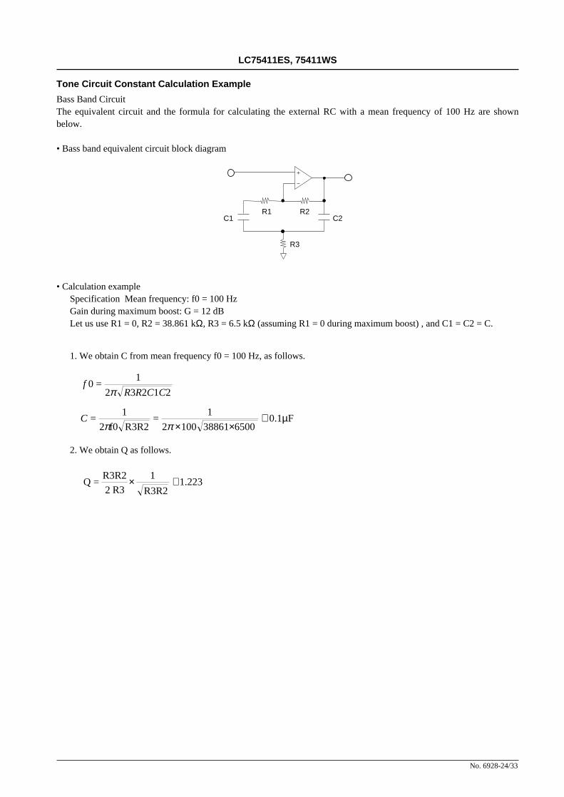
Tone Circuit Constant Calculation Example
Bass Band CircuitThe equivalent circuit and the formula for calculating the external RC with a mean frequency of 100 Hz are shownbelow.
• Bass band equivalent circuit block diagram
1. We obtain C from mean frequency f0 = 100 Hz, as follows.
2. We obtain Q as follows.
No. 6928-24/33
LC75411ES, 75411WS
• Calculation exampleSpecification Mean frequency: f0 = 100 HzGain during maximum boost: G = 12 dBLet us use R1 = 0, R2 = 38.861 kΩ, R3 = 6.5 kΩ (assuming R1 = 0 during maximum boost) , and C1 = C2 = C.
R1 R2
R3
C2C1

Treble Band Circuit
The shelving characteristics for the treble band can be obtained.The equivalent circuit and the calculation formula during boost are shown below.
No. 6928-25/33
LC75411ES, 75411WS
• Calculation exampleSpecification Setting frequency: f = 26000 HzGain during maximum boost: G = 12 dBLet us use R1 = 12.840 kΩ and R2 = 38.861 kΩThe above constants are inserted in the following formula.
R1 R2C
G LOGR2
R C= × +
+20 1
1 110 2 2( / )ω
C
fR2
R1G
=
––
1
210 120
2 2π ( )/
2700(pF)
128401981.3
38861260002
1
22
≅
––
×
=
π

Fader Volume Block Equivalent Circuit Block Diagram
No. 6928-26/33
LC75411ES, 75411WS
LFIN
5.437k
When FADER = "1", S2 and S3 are ON.When FADER = "0", S1 and S4 are ON.
Unit: ΩTotal resistance: 50 kΩ
4.846k
8.169k
4.094k
LFOUT
LVref
–1dB
–2dB
0dB
S1
S2
S3
S4
6.489k
5.154k–6dB
–8dB
–4dB
3.252k
2.583k
2.052k
3.419k
–12dB
–14dB
–10dB
1.630k
1.295k–18dB
–20dB
–16dB
1.300k
0.231k–45dB
–60dB
–∞dB
–30dB
0.050k
LROUT
When –∞ data is sent to the main volume 0.5dBSTEP, S1 and S2 become open, and S3 and S4 simultaneously become ON.

Usage Cautions(1) Data transmission at power ON
• The status of internal analog switches is unstable at power ON. Therefore, perform muting or some othercountermeasure until the data has been set.
• At power ON, initial setting data must be sent once in order to stabilize the bias of each block in a short time.
(2) Description of zero-cross switching circuit operationThe LC75411ES and 75411WS have a function to switch zero-cross comparator signal detection locations, enablingthe selection of the optimum detection location for blocks whose data is to be updated. Basically, the switching noisecan be minimized by inputting the signal immediately following the block whose data is to be updated to the zero-cross comparator, so it is necessary to switch the detection location every time.
LC75411ES, 75411WS Zero-Cross Detection Circuit
No. 6928-27/33
LC75411ES, 75411WS
Volume Tone
Switch
Fader
Zero-crosscomparator
Selector

(3) Zero-cross switching control methodThe zero-cross switching control method consists of setting the zero-cross control bits to the zero-cross detectionmode (D36, D37 = 0), and specifying the detection blocks (D38, D39) before transmitting the data. These control bitsare latched immediately following data transfer, that is to say beforehand in sync with the falling edge of CE, so whenupdating data of volumes, etc., it is possible to perform mode setting and zero-cross switching with one data transfer.An example of control when updating the data of the volume block is shown below.
(4) Zero-cross timer settingIf the input signal becomes lower than the zero-cross comparator detection sensitivity, or if only low-frequencysignals are input, zero-cross detection continues to be impossible, and data is not latched during this time.The zero-cross timer can set a time for forcible latch during such a status when zero-cross detection is not possible.
(5) Cautions related to serial data transfer1. To ensure that the high-frequency digital signals transferred to the CL, DI, and CE pins do not spill over to the
analog signal block, either guard these signal lines with a ground pattern, or perform transmission using shieldedwires.
2. The data format of the LC75411ES and 75411WS uses 8-bit addresses and 44-bit data. When sending data usingmultiples of 8 (when sending 48 bits), use the method described in Figure 1.
Method for Receiving Data Using Multiple of 8 of LC75411ES and 75411WS
Figure 1
For example, to set 25 ms,using T = 0.69CR and C = 0.033 µF,we obtain
Normally, a value between 10 ms and 50 ms is set.
Zero-cross detection mode setting
Volume block setting
No. 6928-28/33
LC75411ES, 75411WS
D36 D37 D38 D39
0 0 1 0
R= 1.1 MΩ25 × 10 –3
0.69 × 0.033 × 10 –6
D43D42D41D40D39D38D37D36D3D2D1D0XXXX
Test mode control Input switching controlDummy data
X : don’t care

No. 6928-29/33
LC75411ES, 75411WS
Gain Step Characteristics Gain Step Characteristics
Out
put l
evel
— d
B
Out
put l
evel
— d
B
Step setting — dB Step setting — dB
LC75411ESVDD=9VVIN=–30dBVInput L1Output LFOUTf=1kHz
LC75411WSVDD=9VVIN=–30dBVInput L1Output LFOUTf=1kHz
Atte
nuat
ion
— d
B
Atte
nuat
ion
— d
B
Step setting — dB Step setting — dB
LC75411ESVDD=9VVIN=0f=1kHzInput L1Output LFOUT
LC75411WSVDD=9VVIN=0f=1kHzInput L1Output LFOUT
Inpu
t gai
n bl
ock
Mai
n vo
lum
e bl
ock
Grap
hic e
quali
zer b
lock
Fad
er b
lock
Inpu
t gai
n bl
ock
Mai
n vo
lum
e bl
ock
Grap
hic e
quali
zer b
lock
Fad
er b
lock
Inpu
t gai
n bl
ock
Mai
n vo
lum
e bl
ock
Grap
hic e
quali
zer b
lock
Fad
er b
lock
Inpu
t gai
n bl
ock
Mai
n vo
lum
e bl
ock
Grap
hic e
quali
zer b
lock
Fad
er b
lock
Main Volume Control Step Characteristics Main Volume Control Step Characteristics

No. 6928-30/33
LC75411ES, 75411WS
Fader Volume Control Step Characteristics Fader Volume Control Step Characteristics
Fade
r V
olum
e A
ttenu
atio
n —
dB
Fade
r V
olum
e A
ttenu
atio
n —
dB
THD — Frequency Characteristics THD — Frequency Characteristics
Tot
al h
arm
onic
dis
tort
ion
— %
Tot
al h
arm
onic
dis
tort
ion
— %
Step setting — dB Step setting — dB
Frequency, f — dB Frequency, f — dB
LC75411ESVDD=9VVIN=0dBVInput L1Output LFOUTf=1kHz
LC75411WSVDD=9VVIN=0dBVInput L1Output LFOUTf=1kHz
LC75411ESVDD=9VInput L1Output LFOUT80kHz LPF
LC75411WSVDD=9VInput L1Output LFOUT80kHz LPF
Inpu
t gai
n bl
ock
Mai
n vo
lum
e bl
ock
Grap
hic e
quali
zer b
lock
Fad
er b
lock
Inpu
t gai
n bl
ock
Mai
n vo
lum
e bl
ock
Grap
hic e
quali
zer b
lock
Fad
er b
lock
Inpu
t gai
n bl
ock
Mai
n vo
lum
e bl
ock
Grap
hic e
quali
zer b
lock
Fad
er b
lock
Inpu
t gai
n bl
ock
Mai
n vo
lum
e bl
ock
Grap
hic e
quali
zer b
lock
Fad
er b
lock
THDMETER
THDMETER

No. 6928-31/33
LC75411ES, 75411WS
THD — Input Level Characteristics THD — Input Level Characteristics
Tot
al h
arm
onic
dis
tort
ion,
TH
D —
%
Tot
al h
arm
onic
dis
tort
ion,
TH
D —
%
Input level, VIN — dBV Input level, VIN — dBV
THD — Supply Voltage Characteristics THD — Supply Voltage Characteristics
Tot
al h
arm
onic
dis
tort
ion,
TH
D —
%
Tot
al h
arm
onic
dis
tort
ion,
TH
D —
%
Supply voltage — VSupply voltage — V
LC75411ESVDD=9V80kHz LPFInput L1, Output LFOUTWith MV=0dB
LC75411ES80kHz LPFInput L1Output LFOUT
LC75411WS80kHz LPFInput L1Output LFOUT
LC75411WSVDD=9V80kHz LPFInput L1, Output LFOUTWith MV=0dB
Inpu
t gai
n bl
ock
Mai
n vo
lum
e bl
ock
Grap
hic e
quali
zer b
lock
Fad
er b
lock
Inpu
t gai
n bl
ock
Mai
n vo
lum
e bl
ock
Grap
hic e
quali
zer b
lock
Fad
er b
lock
THDMETER
Inpu
t gai
n bl
ock
Mai
n vo
lum
e bl
ock
Grap
hic e
quali
zer b
lock
Fad
er b
lock
Inpu
t gai
n bl
ock
Mai
n vo
lum
e bl
ock
Grap
hic e
quali
zer b
lock
Fad
er b
lock
THDMETER
Inpu
t gai
n bl
ock
Mai
n vo
lum
e bl
ock
Grap
hic e
quali
zer b
lock
Fad
er b
lock
Inpu
t gai
n bl
ock
Mai
n vo
lum
e bl
ock
Grap
hic e
quali
zer b
lock
Fad
er b
lock
THDMETER
Inpu
t gai
n bl
ock
Mai
n vo
lum
e bl
ock
Grap
hic e
quali
zer b
lock
Fad
er b
lock
Inpu
t gai
n bl
ock
Mai
n vo
lum
e bl
ock
Grap
hic e
quali
zer b
lock
Fad
er b
lock
THDMETER
No. 6928-32/33
LC75411ES, 75411WS
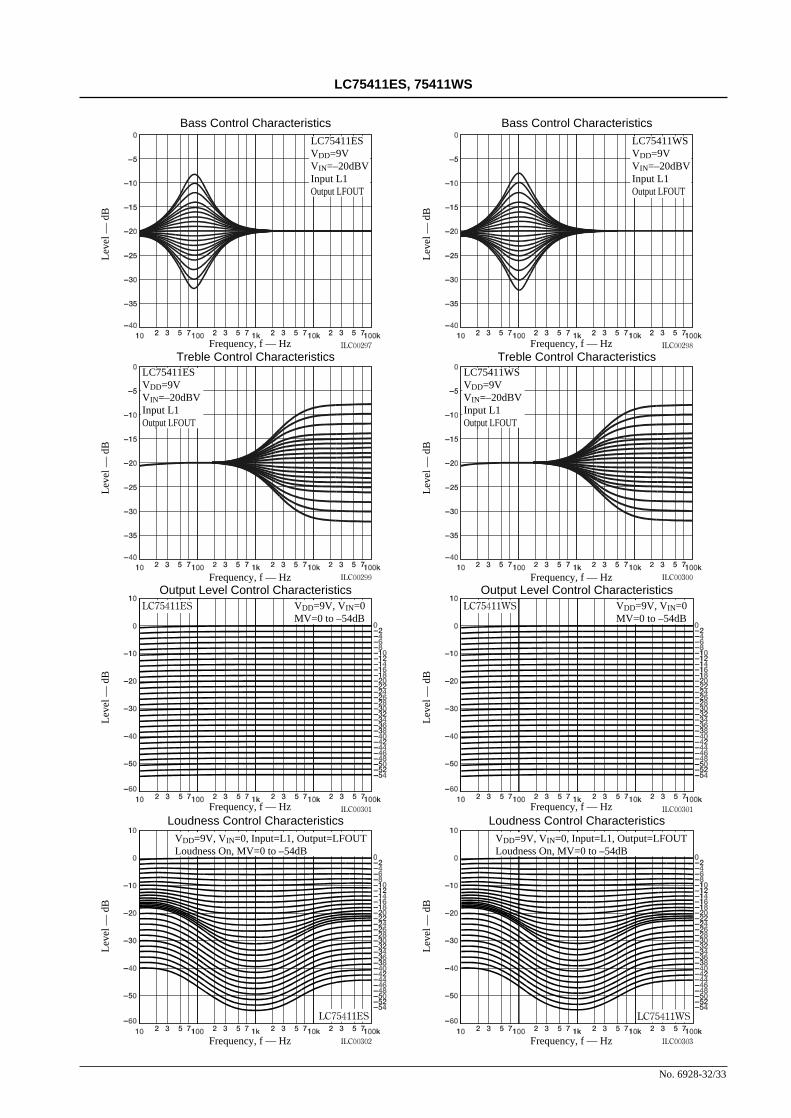
Bass Control Characteristics
Lev
el —
dB
Frequency, f — Hz
LC75411ESVDD=9VVIN=–20dBVInput L1Output LFOUT
LC75411ESVDD=9VVIN=–20dBVInput L1Output LFOUT
VDD=9V, VIN=0MV=0 to –54dB
VDD=9V, VIN=0, Input=L1, Output=LFOUTLoudness On, MV=0 to –54dB
VDD=9V, VIN=0, Input=L1, Output=LFOUTLoudness On, MV=0 to –54dB
VDD=9V, VIN=0MV=0 to –54dB
LC75411WSVDD=9VVIN=–20dBVInput L1Output LFOUT
Bass Control Characteristics
Lev
el —
dB
Frequency, f — HzTreble Control Characteristics
Lev
el —
dB
Frequency, f — Hz
Treble Control Characteristics
Lev
el —
dB
Frequency, f — HzOutput Level Control Characteristics
Lev
el —
dB
Frequency, f — Hz
Output Level Control Characteristics
Loudness Control Characteristics Loudness Control Characteristics
Lev
el —
dB
Lev
el —
dB
Lev
el —
dB
Frequency, f — Hz
Frequency, f — Hz Frequency, f — Hz
LC75411WSVDD=9VVIN=–20dBVInput L1Output LFOUT

PS No. 6928-33/33
LC75411ES, 75411WS
This catalog provides information as of June, 2001. Specifications and information herein are subject tochange without notice.
Specifications of any and all SANYO products described or contained herein stipulate the performance,characteristics, and functions of the described products in the independent state, and are not guaranteesof the performance, characteristics, and functions of the described products as mounted in the customer’sproducts or equipment. To verify symptoms and states that cannot be evaluated in an independent device,the customer should always evaluate and test devices mounted in the customer’s products or equipment.
SANYO Electric Co., Ltd. strives to supply high-quality high-reliability products. However, any and allsemiconductor products fail with some probability. It is possible that these probabilistic failures couldgive rise to accidents or events that could endanger human lives, that could give rise to smoke or fire,or that could cause damage to other property. When designing equipment, adopt safety measures sothat these kinds of accidents or events cannot occur. Such measures include but are not limited to protectivecircuits and error prevention circuits for safe design, redundant design, and structural design.
In the event that any or all SANYO products (including technical data, services) described or containedherein are controlled under any of applicable local export control laws and regulations, such products mustnot be exported without obtaining the export license from the authorities concerned in accordance with theabove law.
No part of this publication may be reproduced or transmitted in any form or by any means, electronic ormechanical, including photocopying and recording, or any information storage or retrieval system,or otherwise, without the prior written permission of SANYO Electric Co., Ltd.
Any and all information described or contained herein are subject to change without notice due toproduct/technology improvement, etc. When designing equipment, refer to the “Delivery Specification”for the SANYO product that you intend to use.
Information (including circuit diagrams and circuit parameters) herein is for example only; it is notguaranteed for volume production. SANYO believes information herein is accurate and reliable, butno guarantees are made or implied regarding its use or any infringements of intellectual property rightsor other rights of third parties.

This datasheet has been download from:
www.datasheetcatalog.com
Datasheets for electronics components.