Embed Size (px)
Citation preview

MAINTENANCE MANUALFOR 806-869 MHz
PERSONAL TWO-WAY FM RADIO COMBINATION
INTRODUCTION
The recommended troubleshooting procedure, as illus-trated in Figure 1, is to isolate the fault to a specific sectionof the M-RK Personal radio ; the radio section ; the logicsection or the battery pack. Then further localize the fault toa specific stage of the suspected section. The last step is toisolate and identify the defective component.
LBI-38749B
TABLE OF CONTENTS
Page
INTRODUCTION . . . . . . . . . . . . . . . . . . . . . . . . . . . . . . . . . . . . . . . . . . . . . . . . . . . 1
PHASE 1 : RADIO SECTION TROUBLESHOOTING
Functional Troubleshooting Flow Chart . . . . . . . . . . . . . . . . . . . . . . . . . . . . . . . . . . . . . 3
SynthesizerFlow Chart . . . . . . . . . . . . . . . . . . . . . . . . . . . . . . . . . . . . . . . . . . . . . . . . . 4Troubleshooting for Synthesizer . . . . . . . . . . . . . . . . . . . . . . . . . . . . . . . . . . . . . . 4
ReceiveFlow Chart . . . . . . . . . . . . . . . . . . . . . . . . . . . . . . . . . . . . . . . . . . . . . . . . . 8Troubleshooting for Receiver . . . . . . . . . . . . . . . . . . . . . . . . . . . . . . . . . . . . . . . . 8
TransmitFlow Chart . . . . . . . . . . . . . . . . . . . . . . . . . . . . . . . . . . . . . . . . . . . . . . . . . 11Troubleshooting for Transmitter . . . . . . . . . . . . . . . . . . . . . . . . . . . . . . . . . . . . . . 11
PHASE 2 : LOGIC SECTION TROUBLESHOOTING
Major Troubleshooting flow chart . . . . . . . . . . . . . . . . . . . . . . . . . . . . . . . . . . . . . . . . 13
Functional Troubleshooting
Flow chart . . . . . . . . . . . . . . . . . . . . . . . . . . . . . . . . . . . . . . . . . . . . . . . . . . . . 13
Troubleshooting for Logic Section . . . . . . . . . . . . . . . . . . . . . . . . . . . . . . . . . . . . . . . 14
LOGIC SECTION CHECK LIST . . . . . . . . . . . . . . . . . . . . . . . . . . . . . . . . . . . . . . . . . . . 16
TRACKING DATA . . . . . . . . . . . . . . . . . . . . . . . . . . . . . . . . . . . . . . . . . . . . . . . . . . 21
MAINTAINING WEATHER PROOF INTEGRITY . . . . . . . . . . . . . . . . . . . . . . . . . . . . . . . . . 21
MODULE AND INTEGRATED CIRCUIT DATA . . . . . . . . . . . . . . . . . . . . . . . . . . . . . . . . . . 22
Figure 1 - Recommended Troubleshooting Procedure
ericssonz

The following list of test equipment is recommendedwhen servicing or troubleshooting the M-RK Personal Ra-dio.
Recommended Test Equipment :
• Audio Analyzer
• Digital Voltmeter
• DC Power Supply
• Multimeter
• Oscilloscope
SERVICING SETUP
The servicing setup is shown in Figure 1A. This illus-trates the test boxes, cables, etc. required when the M-RKneeds to be disassembled for troubleshooting or servicing.
MAINTENANCE/WARRANTY
1. Repair and Return is available at Authorized Serv-ice Centers (ASC) or at Ericsson Inc., inLynchburg, VA.
Copyright © December 1992, Ericsson GE Mobile Communications Inc.
Figure 1A - Servicing Setup
LBI-38749
2

2. Board level Repair and Return is recommended.Servicing to component level is not recommended.
3. Parts and components available through ServiceParts are shown and listed in LBI-38746. When or-dering replacement parts, please add the prefix"K19/" to the listed part number.
4. Standard warranty (3 months labor, 12 monthsparts) applies. Option PKCSIP extends labor war-ranty to 12 months.
PHASE 1 : RADIO SECTIONTROUBLESHOOTING
FUNCTIONAL TROUBLESHOOTING
Once the fault has been isolated to the radio section, thenext step is to further isolate the fault to a specific stage ofthe radio section; Frequency Synthesizer (SYN), Receive(RX) and Transmit (TX). The flowchart (See Page 2) willassist in isolating the fault to a specific stage of the radiosection.
Functional Troubleshooting Flowchart:
LBI-38749
3

SYNTHESIZER
The following flowchart can be used to isolate a defec-tive stage in the synthesizer circuit.
Synthesizer Flowchart :
Troubleshooting for the Synthesizer :
1. 6.0 Volt Regulator
The 6.0 volt regulator consists of regulator U6 andtransistor Q105. If a fault is found with the regu-lated 6.0 volt output line, trace the fault sourcealong this line back to the regulator. A typical cur-rent flowing is 30 mA. Typical voltages for thesynthesizer are shown in Table 1.
Any repair should be made so that the current andvoltage at each assembly and component agreeswith the typical value.
2. Reference Oscillator VCTCXO (Z1)
The reference oscillator is contained in one assem-bly. Typical data, when the reference oscillator isworking properly, is shown in Table 2.
Table 2 - Typical Data For The Reference Oscillator
Item Typical Value Remarks
Supply Voltage 5.3 Vdc
Current DrainOutput Frequency
1.5 to 1.8 mA13.2 MHz
Output Level 1 to 2 Vp-p
3. Prescaler Output Level
VCO U5 has an output level of about 0 dBm. Partof the VCO output is applied to the input of bufferamplifier transistor Q101 through a capacitor. Af-ter amplification, the output is applied to the inputof the Prescaler, which is operating under 128/129modulus control. A typical prescaler output level is1 volt p-p, which is applied to the input of thePLL.
When checking the prescaler, refer to the typicalvalue on Table 1.
4. Phase-Lock-Loop (U2)
a. Check for approximately 1 to 2 volts p-p ref-erence signal input at Pin 2 of U2.
b. Check that the reference signal frequency is13.2 MHz and that frequency stability is ±1.5PPM.
LBI-38749
4

c. Measure the input from the prescaler at Pin 10of U2 and verify approximately 1 volt p-p in-put level.
d. Verify that approximately 5 volts p-p (Vss-Vcc) control pulse is present at Pin 8 of pres-caler control U2.
e. Cause the PLL to unlock. Then check for thepresence of approximately 5 volts p-p (Vss-Vcc) PD and FD pulse outputs at Pin 6 andPin 17 of U2 respectively. Also check for ap-proximately 6 volts p-p (Vss+B) at Pin 1 ofU4. If the pulse output is absent or shifted toeither the Vss or the Vcc side, the PLL mayfail to lock over a certain section of the fre-quency range or the entire range. If this faultoccurs, the possible trouble source is ramp re-sistor R111, ramp capacitor C131 or hold ca-pacitor C132.
f. Verify that the local voltages at the test pointslisted on Table 1 agree with the typical valuesalso listed on Table 1.
g. Verify that the CLOCK, DATA, ENABLE andWIDE/NARROW signals coming from theControl Board are at the proper level and theproper duration (refer to Figure 2).
If the CLOCK and DATA are improper, thePLL operation will become erratic. If the du-ration of the W/N pulse is shorter than 10 mil-liseconds, which is the minimum value, thePLL may fail to lock.
Table 1 - Synthesizer Portion Typical Voltages
No. Test Points Voltage (V) Remarks
1 U1 (1) 3.0
2 U1 (2) 5.3
3 U1 (3) 0 (GND)
4 U1 (4) 1.2p-p VL : 3.2, VH : 4.4
5 U1 (5) 0 (GND)
6 U1 (6) 4.8p-p VL : 0.6, VH : 5.4
7 U1 (7) —
8 U1 (8) 3.0
9 U2 (1) 4.4
10 U2 (2) 1.6p-p VL : 1.6, VH : 3.2
11 U2 (5) (19) 5.6
12 U2 (6) (17) 1.4(RX), 1.2(Tx) at 806 MHz
13 U2 (8) 4.8p-p VL : 0.6, VH : 5.4
14 U2 (9) 5.5
15 U2 (10) 1.2p-p VL : 1.8, VH : 3.0
16 U2 (11) 0
17 U2 (12) 0
18 U2 (13) 0
19 U2 (15) 2.1o-p(Rx),1.9o-p(Tx
at 806 MHz
20 U2 (18) 0.2p-p VL:2.4,VH:2.6(Rx),VL:2.1,VH:2.3(Tx),
21 U2 (20) 3.9
22 Z1 (3) 4.9
23 U4 (1) 1.9(Rx), 1.6 (Tx) at 806 MHz
24 U4 (2) 1.5(Rx), 1.2 (Tx)
25 U4 (3) 1.4(Rx), 1.2 (Tx) at 806 MHz
26 U4 (4) (5) 0 (GND)
27 U4 (6) 0 (GND)
28 U4 (7) —
29 U4 (8) 7.4
If parts other than those specified in theparts list are used in the associated circuitof the PLL, the switching time may be af-fected. Whenever any parts are replaced Inthe associated circuit, check the switchingtime.
NOTE
LBI-38749
5

No. Test Points Voltage (V) Remarks
30 U3 (9) (10) 1.9(Rx), 1.6(Tx) at 806 MHz (Hiimpedance)
31 U3 (9) (10) 1.9(Rx), 1.6(Tx) at 806 MHz
32 U3 (6) (12) 0
33 U3 (5) (13) 0 (GND)
34 U3 (7) 0 (GND)
35 U3 (2) (3) 0 (GND)
36 U3 (1) (4) 0 (GND)
37 U3 (14) 6.0
38 U5 (1) 0.1 (Rx), 3.9(Tx)
39 U5 (3) 0
40 U5 (4) 5.2
41 U5 (5) 0
42 U5 (7) 5.0(Rx), 1.6(Tx)
43 U5 (10) 5.1
44 U5 (12) 1.9(Rx), 1.6(Tx) at 806 MHz (Hiimpedance)
45 U5 (2) (6) (8)(9) (11) (13)(14)
0 (GND)
46 Q101 Base 1.4
47 Q101 Emitter 0.3
48 Q101Collector
6.0
49 Q102 (1) 5.0 (Rx), 0.2(Tx)
50 Q102 (2) (3) 0.1(Rx), 3.9(Tx)
51 Q102 (4) 5.0 (Rx), 0(Tx)
52 Q103 (5) (6) 0 (GND)
53 Q103 Base 1.2
54 Q103 Emitter 0.6
55 Q103Collector
6.7
56 Q105 (1) 0 (GND)
57 Q105 (2) 7.5
58 Q105 (3) 0
No. Test Points Voltage (V) Remarks
59 Q106 Base 5.8
60 Q106 Emitter 5.2
61 Q106Collector
6.0
62 Q107 Base 7.4
63 Q107 Emitter 6.8
64 Q107Collector
7.5
5. VCO Control Voltage
a. VCO Control Voltage should be :
• Approximately 1 volt or more at the lowestchannel of any band.
• Approximately 4.5 volts or less at the highestchannel of any band.
Verify the VCO control voltage at the testpointTPPD using a high-impedance oscilloscope.
6. Switching Time
The channel frequency must be locked within 10milliseconds, which is the duration of the Wide/Narrow pulse. That is, the switching time is re-stricted by the Wide/Narrow pulse.
a. Switching time is largely influenced by theleakage current characteristics of C133 andC152. Be sure to use parts having the ratingsspecified on the Parts List when replacingthese parts. Also, if moisture collects on theprinted wire board, the Insulation resistance ofthe board may be lowered, also affecting theswitching time.
Figure 2 - Clock, Data, Enable, and Wide/NarrowSignals
LBI-38749
6
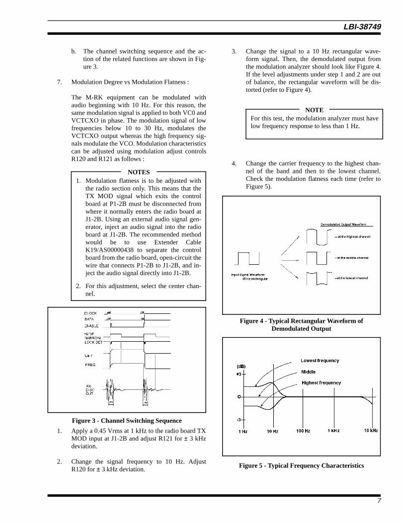
b. The channel switching sequence and the ac-tion of the related functions are shown in Fig-ure 3.
7. Modulation Degree vs Modulation Flatness :
The M-RK equipment can be modulated withaudio beginning with 10 Hz. For this reason, thesame modulation signal is applied to both VC0 andVCTCXO in phase. The modulation signal of lowfrequencies below 10 to 30 Hz, modulates theVCTCXO output whereas the high frequency sig-nals modulate the VCO. Modulation characteristicscan be adjusted using modulation adjust controlsR120 and R121 as follows :
1. Apply a 0.45 Vrms at 1 kHz to the radio board TXMOD input at J1-2B and adjust R121 for ± 3 kHzdeviation.
2. Change the signal frequency to 10 Hz. AdjustR120 for ± 3 kHz deviation.
3. Change the signal to a 10 Hz rectangular wave-form signal. Then, the demodulated output fromthe modulation analyzer should look like Figure 4.If the level adjustments under step 1 and 2 are outof balance, the rectangular waveform will be dis-torted (refer to Figure 4).
4. Change the carrier frequency to the highest chan-nel of the band and then to the lowest channel.Check the modulation flatness each time (refer toFigure 5).
1. Modulation flatness is to be adjusted withthe radio section only. This means that theTX MOD signal which exits the controlboard at P1-2B must be disconnected fromwhere it normally enters the radio board atJ1-2B. Using an external audio signal gen-erator, inject an audio signal into the radioboard at J1-2B. The recommended methodwould be to use Extender CableK19/AS00000438 to separate the controlboard from the radio board, open-circuit thewire that connects P1-2B to J1-2B, and in-ject the audio signal directly into J1-2B.
2. For this adjustment, select the center chan-nel.
NOTES
For this test, the modulation analyzer must havelow frequency response to less than 1 Hz.
NOTE
Figure 3 - Channel Switching Sequence
Figure 4 - Typical Rectangular Waveform ofDemodulated Output
Figure 5 - Typical Frequency Characteristics
LBI-38749
7
If a large level difference is found between the modula-tion characteristics at 10 Hz and those at 100 Hz when thecarrier frequency is changed from the highest to the lowest,the problem Is with the VCO modulation characteristics.
When the waveform of the demodulated output Is dis-torted for a modulation frequency of 10 Hz or lower, theproblem is with the VCTCXO. If the distortion is substan-tial, the carrier frequency may be affected by modulation.
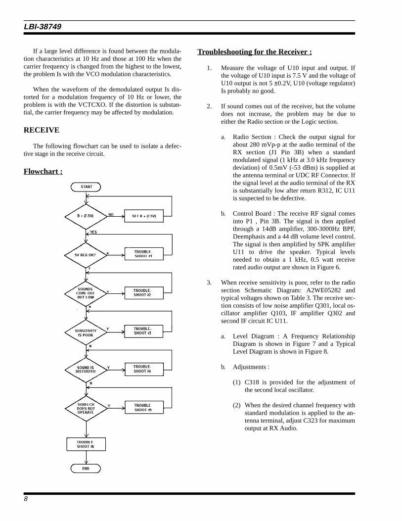
RECEIVE
The following flowchart can be used to isolate a defec-tive stage in the receive circuit.
Flowchart :
Troubleshooting for the Receiver :
1. Measure the voltage of U10 input and output. Ifthe voltage of U10 input is 7.5 V and the voltage ofU10 output is not 5 ±0.2V, U10 (voltage regulator)Is probably no good.
2. If sound comes out of the receiver, but the volumedoes not increase, the problem may be due toeither the Radio section or the Logic section.
a. Radio Section : Check the output signal forabout 280 mVp-p at the audio terminal of theRX section (J1 Pin 3B) when a standardmodulated signal (1 kHz at 3.0 kHz frequencydeviation) of 0.5mV (-53 dBm) is supplied atthe antenna terminal or UDC RF Connector. Ifthe signal level at the audio terminal of the RXis substantially low after return R312, IC U11is suspected to be defective.
b. Control Board : The receive RF signal comesinto P1 , Pin 3B. The signal is then appliedthrough a 14dB amplifier, 300-3000Hz BPF,Deemphasis and a 44 dB volume level control.The signal is then amplified by SPK amplifierU11 to drive the speaker. Typical levelsneeded to obtain a 1 kHz, 0.5 watt receiverated audio output are shown in Figure 6.
3. When receive sensitivity is poor, refer to the radiosection Schematic Diagram: A2WE05282 andtypical voltages shown on Table 3. The receive sec-tion consists of low noise amplifier Q301, local os-cillator amplifier Q103, IF amplifier Q302 andsecond IF circuit IC U11.
a. Level Diagram : A Frequency RelationshipDiagram is shown in Figure 7 and a TypicalLevel Diagram is shown in Figure 8.
b. Adjustments :
(1) C318 is provided for the adjustment ofthe second local oscillator.
(2) When the desired channel frequency withstandard modulation is applied to the an-tenna terminal, adjust C323 for maximumoutput at RX Audio.
LBI-38749
8
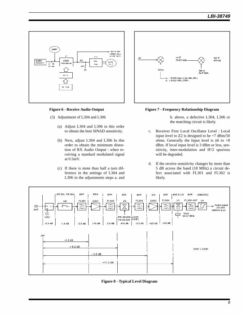
(3) Adjustment of L304 and L306
(a) Adjust L304 and L306 in this orderto obtain the best SINAD sensitivity.
(b) Next, adjust L304 and L306 In thisorder to obtain the minimum distor-tion of RX Audio Output : when re-ceiving a standard modulated signalat 0.5mV.
(c) If there is mote than half a turn dif-ference in the settings of L304 andL306 in the adjustments steps a. and
b. above, a defective L304, L306 orthe matching circuit is likely.
c. Receiver First Local Oscillator Level : Localinput level to Z2 is designed to be +7 dBm/50ohms. Generally the Input level is ±6 to +8dBm. If local input level is 3 dBm or less, sen-sitivity, inter-modulation and IF/2 spuriouswill be degraded.
d. If the receive sensitivity changes by more than5 dB across the band (18 MHz) a circuit de-fect associated with FL301 and FL302 islikely.
Figure 6 - Receive Audio Output Figure 7 - Frequency Relationship Diagram
Figure 8 - Typical Level Diagram
LBI-38749
9

Table 3 - Receive Section Typical Voltages
No. Test Points Voltage (V) Remarks
1 Q301 1.5
2 Q301 0.8
3 Q301 5.8
4 Q302 1.2
5 Q302 0.4
6 Q302 4.0
7 U10 (1) 0 (GND)
8 U10 (2) 7.4
9 U10 (3) 5.0
10 U11 (1) (13)(20)
0 (GND)
11 U11 (2) 3.0
12 U11 (3) 3.0
13 U11 (4) 3.0
14 U11 (5) 2.4
15 U11 (6) 3.3
16 U11 (7) 3.2
17 U11 (8) 3.2
18 U11 (9) 2.6
19 U11 (10) 3.3
20 U11 (11) 0.9
21 U11 (12) 0.6
22 U11 (14) 0.7
23 U11 (15) 0.7
24 U11 (16) —
25 U11 (17) —
26 U11 (18) —
27 U11 (19) 4.1
28 U11 (21) 1.1
29 U11 (22) 4.1
30 U11 (23) 3.4
No. Test Points Voltage (V) Remarks
31 U11 (24) 3.9
32 U12 (1) 0.9
33 U12 (2) 0.9
34 U12 (3) 0 (GND)
35 U12 (4) 5.0
36 U12 (5) 5.0
4. If distortion in the received signal is substantiallyhigh, try to perform checks with the Radio andControl Board Individually.
a. Check the Local Oscillator Frequency. Checkthe frequency after connecting a frequencycounter through a 1 PF capacitor to the collec-tor of Q103. The frequency relation at variousstages is shown In Figure 8. If a frequency er-ror is 1.5 PPM or more in the temperaturerange of 20 to 25C, adjust the frequency ofVCTCXO (Z1). The frequency of VCTCXOis 13.2 MHz.
b. Check the Usable Band Width. Usable bandwidth is generally ±2.5 kHz or more of the de-sired receiving frequency. If the ±balance isgreatly different, the received signal may bedistorted. This time, the problem is probablycaused by FL303, FL304, FL305, FL306,FL307 or its associated components.
c. Distortion Check : When the radio receives astandard modulated signal, the audio output atthe Audio terminal J1-3B (P1-3B) is about280mVp-p. At this point, the distortion will beabout 3%. This is because the receiver dis-criminator output is connected to the RXAudio terminal and de-emphasis and BP Fil-tering has not, at this point, been provided.Because considerable noise is contained fromlow audio frequencies to high audio frequen-cies, use test equipment with a high input im-pedance (100K ohms) for the distortionmeasurement.
d. The signal from the Radio Board is applied tothe Control Board at P1-3B and then to thespeaker through U7 and U11. Check distortionat each point.
LBI-38749
10
e. Even if there are no electrical problems withthe audio circuits on the Control Board, thespeaker itself may cause distortion mechani-cally. The voice coil may rub or the diaphrammay be damaged or touching another part ofthe radio.
5. Noise Squelch does not operate :
A part of receiver discriminator output is appliedto the Control Board through J1-3B (P1-3B).
a The operation of squelch is controlled byAudio Processor U7 on the Control Board.
b. The squelch operation level is set in the chan-nel data E2PROM. Refer to E2PROM Pro-gramming.
6. Other Problems and Cautions :
a. A polyimide flex circuit is used at theLCD/KB Flex Assy. If the LCD/KB Flex Assyis repeatedly disassembled for maintenance,the flex circuit can be damaged. Accordingly,keep disassembly of the Control Unit at aminimum.
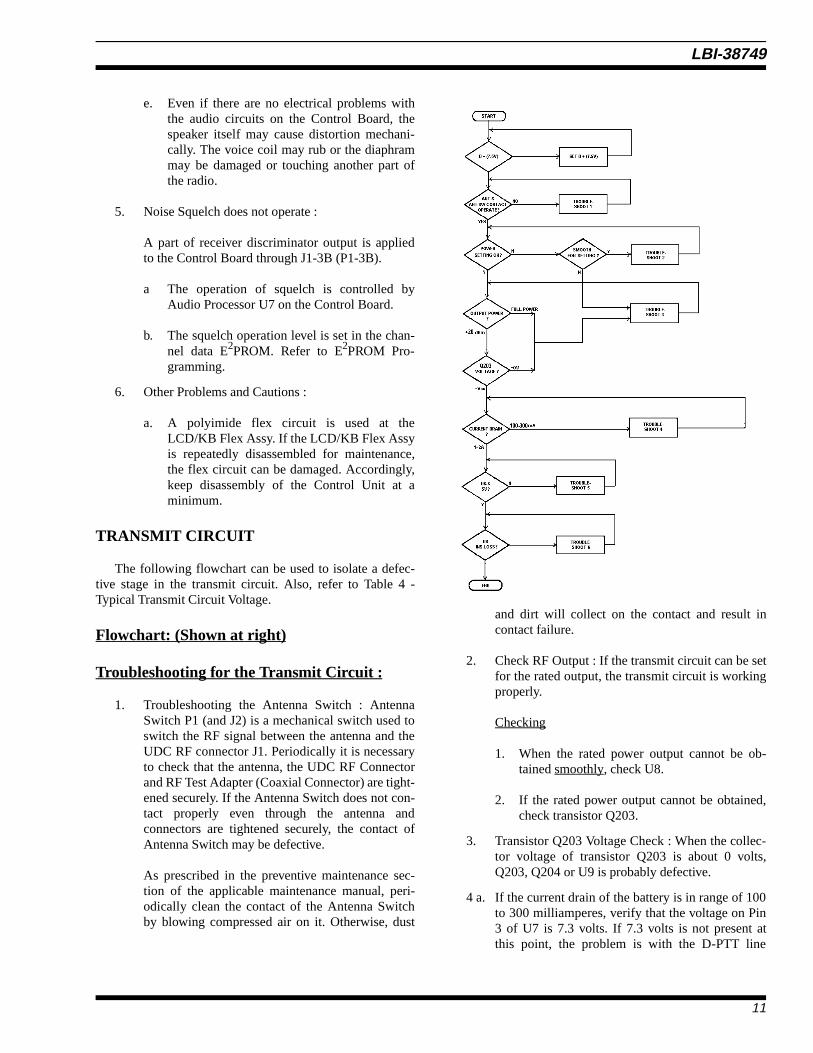
TRANSMIT CIRCUIT
The following flowchart can be used to isolate a defec-tive stage in the transmit circuit. Also, refer to Table 4 -Typical Transmit Circuit Voltage.
Flowchart: (Shown at right)
Troubleshooting for the Transmit Circuit :
1. Troubleshooting the Antenna Switch : AntennaSwitch P1 (and J2) is a mechanical switch used toswitch the RF signal between the antenna and theUDC RF connector J1. Periodically it is necessaryto check that the antenna, the UDC RF Connectorand RF Test Adapter (Coaxial Connector) are tight-ened securely. If the Antenna Switch does not con-tact properly even through the antenna andconnectors are tightened securely, the contact ofAntenna Switch may be defective.
As prescribed in the preventive maintenance sec-tion of the applicable maintenance manual, peri-odically clean the contact of the Antenna Switchby blowing compressed air on it. Otherwise, dust
and dirt will collect on the contact and result incontact failure.
2. Check RF Output : If the transmit circuit can be setfor the rated output, the transmit circuit is workingproperly.
Checking
1. When the rated power output cannot be ob-tained smoothly, check U8.
2. If the rated power output cannot be obtained,check transistor Q203.
3. Transistor Q203 Voltage Check : When the collec-tor voltage of transistor Q203 is about 0 volts,Q203, Q204 or U9 is probably defective.
4 a. If the current drain of the battery is in range of 100to 300 milliamperes, verify that the voltage on Pin3 of U7 is 7.3 volts. If 7.3 volts is not present atthis point, the problem is with the D-PTT line
LBI-38749
11

(Q201, Q202). Check to see if there is an open- ora short- circuit on other lines on the Vcc line.
b. If 7.3 volts is present at the above pins, check thatvoltage at collector of Q104 . If so, then check theoutput level of U5 (VCOT0).
c. When the output of U5 is around 0 dBm, the prob-lem is Q104. When the output level is -5 dBm orlower, the VCO in the synthesizer circuit is prob-ably defective. Try the troubleshooting procedurefor the Synthesizer to verify the trouble with theVCO.
5. Checking Voltage at U8 : Under normal conditions,the voltage at the Pin 6 of U8 is 5 volts. If 5 voltsis not present at this point, refer to troubleshoot 4.
6. Checking the U8 (LPF.DC.T/R SW) Insertion Loss: If an increase in the insertion loss of the U8 issuspected, the problem is U8.
Table 4 - Typical Transmit Voltages
No. Test Points Voltage (V) Remarks
1 U7 (1) —
2 U7 (2) 0 (Rx), 3.7 (Tx) Changed by power level
3 U7 (3) 0 (Rx), 7.3 (Tx)
4 U7 (4) 7.4
5 U7 (5) —
6 U7 (6) 0 (GND)
7 U8 (2) —
8 U8 (4) 0 (Rx), 2.5 (Tx) Changed by power level
9 U8 (6) 0 (Rx), 5.0 (Tx)
10 U8 (8) 0 (Rx), 1.6 (Tx)
11 U8 (13) —
12 U8 (1) (3) (5)(7) (9) (11)(12) (14)
0 (GND)
13 Q104 Base 0 (Rx), 1.4 (Tx)
No. Test Points Voltage (V) Remarks
14 Q104 Emitter 0 (Rx), 0.8 (Tx)
15 Q104Collector
0 (Rx), 7.2 (Tx)
16 Q201 (1) 7.5 (Rx), 0 (Tx)
17 Q201 (2) 0 (Rx), 5.0 (Tx)
18 Q201 (3) 5.0 (Rx), 0 (Tx)
19 Q201 (4) 0 (Rx), 5.0 (Tx)
20 Q201 (5) 0 (GND)
21 Q201 (6) 0 (GND)
22 Q202 (1) 7.5 (Rx), 0 (Tx)
23 Q202 (2) 0 (Rx), 7.3 (Tx)
24 Q202 (3) 7.4
26 Q203 Base 7.5 (Rx), 6.8 (Tx)
27 Q203 Emitter 7.4
28 Q203Collector
0 (Rx), 3.7 (Tx) Changed by power level
29 Q204 Base 0 (Rx), 1.7 (Tx) Changed by power level
30 Q204 Emitter 0 (Rx), 1.1 (Tx) Changed by power level
31 Q204Collector
7.5 (Rx), 6.8 (Tx) Changed by power level
32 Q205 (1) 5.0
33 Q205 (2) 5.0 (Rx), 0 (Tx)
34 Q205 (3) 0 (Rx), 5.0 (Tx)
35 U9 (5) 3.6 (Rx), 2.4 (Tx) Changed by power level
36 U9 (6) 0 (Rx), 2.4 (Tx) Changed by power level
37 U9 (7) 0 (Rx), 1.7 (Tx) Changed by power level
38 U9 (8) 0 (Rx), 4.9 (Tx)
39 U9 (2) (3) (4) 0 (GND)
LBI-38749
12

PHASE 2 : LOGIC SECTIONTROUBLESHOOTING
MAJOR TROUBLESHOOTING : (DISPLAYAND SWITCH ACTION)
The flowchart (Display and Switch Action)can be usedto isolate any defective stage located on the Control and theLCD/KB Flex Assy.
Flowchart (Internal Display and SwitchAction)
LBI-38749
13

Functional Troubleshooting : (External Inputand Output Action)
The flowchart (External Input and Output Action) canbe used to externally function test the Control Boardthrough the UDC.
LCD/KB Flex Assy : The flowchart (LCD/KB FlexAssy) can be used to isolate any defective stage located onthe LCD/KB Flex Assy.
Flowchart (LCD/KB Flex Assy)
Troubleshooting for Logic Section
1. This troubleshooting should be made with theControl Board isolated from the Radio Board.
2. If the result is OK at Step 1, the E2PROM data(Channel No.) is displayed when power is ON. Inthe unlocked state of the Phase-Lock-Loop (PLL)UN-LOCK display is turned on and off at PTT.
3. If the result is OK at Step 2, the display shouldflicker in the unlocked state.
4. Step 3 indicated that the various switches are actu-ated in the sequence determined with the E2PROMdata.
5. At Step 4, with 1 kHz, -20 dBV signal applied toRX, DISC terminal, check for 0.5 watt/16 ohmoutput to be present at the AUDIO OUT terminal.
It should also be noted that when the initial VOLATT setting is not at 0.5 watt/16 ohm, operate theAF, VOL (R8) for a volume level of 0.5 watt.
6. At Step 5, when the PTT line is grounded, the ra-dio set is switched to the TRANSMIT mode. Thenthe PTT button on the side of the radio should bereleased.
When the transmit mode is verified, apply 1 kHz, -40 dBV signal to the EXT MIC terminal from theAudio Analyzer. Check that a -7dBV +2 dB signalappears at the TX AUDIO terminal (Pin 2B of P1).Take note that the output at TX AUDIO is not sub-jected to limiting and without Channel Guard.
7. At Step 6, generate an arbitrary radio data with adata loader and try to load the data in the E2PROMCheck that data is loaded properly.
8. To perform an internal microphone (INT MIC)test, press and hold the PTT button and speak intothe internal microphone. Check that an audio sig-nal appears at Pin 2B of P1 (TX AUDIO terminal).
LBI-38749
14

Flowchart : (External Input and Output Action)
LBI-38749
15

Logic Section Check List :
MEASURING INSTRUMENT
Digital VoltmeterDC Power SupplyFrequency Counter
ITEM TEST PROCEDURE
1. Preliminary1-1 Voltage Check
There are two regulated supply lines. Conduct voltage check at each check pointas under.
Check Point Rated VoltageU9 - Pin 1 5.0 V ±0.2 V for ControlU10 - Pin 3 5.0 V ±0.2 V for Audio
1-2 Battery Out Check Check that the voltage of Battery or DC Power Supply is present at P1-1B,P2-14B and P2-15b.
1-3 Oscillator Frequency Check Check Crystal "Y1" (IC U2-Pin 69) with frequency counter. The frequencyshould be within 9.8304 MHz ±300 Hz. Check Crystal
LBI-38749
16

MEASURING INSTRUMENT
Audio AnalyzerOscilloscopeDigital VoltmeterDC Power SupplyMultimeter
ITEM TEST PROCEDURE
2. Preliminary2-1 LCD/KB FLEX
1. Check LCD/KB FLEX by turning power supply on.
Insert connector (J1) on LCD/KB FLEX into P2 on Control Board. Then turn power on and check that the data from Control Board is displayed in the LCB/KB FLEX.
3. SW Check and UDC Check 2-a. Operation for each switch, check whether each SW is operated or not by multimeter. Check List
SW-Name Connector Pin No. to be checked
AF. VOLPTTMONOPTEMR
4B1A
J1 11A/13B12A/13B12B/13B
LCD/KB Flex Assy.
LBI-38749
17

ITEM TEST PROCEDURE
2-b UDC Check.
Check List
4. RX S/N Measurement Set Audio Analyzer for 1 kHz, -20 dBv output. Apply this 1 kHzsignal to RX AUDIO IN P1 Pin 3B. Turn AF. VOL> to getMaximum output and check that the level at RX AUDIO OUT of P3PIN 8B (-10 dBv or more) on Oscilloscope.
Adjust CAL control on AUDIO Analyzer for "0". Turn 1 kHz signaloff. Check that noise level is -45 dB or less.
5. RX Frequency Response Set Audio Analyzer for 1 kHz, -30 dBv output. Apply this 1 kHzsignal to RX AUDIO IN P1 PIN 3B. Check that the level at RXAUDIO OUT of P3 PIN 3B is -20 dBv on Levelmeter andOscilloscope. Adjust CAL control on Audio Analyzer for "0" to turn1 kHz signal off. Change the OSC frequency from 210 Hz, 270 Hz,300 Hz and 310 Hz to 10 kHz. Plot AUDIO OUT level on a graph.Check that the level from 300 Hz to 3 kHz is in the range of +1 dBto -3 dB from octave.
LBI-38749
18

ITEM TEST PROCEDURE
6. RX Audio Distortion Measurement Set Audio Analyzer for 1 kHz. Apply this 1 kHz signal to RX AUDIO IN P1PIN 3B. Adjust until Levelmeter and Oscilloscope show that the P3 PIN 8B Is-10 dBV.
Check that Audio Analyzer distortion meter shows 5% or less at this time.
Alternatively it is permitted to use SPEAKER AUDIO OUT as the check point.
7. CG Opening Level Measurement Set Audio Analyzer for 67 Hz to 210.7 Hz. Apply this 67 Hz signal to RXAUDIO IN P1 PIN 3B. Decrease the level of Audio Analyzer until the squelchopens. Check that the opening level is about -38dBV.
NOTE : Use the channel with CG tone in this test.
8. SQ Operation Set Audio Analyzer for 10 kHz. Apply this 10 kHz signal to RX AUDIO IN P1PIN 3B.
Check the output voltage for U2 Pin 59 on Control Board and plot the level ona graph. It is permitted that only the opening level and the closing level ofsquelch are checked.
9. TX S/N Measurement On Test Set, set PTT switch to PTT and check that the Unit goes into transmitmode. Set Audio Analyzer to 1 kHz -40dBV. Apply this 1 kHz signal to EXTMIC Terminal of Test Set. There should be about -7 dBV signal at TX AUDIOOUT at P1 PIN 2B. Adjust CAL control on Analyzer to null. Then turn theAnalyzer output off. The S/N ratio should be 40 dB or better.
10. TX Distortion Measurement Under the same test condition as with S/N measurement, measure distortionwith the Audio Analyzer. The distortion should be less than 3%.
11. TX Frequency Response Set Audio Analyzer for 1 kHz, -50 dBV. Apply this 1 kHz signal to EXT MICTerminal of Test Set. Check that -17dBV signal is present at TX AUDIO OUTat P1 2B. Adjust CAL control on Audio Analyzer for null indication. Turn offthe 1 kHz signal from Analyzer. Then change the output frequency of OSC 210kHz, 260 Hz, 300 Hz to 2.9 kHz and 2.9 kHz to 10 kHz. Plot the changes inthe output signal level on a graph. Check that the frequency response curve iswithin +1, -3 dB over a 300 to 3000 Hz range.
12. Measurement of CG Encode Set PTT Switch to OFF on Test Set. Select that Level and Distortion channelfor which SIG appears on the LCD. Change PTT Switch to PTT side. Checkthat either 67 Hz to 210.7 Hz CG waveform is present at TX AUDIO OUTusing an oscilloscope. Measure the CG signal level (-19 dBV is referencelevel). Check that the distortion in the CG waveform is less than 5%.
13. Power Set Action With the PTT Switch in the PTT Position, check with digital voltmeter that 2.0to 4.0 V is present at PIN 2A of P1.
14. Syn. Clock, Syn. Data, Syn. Enableand Syn. Wide/Narrow Output
Using an Oscilloscope, check that Enable signal is present at PIN 7B of P1,Data at PIN 8A, Clock at PIN 8B and Wide/Narrow at PIN 6A. In this testLOCK/UNLOCK Switch should be in the UNLOCK position.
LBI-38749
19

M-RK LOGIC SECTION TEST DATA
TEST DATATEST CONDITION TEMP C
HUMIDITY %TEST ASSY CONTROL BOARD
LCD/KB FLEX
NO. TEST ITEM STANDARD VALUE TEST VALUE
1-1 REGULATORS 5.0 V ±0.2V V
1-2 BATTERY OUT 7.5 V V
1-3 OSCILLATORS 9.8304 MHz ±300 kHz MHz
2-1 LCD CHECK GOOD/NG
3 SWITCH CHECK GOOD/NG
3 UDC CHECK GOOD/NG
DATA LOAD LOAD OK/NG
4 RX SIG/NOISE 45 dB dB
5 RX FREQ RESPONSE 0.3 K - 3 kHz +1 dB -3dB
6 RX DISTORTION < 5% %
7 RX CG OPENING LEVEL TYPICAL : -38dBv dBV
8 SQ OPERATION GOOD/NG
9 TX SIG/NOISE 40 dB dB
10 TX DISTORTION < 3% %
11 TX FREQ RESPONSE 0.3 K - 3 kHz + 1 dB -3dB
12 TX CG ENCODE LEVEL TYPICAL : -19 dBV dBV
12 TX CG DISTORTION < 5% %
13 POWER SET 2.0 V - 4.0V V
14 SYN WIDE/NARROW CLOCK DATA ENABLE OUT
GOOD/NG
LBI-38749
20

TRACKING DATA
Tracking data is information stored in radio personalityE2PROM that sets various transmit parameters to ensureproper performance over the band. If the RF Board In theradio is replaced, this tracking data may need to be changed.
If tracking data is supplied with the replacement RFBoard, use the radio personality programmer to edit the per-sonality E2PROM and enter the new tracking data. If track-ing data was not supplied with the RF Board, retain theoriginal data stored in E2PROM.
MAINTAINING WEATHERPROOFINTEGRITY
The following maintenance procedure is required in or-der to assure that the radio housing will continue to meetthe weatherproof features as designed.
1. Replace key pads which become damaged or torn.
2. Check the "0" ring at base of the antenna when theantenna is removed. Check the housing seal aroundflanges of the Rear Assy. when the radio unit isopened. Avoid pinching or abrading seals when as-sembling. Use a light coating of Silicone Grease(GE #623 Clear Silicone Protector, or equivalent)on sealing surfaces of "0" rings to provide lubrica-tion and to increase surface tension for waterproof-ing.
The antenna must be assembled securely to thetop of the radio. Tighten to within two (2) tothree (3) inch-pounds torque (40 in-ounces).
NOTE
LBI-38749
21

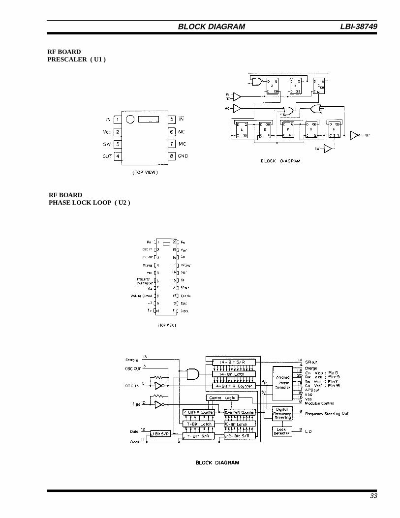
BLOCK DIAGRAM
LCD / KB FLEX BOARDMICRO PROCESSOR ( U1 )
LBI-38749
22

BLOCK DIAGRAM
LCD / KB FLEX LED FLEXAF VOLUME W/SWITCH ( R8 )
SPEAKER( LS1 )
ROTARY SWITCH( S1 )
MICROPHONE W / CAPACITOR( MK1 ) ( C9 )
LBI-38749
23

BLOCK DIAGRAM
CONTROL BOARDMICRO PROCESSOR ( U1 )
CONTROL BOARDMICRO PROCESSOR ( U2 )
LBI-38749
24

BLOCK DIAGRAM
CONTROL BOARDDIGITAL SIGNAL PROCESSOR ( U3 )
CONTROL BOARDFLASH E2PROM ( U4 )
LBI-38749
25

BLOCK DIAGRAM
CONTROL BOARDCMOS SRAM ( U5 )
CONTROL BOARD (AEGIS)FLASH E2PROM ( U4 )28F020
LBI-38749
26

BLOCK DIAGRAM
CONTROL BOARDCMOS SRAM ( U5 )FROM ASSY REV. D
CONTROL BOARD (AEGIS)E2PROM ( U6 )
LBI-38749
27

BLOCK DIAGRAM
CONTROL BOARDAUDIO PROCESSOR ( U7 )
LBI-38749
28

BLOCK DIAGRAM
CONTROL BOARDVOLTAGE REGULATOR ( U9 )
CONTROL BOARDVOLTAGE REGULATOR ( U10 )
CONTROL BOARDINTEGRATED CIRCUIT / AF POWER AMPLIFIER ( U11 )
CONTROL BOARDE2PROM ( U6 )
LBI-38749
29

BLOCK DIAGRAM
CONTROL BOARD2 INPUT OR GATE ( U15 )
CONTROL BOARD3 INVERTERS ( U12 ) ( U20 )
CONTROL BOARDSERIAL NUMBER ( U16 )
RF BOARDBAND PASS FILTER ( FL201 )
CONTROL BOARD ( AEGIS )OP AMP ( U18 ) CONTROL BOARD ( AEGIS )
2 OP AMP ( U18 )FROM ASSY REV. B
LBI-38749
30

BLOCK DIAGRAM
CONTROL BOARD ( AEGIS )ADSP ( U17 ) FROM ASSY REV. B
LBI-38749
31

BLOCK DIAGRAM
RF BOARDBAND PASS FILTER( FL301, FL302 )
CONTROL BOARD ( AEGIS )2 BI-LATERAL SWITCH ( U19 )FROM ASSY REV. B
RF BOARDBAND PASS FILTER( FL305, FL306, FL307 )
LBI-38749
32
BLOCK DIAGRAM
RF BOARDPRESCALER ( U1 )
RF BOARDPHASE LOCK LOOP ( U2 )
LBI-38749
33

BLOCK DIAGRAM
RF BOARDDUAL OP - AMPLIFIER ( U4, U9 )
RF BOARDQUAD / BI - LATERAL SWITCH ( U3 )
LBI-38749
34

BLOCK DIAGRAM
RF BOARDVCO MODULE ( U5 )
RF BOARDREGULATOR ( U6 )
LBI-38749
35

BLOCK DIAGRAM
RF BOARDPOWER AMPLIFIER MODULE ( U7 )
RF BOARDLPF / DC / TR SW MODULE ( U8 )
LBI-38749
36

BLOCK DIAGRAM
RF BOARDIF IC ( U11 )
RF BOARDBI - LATERAL SWITCH ( U12 )
LBI-38749
37

BLOCK DIAGRAM
RF BOARDVC TCXO MODULE ( Z1 )
RF BOARDDOUBLE BALANCED DIODE MIXER ( DBM ) ( Z2 )
LBI-38749
38

BLOCK DIAGRAM
RF BOARD Q102, Q201LED FLEX BOARD Q2
CONTROL BOARD Q3LCD / KB FLEX BOARD Q5 ~ 11
RF BOARD Q105CONTROL BOARD Q8LCD / KB FLEX BOARD Q4
RF BOARD Q205LCD / KB FLEX BOARD Q1, Q3LED FLEX BOARD Q1
CONTROL BOARDQ1, Q5, Q6
CONTROL BOARDQ4, Q7
LBI-38749
39

BLOCK DIAGRAM
RF BOARDQ203 ( VHF, UHF )
RF BOARD Q101, Q103, Q104, Q106, Q107, Q204,Q301 (VHF, UHF), Q302CONTROL BOARD Q2LCD / KB FLEX BOARD Q2
RF BOARD Q202
RF BOARDQ301 ( 800, 900 MHz )
RF BOARDQ203 ( 800, 900 MHz )
CONTROL BOARDCR7 ~ 11, CR12
LBI-38749
40
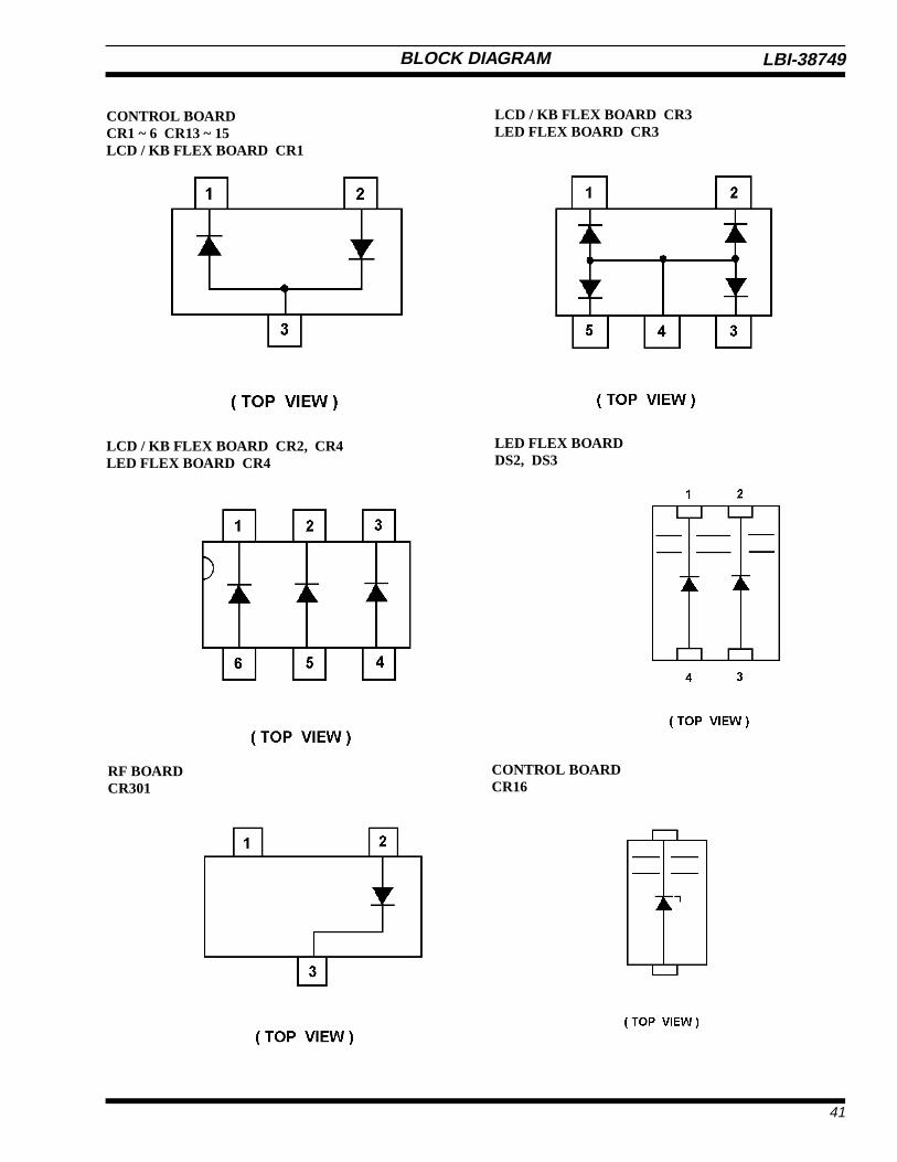
BLOCK DIAGRAM
CONTROL BOARDCR1 ~ 6 CR13 ~ 15LCD / KB FLEX BOARD CR1
LCD / KB FLEX BOARD CR3LED FLEX BOARD CR3
LCD / KB FLEX BOARD CR2, CR4LED FLEX BOARD CR4
LED FLEX BOARDDS2, DS3
RF BOARDCR301
CONTROL BOARDCR16
LBI-38749
41

BLOCK DIAGRAM
LCD / KB FLEX BOARD DS1 ~ 4LED FLEX BOARD DS1
Ericsson Inc.Private Radio SystemsMountain View RoadLynchburg, Virginia 245021-800-528-7711 (Outside USA, 804-528-7711) Printed in U.S.A.
LBI-38749