Embed Size (px)
Citation preview
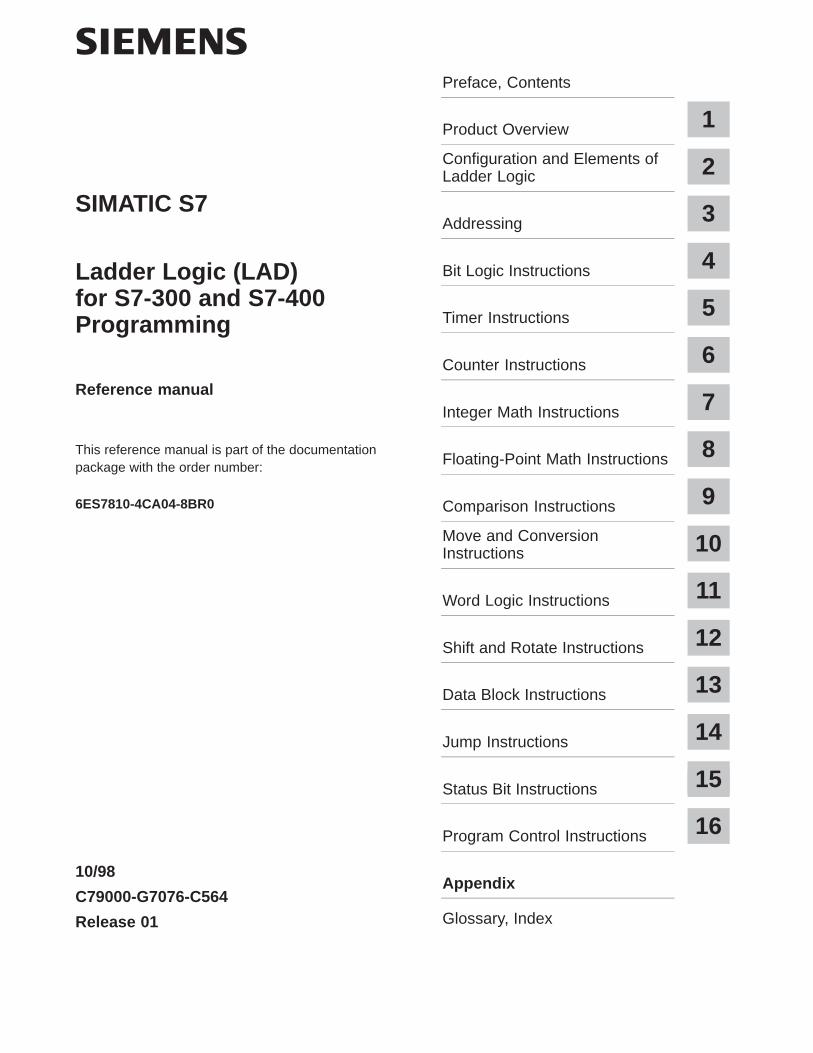
Preface, Contents
Product Overview 1
Configuration and Elements ofLadder Logic 2
Addressing 3
Bit Logic Instructions 4
Timer Instructions 5
Counter Instructions 6
Integer Math Instructions 7
Floating-Point Math Instructions 8
Comparison Instructions 9
Move and ConversionInstructions 10
Word Logic Instructions 11
Shift and Rotate Instructions 12
Data Block Instructions 13
Jump Instructions 14
Status Bit Instructions 15
Program Control Instructions 16
Appendix
Glossary, Index
10/98
C79000-G7076-C564
Release 01
Ladder Logic (LAD) for S7-300 and S7-400Programming
Reference manual
This reference manual is part of the documentation package with the order number:
6ES7810-4CA04-8BR0
SIMATIC S7
iiiLadder Logic (LAD) for S7-300 and S7-400
C79000 G7076 C564 01
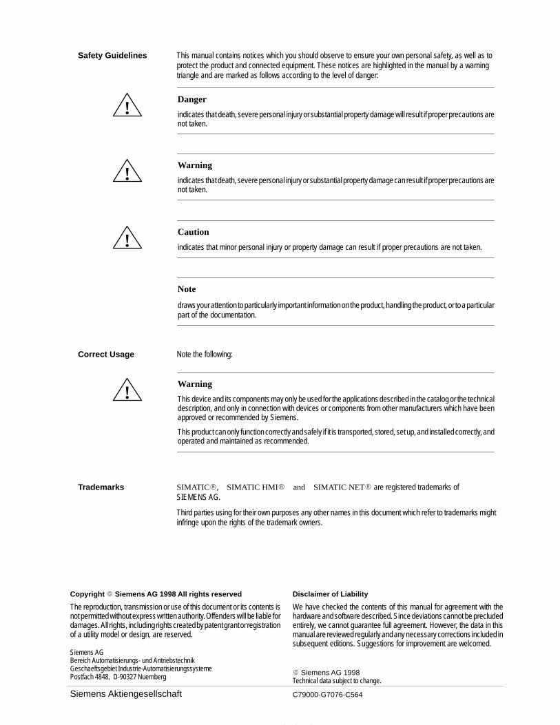
This manual contains notices which you should observe to ensure your own personal safety, as well as toprotect the product and connected equipment. These notices are highlighted in the manual by a warningtriangle and are marked as follows according to the level of danger:
!Danger
indicates that death, severe personal injury or substantial property damage will result if proper precautions arenot taken.
!Warning
indicates that death, severe personal injury or substantial property damage can result if proper precautions arenot taken.
!Caution
indicates that minor personal injury or property damage can result if proper precautions are not taken.
Note
draws your attention to particularly important information on the product, handling the product, or to a particularpart of the documentation.
Note the following:
!Warning
This device and its components may only be used for the applications described in the catalog or the technicaldescription, and only in connection with devices or components from other manufacturers which have beenapproved or recommended by Siemens.
This product can only function correctly and safely if it is transported, stored, set up, and installed correctly, andoperated and maintained as recommended.
SIMATIC�,� SIMATIC HMI�� and� SIMATIC NET� are registered trademarks ofSIEMENS AG.
Third parties using for their own purposes any other names in this document which refer to trademarks mightinfringe upon the rights of the trademark owners.
We have checked the contents of this manual for agreement with thehardware and software described. Since deviations cannot be precludedentirely, we cannot guarantee full agreement. However, the data in thismanual are reviewed regularly and any necessary corrections included insubsequent editions. Suggestions for improvement are welcomed.
� Siemens AG 1998Technical data subject to change.
Disclaimer of LiabilityCopyright � Siemens AG 1998 All rights reserved
The reproduction, transmission or use of this document or its contents isnot permitted without express written authority. Offenders will be liable fordamages. All rights, including rights created by patent grant or registrationof a utility model or design, are reserved.
Siemens AGBereich Automatisierungs- und AntriebstechnikGeschaeftsgebiet Industrie-AutomatisierungssystemePostfach 4848, D-90327 Nuernberg
Siemens Aktiengesellschaft C79000-G7076-C564
Safety Guidelines
Correct Usage
Trademarks
iiiLadder Logic (LAD) for S7-300 and S7-400C79000-G7076-C564-01
Preface
This manual is your guide to creating user programs in the Ladder Logic(LAD) programming language.
This manual also includes a reference section that describes the syntax andfunctions of the language elements of Ladder Logic.
The manual is intended for S7 programmers, operators, andmaintenance/service personnel. A working knowledge of automationprocedures is essential.
This manual is valid for release 5.0 of the STEP 7 programming softwarepackage.
LAD corresponds to the “Ladder Logic” language defined in theInternational Electrotechnical Commission’s standard IEC 1131-3. Forfurther details, refer to the table of standards in the STEP 7 fileNORM_TBL.WRI.
Purpose
Audience
Scope of theManual
Compliance withStandards
ivLadder Logic (LAD) for S7-300 and S7-400
C79000-G7076-C564-01
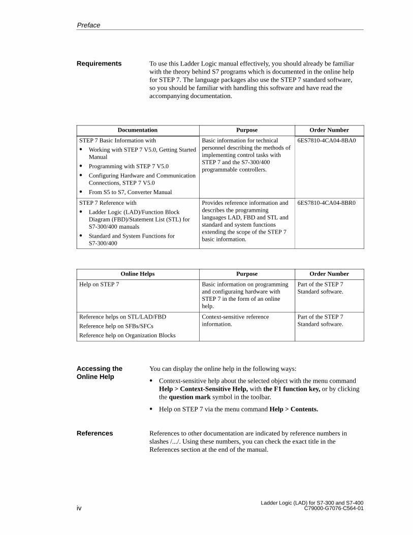
To use this Ladder Logic manual effectively, you should already be familiarwith the theory behind S7 programs which is documented in the online helpfor STEP 7. The language packages also use the STEP 7 standard software,so you should be familiar with handling this software and have read theaccompanying documentation.
Documentation Purpose Order Number
STEP 7 Basic Information with
� Working with STEP 7 V5.0, Getting StartedManual
� Programming with STEP 7 V5.0
� Configuring Hardware and CommunicationConnections, STEP 7 V5.0
� From S5 to S7, Converter Manual
Basic information for technicalpersonnel describing the methods ofimplementing control tasks withSTEP 7 and the S7-300/400programmable controllers.
6ES7810-4CA04-8BA0
STEP 7 Reference with
� Ladder Logic (LAD)/Function BlockDiagram (FBD)/Statement List (STL) forS7-300/400 manuals
� Standard and System Functions forS7-300/400
Provides reference information anddescribes the programminglanguages LAD, FBD and STL andstandard and system functionsextending the scope of the STEP 7basic information.
6ES7810-4CA04-8BR0
Online Helps Purpose Order Number
Help on STEP 7 Basic information on programmingand configuraing hardware withSTEP 7 in the form of an onlinehelp.
Part of the STEP 7Standard software.
Reference helps on STL/LAD/FBD
Reference help on SFBs/SFCs
Reference help on Organization Blocks
Context-sensitive referenceinformation.
Part of the STEP 7Standard software.
You can display the online help in the following ways:
� Context-sensitive help about the selected object with the menu commandHelp > Context-Sensitive Help, with the F1 function key, or by clickingthe question mark symbol in the toolbar.
� Help on STEP 7 via the menu command Help > Contents.
References to other documentation are indicated by reference numbers inslashes /.../. Using these numbers, you can check the exact title in theReferences section at the end of the manual.
Requirements
Accessing theOnline Help
References
Preface
vLadder Logic (LAD) for S7-300 and S7-400C79000-G7076-C564-01
The SIMATIC Customer Support team offers you substantial additionalinformation about SIMATIC products via its online services:
� General current information can be obtained:
– on the Internet underhttp://www.ad.siemens.de/simatic/html_00/simatic
– via the Fax-Polling number 08765-93 02 77 95 00
� Current product information leaflets and downloads which you may finduseful are available:
– on the Internet under http://www.ad.siemens.de/support/html_00/
– via the Bulletin Board System (BBS) in Nuremberg (SIMATICCustomer Support Mailbox) under the number +49 (911) 895-7100.
To dial the mailbox, use a modem with up to V.34 (28.8 Kbps) withthe following parameter settings: 8, N, 1, ANSI; or dial via ISDN(x.75, 64 Kbps).
If you have other questions, please contact the Siemens representative in yourarea. The addresses are listed, for example, in catalogs and in Compuserve(go autforum ).
Our SIMATIC Basic Hotline is also ready to help:
� in Nuremberg, Germany
– Monday to Friday 07:00 to 17:00 (local time): telephone:+49 (911) 895–7000
– or E-mail: [email protected]
� in Johnson City (TN), USA
– Monday to Friday 08:00 to 17:00 (local time): telephone:+1 423 461–2522
– or E-mail: [email protected]
� in Singapore
– Monday to Friday 08:30 to 17:30 (local time): telephone:+65 740–7000
– or E-mail: [email protected]
The SIMATIC Premium Hotline is available round the clock worldwidewith the SIMATIC card (telephone: +49 (911) 895-7777).
Siemens offers a number of training courses to introduce you to the SIMATICS7 automation system. Please contact your regional training center or thecentral training center in Nuremberg, Germany for details:Telephone: +49 (911) 895-3154.
SIMATIC CustomerSupport OnlineServices
AdditionalAssistance
Courses forSIMATIC Products
Preface

viLadder Logic (LAD) for S7-300 and S7-400
C79000-G7076-C564-01
To help us to provide the best possible documentation for you and futureSTEP 7 users, we need your support. If you have any comments orsuggestions relating to this manual or the online help, please complete thequestionnaire at the end of the manual and send it to the address shown.Please include your own personal rating of the documentation.
Questionnaires onthe Manual andOnline Help
Preface
viiLadder Logic (LAD) for S7-300 and S7-400C79000-G7076-C564-01
Contents
Preface iii. . . . . . . . . . . . . . . . . . . . . . . . . . . . . . . . . . . . . . . . . . . . . . . . . . . . . . . . . . . . . . . .
1 Product Overview 1-1. . . . . . . . . . . . . . . . . . . . . . . . . . . . . . . . . . . . . . . . . . . . . . . . . . . . . .
2 Configuration and Elements of Ladder Logic 2-1. . . . . . . . . . . . . . . . . . . . . . . . . . . . .
2.1 Elements and Boxes 2-2. . . . . . . . . . . . . . . . . . . . . . . . . . . . . . . . . . . . . . . . . . . . .
2.2 Boolean Logic and Truth Tables 2-6. . . . . . . . . . . . . . . . . . . . . . . . . . . . . . . . . . .
2.3 Significance of the CPU Registers in Instructions 2-12. . . . . . . . . . . . . . . . . . . .
3 Addressing 3-1. . . . . . . . . . . . . . . . . . . . . . . . . . . . . . . . . . . . . . . . . . . . . . . . . . . . . . . . . . . .
3.1 Overview 3-2. . . . . . . . . . . . . . . . . . . . . . . . . . . . . . . . . . . . . . . . . . . . . . . . . . . . . . .
3.2 Types of Addresses 3-4. . . . . . . . . . . . . . . . . . . . . . . . . . . . . . . . . . . . . . . . . . . . .
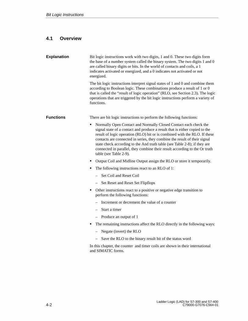
4 Bit Logic Instructions 4-1. . . . . . . . . . . . . . . . . . . . . . . . . . . . . . . . . . . . . . . . . . . . . . . . . . .
4.1 Overview 4-2. . . . . . . . . . . . . . . . . . . . . . . . . . . . . . . . . . . . . . . . . . . . . . . . . . . . . . .
4.2 Normally Open Contact 4-3. . . . . . . . . . . . . . . . . . . . . . . . . . . . . . . . . . . . . . . . . .
4.3 Normally Closed Contact 4-4. . . . . . . . . . . . . . . . . . . . . . . . . . . . . . . . . . . . . . . . .
4.4 Output Coil 4-5. . . . . . . . . . . . . . . . . . . . . . . . . . . . . . . . . . . . . . . . . . . . . . . . . . . . .
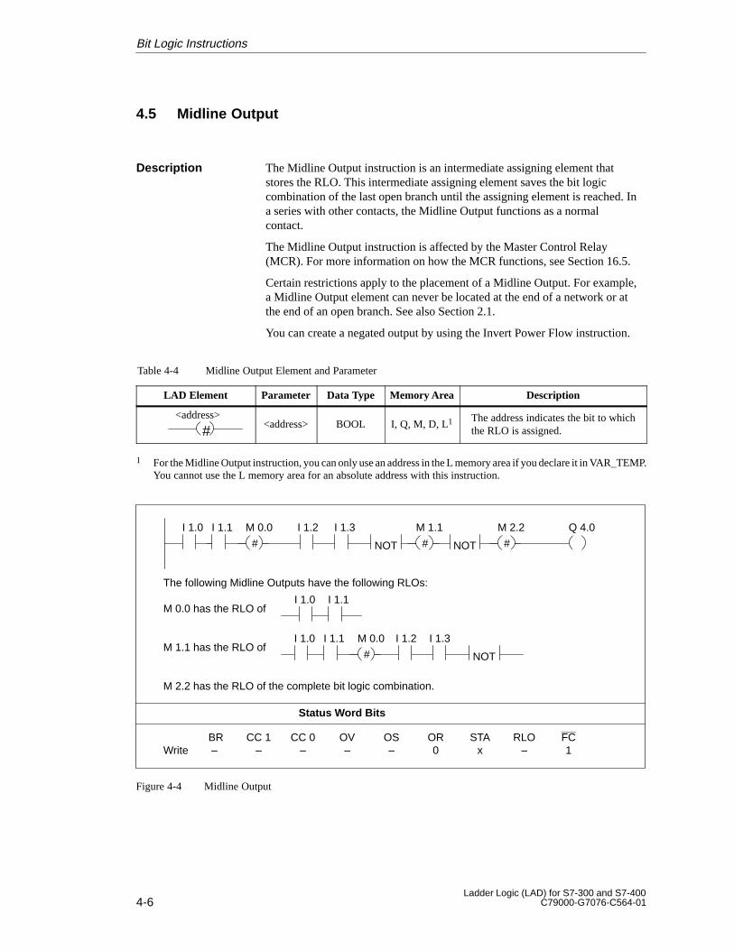
4.5 Midline Output 4-6. . . . . . . . . . . . . . . . . . . . . . . . . . . . . . . . . . . . . . . . . . . . . . . . . .
4.6 Invert Power Flow 4-7. . . . . . . . . . . . . . . . . . . . . . . . . . . . . . . . . . . . . . . . . . . . . . .
4.7 Save RLO to BR Memory 4-8. . . . . . . . . . . . . . . . . . . . . . . . . . . . . . . . . . . . . . . .
4.8 Set Coil 4-9. . . . . . . . . . . . . . . . . . . . . . . . . . . . . . . . . . . . . . . . . . . . . . . . . . . . . . . .
4.9 Reset Coil 4-10. . . . . . . . . . . . . . . . . . . . . . . . . . . . . . . . . . . . . . . . . . . . . . . . . . . . . .
4.10 Set Counter Value 4-11. . . . . . . . . . . . . . . . . . . . . . . . . . . . . . . . . . . . . . . . . . . . . . .
4.11 Up Counter Coil 4-12. . . . . . . . . . . . . . . . . . . . . . . . . . . . . . . . . . . . . . . . . . . . . . . . .
4.12 Down Counter Coil 4-13. . . . . . . . . . . . . . . . . . . . . . . . . . . . . . . . . . . . . . . . . . . . . .
4.13 Pulse Timer Coil 4-14. . . . . . . . . . . . . . . . . . . . . . . . . . . . . . . . . . . . . . . . . . . . . . . .
4.14 Extended Pulse Timer Coil 4-15. . . . . . . . . . . . . . . . . . . . . . . . . . . . . . . . . . . . . . . .
4.15 On-Delay Timer Coil 4-16. . . . . . . . . . . . . . . . . . . . . . . . . . . . . . . . . . . . . . . . . . . . .
4.16 Retentive On-Delay Timer Coil 4-17. . . . . . . . . . . . . . . . . . . . . . . . . . . . . . . . . . . .
4.17 Off-Delay Timer Coil 4-18. . . . . . . . . . . . . . . . . . . . . . . . . . . . . . . . . . . . . . . . . . . . .
4.18 Positive RLO Edge Detection 4-19. . . . . . . . . . . . . . . . . . . . . . . . . . . . . . . . . . . . .
4.19 Negative RLO Edge Detection 4-20. . . . . . . . . . . . . . . . . . . . . . . . . . . . . . . . . . . .
viiiLadder Logic (LAD) for S7-300 and S7-400
C79000-G7076-C564-01
4.20 Address Positive Edge Detection 4-21. . . . . . . . . . . . . . . . . . . . . . . . . . . . . . . . . .
4.21 Address Negative Edge Detection 4-22. . . . . . . . . . . . . . . . . . . . . . . . . . . . . . . . .
4.22 Set Reset Flipflop 4-23. . . . . . . . . . . . . . . . . . . . . . . . . . . . . . . . . . . . . . . . . . . . . . .
4.23 Reset Set Flipflop 4-24. . . . . . . . . . . . . . . . . . . . . . . . . . . . . . . . . . . . . . . . . . . . . . .
5 Timer Instructions 5-1. . . . . . . . . . . . . . . . . . . . . . . . . . . . . . . . . . . . . . . . . . . . . . . . . . . . . .
5.1 Location of a Timer in Memory and Components of a Timer 5-2. . . . . . . . . . .
5.2 Choosing the Right Timer 5-4. . . . . . . . . . . . . . . . . . . . . . . . . . . . . . . . . . . . . . . . .
5.3 Pulse S5 Timer 5-5. . . . . . . . . . . . . . . . . . . . . . . . . . . . . . . . . . . . . . . . . . . . . . . . .
5.4 Extended Pulse S5 Timer 5-7. . . . . . . . . . . . . . . . . . . . . . . . . . . . . . . . . . . . . . . .
5.5 On-Delay S5 Timer 5-9. . . . . . . . . . . . . . . . . . . . . . . . . . . . . . . . . . . . . . . . . . . . . .
5.6 Retentive On-Delay S5 Timer 5-11. . . . . . . . . . . . . . . . . . . . . . . . . . . . . . . . . . . . .
5.7 Off-Delay S5 Timer 5-13. . . . . . . . . . . . . . . . . . . . . . . . . . . . . . . . . . . . . . . . . . . . . .
6 Counter Instructions 6-1. . . . . . . . . . . . . . . . . . . . . . . . . . . . . . . . . . . . . . . . . . . . . . . . . . . .
6.1 Location of a Counter in Memory and Components of a Counter 6-2. . . . . . .
6.2 Up-Down Counter 6-3. . . . . . . . . . . . . . . . . . . . . . . . . . . . . . . . . . . . . . . . . . . . . . .
6.3 Up Counter 6-5. . . . . . . . . . . . . . . . . . . . . . . . . . . . . . . . . . . . . . . . . . . . . . . . . . . . .
6.4 Down Counter 6-7. . . . . . . . . . . . . . . . . . . . . . . . . . . . . . . . . . . . . . . . . . . . . . . . . .
7 Integer Math Instructions 7-1. . . . . . . . . . . . . . . . . . . . . . . . . . . . . . . . . . . . . . . . . . . . . . .
7.1 Add Integer 7-2. . . . . . . . . . . . . . . . . . . . . . . . . . . . . . . . . . . . . . . . . . . . . . . . . . . . .
7.2 Add Double Integer 7-3. . . . . . . . . . . . . . . . . . . . . . . . . . . . . . . . . . . . . . . . . . . . . .
7.3 Subtract Integer 7-4. . . . . . . . . . . . . . . . . . . . . . . . . . . . . . . . . . . . . . . . . . . . . . . . .
7.4 Subtract Double Integer 7-5. . . . . . . . . . . . . . . . . . . . . . . . . . . . . . . . . . . . . . . . . .
7.5 Multiply Integer 7-6. . . . . . . . . . . . . . . . . . . . . . . . . . . . . . . . . . . . . . . . . . . . . . . . .
7.6 Multiply Double Integer 7-7. . . . . . . . . . . . . . . . . . . . . . . . . . . . . . . . . . . . . . . . . . .
7.7 Divide Integer 7-8. . . . . . . . . . . . . . . . . . . . . . . . . . . . . . . . . . . . . . . . . . . . . . . . . . .
7.8 Divide Double Integer 7-9. . . . . . . . . . . . . . . . . . . . . . . . . . . . . . . . . . . . . . . . . . . .
7.9 Return Fraction Double Integer 7-10. . . . . . . . . . . . . . . . . . . . . . . . . . . . . . . . . . . .
7.10 Evaluating the Bits of the Status Word After Integer Math Instructions 7-11. .
8 Floating-Point Math Instructions 8-1. . . . . . . . . . . . . . . . . . . . . . . . . . . . . . . . . . . . . . . . .
8.1 Overview 8-2. . . . . . . . . . . . . . . . . . . . . . . . . . . . . . . . . . . . . . . . . . . . . . . . . . . . . . .
8.2 Add Floating-Point Numbers 8-3. . . . . . . . . . . . . . . . . . . . . . . . . . . . . . . . . . . . . .
8.3 Subtract Floating-Point Numbers 8-4. . . . . . . . . . . . . . . . . . . . . . . . . . . . . . . . . .
8.4 Multiply Floating-Point Numbers 8-5. . . . . . . . . . . . . . . . . . . . . . . . . . . . . . . . . . .
8.5 Divide Floating-Point Numbers 8-6. . . . . . . . . . . . . . . . . . . . . . . . . . . . . . . . . . . .
8.6 Evaluating the Bits of the Status Word After Floating-Point Instructions 8-7.
Contents
ixLadder Logic (LAD) for S7-300 and S7-400C79000-G7076-C564-01
8.7 Establishing the Absolute Value of a Floating-Point Number 8-8. . . . . . . . . . .
8.8 Establishing the Square and/or the Square Root of a Floating-Point Number 8-9. . . . . . . . . . . . . . . . . . . . . . . . . . . . . . . . . . . . . . . . . . .
8.9 Establishing the Natural Logarithm of a Floating-Point Number 8-11. . . . . . . .
8.10 Establishing the Exponential Value of a Floating-Point Number 8-12. . . . . . . .
8.11 Establishing the Trigonometrical Functions of Angles as Floating-Point Numbers 8-13. . . . . . . . . . . . . . . . . . . . . . . . . . . . . . . . . . . . . . . . . .
9 Comparison Instructions 9-1. . . . . . . . . . . . . . . . . . . . . . . . . . . . . . . . . . . . . . . . . . . . . . . .
9.1 Compare Integer 9-2. . . . . . . . . . . . . . . . . . . . . . . . . . . . . . . . . . . . . . . . . . . . . . . .
9.2 Compare Double Integer 9-3. . . . . . . . . . . . . . . . . . . . . . . . . . . . . . . . . . . . . . . . .
9.3 Compare Floating-Point Numbers 9-5. . . . . . . . . . . . . . . . . . . . . . . . . . . . . . . . .
10 Move and Conversion Instructions 10-1. . . . . . . . . . . . . . . . . . . . . . . . . . . . . . . . . . . . . . .
10.1 Assign a Value 10-2. . . . . . . . . . . . . . . . . . . . . . . . . . . . . . . . . . . . . . . . . . . . . . . . . .
10.2 BCD to Integer 10-4. . . . . . . . . . . . . . . . . . . . . . . . . . . . . . . . . . . . . . . . . . . . . . . . . .
10.3 Integer to BCD 10-5. . . . . . . . . . . . . . . . . . . . . . . . . . . . . . . . . . . . . . . . . . . . . . . . . .
10.4 Integer to Double Integer 10-6. . . . . . . . . . . . . . . . . . . . . . . . . . . . . . . . . . . . . . . . .
10.5 BCD to Double Integer 10-7. . . . . . . . . . . . . . . . . . . . . . . . . . . . . . . . . . . . . . . . . . .
10.6 Double Integer to BCD 10-8. . . . . . . . . . . . . . . . . . . . . . . . . . . . . . . . . . . . . . . . . . .
10.7 Double Integer to Floating-Point Number 10-9. . . . . . . . . . . . . . . . . . . . . . . . . . .
10.8 Ones Complement Integer 10-10. . . . . . . . . . . . . . . . . . . . . . . . . . . . . . . . . . . . . . . .
10.9 Ones Complement Double Integer 10-11. . . . . . . . . . . . . . . . . . . . . . . . . . . . . . . . .
10.10 Twos Complement Integer 10-12. . . . . . . . . . . . . . . . . . . . . . . . . . . . . . . . . . . . . . . .
10.11 Twos Complement Double Integer 10-13. . . . . . . . . . . . . . . . . . . . . . . . . . . . . . . . .
10.12 Negate Floating-Point Number 10-14. . . . . . . . . . . . . . . . . . . . . . . . . . . . . . . . . . . .
10.13 Round to Double Integer 10-15. . . . . . . . . . . . . . . . . . . . . . . . . . . . . . . . . . . . . . . . .
10.14 Truncate Double Integer Part 10-16. . . . . . . . . . . . . . . . . . . . . . . . . . . . . . . . . . . . .
10.15 Ceiling 10-17. . . . . . . . . . . . . . . . . . . . . . . . . . . . . . . . . . . . . . . . . . . . . . . . . . . . . . . . .
10.16 Floor 10-18. . . . . . . . . . . . . . . . . . . . . . . . . . . . . . . . . . . . . . . . . . . . . . . . . . . . . . . . . .
11 Word Logic Instructions 11-1. . . . . . . . . . . . . . . . . . . . . . . . . . . . . . . . . . . . . . . . . . . . . . . .
11.1 Overview 11-2. . . . . . . . . . . . . . . . . . . . . . . . . . . . . . . . . . . . . . . . . . . . . . . . . . . . . . .
11.2 WAnd Word 11-3. . . . . . . . . . . . . . . . . . . . . . . . . . . . . . . . . . . . . . . . . . . . . . . . . . . .
11.3 WAnd Double Word 11-4. . . . . . . . . . . . . . . . . . . . . . . . . . . . . . . . . . . . . . . . . . . . . .
11.4 WOr Word 11-5. . . . . . . . . . . . . . . . . . . . . . . . . . . . . . . . . . . . . . . . . . . . . . . . . . . . . .
11.5 WOr Double Word 11-6. . . . . . . . . . . . . . . . . . . . . . . . . . . . . . . . . . . . . . . . . . . . . . .
11.6 WXOr Word 11-7. . . . . . . . . . . . . . . . . . . . . . . . . . . . . . . . . . . . . . . . . . . . . . . . . . . .
11.7 WXOr Double Word 11-8. . . . . . . . . . . . . . . . . . . . . . . . . . . . . . . . . . . . . . . . . . . . .
Contents
xLadder Logic (LAD) for S7-300 and S7-400
C79000-G7076-C564-01
12 Shift and Rotate Instructions 12-1. . . . . . . . . . . . . . . . . . . . . . . . . . . . . . . . . . . . . . . . . . . .
12.1 Shift Instructions 12-2. . . . . . . . . . . . . . . . . . . . . . . . . . . . . . . . . . . . . . . . . . . . . . . .
12.2 Rotate Instructions 12-10. . . . . . . . . . . . . . . . . . . . . . . . . . . . . . . . . . . . . . . . . . . . . .
13 Data Block Instructions 13-1. . . . . . . . . . . . . . . . . . . . . . . . . . . . . . . . . . . . . . . . . . . . . . . . .
13.1 Open Data Block: DB or DI 13-2. . . . . . . . . . . . . . . . . . . . . . . . . . . . . . . . . . . . . . .
14 Jump Instructions 14-1. . . . . . . . . . . . . . . . . . . . . . . . . . . . . . . . . . . . . . . . . . . . . . . . . . . . . .
14.1 Overview 14-2. . . . . . . . . . . . . . . . . . . . . . . . . . . . . . . . . . . . . . . . . . . . . . . . . . . . . . .
14.2 Jump in the Block If RLO = 1 (Unconditional Jump) 14-3. . . . . . . . . . . . . . . . . .
14.3 Jump in the Block If RLO = 1 (Conditional Jump) 14-4. . . . . . . . . . . . . . . . . . . .
14.4 Jump in the Block If RLO = 0 (Jump-If-Not) 14-5. . . . . . . . . . . . . . . . . . . . . . . . .
14.5 Label 14-6. . . . . . . . . . . . . . . . . . . . . . . . . . . . . . . . . . . . . . . . . . . . . . . . . . . . . . . . . .
15 Status Bit Instructions 15-1. . . . . . . . . . . . . . . . . . . . . . . . . . . . . . . . . . . . . . . . . . . . . . . . . .
15.1 Overview 15-2. . . . . . . . . . . . . . . . . . . . . . . . . . . . . . . . . . . . . . . . . . . . . . . . . . . . . . .
15.2 Exception Bit BR Memory 15-3. . . . . . . . . . . . . . . . . . . . . . . . . . . . . . . . . . . . . . . .
15.3 Result Bits 15-4. . . . . . . . . . . . . . . . . . . . . . . . . . . . . . . . . . . . . . . . . . . . . . . . . . . . .
15.4 Exception Bits Unordered 15-6. . . . . . . . . . . . . . . . . . . . . . . . . . . . . . . . . . . . . . . .
15.5 Exception Bit Overflow 15-7. . . . . . . . . . . . . . . . . . . . . . . . . . . . . . . . . . . . . . . . . . .
15.6 Exception Bit Overflow Stored 15-9. . . . . . . . . . . . . . . . . . . . . . . . . . . . . . . . . . . .
16 Program Control Instructions 16-1. . . . . . . . . . . . . . . . . . . . . . . . . . . . . . . . . . . . . . . . . . .
16.1 Calling FCs/SFCs from Coil 16-2. . . . . . . . . . . . . . . . . . . . . . . . . . . . . . . . . . . . . . .
16.2 Calling FBs, FCs, SFBs, SFCs, and Multiple Instances 16-4. . . . . . . . . . . . . . .
16.3 Return 16-8. . . . . . . . . . . . . . . . . . . . . . . . . . . . . . . . . . . . . . . . . . . . . . . . . . . . . . . . .
Important Notes on Using MCR Functions 16-9. . . . . . . . . . . . . . . . . . . . . . . . . .
16.4 Master Control Relay Instructions 16-10. . . . . . . . . . . . . . . . . . . . . . . . . . . . . . . . . .
16.5 Master Control Relay Activate/Deactivate 16-11. . . . . . . . . . . . . . . . . . . . . . . . . . .
16.6 Master Control Relay On/Off 16-14. . . . . . . . . . . . . . . . . . . . . . . . . . . . . . . . . . . . . .
A Alphabetical Listing of Instructions A-1. . . . . . . . . . . . . . . . . . . . . . . . . . . . . . . . . . . . . .
A.1 Listing with International Names A-2. . . . . . . . . . . . . . . . . . . . . . . . . . . . . . . . . . .
A.2 Listing with International Names and SIMATIC Equivalents A-5. . . . . . . . . . . .
A.3 Listing with SIMATIC Names A-9. . . . . . . . . . . . . . . . . . . . . . . . . . . . . . . . . . . . . .
A.4 Listing with SIMATIC Names and International Equivalents A-12. . . . . . . . . . . .
A.5 Listing with International Short Names and SIMATIC Short Names A-16. . . . .
B Programming Examples B-1. . . . . . . . . . . . . . . . . . . . . . . . . . . . . . . . . . . . . . . . . . . . . . . . .
B.1 Overview B-2. . . . . . . . . . . . . . . . . . . . . . . . . . . . . . . . . . . . . . . . . . . . . . . . . . . . . . .
B.2 Bit Logic Instructions B-3. . . . . . . . . . . . . . . . . . . . . . . . . . . . . . . . . . . . . . . . . . . . .
Contents
xiLadder Logic (LAD) for S7-300 and S7-400C79000-G7076-C564-01
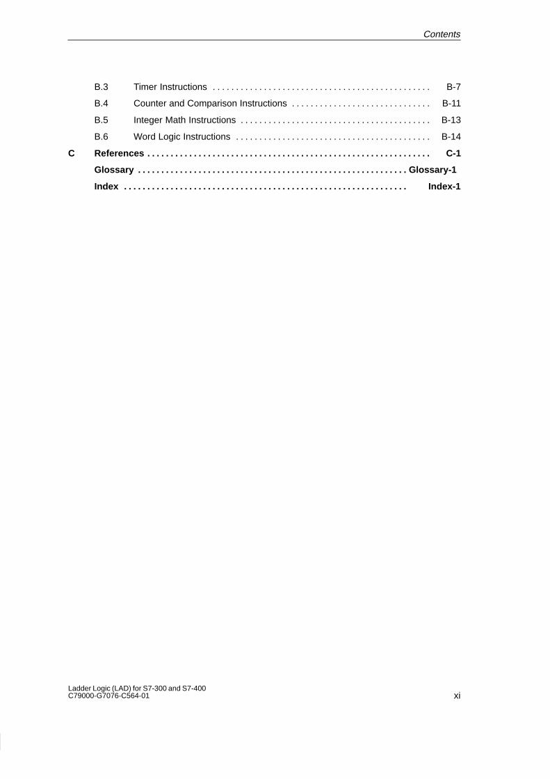
B.3 Timer Instructions B-7. . . . . . . . . . . . . . . . . . . . . . . . . . . . . . . . . . . . . . . . . . . . . . .
B.4 Counter and Comparison Instructions B-11. . . . . . . . . . . . . . . . . . . . . . . . . . . . . .
B.5 Integer Math Instructions B-13. . . . . . . . . . . . . . . . . . . . . . . . . . . . . . . . . . . . . . . . .
B.6 Word Logic Instructions B-14. . . . . . . . . . . . . . . . . . . . . . . . . . . . . . . . . . . . . . . . . .
C References C-1. . . . . . . . . . . . . . . . . . . . . . . . . . . . . . . . . . . . . . . . . . . . . . . . . . . . . . . . . . . . .
Glossary Glossary-1. . . . . . . . . . . . . . . . . . . . . . . . . . . . . . . . . . . . . . . . . . . . . . . . . . . . . . . . . .
Index Index-1. . . . . . . . . . . . . . . . . . . . . . . . . . . . . . . . . . . . . . . . . . . . . . . . . . . . . . . . . . . . .
Contents

xiiLadder Logic (LAD) for S7-300 and S7-400
C79000-G7076-C564-01
Contents
1-1Ladder Logic (LAD) for S7-300 and S7-400C79000-G7076-C564-01
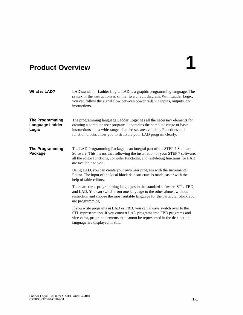
Product Overview
LAD stands for Ladder Logic. LAD is a graphic programming language. Thesyntax of the instructions is similar to a circuit diagram. With Ladder Logic,you can follow the signal flow between power rails via inputs, outputs, andinstructions.
The programming language Ladder Logic has all the necessary elements forcreating a complete user program. It contains the complete range of basicinstructions and a wide range of addresses are available. Functions andfunction blocks allow you to structure your LAD program clearly.
The LAD Programming Package is an integral part of the STEP 7 StandardSoftware. This means that following the installation of your STEP 7 software,all the editor functions, compiler functions, and test/debug functions for LADare available to you.
Using LAD, you can create your own user program with the IncrementalEditor. The input of the local block data structure is made easier with thehelp of table editors.
There are three programming languages in the standard software, STL, FBD,and LAD. You can switch from one language to the other almost withoutrestriction and choose the most suitable language for the particular block youare programming.
If you write programs in LAD or FBD, you can always switch over to theSTL representation. If you convert LAD programs into FBD programs andvice versa, program elements that cannot be represented in the destinationlanguage are displayed in STL.
What is LAD?
The ProgrammingLanguage LadderLogic
The ProgrammingPackage
1

1-2Ladder Logic (LAD) for S7-300 and S7-400
C79000-G7076-C564-01
2-1Ladder Logic (LAD) for S7-300 and S7-400C79000-G7076-C564-01
Configuration and Elements of LadderLogic
Section Description Page
2.1 Elements and Box Structure 2-2
2.2 Boolean Logic and Truth Tables 2-6
2.3 Significance of the CPU Registers in Instructions 2-12
Chapter Overview
2
2-2Ladder Logic (LAD) for S7-300 and S7-400
C79000-G7076-C564-01
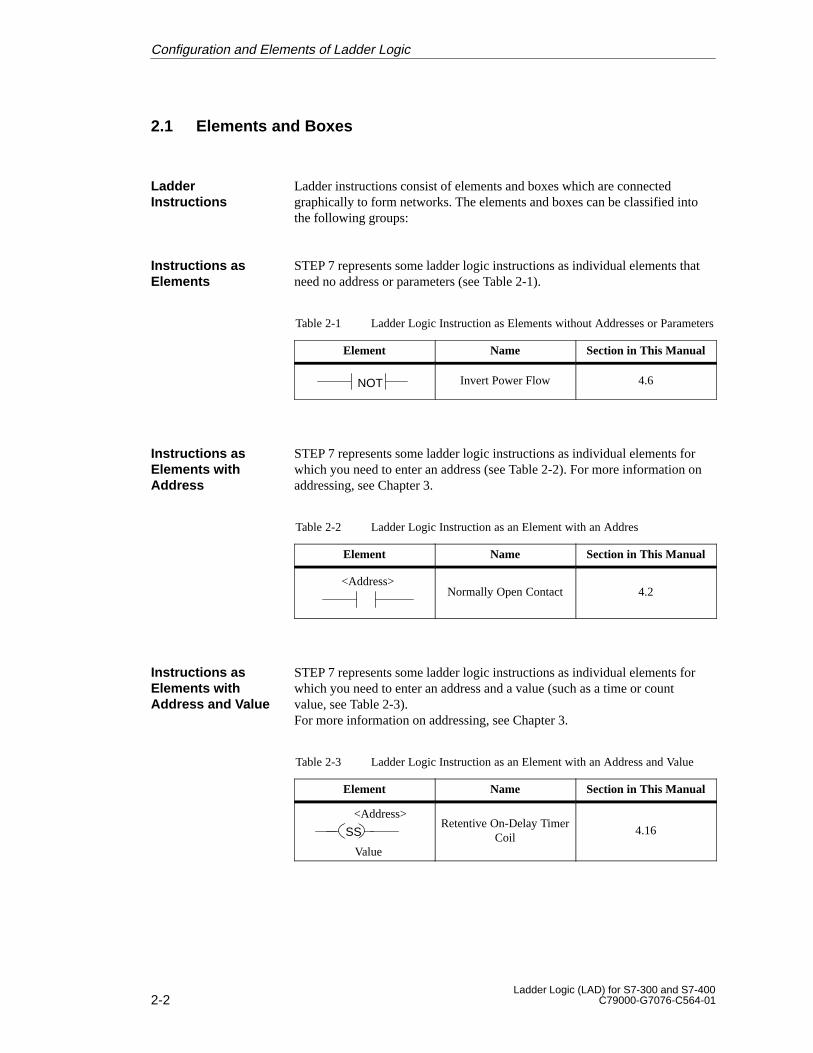
2.1 Elements and Boxes
Ladder instructions consist of elements and boxes which are connectedgraphically to form networks. The elements and boxes can be classified intothe following groups:
STEP 7 represents some ladder logic instructions as individual elements thatneed no address or parameters (see Table 2-1).
Table 2-1 Ladder Logic Instruction as Elements without Addresses or Parameters
Element Name Section in This Manual
NOT Invert Power Flow 4.6
STEP 7 represents some ladder logic instructions as individual elements forwhich you need to enter an address (see Table 2-2). For more information onaddressing, see Chapter 3.
Table 2-2 Ladder Logic Instruction as an Element with an Addres
Element Name Section in This Manual
<Address>Normally Open Contact 4.2
STEP 7 represents some ladder logic instructions as individual elements forwhich you need to enter an address and a value (such as a time or countvalue, see Table 2-3).For more information on addressing, see Chapter 3.
Table 2-3 Ladder Logic Instruction as an Element with an Address and Value
Element Name Section in This Manual
SS
<Address>
Value
Retentive On-Delay TimerCoil
4.16
LadderInstructions
Instructions asElements
Instructions asElements withAddress
Instructions asElements withAddress and Value
Configuration and Elements of Ladder Logic

2-3Ladder Logic (LAD) for S7-300 and S7-400C79000-G7076-C564-01
STEP 7 represents some ladder logic instructions as boxes with linesindicating inputs and outputs (see Table 2-4). The inputs are on the left sideof the box; the outputs are on the right side of the box. You fill in the inputparameters. For the output parameters, you fill in locations where the STEP 7software can place output information for you. You must use the specificnotation of the individual data types for the parameters.
The principle of the enable in (EN) and enable out (ENO) parameters isexplained below. For more information on input and output parameters, seethe description of each instruction in this manual.
Table 2-4 Ladder Logic Instruction as Box with Inputs and Outputs
Box Name Section in This Manual
DIV_R
IN1
EN
IN2 OUT
ENODivide Real 8.5
Passing power to (activating) the enable input (EN) of a ladder logic boxcauses the box to carry out a specific function. If the box is able to executeits function without error, the enable output (ENO) passes power along thecircuit. The ladder logic box parameters EN and ENO are of data type BOOLand can be in memory area I, Q, M, D, or L (see Tables 2-5 and 2-6).
EN and ENO function according to the following principles:
� If EN is not activated (that is, if it has a signal state of 0), the box doesnot carry out its function and ENO is not activated (that is, it also has asignal state of 0).
� If EN is activated (that is, if it has a signal state of 1) and the box towhich EN belongs executes its function without error, ENO is alsoactivated (that is, it also has a signal state of 1).
� If EN is activated (that is, if it has a signal state of 1) and an error occurswhile the box to which EN belongs is executing its function, ENO is notactivated (that is, its signal state is 0).
You cannot place a box or an inline coil in a ladder logic rung which does notstart at the left power rail. The Compare instructions are an exception.
Most of the addresses in LAD relate to memory areas. The following tableshows the types and their functions.
Instructions asBoxes withParameters
Enable In andEnable OutParameters
Restrictions forBoxes and InlineCoils
Memory Areas andTheir Functions
Configuration and Elements of Ladder Logic
2-4Ladder Logic (LAD) for S7-300 and S7-400
C79000-G7076-C564-01
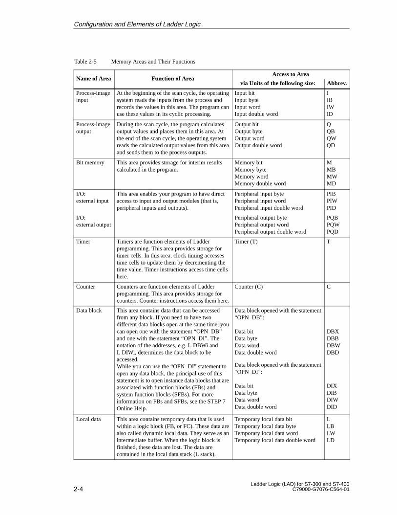
Table 2-5 Memory Areas and Their Functions
Name of Area Function of AreaAccess to Area
Name of Ar ea Function of Ar eavia Units of the following size: Abbrev.
Process-imageinput
At the beginning of the scan cycle, the operatingsystem reads the inputs from the process andrecords the values in this area. The program canuse these values in its cyclic processing.
Input bitInput byteInput wordInput double word
IIBIWID
Process-imageoutput
During the scan cycle, the program calculatesoutput values and places them in this area. Atthe end of the scan cycle, the operating systemreads the calculated output values from this areaand sends them to the process outputs.
Output bitOutput byteOutput wordOutput double word
QQBQWQD
Bit memory This area provides storage for interim resultscalculated in the program.
Memory bitMemory byteMemory wordMemory double word
MMBMWMD
I/O:external input
This area enables your program to have directaccess to input and output modules (that is,peripheral inputs and outputs).
Peripheral input bytePeripheral input wordPeripheral input double word
PIBPIWPID
I/O:external output
Peripheral output bytePeripheral output wordPeripheral output double word
PQBPQWPQD
Timer Timers are function elements of Ladderprogramming. This area provides storage fortimer cells. In this area, clock timing accessestime cells to update them by decrementing thetime value. Timer instructions access time cellshere.
Timer (T) T
Counter Counters are function elements of Ladderprogramming. This area provides storage forcounters. Counter instructions access them here.
Counter (C) C
Data block This area contains data that can be accessedfrom any block. If you need to have twodifferent data blocks open at the same time, youcan open one with the statement “OPN DB”and one with the statement “OPN DI”. Thenotation of the addresses, e.g. L DBWi andL DIWi, determines the data block to beaccessed.
Data block opened with the statement“OPN DB”:
Data bitData byteData wordData double word
DBXDBBDBWDBD
accessed.While you can use the “OPN DI” statement toopen any data block, the principal use of thisstatement is to open instance data blocks that areassociated with function blocks (FBs) andsystem function blocks (SFBs). For moreinformation on FBs and SFBs, see the STEP 7Online Help.
Data block opened with the statement“OPN DI”:
Data bitData byteData wordData double word
DIXDIBDIWDID
Local data This area contains temporary data that is usedwithin a logic block (FB, or FC). These data arealso called dynamic local data. They serve as anintermediate buffer. When the logic block isfinished, these data are lost. The data arecontained in the local data stack (L stack).
Temporary local data bitTemporary local data byteTemporary local data wordTemporary local data double word
LLBLWLD
Configuration and Elements of Ladder Logic
2-5Ladder Logic (LAD) for S7-300 and S7-400C79000-G7076-C564-01
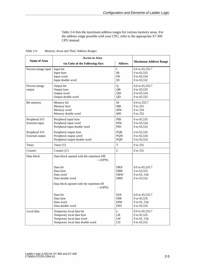
Table 2-6 lists the maximum address ranges for various memory areas. Forthe address range possible with your CPU, refer to the appropriate S7-300CPU manual.
Table 2-6 Memory Areas and Their Address Ranges
Name of AreaAccess to Area
Maximum Address RangeName of Areavia Units of the Following Size: Abbrev.
Maximum Address Range
Process-image inputInput bitInput byteInput wordInput double word
IIBIWID
0.0 to 65,535.70 to 65,5350 to 65,5340 to 65,532
Process-imageoutput
Output bitOutput byteOutput wordOutput double word
QQBQWQD
0.0 to 65,535.70 to 65,5350 to 65,5340 to 65,532
Bit memory Memory bitMemory byteMemory wordMemory double word
MMBMWMD
0.0 to 255.70 to 2550 to 2540 to 252
Peripheral I/O:External input
Peripheral input bytePeripheral input wordPeripheral input double word
PIBPIWPID
0 to 65,5350 to 65,5340 to 65,532
Peripheral I/O:External output
Peripheral output bytePeripheral output wordPeripheral output double word
PQBPQWPQD
0 to 65,5350 to 65,5340 to 65,532
Timer Timer (T) T 0 to 255
Counter Counter (C) C 0 to 255
Data block Data block opened with the statement DB ––(OPN)
Data bitData byteData wordData double word
DBXDBBDBWDBD
0.0 to 65,535.70 to 65,5350 to 65, 5340 to 65,532
Data block opened with the statement DI ––(OPN)
Data bitData byteData wordData double word
DIXDIBDIWDID
0.0 to 65,535.70 to 65,5350 to 65, 5340 to 65,532
Local data Temporary local data bitTemporary local data byteTemporary local data wordTemporary local data double word
LLBLWLD
0.0 to 65,535.70 to 65,5350 to 65, 5340 to 65,532
Configuration and Elements of Ladder Logic
2-6Ladder Logic (LAD) for S7-300 and S7-400
C79000-G7076-C564-01
2.2 Boolean Logic and Truth Tables
A ladder logic program tracks power flow between power rails as it passesthrough various inputs, outputs, and other elements and boxes. Many Ladderinstructions work according to the principles of Boolean logic.
Each of the Boolean logic instructions checks the signal state of an electricalcontact for 0 (not activated, off) or 1 (activated, on) and produces a resultbased on the findings. The instruction then either stores this result or uses itto perform a Boolean logic operation. The result of the logic operation iscalled the RLO. The principles of Boolean logic are demonstrated here onthe basis of normally open and normally closed contacts.
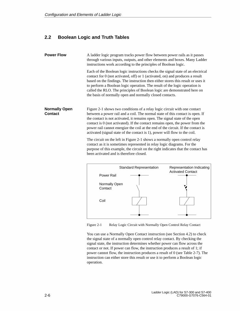
Figure 2-1 shows two conditions of a relay logic circuit with one contactbetween a power rail and a coil. The normal state of this contact is open. Ifthe contact is not activated, it remains open. The signal state of the opencontact is 0 (not activated). If the contact remains open, the power from thepower rail cannot energize the coil at the end of the circuit. If the contact isactivated (signal state of the contact is 1), power will flow to the coil.
The circuit on the left in Figure 2-1 shows a normally open control relaycontact as it is sometimes represented in relay logic diagrams. For thepurpose of this example, the circuit on the right indicates that the contact hasbeen activated and is therefore closed.
Power Rail
Normally OpenContact
Coil
ÍÍ
Standard Representation Representation IndicatingActivated Contact
Figure 2-1 Relay Logic Circuit with Normally Open Control Relay Contact
You can use a Normally Open Contact instruction (see Section 4.2) to checkthe signal state of a normally open control relay contact. By checking thesignal state, the instruction determines whether power can flow across thecontact or not. If power can flow, the instruction produces a result of 1; ifpower cannot flow, the instruction produces a result of 0 (see Table 2-7). Theinstruction can either store this result or use it to perform a Boolean logicoperation.
Power Flow
Normally OpenContact
Configuration and Elements of Ladder Logic
2-7Ladder Logic (LAD) for S7-300 and S7-400C79000-G7076-C564-01
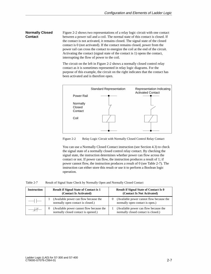
Figure 2-2 shows two representations of a relay logic circuit with one contactbetween a power rail and a coil. The normal state of this contact is closed. Ifthe contact is not activated, it remains closed. The signal state of the closedcontact is 0 (not activated). If the contact remains closed, power from thepower rail can cross the contact to energize the coil at the end of the circuit.Activating the contact (signal state of the contact is 1) opens the contact,interrupting the flow of power to the coil.
The circuit on the left in Figure 2-2 shows a normally closed control relaycontact as it is sometimes represented in relay logic diagrams. For thepurpose of this example, the circuit on the right indicates that the contact hasbeen activated and is therefore open.
Power Rail
NormallyClosedContact
Coil
Standard Representation Representation IndicatingActivated Contact
Figure 2-2 Relay Logic Circuit with Normally Closed Control Relay Contact
You can use a Normally Closed Contact instruction (see Section 4.3) to checkthe signal state of a normally closed control relay contact. By checking thesignal state, the instruction determines whether power can flow across thecontact or not. If power can flow, the instruction produces a result of 1; ifpower cannot flow, the instruction produces a result of 0 (see Table 2-7). Theinstruction can either store this result or use it to perform a Boolean logicoperation.
Table 2-7 Result of Signal State Check by Normally Open and Normally Closed Contact
Instruction Result if Signal State of Contact is 1(Contact Is Activated)
Result if Signal State of Contact Is 0(Contact Is Not Activated)
1 (Available power can flow because thenormally open contact is closed.)
0 (Available power cannot flow because thenormally open contact is open.)
0 (Available power cannot flow because thenormally closed contact is opened.)
1 (Available power can flow because thenormally closed contact is closed.)
Normally ClosedContact
Configuration and Elements of Ladder Logic
2-8Ladder Logic (LAD) for S7-300 and S7-400
C79000-G7076-C564-01
Figure 2-3 shows a logic string of Ladder instructions that represents twonormally open contacts connected in series to a coil. The contacts arelabelled “I” for “input” and the coil is labelled “Q” for “output.” Activating anormally open contact closes the contact. When both contacts in the logicstring are activated (that is, closed), power can flow from the power railacross each contact to energize the coil at the end of the circuit. That is,when both contact I 1.0 and I 1.1 are activated, power can flow to the coil.
In Diagram 1, both contacts are activated. Activating a normally opencontact closes the contact. Power can flow from the power rail across eachclosed contact to energize the coil at the end of the circuit.
In Diagrams 2 and 3, because one of the two contacts is not activated, powercannot flow all the way to the coil. The coil is not energized.
In Diagram 4, neither contact is activated. Both contacts remain open. Powercannot flow to the coil. The coil is not energized.
I 1.0 I 1.1 Q 4.0
Diagram 1 Diagram 2
Diagram 3 Diagram 4
= activated = energized
I 1.0 I 1.1 Q 4.0
I 1.0 I 1.1 Q 4.0 I 1.0 I 1.1 Q 4.0
Figure 2-3 Using Normally Open Contact to Program Contacts in a Series
ProgrammingContacts in Series
Configuration and Elements of Ladder Logic
2-9Ladder Logic (LAD) for S7-300 and S7-400C79000-G7076-C564-01
Figure 2-3 shows a ladder logic diagram that you can use to program twonormally open contacts connected in series to a coil. The first Normally OpenContact instruction in the logic string checks the signal state of the firstcontact in the series (input I 1.0) and produces a result based on the findings(see Table 2-7). This result can be 1 or 0. A result of 1 means that the contactis closed and any available power could flow across the contact; a result of 0means that the contact is open, interrupting the flow of any power availableat the contact. The first Normally Open Contact instruction copies this 1 or 0to a memory bit in the status word of the programmable logic controller. Thisbit is called the “result of logic operation” (RLO) bit.
The second Normally Open Contact instruction in the logic string checks thesignal state of the second contact in the series (I 1.1) and produces a resultbased on the findings (see Table 2-7). This result can be 1 or 0, depending onwhether the contact is closed or open. At this point, the second NormallyOpen Contact instruction performs a Boolean logic combination. Theinstruction takes the result it produced upon checking the signal state of thesecond contact and combines this result with the value stored in the RLO bit.The result of this combination (either 1 or 0) is stored in the RLO bit of thestatus word, replacing the old value stored there. The Output Coil instruction(see Section 4.4) assigns this new value to the coil (output Q 4.0).
The possible results of such a logic combination can be shown in a “truthtable.” In such a logic combination, 1 represents “true” and 0 represents“false.” The possible Boolean logic combinations and their results aresummed up in Table 2-8, where “contact is closed” and “power can flow”correspond to “true” and “contact is open” and “power cannot flow”correspond to “false” (see Figure 2-3 for the contacts).
Table 2-8 Truth Table: And
If the result produced bychecking the signal stateof contact I 1.0 is
and the result producedby checking the signalstate of contact I 1.1 is
the result of the logicoperation shown inFigure 2-3 is
1 (contact is closed) 1 (contact is closed) 1 (power can flow)
0 (contact is open) 1 (contact is closed) 0 (power cannot flow)
1 (contact is closed) 0 (contact is open) 0 (power cannot flow)
0 (contact is open) 0 (contact is open) 0 (power cannot flow)
Using NormallyOpen Contact inSeries
Configuration and Elements of Ladder Logic
2-10Ladder Logic (LAD) for S7-300 and S7-400
C79000-G7076-C564-01
Figure 2-4 shows a logic string of Ladder instructions that represent twonormally open contacts connected in parallel to a coil. The contacts arelabelled “I” for “input” and the coil is labelled “Q” for “output.” Activating anormally open contact closes the contact. When either one contact in thelogic string (I 1.1) or the other contact in the logic string (I 1.0) is activated(that is, closed), power can flow from the power rail to energize the coil(Q 4.0) at the end of the circuit. If both contacts in the logic string areactivated, power can flow from the power rail to energize the coil.
In Diagrams 1 and 2, one contact is activated and the other is not. Activatinga normally open contact closes the contact. Power can flow from the powerrail across the closed contact and continue to the coil at the end of the circuit.Because the two contacts are connected in parallel, only one of the twocontacts need be closed for the power flow to continue to the coil at the endof the circuit to energize the coil.
In Diagram 3, both contacts are activated, enabling the power to flow acrossthe two closed contacts to the end of the circuit to energize the coil.
In Diagram 4, neither contact is activated. Both contacts remain open. Powercannot flow to the coil. The coil is not energized.
I 1.1
I 1.1
Diagram 1 Diagram 2
Diagram 3 Diagram 4
= activated = energized
I 1.0 Q 4.0
I 1.1
Q 4.0I 1.0
Q 4.0
I 1.1
I 1.0 Q 4.0I 1.0
Figure 2-4 Using Normally Open Contact to Program Contacts in Parallel
ProgrammingContacts inParallel
Configuration and Elements of Ladder Logic
2-11Ladder Logic (LAD) for S7-300 and S7-400C79000-G7076-C564-01
Figure 2-4 shows a ladder logic diagram that you can use to program twonormally open contacts connected in parallel to a coil. The first NormallyOpen Contact instruction in the logic string checks the signal state of the firstcontact (input I 1.0) and produces a result based on the findings (seeTable 2-7). This result can be 1 or 0. A result of 1 means that the contact isclosed and any available power could flow across the contact; a result of 0means that the contact is open, interrupting the flow of any power availableat the contact. The first Normally Open Contact instruction copies this 1 or 0to a memory bit in the status word of the programmable logic controller. Thisbit is called the “result of logic operation” (RLO) bit.
The second Normally Open Contact instruction in the logic string checks thesignal state of the second contact (I 1.1) and produces a result based on thefindings (see Table 2-7). This result can be 1 or 0, depending on whether thecontact is closed or open. At this point, the second Normally Open Contactinstruction performs a Boolean logic combination. The instruction takes theresult it produced upon checking the signal state of the second contact andcombines this result with the value stored in the RLO bit. The result of thiscombination (either 1 or 0) is stored in the RLO bit of the status word,replacing the old value stored there. The Output Coil instruction assigns thisnew value to the coil (output Q 4.0).
The possible results of such a logic combination can be shown in a “truthtable.” In such a logic combination, 1 represents “true” and 0 represents“false.” The possible Boolean logic combinations and their results aresummed up in Table 2-9, where “contact is closed” and “power can flow”correspond to “true” and “contact is open” and “power cannot flow”correspond to “false” (see Figure 2-4 for the contacts).
Table 2-9 Truth Table: Or
If the result produced bychecking the signal stateof contact I 1.0 is
and the result producedby checking the signalstate of contact I 1.1 is
the result of the logicoperation shown inFigure 2-4 is
1 (contact is closed) 0 (contact is open) 1 (power can flow)
0 (contact is open) 1 (contact is closed) 1 (power can flow)
1 (contact is closed) 1 (contact is closed) 1 (power can flow)
0 (contact is open) 0 (contact is open) 0 (power cannot flow)
Using NormallyOpen Contact inParallel
Configuration and Elements of Ladder Logic
2-12Ladder Logic (LAD) for S7-300 and S7-400
C79000-G7076-C564-01
2.3 Significance of the CPU Registers in Instructions
Registers help the CPU perform logic, math, shift, or conversion operations.These registers are described below.
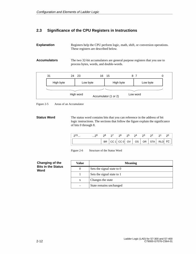
The two 32-bit accumulators are general purpose registers that you use toprocess bytes, words, and double-words.
0781516232431
Accumulator (1 or 2)Low wordHigh word
Low byteHigh byteLow byteHigh byte
Figure 2-5 Areas of an Accumulator
The status word contains bits that you can reference in the address of bitlogic instructions. The sections that follow the figure explain the significanceof bits 0 through 8.
28215... ...29 2427 26 25 2023 22 21
BR OSCC 1 CC 0 OV FCOR STA RLO
Figure 2-6 Structure of the Status Word
Value Meaning
0 Sets the signal state to 0
1 Sets the signal state to 1
x Changes the state
– State remains unchanged
Explanation
Accumulators
Status Word
Changing of theBits in the StatusWord
Configuration and Elements of Ladder Logic
2-13Ladder Logic (LAD) for S7-300 and S7-400C79000-G7076-C564-01
Bit 0 of the status word is called the first-check bit (FC bit, see Figure 2-6).At the start of a ladder logic network, the signal state of the FC bit is always0, unless the previous network ended with –––(SAVE). (The bar over the FCindicates that it is negated, that is, always 0 at the beginning of a ladder logicnetwork.)
Each logic instruction checks the signal state of the FC bit as well as thesignal state of the contact that the instruction addresses. The signal state ofthe FC bit determines the sequence of a logic string. If the FC bit is 0 (at thestart of a ladder logic network), the instruction stores the result in the resultof logic operation bit of the status word and sets the FC bit to 1. Thechecking process is called a first check. The 1 or 0 that is stored in the RLObit after the first check is then referred to as the result of first check.
If the signal state of the FC bit is 1, an operation then links the result of itssignal state check with the RLO formed at the addressed contact since thefirst check, and stores the result in the RLO bit.
A rung of ladder logic instructions (logic string) always ends with an outputinstruction (Set Coil, Reset Coil, or Output Coil) or a jump instruction relatedto the result of logic operation. Such an output instruction resets the FC bitto 0.
Bit 1 of the status word is called the result of logic operation bit (RLO bit,see Figure 2-6). This bit stores the result of a string of bit logic instructions ormath comparisons. The signal state changes of the RLO bit can provideinformation related to power flow.
For example, the first instruction in a network of ladder logic checks thesignal state of a contact and produces a result of 1 or 0. The instruction storesthe result of this signal state check in the RLO bit. The second instruction ina rung of bit logic instructions also checks the signal state of a contact andproduces a result. Then the instruction combines this result with the valuestored in the RLO bit of the status word according to the principles ofBoolean logic (see First Check above and Chapter 4). The result of this logicoperation is stored in the RLO bit of the status word, replacing the formervalue in the RLO bit. Each subsequent instruction in the rung performs alogic operation on two values: the result produced when the instructionchecks the contact, and the current RLO.
You can, for example, use a Boolean bit logic instruction on a first check toassign the state of the contents of a Boolean bit memory location to the RLOor trigger a jump.
First Check
Result of LogicOperation
Configuration and Elements of Ladder Logic
2-14Ladder Logic (LAD) for S7-300 and S7-400
C79000-G7076-C564-01
Bit 2 of the status word is called the status bit (STA bit, see Figure 2-6). Thestatus bit stores the value of a bit that is referenced. The status of a bitinstruction that has read access to the memory (Normally Open Contact,Normally Closed Contact) is always the same as the value of the bit that thisinstruction checks (the bit on which it performs its logic operation). Thestatus of a bit instruction that has write access to the memory (Set Coil, ResetCoil, or Output Coil) is the same as the value of the bit to which theinstruction writes or, if no writing takes place, the same as the value of the bitthat the instruction references. The status bit has no significance for bitinstructions that do not access the memory. Such instructions set the status bitto 1 (STA=1). The status bit is not checked by an instruction. It is interpretedduring program test (program status) only.
Bit 3 of the status word is called the OR bit (see Figure 2-6). The OR bit isneeded if you use Contact instructions to perform logical Or operations withan And function. Logical Or operations correspond to arranging contacts inparallel. The And function corresponds to arranging contacts in series (seeSection 2.2). An And function may contain the following instructions:Normally Open Contact and Normally Closed Contact. The OR bit showsthese instructions that a previously executed And function has supplied thevalue 1 and thus forestalls the result of the logical Or operation. Any otherbit-processing command resets the OR bit.
Bit 5 of the status word is called the overflow bit (OV bit, see Figure 2-6).The OV bit indicates a fault. It is set by a math instruction or a floating-pointcompare instruction after a fault occurs (overflow, illegal operation, illegalnumber). The bit is set or reset in accordance with the result of the math orcomparison operation (fault).
Bit 4 of the status word is called the stored overflow bit (OS bit, seeFigure 2-6). The OS bit is set together with the OV bit if an error occurs.Because the OS bit remains set after the error has been eliminated (unlike theOV bit), it indicates whether or not a error occurred in one of the previouslyexecuted instructions. The following commands reset the OS bit: JOS (jumpafter stored overflow, STL programming), the block call commands, and theblock end commands.
Bits 7 and 6 of the status word are called condition code 1 and conditioncode 0 (CC 1 and CC 0, see Figure 2-6). CC 1 and CC 0 provide informationon the following results or bits:
� Result of a math operation
� Result of a comparison
� Result of a digital operation
� Bits that have been shifted out by a shift or rotate command
Status Bit
OR Bit
Overflow Bit
Stored OverflowBit
Condition Code 1and ConditionCode 0
Configuration and Elements of Ladder Logic
2-15Ladder Logic (LAD) for S7-300 and S7-400C79000-G7076-C564-01
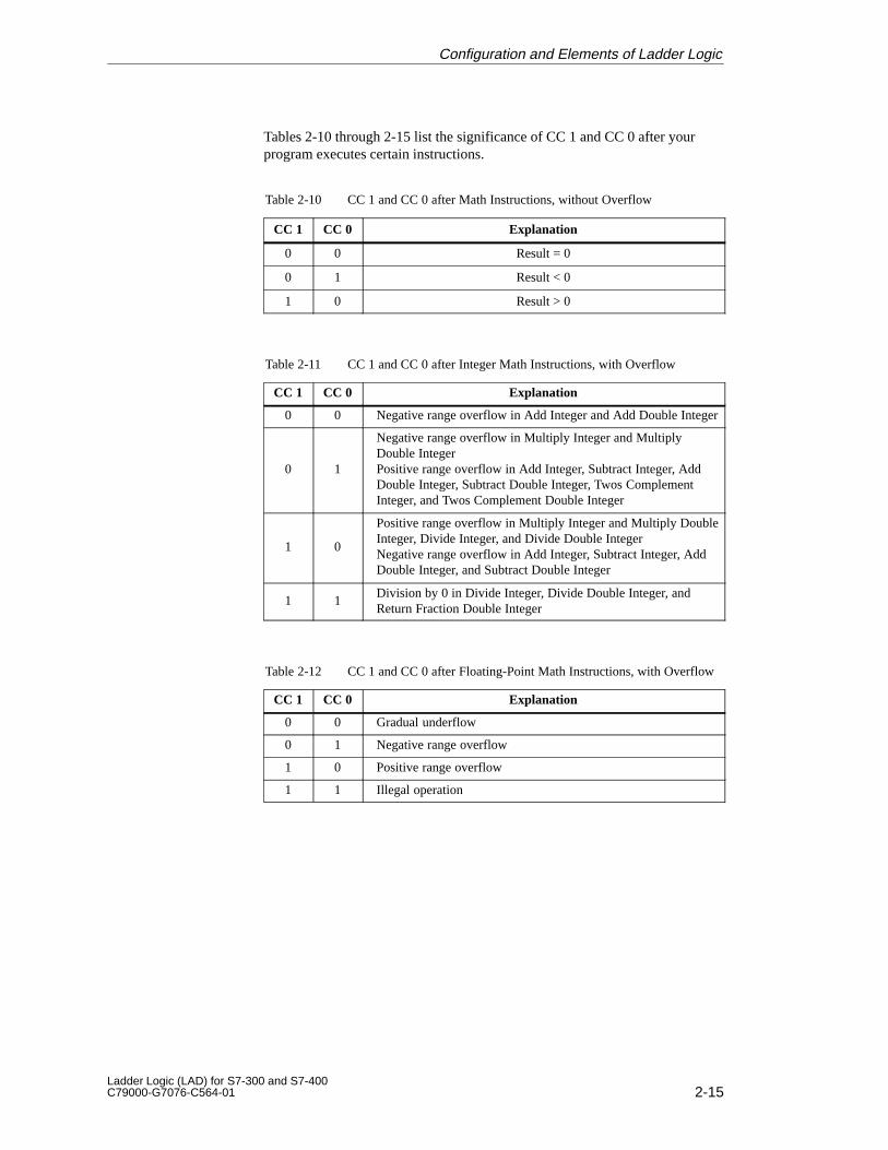
Tables 2-10 through 2-15 list the significance of CC 1 and CC 0 after yourprogram executes certain instructions.
Table 2-10 CC 1 and CC 0 after Math Instructions, without Overflow
CC 1 CC 0 Explanation
0 0 Result = 0
0 1 Result < 0
1 0 Result > 0
Table 2-11 CC 1 and CC 0 after Integer Math Instructions, with Overflow
CC 1 CC 0 Explanation
0 0 Negative range overflow in Add Integer and Add Double Integer
0 1
Negative range overflow in Multiply Integer and MultiplyDouble IntegerPositive range overflow in Add Integer, Subtract Integer, AddDouble Integer, Subtract Double Integer, Twos ComplementInteger, and Twos Complement Double Integer
1 0
Positive range overflow in Multiply Integer and Multiply DoubleInteger, Divide Integer, and Divide Double IntegerNegative range overflow in Add Integer, Subtract Integer, AddDouble Integer, and Subtract Double Integer
1 1Division by 0 in Divide Integer, Divide Double Integer, andReturn Fraction Double Integer
Table 2-12 CC 1 and CC 0 after Floating-Point Math Instructions, with Overflow
CC 1 CC 0 Explanation
0 0 Gradual underflow
0 1 Negative range overflow
1 0 Positive range overflow
1 1 Illegal operation
Configuration and Elements of Ladder Logic
2-16Ladder Logic (LAD) for S7-300 and S7-400
C79000-G7076-C564-01
Table 2-13 CC 1 and CC 0 after Comparison Instructions
CC 1 CC 0 Explanation
0 0 IN2 = IN1
0 1 IN2 < IN1
1 0 IN2 > IN1
1 1 IN1 or IN2 is an illegal floating-point number
Table 2-14 CC 1 and CC 0 after Shift and Rotate Instructions
CC 1 CC 0 Explanation
0 0 Bit shifted out last = 0
1 0 Bit shifted out last = 1
Table 2-15 CC 1 and CC 0 after Word Logic Instructions
CC 1 CC 0 Explanation
0 0 Result = 0
1 0 Result <> 0
Bit 8 of the status word is called the binary result bit (BR bit, see Figure 2-6).The BR bit forms a link between the processing of bits and words. This bitenables your program to interpret the result of a word operation as a binaryresult and to integrate this result in a binary logic chain. Viewed from thisangle, the BR represents a machine-internal memory marker into which theRLO is saved prior to an RLO-changing word operation, so that it is stillavailable for the continuation of the interrupted bit chain after the operationhas been carried out.
For example, the BR bit makes it possible for you to write a function block(FB) or a function (FC) in statement list (STL) and then call the FB or FCfrom ladder logic (LAD).
When writing a function block or function that you want to call from Ladder,no matter whether you write the FB or FC in STL or LAD, you areresponsible for managing the BR bit. The BR bit corresponds to the enableoutput (ENO) of a Ladder box. You should use the SAVE instruction (inSTL) or the or the –––(SAVE) coil (in LAD) to store an RLO in the BR bitaccording to the following criteria:
� Store an RLO of 1 in the BR bit for a case where the FB or FC isexecuted without error.
� Store an RLO of 0 in the BR bit for a case where the FB or FC isexecuted with error
You should program these instructions at the end of the FB or FC so thatthese are the last instructions that are executed in the block.
Binary Result Bit
Configuration and Elements of Ladder Logic
2-17Ladder Logic (LAD) for S7-300 and S7-400C79000-G7076-C564-01
!Warning
Possible unintentional resetting of the BR bit to 0.
When writing FBs and FCs in Ladder, if you fail to manage the BR bit asdescribed above, one FB or FC may overwrite the BR bit of another FBor FC.
To avoid this problem, store the RLO at the end of each FB or FC asdescribed above.
The enable input (EN) and enable output (ENO) parameters of a ladder logicbox function according to the following principles:
� If EN is not activated (that is, if it has a signal state of 0), the box doesnot carry out its function and ENO is not activated (that is, it also has asignal state of 0).
� If EN is activated (that is, if it has a signal state of 1) and the box towhich EN belongs executes its function without error, ENO is alsoactivated (that is, it also has a signal state of 1).
� If EN is activated (that is, if it has a signal state of 1) and an error occurswhile the box to which EN belongs is executing its function, ENO is notactivated (that is, its signal state is 0).
When you call a system function block (SFB) or a system function (SFC) inyour program, the SFB or SFC indicates whether the CPU was able toexecute the function with or without errors by providing the followinginformation in the binary result bit:
� If an error occurred during execution, the BR bit is 0.
� If the function was executed with no error, the BR bit is 1.
Meaning ofEN/ENO
Configuration and Elements of Ladder Logic

2-18Ladder Logic (LAD) for S7-300 and S7-400
C79000-G7076-C564-01
Configuration and Elements of Ladder Logic
3-1Ladder Logic (LAD) for S7-300 and S7-400C79000-G7076-C564-01
Addressing
Section Description Page
3.1 Overview 3-2
3.2 Types of Addresses 3-4
Chapter Overview
3
3-2Ladder Logic (LAD) for S7-300 and S7-400
C79000-G7076-C564-01
3.1 Overview
Many ladder logic instructions work together with one or more addresses(operands). This address indicates a constant or a place where the instructionfinds a variable on which to perform a logic operation. This place can be abit, a byte, a word or a double word of the address.
Possible addresses are, e.g.:
� A constant, the value of a timer or counter, or an ASCII character string
� A bit in the status word of the programmable logic controller
� A data block and a location within the data block area
The following types of addressing are available:
� Immediate addressing (enter a constant as the address)
� Direct addressing (enter a variable as the address)
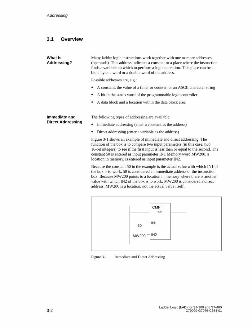
Figure 3-1 shows an example of immediate and direct addressing. Thefunction of the box is to compare two input parameters (in this case, two16-bit integers) to see if the first input is less than or equal to the second. Theconstant 50 is entered as input parameter IN1 Memory word MW200, alocation in memory, is entered as input parameter IN2.
Because the constant 50 in the example is the actual value with which IN1 ofthe box is to work, 50 is considered an immediate address of the instructionbox. Because MW200 points to a location in memory where there is anothervalue with which IN2 of the box is to work, MW200 is considered a directaddress. MW200 is a location, not the actual value itself.
CMP_I <=
IN150
MW200 IN2
Figure 3-1 Immediate and Direct Addressing
What IsAddressing?
Immediate andDirect Addressing
Addressing
3-3Ladder Logic (LAD) for S7-300 and S7-400C79000-G7076-C564-01
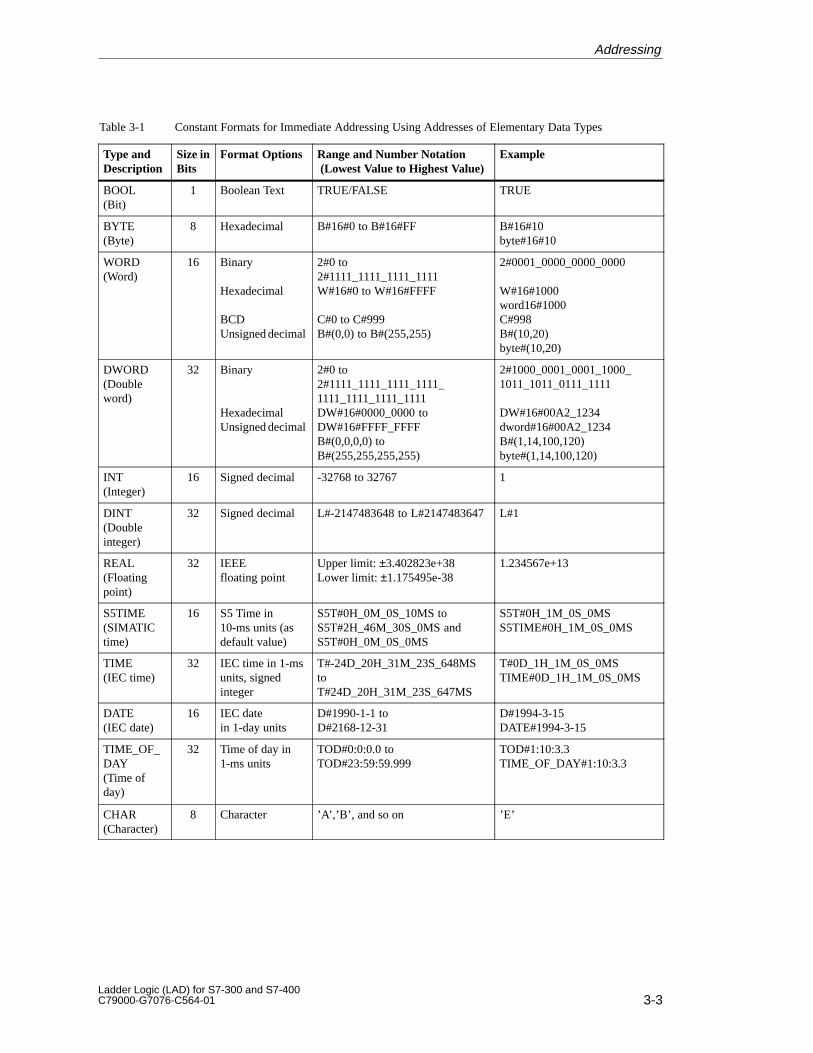
Table 3-1 Constant Formats for Immediate Addressing Using Addresses of Elementary Data Types
Type andDescription
Size inBits
Format Options Range and Number Notation (Lowest Value to Highest Value)
Example
BOOL(Bit)
1 Boolean Text TRUE/FALSE TRUE
BYTE(Byte)
8 Hexadecimal B#16#0 to B#16#FF B#16#10byte#16#10
WORD(Word)
16 Binary
Hexadecimal
BCDUnsigned decimal
2#0 to2#1111_1111_1111_1111W#16#0 to W#16#FFFF
C#0 to C#999B#(0,0) to B#(255,255)
2#0001_0000_0000_0000
W#16#1000word16#1000C#998B#(10,20)byte#(10,20)
DWORD(Doubleword)
32 Binary
HexadecimalUnsigned decimal
2#0 to2#1111_1111_1111_1111_1111_1111_1111_1111DW#16#0000_0000 toDW#16#FFFF_FFFFB#(0,0,0,0) toB#(255,255,255,255)
2#1000_0001_0001_1000_1011_1011_0111_1111
DW#16#00A2_1234dword#16#00A2_1234B#(1,14,100,120)byte#(1,14,100,120)
INT(Integer)
16 Signed decimal -32768 to 32767 1
DINT(Doubleinteger)
32 Signed decimal L#-2147483648 to L#2147483647L#1
REAL(Floatingpoint)
32 IEEEfloating point
Upper limit: ±3.402823e+38Lower limit: ±1.175495e-38
1.234567e+13
S5TIME(SIMATICtime)
16 S5 Time in 10-ms units (asdefault value)
S5T#0H_0M_0S_10MS toS5T#2H_46M_30S_0MS andS5T#0H_0M_0S_0MS
S5T#0H_1M_0S_0MSS5TIME#0H_1M_0S_0MS
TIME(IEC time)
32 IEC time in 1-msunits, signedinteger
T#-24D_20H_31M_23S_648MStoT#24D_20H_31M_23S_647MS
T#0D_1H_1M_0S_0MSTIME#0D_1H_1M_0S_0MS
DATE(IEC date)
16 IEC date in 1-day units
D#1990-1-1 to D#2168-12-31
D#1994-3-15DATE#1994-3-15
TIME_OF_DAY(Time ofday)
32 Time of day in1-ms units
TOD#0:0:0.0 toTOD#23:59:59.999
TOD#1:10:3.3TIME_OF_DAY#1:10:3.3
CHAR(Character)
8 Character ’A’,’B’, and so on ’E’
Addressing
3-4Ladder Logic (LAD) for S7-300 and S7-400
C79000-G7076-C564-01
3.2 Types of Addresses
An address of a ladder logic instruction can indicate any of the followingitems:
� A bit whose signal state is to be checked
� A bit to which the signal state of the logic string is assigned
� A bit to which the result of logic operation (RLO) is assigned
� A bit that is to be set or reset
� A number that indicates a counter that is to be incremented ordecremented
� A number that indicates a timer to be used
� An edge memory bit that stores the previous result of logic operation(RLO)
� An edge memory bit that stores the previous signal state of anotheraddress
� A byte, word, or double word that contains a value with which the ladderelement or box is to work.
� The number of a data block (DB or DI) that is to be opened or created
� The number of a function (FC), system function (SFC), function block(FB), or system function block (SFB) that is to be called
� A label that is to be jumped to
Variables as addresses include an address identifier and a location within thememory area indicated by the address identifier. An address identifier can beone of the following two basic types:
� An address identifier that indicates both of the following:
– The memory area in which an instruction finds a value (data object)on which to perform an operation (for example, I for theprocess-image input area of memory, see Table 2-5)
– The size of the value (data object) on which the instruction is toperform its operation (for example, B for byte, W for word, and D fordouble word, see Table 2-5)
� An address identifier that indicates a memory area but no size of a dataobject in that area (for example, an identifier that indicates the area T fortimer, C for counter, or DB or DI for data block, plus the number of thattimer, counter, or data block, see Table 2-5.
PossibleAddresses
Address Identifiers
Addressing
3-5Ladder Logic (LAD) for S7-300 and S7-400C79000-G7076-C564-01
A pointer is a device that identifies the location of a variable. A pointercontains an address instead of a value. When assigning an actual parameterfor the parameter type “pointer,” you provide the memory address. STEP 7allows you to enter the pointer in either a pointer format or simply as anaddress (such as M 50.0). The following is an example of the pointer formatfor accessing data starting at M 50.0:
P#M50.0
If you are working with an instruction whose address identifier indicates amemory area of your programmable logic controller and a data object that iseither a word or a double word in size, you need to be aware of the fact thatthe memory location is always referenced as a byte location. This bytelocation is the smallest byte number or the number of the high byte. Forexample, the address in the statement shown in Figure 3-2 references foursuccessive bytes in memory area M, starting at byte 10 (MB10) and goingthrough byte 13 (MB13).
Statement: L MD10
Address identifier Byte location
Figure 3-2 Example of Memory Location Referenced as Byte Location
Figure 3-3 illustrates data objects of the following sizes:
� Double word: memory double word MD10
� Word: memory words MW10, MW11, and MW12
� Byte: memory bytes MB10, MB11, MB12, and MB13
When you use absolute addresses that are a word or a double word in width,make sure that you do not create any byte assignments that overlap.
MB10 MB11 MB12 MB13
MW11
MD10
MW10 MW12
Figure 3-3 Referencing a Memory Location as a Byte Location
Pointers
Working with Wordor Double Word asData Object
Addressing

3-6Ladder Logic (LAD) for S7-300 and S7-400
C79000-G7076-C564-01
Addressing
4-1Ladder Logic (LAD) for S7-300 and S7-400C79000-G7076-C564-01
Bit Logic Instructions
Section Description Page
4.1 Overview 4-2
4.2 Normally Open Contact 4-3
4.3 Normally Closed Contact 4-4
4.4 Output Coil 4-5
4.5 Midline Output 4-6
4.6 Invert Power Flow 4-7
4.7 Save RLO to BR Memory 4-8
4.8 Set Coil 4-9
4.9 Reset Coil 4-10
4.10 Set Counter Value 4-11
4.11 Up Counter Coil 4-12
4.12 Down Counter Coil 4-13
4.13 Pulse Timer Coil 4-14
4.14 Extended Pulse Timer Coil 4-15
4.15 On-Delay Timer Coil 4-16
4.16 Retentive On-Delay Timer Coil 4-17
4.17 Off-Delay Timer Coil 4-18
4.18 Positive RLO Edge Detection 4-19
4.19 Negative RLO Edge Detection 4-20
4.20 Address Positive Edge Detection 4-21
4.21 Address Negative Edge Detection 4-22
4.22 Set Reset Flipflop 4-23
4.23 Reset Set Flipflop 4-24
Chapter Overview
4
4-2Ladder Logic (LAD) for S7-300 and S7-400
C79000-G7076-C564-01
4.1 Overview
Bit logic instructions work with two digits, 1 and 0. These two digits formthe base of a number system called the binary system. The two digits 1 and 0are called binary digits or bits. In the world of contacts and coils, a 1indicates activated or energized, and a 0 indicates not activated or notenergized.
The bit logic instructions interpret signal states of 1 and 0 and combine themaccording to Boolean logic. These combinations produce a result of 1 or 0that is called the “result of logic operation” (RLO, see Section 2.3). The logicoperations that are triggered by the bit logic instructions perform a variety offunctions.
There are bit logic instructions to perform the following functions:
� Normally Open Contact and Normally Closed Contact each check thesignal state of a contact and produce a result that is either copied to theresult of logic operation (RLO) bit or is combined with the RLO. If thesecontacts are connected in series, they combine the result of their signalstate check according to the And truth table (see Table 2-8); if they areconnected in parallel, they combine their result according to the Or truthtable (see Table 2-9).
� Output Coil and Midline Output assign the RLO or store it temporarily.
� The following instructions react to an RLO of 1:
– Set Coil and Reset Coil
– Set Reset and Reset Set Flipflops
� Other instructions react to a positive or negative edge transition toperform the following functions:
– Increment or decrement the value of a counter
– Start a timer
– Produce an output of 1
� The remaining instructions affect the RLO directly in the following ways:
– Negate (invert) the RLO
– Save the RLO to the binary result bit of the status word
In this chapter, the counter and timer coils are shown in their internationaland SIMATIC forms.
Explanation
Functions
Bit Logic Instructions
4-3Ladder Logic (LAD) for S7-300 and S7-400C79000-G7076-C564-01
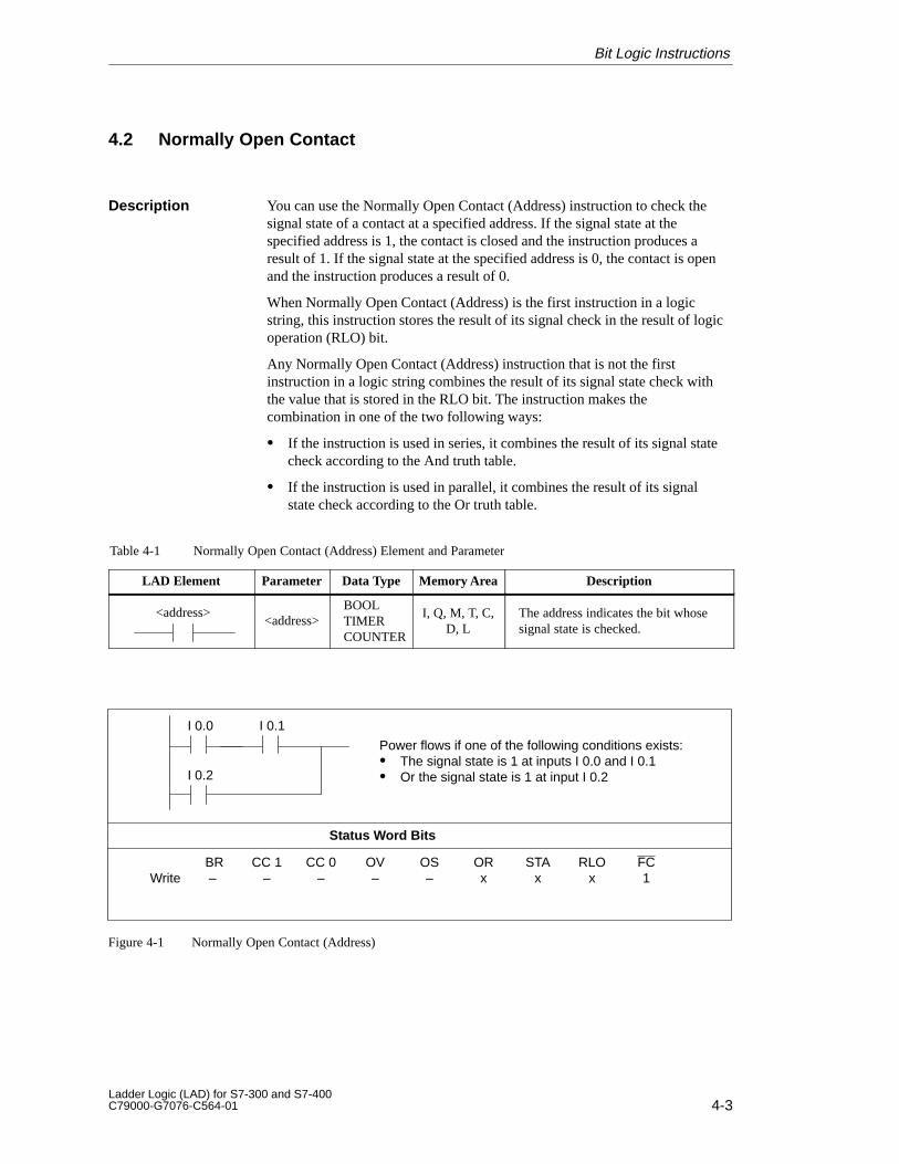
4.2 Normally Open Contact
You can use the Normally Open Contact (Address) instruction to check thesignal state of a contact at a specified address. If the signal state at thespecified address is 1, the contact is closed and the instruction produces aresult of 1. If the signal state at the specified address is 0, the contact is openand the instruction produces a result of 0.
When Normally Open Contact (Address) is the first instruction in a logicstring, this instruction stores the result of its signal check in the result of logicoperation (RLO) bit.
Any Normally Open Contact (Address) instruction that is not the firstinstruction in a logic string combines the result of its signal state check withthe value that is stored in the RLO bit. The instruction makes thecombination in one of the two following ways:
� If the instruction is used in series, it combines the result of its signal statecheck according to the And truth table.
� If the instruction is used in parallel, it combines the result of its signalstate check according to the Or truth table.
Table 4-1 Normally Open Contact (Address) Element and Parameter
LAD Element Parameter Data Type Memory Area Description
<address><address>
BOOLTIMERCOUNTER
I, Q, M, T, C,D, L
The address indicates the bit whosesignal state is checked.
I 0.0
I 0.2
Status Word Bits
I 0.1
Power flows if one of the following conditions exists:� The signal state is 1 at inputs I 0.0 and I 0.1� Or the signal state is 1 at input I 0.2
BR CC 1 CC 0 OV OS OR STA RLO FCWrite – – – – – x x x 1
Figure 4-1 Normally Open Contact (Address)
Description
Bit Logic Instructions
4-4Ladder Logic (LAD) for S7-300 and S7-400
C79000-G7076-C564-01
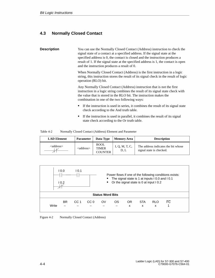
4.3 Normally Closed Contact
You can use the Normally Closed Contact (Address) instruction to check thesignal state of a contact at a specified address. If the signal state at thespecified address is 0, the contact is closed and the instruction produces aresult of 1. If the signal state at the specified address is 1, the contact is openand the instruction produces a result of 0.
When Normally Closed Contact (Address) is the first instruction in a logicstring, this instruction stores the result of its signal check in the result of logicoperation (RLO) bit.
Any Normally Closed Contact (Address) instruction that is not the firstinstruction in a logic string combines the result of its signal state check withthe value that is stored in the RLO bit. The instruction makes thecombination in one of the two following ways:
� If the instruction is used in series, it combines the result of its signal statecheck according to the And truth table.
� If the instruction is used in parallel, it combines the result of its signalstate check according to the Or truth table.
Table 4-2 Normally Closed Contact (Address) Element and Parameter
LAD Element Parameter Data Type Memory Area Description
<address><address>
BOOLTIMERCOUNTER
I, Q, M, T, C,D, L
The address indicates the bit whosesignal state is checked.
I 0.0
I 0.2
Status Word Bits
I 0.1
BR CC 1 CC 0 OV OS OR STA RLO FCWrite – – – – – x x x 1
Power flows if one of the following conditions exists:� The signal state is 1 at inputs I 0.0 and I 0.1� Or the signal state is 0 at input I 0.2
Figure 4-2 Normally Closed Contact (Address)
Description
Bit Logic Instructions
4-5Ladder Logic (LAD) for S7-300 and S7-400C79000-G7076-C564-01
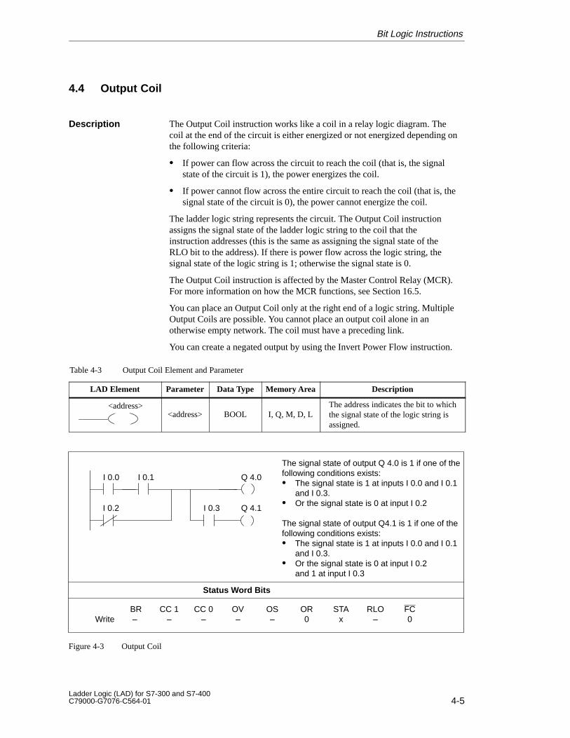
4.4 Output Coil
The Output Coil instruction works like a coil in a relay logic diagram. Thecoil at the end of the circuit is either energized or not energized depending onthe following criteria:
� If power can flow across the circuit to reach the coil (that is, the signalstate of the circuit is 1), the power energizes the coil.
� If power cannot flow across the entire circuit to reach the coil (that is, thesignal state of the circuit is 0), the power cannot energize the coil.
The ladder logic string represents the circuit. The Output Coil instructionassigns the signal state of the ladder logic string to the coil that theinstruction addresses (this is the same as assigning the signal state of theRLO bit to the address). If there is power flow across the logic string, thesignal state of the logic string is 1; otherwise the signal state is 0.
The Output Coil instruction is affected by the Master Control Relay (MCR).For more information on how the MCR functions, see Section 16.5.
You can place an Output Coil only at the right end of a logic string. MultipleOutput Coils are possible. You cannot place an output coil alone in anotherwise empty network. The coil must have a preceding link.
You can create a negated output by using the Invert Power Flow instruction.
Table 4-3 Output Coil Element and Parameter
LAD Element Parameter Data Type Memory Area Description
<address><address> BOOL I, Q, M, D, L
The address indicates the bit to whichthe signal state of the logic string isassigned.
I 0.0
I 0.2
Status Word Bits
I 0.1
The signal state of output Q 4.0 is 1 if one of thefollowing conditions exists:� The signal state is 1 at inputs I 0.0 and I 0.1
and I 0.3.� Or the signal state is 0 at input I 0.2
The signal state of output Q4.1 is 1 if one of thefollowing conditions exists:� The signal state is 1 at inputs I 0.0 and I 0.1
and I 0.3.� Or the signal state is 0 at input I 0.2
and 1 at input I 0.3
BR CC 1 CC 0 OV OS OR STA RLO FCWrite – – – – – 0 x – 0
I 0.3
Q 4.0
Q 4.1
Figure 4-3 Output Coil
Description
Bit Logic Instructions
4-6Ladder Logic (LAD) for S7-300 and S7-400
C79000-G7076-C564-01
4.5 Midline Output
The Midline Output instruction is an intermediate assigning element thatstores the RLO. This intermediate assigning element saves the bit logiccombination of the last open branch until the assigning element is reached. Ina series with other contacts, the Midline Output functions as a normalcontact.
The Midline Output instruction is affected by the Master Control Relay(MCR). For more information on how the MCR functions, see Section 16.5.
Certain restrictions apply to the placement of a Midline Output. For example,a Midline Output element can never be located at the end of a network or atthe end of an open branch. See also Section 2.1.
You can create a negated output by using the Invert Power Flow instruction.
Table 4-4 Midline Output Element and Parameter
LAD Element Parameter Data Type Memory Area Description
#<address>
<address> BOOL I, Q, M, D, L1 The address indicates the bit to whichthe RLO is assigned.
1 For the Midline Output instruction, you can only use an address in the L memory area if you declare it in VAR_TEMP.You cannot use the L memory area for an absolute address with this instruction.
The following Midline Outputs have the following RLOs:
M 0.0 has the RLO of
M 1.1 has the RLO of
M 2.2 has the RLO of the complete bit logic combination.
I 1.0
Status Word Bits
I 1.1
BR CC 1 CC 0 OV OS OR STA RLO FCWrite – – – – – 0 x – 1
M 0.0
#
I 1.2 I 1.3
NOT
M 1.1
# NOT
M 2.2
#
Q 4.0
I 1.0 I 1.1
I 1.2 I 1.3
NOT
I 1.0 I 1.1 M 0.0
#
Figure 4-4 Midline Output
Description
Bit Logic Instructions
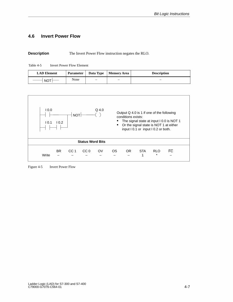
4-7Ladder Logic (LAD) for S7-300 and S7-400C79000-G7076-C564-01
4.6 Invert Power Flow
The Invert Power Flow instruction negates the RLO.
Table 4-5 Invert Power Flow Element
LAD Element Parameter Data Type Memory Area Description
NOT None – – –
Status Word Bits
BR CC 1 CC 0 OV OS OR STA RLO FCWrite – – – – – – 1 * –
I 0.0
I 0.1 I 0.2
Q 4.0Output Q 4.0 is 1 if one of the followingconditions exists:� The signal state at input I 0.0 is NOT 1� Or the signal state is NOT 1 at either
input I 0.1 or input I 0.2 or both.
NOT
Figure 4-5 Invert Power Flow
Description
Bit Logic Instructions
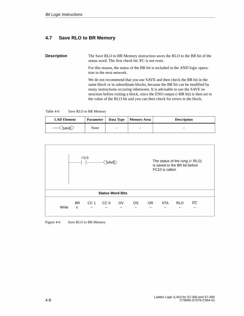
4-8Ladder Logic (LAD) for S7-300 and S7-400
C79000-G7076-C564-01
4.7 Save RLO to BR Memory
The Save RLO to BR Memory instruction saves the RLO to the BR bit of thestatus word. The first check bit /FC is not reset.
For this reason, the status of the BR bit is included in the AND logic opera-tion in the next network.
We do not recommend that you use SAVE and then check the BR bit in thesame block or in subordinate blocks, because the BR bit can be modified bymany instructions occuring inbetween. It is advisable to use the SAVE in-struction before exiting a block, since the ENO output (=BR bit) is then set tothe value of the RLO bit and you can then check for errors in the block.
Table 4-6 Save RLO to BR Memory
LAD Element Parameter Data Type Memory Area Description
SAVE None – – –
Status Word Bits
BR CC 1 CC 0 OV OS OR STA RLO FCWrite x – – – – – – – –
The status of the rung (= RLO)is saved to the BR bit beforeFC10 is called.
SAVEI 0.0
Figure 4-6 Save RLO to BR Memory
Description
Bit Logic Instructions
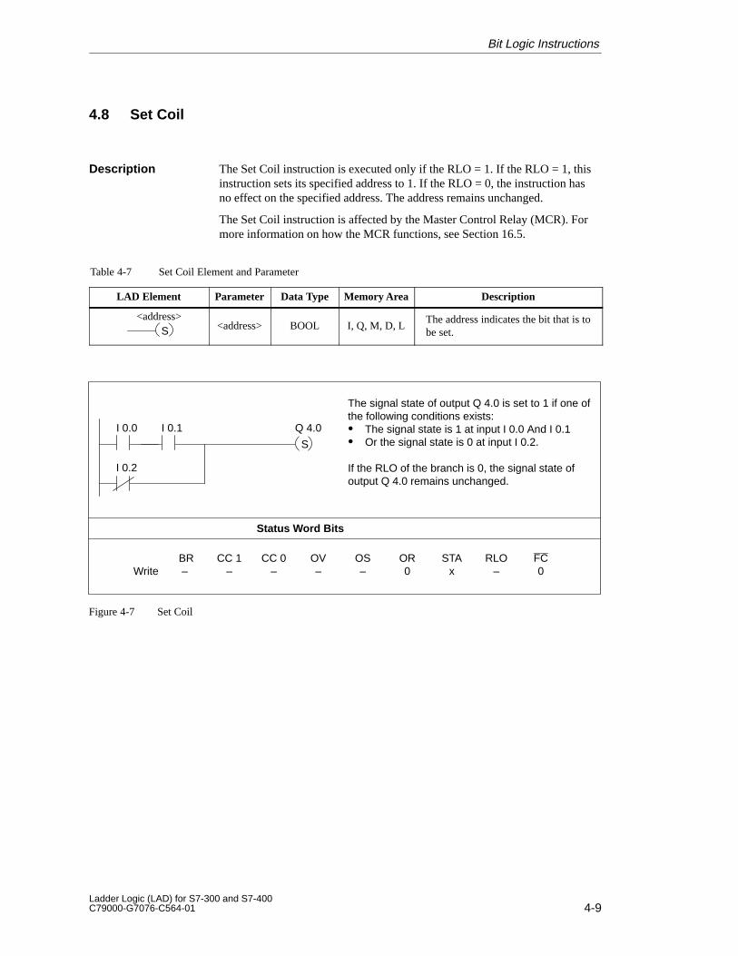
4-9Ladder Logic (LAD) for S7-300 and S7-400C79000-G7076-C564-01
4.8 Set Coil
The Set Coil instruction is executed only if the RLO = 1. If the RLO = 1, thisinstruction sets its specified address to 1. If the RLO = 0, the instruction hasno effect on the specified address. The address remains unchanged.
The Set Coil instruction is affected by the Master Control Relay (MCR). Formore information on how the MCR functions, see Section 16.5.
Table 4-7 Set Coil Element and Parameter
LAD Element Parameter Data Type Memory Area Description
S<address>
<address> BOOL I, Q, M, D, LThe address indicates the bit that is tobe set.
Status Word Bits
BR CC 1 CC 0 OV OS OR STA RLO FCWrite – – – – – 0 x – 0
I 0.0
I 0.2
I 0.1 Q 4.0
S
The signal state of output Q 4.0 is set to 1 if one ofthe following conditions exists:� The signal state is 1 at input I 0.0 And I 0.1� Or the signal state is 0 at input I 0.2.
If the RLO of the branch is 0, the signal state ofoutput Q 4.0 remains unchanged.
Figure 4-7 Set Coil
Description
Bit Logic Instructions
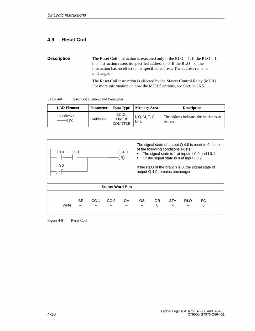
4-10Ladder Logic (LAD) for S7-300 and S7-400
C79000-G7076-C564-01
4.9 Reset Coil
The Reset Coil instruction is executed only if the RLO = 1. If the RLO = 1,this instruction resets its specified address to 0. If the RLO = 0, theinstruction has no effect on its specified address. The address remainsunchanged.
The Reset Coil instruction is affected by the Master Control Relay (MCR).For more information on how the MCR functions, see Section 16.5.
Table 4-8 Reset Coil Element and Parameter
LAD Element Parameter Data Type Memory Area Description
R<address>
<address>BOOLTIMER
COUNTER
I, Q, M, T, C,D, L
The address indicates the bit that is tobe reset.
Status Word Bits
BR CC 1 CC 0 OV OS OR STA RLO FCWrite – – – – – 0 x – 0
I 0.0
I 0.2
I 0.1 Q 4.0
R
The signal state of output Q 4.0 is reset to 0 if oneof the following conditions exists:� The signal state is 1 at inputs I 0.0 and I 0.1� Or the signal state is 0 at input I 0.2
If the RLO of the branch is 0, the signal state ofoutput Q 4.0 remains unchanged.
Figure 4-8 Reset Coil
Description
Bit Logic Instructions
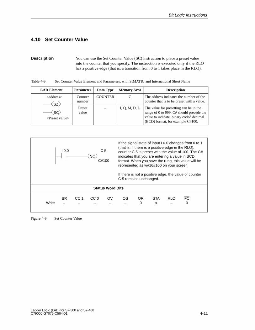
4-11Ladder Logic (LAD) for S7-300 and S7-400C79000-G7076-C564-01
4.10 Set Counter Value
You can use the Set Counter Value (SC) instruction to place a preset valueinto the counter that you specify. The instruction is executed only if the RLOhas a positive edge (that is, a transition from 0 to 1 takes place in the RLO).
Table 4-9 Set Counter Value Element and Parameters, with SIMATIC and International Short Name
LAD Element Parameter Data Type Memory Area Description
SZ
<address> Counternumber
COUNTER C The address indicates the number of thecounter that is to be preset with a value.
SZ
SC
<Preset value>
Presetvalue
– I, Q, M, D, L The value for presetting can be in therange of 0 to 999. C# should precede thevalue to indicate binary coded decimal(BCD) format, for example C#100.
Status Word Bits
BR CC 1 CC 0 OV OS OR STA RLO FCWrite – – – – – 0 x – 0
I 0.0 C 5
SC
If the signal state of input I 0.0 changes from 0 to 1(that is, if there is a positive edge in the RLO),counter C 5 is preset with the value of 100. The C#indicates that you are entering a value in BCDformat. When you save the rung, this value will berepresented as w#16#100 on your screen.
If there is not a positive edge, the value of counterC 5 remains unchanged.
C#100
Figure 4-9 Set Counter Value
Description
Bit Logic Instructions
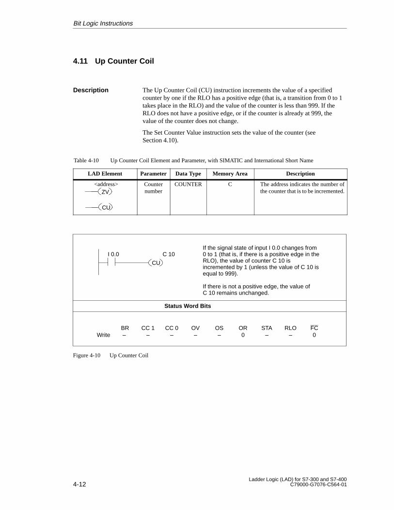
4-12Ladder Logic (LAD) for S7-300 and S7-400
C79000-G7076-C564-01
4.11 Up Counter Coil
The Up Counter Coil (CU) instruction increments the value of a specifiedcounter by one if the RLO has a positive edge (that is, a transition from 0 to 1takes place in the RLO) and the value of the counter is less than 999. If theRLO does not have a positive edge, or if the counter is already at 999, thevalue of the counter does not change.
The Set Counter Value instruction sets the value of the counter (seeSection 4.10).
Table 4-10 Up Counter Coil Element and Parameter, with SIMATIC and International Short Name
LAD Element Parameter Data Type Memory Area Description
ZV<address>
CU
Counternumber
COUNTER C The address indicates the number ofthe counter that is to be incremented.
Status Word Bits
BR CC 1 CC 0 OV OS OR STA RLO FCWrite – – – – – 0 – – 0
I 0.0 C 10
CU
If the signal state of input I 0.0 changes from0 to 1 (that is, if there is a positive edge in theRLO), the value of counter C 10 isincremented by 1 (unless the value of C 10 isequal to 999).
If there is not a positive edge, the value ofC 10 remains unchanged.
Figure 4-10 Up Counter Coil
Description
Bit Logic Instructions
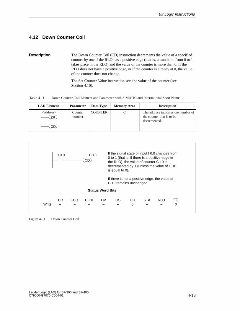
4-13Ladder Logic (LAD) for S7-300 and S7-400C79000-G7076-C564-01
4.12 Down Counter Coil
The Down Counter Coil (CD) instruction decrements the value of a specifiedcounter by one if the RLO has a positive edge (that is, a transition from 0 to 1takes place in the RLO) and the value of the counter is more than 0. If theRLO does not have a positive edge, or if the counter is already at 0, the valueof the counter does not change.
The Set Counter Value instruction sets the value of the counter (seeSection 4.10).
Table 4-11 Down Counter Coil Element and Parameter, with SIMATIC and International Short Name
LAD Element Parameter Data Type Memory Area Description
<address>
ZR
CD
Counternumber
COUNTER C The address indicates the number ofthe counter that is to bedecremented.
Status Word Bits
BR CC 1 CC 0 OV OS OR STA RLO FCWrite – – – – – 0 – – 0
I 0.0 C 10
CD
If the signal state of input I 0.0 changes from0 to 1 (that is, if there is a positive edge inthe RLO), the value of counter C 10 isdecremented by 1 (unless the value of C 10is equal to 0).
If there is not a positive edge, the value ofC 10 remains unchanged.
Figure 4-11 Down Counter Coil
Description
Bit Logic Instructions
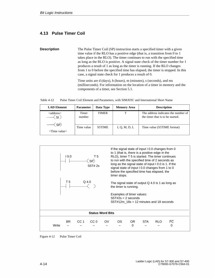
4-14Ladder Logic (LAD) for S7-300 and S7-400
C79000-G7076-C564-01
4.13 Pulse Timer Coil
The Pulse Timer Coil (SP) instruction starts a specified timer with a giventime value if the RLO has a positive edge (that is, a transition from 0 to 1takes place in the RLO). The timer continues to run with the specified timeas long as the RLO is positive. A signal state check of the timer number for 1produces a result of 1 as long as the timer is running. If the RLO changesfrom 1 to 0 before the specified time has elapsed, the timer is stopped. In thiscase, a signal state check for 1 produces a result of 0.
Time units are d (days), h (hours), m (minutes), s (seconds), and ms(milliseconds). For information on the location of a timer in memory and thecomponents of a timer, see Section 5.1.
Table 4-12 Pulse Timer Coil Element and Parameters, with SIMATIC and International Short Name
LAD Element Parameter Data Type Memory Area Description
SI<address>
SP
Timernumber
TIMER T The address indicates the number ofthe timer that is to be started.
<Time value>
SPTime value S5TIME I, Q, M, D, L Time value (S5TIME format)
SP
Status Word Bits
BR CC 1 CC 0 OV OS OR STA RLO FCWrite – – – – – 0 – – 0
I 0.0 T 5
If the signal state of input I 0.0 changes from 0to 1 (that is, there is a positive edge in theRLO), timer T 5 is started. The timer continuesto run with the specified time of 2 seconds aslong as the signal state of input I 0.0 is 1. If thesignal state of input I 0.0 changes from 1 to 0before the specified time has elapsed, thetimer stops.
The signal state of output Q 4.0 is 1 as long asthe timer is running.
Examples of timer values:S5T#2s = 2 secondsS5T#12m_18s = 12 minutes and 18 seconds
T 5 Q 4.0
S5T# 2s
Figure 4-12 Pulse Timer Coil
Description
Bit Logic Instructions
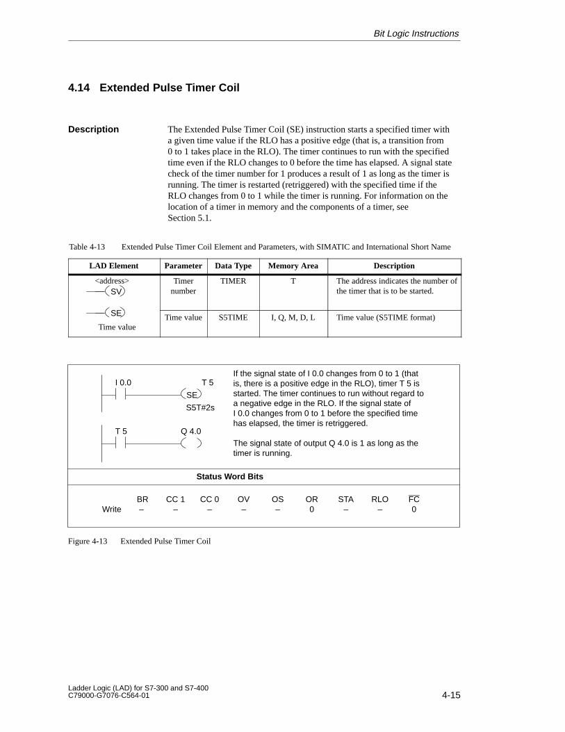
4-15Ladder Logic (LAD) for S7-300 and S7-400C79000-G7076-C564-01
4.14 Extended Pulse Timer Coil
The Extended Pulse Timer Coil (SE) instruction starts a specified timer witha given time value if the RLO has a positive edge (that is, a transition from0 to 1 takes place in the RLO). The timer continues to run with the specifiedtime even if the RLO changes to 0 before the time has elapsed. A signal statecheck of the timer number for 1 produces a result of 1 as long as the timer isrunning. The timer is restarted (retriggered) with the specified time if theRLO changes from 0 to 1 while the timer is running. For information on thelocation of a timer in memory and the components of a timer, seeSection 5.1.
Table 4-13 Extended Pulse Timer Coil Element and Parameters, with SIMATIC and International Short Name
LAD Element Parameter Data Type Memory Area Description
SV<address>
SE
Timernumber
TIMER T The address indicates the number ofthe timer that is to be started.
Time value
SE Time value S5TIME I, Q, M, D, L Time value (S5TIME format)
SE
Status Word Bits
BR CC 1 CC 0 OV OS OR STA RLO FCWrite – – – – – 0 – – 0
I 0.0 T 5If the signal state of I 0.0 changes from 0 to 1 (thatis, there is a positive edge in the RLO), timer T 5 isstarted. The timer continues to run without regard toa negative edge in the RLO. If the signal state ofI 0.0 changes from 0 to 1 before the specified timehas elapsed, the timer is retriggered.
The signal state of output Q 4.0 is 1 as long as thetimer is running.
T 5 Q 4.0
S5T#2s
Figure 4-13 Extended Pulse Timer Coil
Description
Bit Logic Instructions
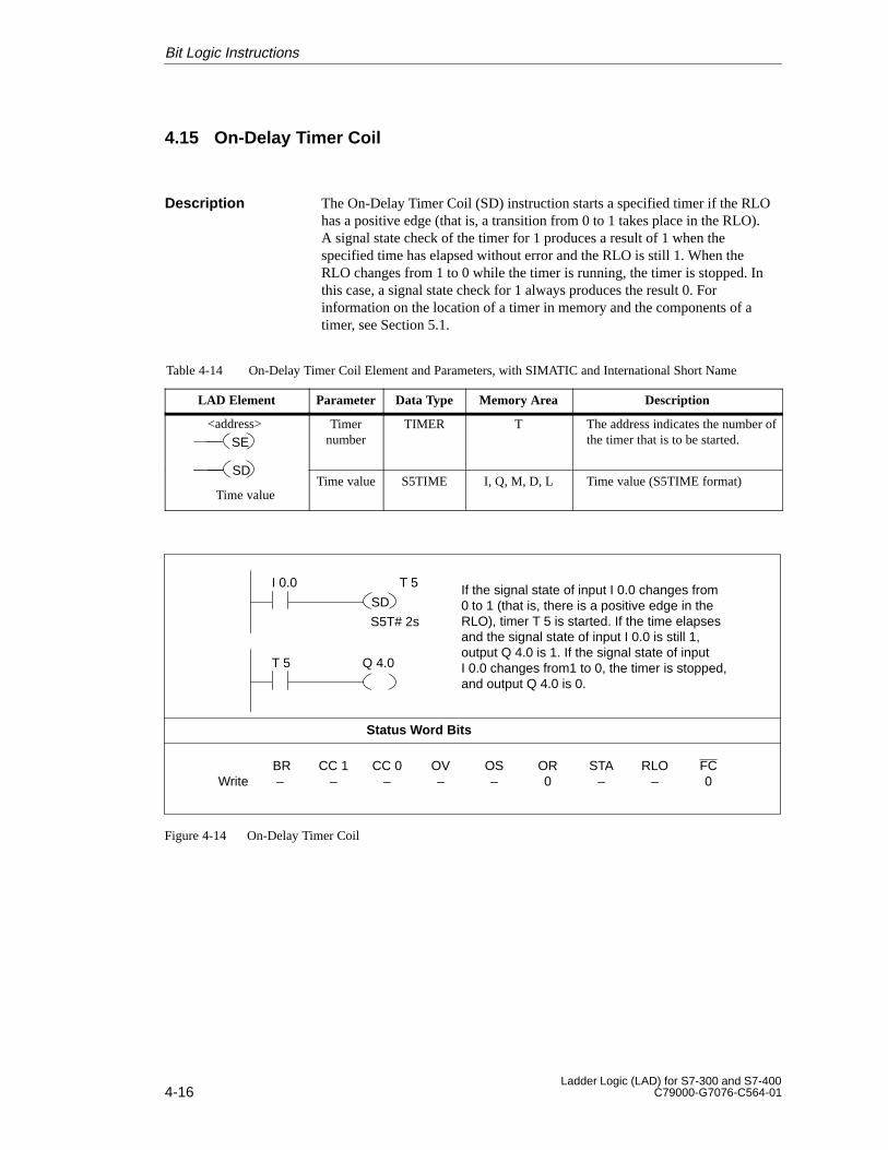
4-16Ladder Logic (LAD) for S7-300 and S7-400
C79000-G7076-C564-01
4.15 On-Delay Timer Coil
The On-Delay Timer Coil (SD) instruction starts a specified timer if the RLOhas a positive edge (that is, a transition from 0 to 1 takes place in the RLO).A signal state check of the timer for 1 produces a result of 1 when thespecified time has elapsed without error and the RLO is still 1. When theRLO changes from 1 to 0 while the timer is running, the timer is stopped. Inthis case, a signal state check for 1 always produces the result 0. Forinformation on the location of a timer in memory and the components of atimer, see Section 5.1.
Table 4-14 On-Delay Timer Coil Element and Parameters, with SIMATIC and International Short Name
LAD Element Parameter Data Type Memory Area Description
SE<address>
SD
Timernumber
TIMER T The address indicates the number ofthe timer that is to be started.
Time value
SDTime value S5TIME I, Q, M, D, L Time value (S5TIME format)
Status Word Bits
BR CC 1 CC 0 OV OS OR STA RLO FCWrite – – – – – 0 – – 0
I 0.0 T 5
SDIf the signal state of input I 0.0 changes from0 to 1 (that is, there is a positive edge in theRLO), timer T 5 is started. If the time elapsesand the signal state of input I 0.0 is still 1,output Q 4.0 is 1. If the signal state of input I 0.0 changes from1 to 0, the timer is stopped,and output Q 4.0 is 0.
T 5 Q 4.0
S5T# 2s
Figure 4-14 On-Delay Timer Coil
Description
Bit Logic Instructions
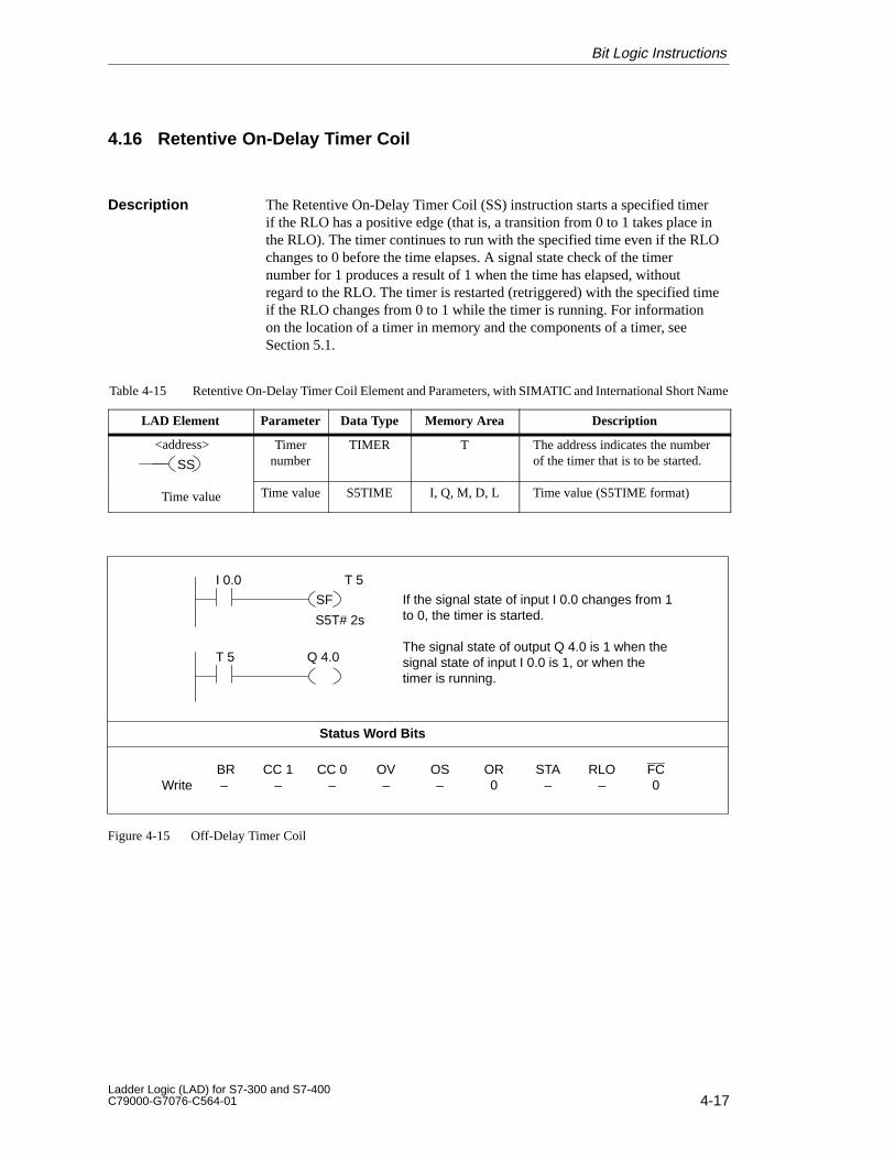
4-17Ladder Logic (LAD) for S7-300 and S7-400C79000-G7076-C564-01
4.16 Retentive On-Delay Timer Coil
The Retentive On-Delay Timer Coil (SS) instruction starts a specified timerif the RLO has a positive edge (that is, a transition from 0 to 1 takes place inthe RLO). The timer continues to run with the specified time even if the RLOchanges to 0 before the time elapses. A signal state check of the timernumber for 1 produces a result of 1 when the time has elapsed, withoutregard to the RLO. The timer is restarted (retriggered) with the specified timeif the RLO changes from 0 to 1 while the timer is running. For informationon the location of a timer in memory and the components of a timer, seeSection 5.1.
Table 4-15 Retentive On-Delay Timer Coil Element and Parameters, with SIMATIC and International Short Name
LAD Element Parameter Data Type Memory Area Description
SS
<address> Timernumber
TIMER T The address indicates the number of the timer that is to be started.
Time value Time value S5TIME I, Q, M, D, L Time value (S5TIME format)
Status Word Bits
BR CC 1 CC 0 OV OS OR STA RLO FCWrite – – – – – 0 – – 0
I 0.0 T 5
SF If the signal state of input I 0.0 changes from 1to 0, the timer is started.
The signal state of output Q 4.0 is 1 when thesignal state of input I 0.0 is 1, or when thetimer is running.
T 5 Q 4.0
S5T# 2s
Figure 4-15 Off-Delay Timer Coil
Description
Bit Logic Instructions
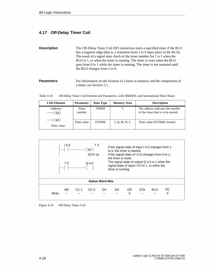
4-18Ladder Logic (LAD) for S7-300 and S7-400
C79000-G7076-C564-01
4.17 Off-Delay Timer Coil
The Off-Delay Timer Coil (SF) instruction starts a specified timer if the RLOhas a negative edge (that is, a transition from 1 to 0 takes place in the RLO).The result of a signal state check of the timer number for 1 is 1 when theRLO is 1, or when the timer is running. The timer is reset when the RLOgoes from 0 to 1 while the timer is running. The timer is not restarted untilthe RLO changes from 1 to 0.
For information on the location of a timer in memory and the components ofa timer, see Section 5.1.
Table 4-16 Off-Delay Timer Coil Element and Parameters, with SIMATIC and International Short Name
LAD Element Parameter Data Type Memory Area Description
SA<address>
SF
Timernumber
TIMER T The address indicates the number of the timer that is to be started.
Time value
SFTime value S5TIME I, Q, M, D, L Time value (S5TIME format)
Status Word Bits
BR CC 1 CC 0 OV OS OR STA RLO FCWrite – – – – – 0 – – 0
I 0.0 T 5
SFIf the signal state of input I 0.0 changes from 1to 0, the timer is started. If the signal state of I 0.0 changes from 0 to 1,the timer is reset. The signal state of output Q 4.0 is 1 when thesignal state of input I 0.0 is 1, or when thetimer is running.
T 5 Q 4.0
S5T# 2s
Figure 4-16 Off-Delay Timer Coil
Description
Parameters
Bit Logic Instructions
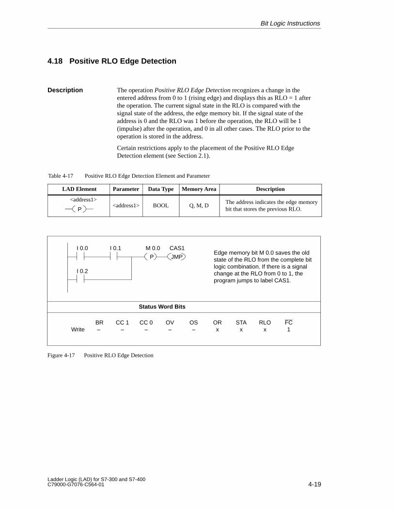
4-19Ladder Logic (LAD) for S7-300 and S7-400C79000-G7076-C564-01
4.18 Positive RLO Edge Detection
The operation Positive RLO Edge Detection recognizes a change in theentered address from 0 to 1 (rising edge) and displays this as RLO = 1 afterthe operation. The current signal state in the RLO is compared with thesignal state of the address, the edge memory bit. If the signal state of theaddress is 0 and the RLO was 1 before the operation, the RLO will be 1(impulse) after the operation, and 0 in all other cases. The RLO prior to theoperation is stored in the address.
Certain restrictions apply to the placement of the Positive RLO EdgeDetection element (see Section 2.1).
Table 4-17 Positive RLO Edge Detection Element and Parameter
LAD Element Parameter Data Type Memory Area Description
P
<address1><address1> BOOL Q, M, D
The address indicates the edge memorybit that stores the previous RLO.
Status Word Bits
BR CC 1 CC 0 OV OS OR STA RLO FCWrite – – – – – x x x 1
I 0.0 CAS1Edge memory bit M 0.0 saves the oldstate of the RLO from the complete bitlogic combination. If there is a signalchange at the RLO from 0 to 1, theprogram jumps to label CAS1.
I 0.2
I 0.1
P JMP
M 0.0
Figure 4-17 Positive RLO Edge Detection
Description
Bit Logic Instructions
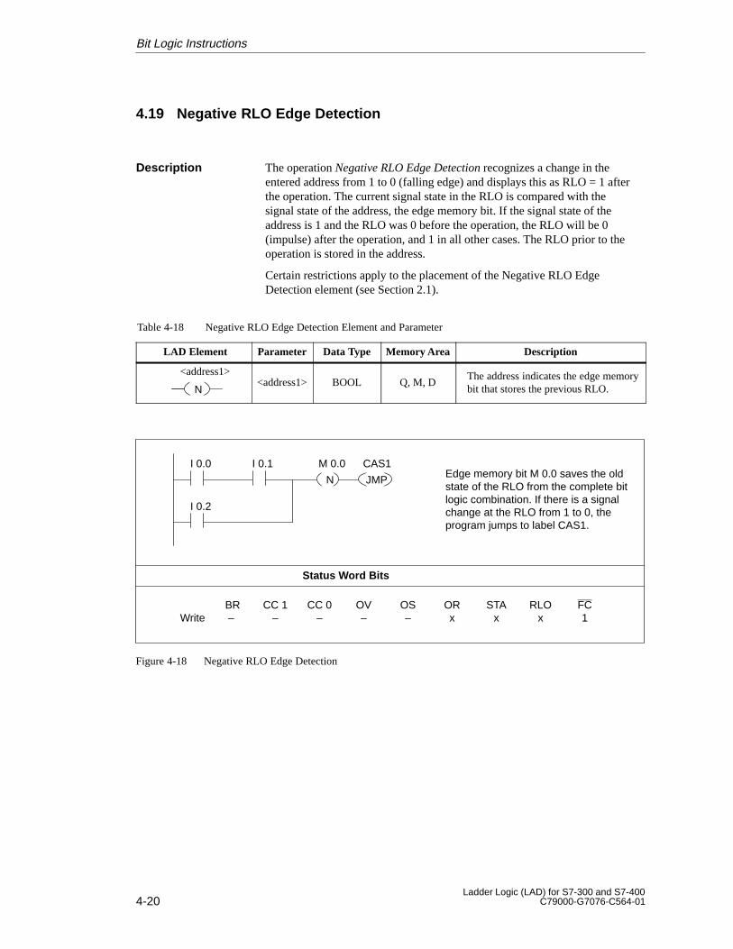
4-20Ladder Logic (LAD) for S7-300 and S7-400
C79000-G7076-C564-01
4.19 Negative RLO Edge Detection
The operation Negative RLO Edge Detection recognizes a change in theentered address from 1 to 0 (falling edge) and displays this as RLO = 1 afterthe operation. The current signal state in the RLO is compared with thesignal state of the address, the edge memory bit. If the signal state of theaddress is 1 and the RLO was 0 before the operation, the RLO will be 0(impulse) after the operation, and 1 in all other cases. The RLO prior to theoperation is stored in the address.
Certain restrictions apply to the placement of the Negative RLO EdgeDetection element (see Section 2.1).
Table 4-18 Negative RLO Edge Detection Element and Parameter
LAD Element Parameter Data Type Memory Area Description
N
<address1><address1> BOOL Q, M, D
The address indicates the edge memorybit that stores the previous RLO.
Status Word Bits
BR CC 1 CC 0 OV OS OR STA RLO FCWrite – – – – – x x x 1
I 0.0 CAS1Edge memory bit M 0.0 saves the oldstate of the RLO from the complete bitlogic combination. If there is a signalchange at the RLO from 1 to 0, theprogram jumps to label CAS1.
I 0.2
I 0.1
N JMP
M 0.0
Figure 4-18 Negative RLO Edge Detection
Description
Bit Logic Instructions
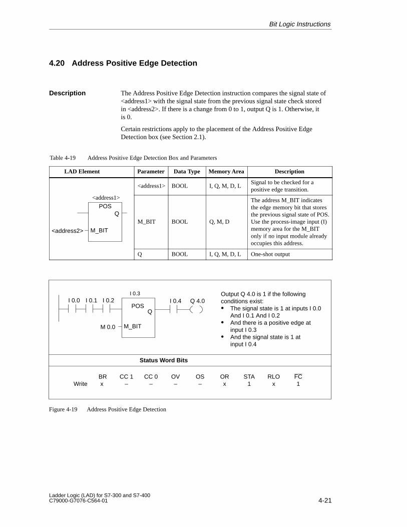
4-21Ladder Logic (LAD) for S7-300 and S7-400C79000-G7076-C564-01
4.20 Address Positive Edge Detection
The Address Positive Edge Detection instruction compares the signal state of<address1> with the signal state from the previous signal state check storedin <address2>. If there is a change from 0 to 1, output Q is 1. Otherwise, itis 0.
Certain restrictions apply to the placement of the Address Positive EdgeDetection box (see Section 2.1).
Table 4-19 Address Positive Edge Detection Box and Parameters
LAD Element Parameter Data Type Memory Area Description
dd 1
<address1> BOOL I, Q, M, D, LSignal to be checked for apositive edge transition.
POS
M_BIT
Q
<address1>
<address2>
M_BIT BOOL Q, M, D
The address M_BIT indicatesthe edge memory bit that storesthe previous signal state of POS.Use the process-image input (I)memory area for the M_BITonly if no input module alreadyoccupies this address.
Q BOOL I, Q, M, D, L One-shot output
Status Word Bits
BR CC 1 CC 0 OV OS OR STA RLO FCWrite x – – – – x 1 x 1
I 0.0Output Q 4.0 is 1 if the followingconditions exist:� The signal state is 1 at inputs I 0.0
And I 0.1 And I 0.2� And there is a positive edge at
input I 0.3� And the signal state is 1 at
input I 0.4
I 0.2I 0.1 I 0.3
POS
M_BIT
Q
M 0.0
Q 4.0I 0.4
Figure 4-19 Address Positive Edge Detection
Description
Bit Logic Instructions
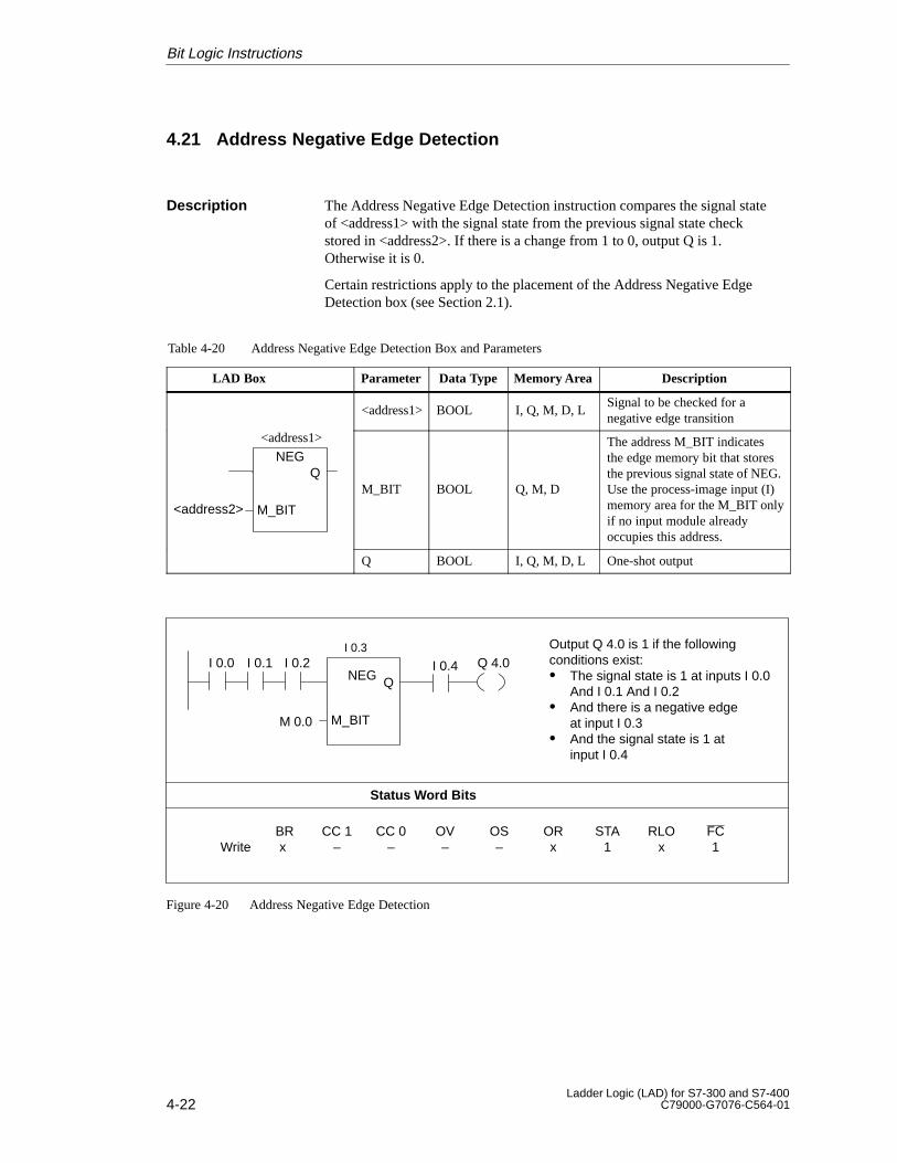
4-22Ladder Logic (LAD) for S7-300 and S7-400
C79000-G7076-C564-01
4.21 Address Negative Edge Detection
The Address Negative Edge Detection instruction compares the signal stateof <address1> with the signal state from the previous signal state checkstored in <address2>. If there is a change from 1 to 0, output Q is 1.Otherwise it is 0.
Certain restrictions apply to the placement of the Address Negative EdgeDetection box (see Section 2.1).
Table 4-20 Address Negative Edge Detection Box and Parameters
LAD Box Parameter Data Type Memory Area Description
<address1> BOOL I, Q, M, D, LSignal to be checked for anegative edge transition
NEG
M_BIT
Q
<address2>
<address1>
M_BIT BOOL Q, M, D
The address M_BIT indicates the edge memory bit that storesthe previous signal state of NEG. Use the process-image input (I)memory area for the M_BIT onlyif no input module alreadyoccupies this address.
Q BOOL I, Q, M, D, L One-shot output
Status Word Bits
BR CC 1 CC 0 OV OS OR STA RLO FCWrite x – – – – x 1 x 1
I 0.0 I 0.2I 0.1 I 0.3
NEG
M_BIT
Q
M 0.0
Q 4.0I 0.4
Output Q 4.0 is 1 if the followingconditions exist:� The signal state is 1 at inputs I 0.0
And I 0.1 And I 0.2� And there is a negative edge
at input I 0.3� And the signal state is 1 at
input I 0.4
Figure 4-20 Address Negative Edge Detection
Description
Bit Logic Instructions
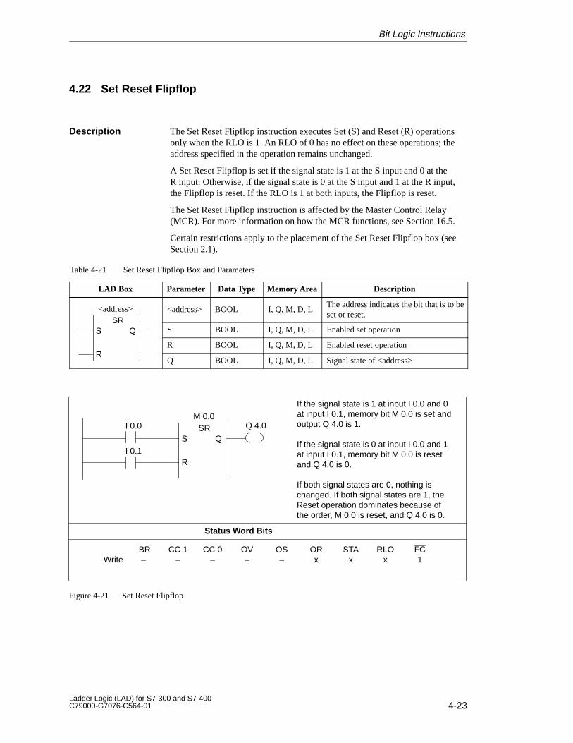
4-23Ladder Logic (LAD) for S7-300 and S7-400C79000-G7076-C564-01
4.22 Set Reset Flipflop
The Set Reset Flipflop instruction executes Set (S) and Reset (R) operationsonly when the RLO is 1. An RLO of 0 has no effect on these operations; theaddress specified in the operation remains unchanged.
A Set Reset Flipflop is set if the signal state is 1 at the S input and 0 at theR input. Otherwise, if the signal state is 0 at the S input and 1 at the R input,the Flipflop is reset. If the RLO is 1 at both inputs, the Flipflop is reset.
The Set Reset Flipflop instruction is affected by the Master Control Relay(MCR). For more information on how the MCR functions, see Section 16.5.
Certain restrictions apply to the placement of the Set Reset Flipflop box (seeSection 2.1).
Table 4-21 Set Reset Flipflop Box and Parameters
LAD Box Parameter Data Type Memory Area Description
SR<address> <address> BOOL I, Q, M, D, L
The address indicates the bit that is to beset or reset.
SRQS S BOOL I, Q, M, D, L Enabled set operation
RR BOOL I, Q, M, D, L Enabled reset operation
RQ BOOL I, Q, M, D, L Signal state of <address>
Status Word Bits
BR CC 1 CC 0 OV OS OR STA RLO FCWrite – – – – – x x x 1
I 0.0
If the signal state is 1 at input I 0.0 and 0at input I 0.1, memory bit M 0.0 is set andoutput Q 4.0 is 1.
If the signal state is 0 at input I 0.0 and 1at input I 0.1, memory bit M 0.0 is resetand Q 4.0 is 0.
If both signal states are 0, nothing ischanged. If both signal states are 1, theReset operation dominates because ofthe order, M 0.0 is reset, and Q 4.0 is 0.
Q 4.0 M 0.0
SR
R
QS
I 0.1
Figure 4-21 Set Reset Flipflop
Description
Bit Logic Instructions
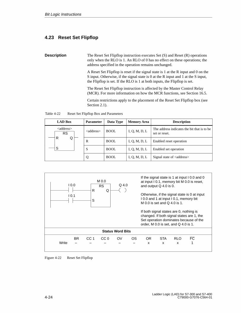
4-24Ladder Logic (LAD) for S7-300 and S7-400
C79000-G7076-C564-01
4.23 Reset Set Flipflop
The Reset Set Flipflop instruction executes Set (S) and Reset (R) operationsonly when the RLO is 1. An RLO of 0 has no effect on these operations; theaddress specified in the operation remains unchanged.
A Reset Set Flipflop is reset if the signal state is 1 at the R input and 0 on theS input. Otherwise, if the signal state is 0 at the R input and 1 at the S input,the Flipflop is set. If the RLO is 1 at both inputs, the Flipflop is set.
The Reset Set Flipflop instruction is affected by the Master Control Relay(MCR). For more information on how the MCR functions, see Section 16.5.
Certain restrictions apply to the placement of the Reset Set Flipflop box (seeSection 2.1).
Table 4-22 Reset Set Flipflop Box and Parameters
LAD Box Parameter Data Type Memory Area Description
RSR Q
<address><address> BOOL I, Q, M, D, L
The address indicates the bit that is to beset or reset.
R QR BOOL I, Q, M, D, L Enabled reset operation
S S BOOL I, Q, M, D, L Enabled set operation
Q BOOL I, Q, M, D, L Signal state of <address>
Status Word Bits
BR CC 1 CC 0 OV OS OR STA RLO FCWrite – – – – – x x x 1
I 0.0
If the signal state is 1 at input I 0.0 and 0at input I 0.1, memory bit M 0.0 is reset,and output Q 4.0 is 0.
Otherwise, if the signal state is 0 at inputI 0.0 and 1 at input I 0.1, memory bitM 0.0 is set and Q 4.0 is 1.
If both signal states are 0, nothing ischanged. If both signal states are 1, theSet operation dominates because of theorder, M 0.0 is set, and Q 4.0 is 1.
Q 4.0 M 0.0
RS
S
QR
I 0.1
Figure 4-22 Reset Set Flipflop
Description
Bit Logic Instructions
5-1Ladder Logic (LAD) for S7-300 and S7-400C79000-G7076-C564-01
Timer Instructions
Section Description Page
5.1 Location of a Timer in Memory and Components of a Timer 5-2
5.2 Choosing the Right Timer 5-4
5.3 Pulse S5 Timer 5-5
5.4 Extended Pulse S5 Timer 5-7
5.5 On-Delay S5 Timer 5-9
5.6 Retentive On-Delay S5 Timer 5-11
5.7 Off-Delay S5 Timer 5-13
Chapter Overview
5
5-2Ladder Logic (LAD) for S7-300 and S7-400
C79000-G7076-C564-01
5.1 Location of a Timer in Memory and Components of a Timer
Timers have an area reserved for them in the memory of your CPU. Thismemory area reserves one 16-bit word for each timer address. The ladderlogic instruction set supports 256 timers. Please refer to your CPU’s technicalinformation to establish the number of timer words available.
The following functions have access to the timer memory area:
� Timer instructions
� Updating of timer words by means of clock timing. This function of yourCPU in the RUN mode decrements a given time value by one unit at theinterval designated by the time base until the time value is equal to zero.
Bits 0 through 9 of the timer word contain the time value in binary code. Thetime value specifies a number of units. Time updating decrements the timevalue by one unit at an interval designated by the time base. Decrementingcontinues until the time value is equal to zero. You can load a time value intothe low word of accumulator 1 in binary, hexadecimal, or binary codeddecimal (BCD) format (see Figure 5-1). The time range is from 0 to 9,990seconds.
You can pre-load a time value using either of the following formats:
� W#16#wxyz
– Where w = the time base (that is, the time interval or resolution)
– Where xyz = the time value in binary coded decimal format
� S5T# aH_bbM_ccS_ddMS
– Where a = hours, bb = minutes, cc = seconds, and dd = milliseconds
– The time base is selected automatically, and the value is rounded tothe next lower number with that time base.
The maximum time value that you can enter is 9,990 seconds, or2H_46M_30S.
Bits 12 and 13 of the timer word contain the time base in binary code. Thetime base defines the interval at which the time value is decremented by oneunit (see Table 5-1 and Figure 5-1). The smallest time base is 10 ms; thelargest is 10 s.
Table 5-1 Time Base and Its Binary Code
Time Base Binary Code for the Time Base
10 ms 00
100 ms 01
1 s 10
10 s 11
Area in Memory
Time Value
Time Base
Timer Instructions
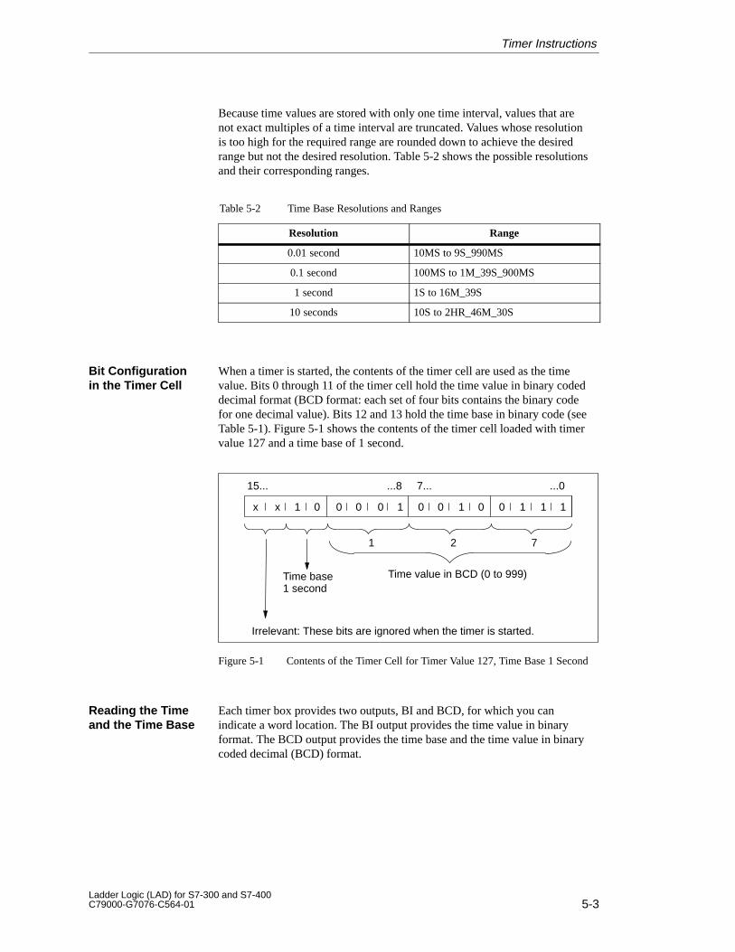
5-3Ladder Logic (LAD) for S7-300 and S7-400C79000-G7076-C564-01
Because time values are stored with only one time interval, values that arenot exact multiples of a time interval are truncated. Values whose resolutionis too high for the required range are rounded down to achieve the desiredrange but not the desired resolution. Table 5-2 shows the possible resolutionsand their corresponding ranges.
Table 5-2 Time Base Resolutions and Ranges
Resolution Range
0.01 second 10MS to 9S_990MS
0.1 second 100MS to 1M_39S_900MS
1 second 1S to 16M_39S
10 seconds 10S to 2HR_46M_30S
When a timer is started, the contents of the timer cell are used as the timevalue. Bits 0 through 11 of the timer cell hold the time value in binary codeddecimal format (BCD format: each set of four bits contains the binary codefor one decimal value). Bits 12 and 13 hold the time base in binary code (seeTable 5-1). Figure 5-1 shows the contents of the timer cell loaded with timervalue 127 and a time base of 1 second.
Time base1 second
Irrelevant: These bits are ignored when the timer is started.
Time value in BCD (0 to 999)
15... ...8 7... ...0
1 2 7
x x 1 0 0 0 0 1 0 0 1 0 0 1 1 1
Figure 5-1 Contents of the Timer Cell for Timer Value 127, Time Base 1 Second
Each timer box provides two outputs, BI and BCD, for which you canindicate a word location. The BI output provides the time value in binaryformat. The BCD output provides the time base and the time value in binarycoded decimal (BCD) format.
Bit Configurationin the Timer Cell
Reading the Timeand the Time Base
Timer Instructions
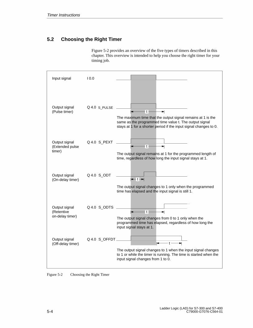
5-4Ladder Logic (LAD) for S7-300 and S7-400
C79000-G7076-C564-01
5.2 Choosing the Right Timer
Figure 5-2 provides an overview of the five types of timers described in thischapter. This overview is intended to help you choose the right timer for yourtiming job.
I 0.0
Q 4.0
S_PEXT
S_ODT
S_ODTS
S_OFFDT
Input signal
Output signal(Pulse timer) t
S_PULSE
t
t
t
t
The maximum time that the output signal remains at 1 is thesame as the programmed time value t. The output signalstays at 1 for a shorter period if the input signal changes to 0.
The output signal remains at 1 for the programmed length oftime, regardless of how long the input signal stays at 1.
The output signal changes to 1 only when the programmedtime has elapsed and the input signal is still 1.
The output signal changes from 0 to 1 only when theprogrammed time has elapsed, regardless of how long theinput signal stays at 1.
The output signal changes to 1 when the input signal changesto 1 or while the timer is running. The time is started when theinput signal changes from 1 to 0.
Q 4.0Output signal(Extended pulsetimer)
Q 4.0Output signal(On-delay timer)
Q 4.0Output signal(Retentiveon-delay timer)
Q 4.0Output signal(Off-delay timer)
Figure 5-2 Choosing the Right Timer
Timer Instructions
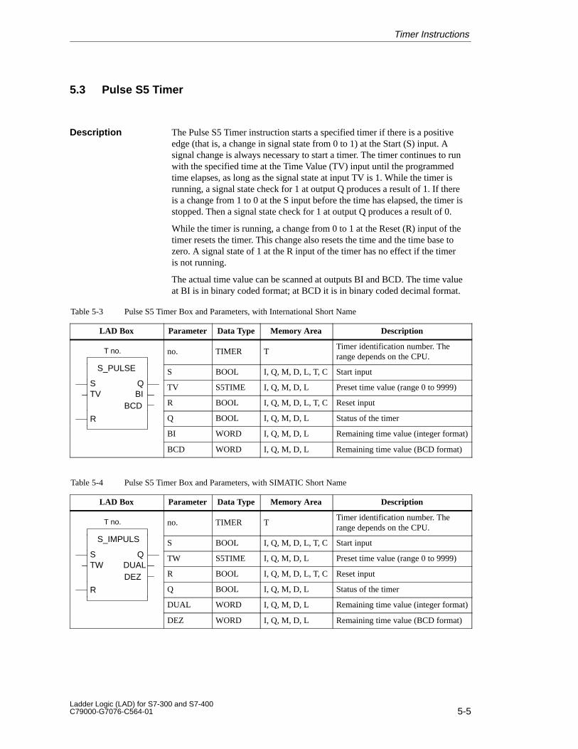
5-5Ladder Logic (LAD) for S7-300 and S7-400C79000-G7076-C564-01
5.3 Pulse S5 Timer
The Pulse S5 Timer instruction starts a specified timer if there is a positiveedge (that is, a change in signal state from 0 to 1) at the Start (S) input. Asignal change is always necessary to start a timer. The timer continues to runwith the specified time at the Time Value (TV) input until the programmedtime elapses, as long as the signal state at input TV is 1. While the timer isrunning, a signal state check for 1 at output Q produces a result of 1. If thereis a change from 1 to 0 at the S input before the time has elapsed, the timer isstopped. Then a signal state check for 1 at output Q produces a result of 0.
While the timer is running, a change from 0 to 1 at the Reset (R) input of thetimer resets the timer. This change also resets the time and the time base tozero. A signal state of 1 at the R input of the timer has no effect if the timeris not running.
The actual time value can be scanned at outputs BI and BCD. The time valueat BI is in binary coded format; at BCD it is in binary coded decimal format.
Table 5-3 Pulse S5 Timer Box and Parameters, with International Short Name
LAD Box Parameter Data Type Memory Area Description
T no.
S PULSE
no. TIMER TTimer identification number. Therange depends on the CPU.
S_PULSE
S QS BOOL I, Q, M, D, L, T, C Start input
STV BI
Q TV S5TIME I, Q, M, D, L Preset time value (range 0 to 9999)
BCDTV BI
R BOOL I, Q, M, D, L, T, C Reset input
R Q BOOL I, Q, M, D, L Status of the timer
BI WORD I, Q, M, D, L Remaining time value (integer format)
BCD WORD I, Q, M, D, L Remaining time value (BCD format)
Table 5-4 Pulse S5 Timer Box and Parameters, with SIMATIC Short Name
LAD Box Parameter Data Type Memory Area Description
T no.
S IMPULS
no. TIMER TTimer identification number. Therange depends on the CPU.
S_IMPULS
S QS BOOL I, Q, M, D, L, T, C Start input
STW DUAL
Q TW S5TIME I, Q, M, D, L Preset time value (range 0 to 9999)
DEZTW DUAL
R BOOL I, Q, M, D, L, T, C Reset input
R Q BOOL I, Q, M, D, L Status of the timer
DUAL WORD I, Q, M, D, L Remaining time value (integer format)
DEZ WORD I, Q, M, D, L Remaining time value (BCD format)
Description
Timer Instructions
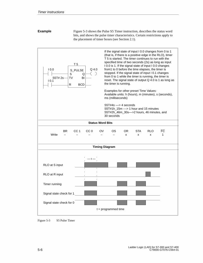
5-6Ladder Logic (LAD) for S7-300 and S7-400
C79000-G7076-C564-01
Figure 5-3 shows the Pulse S5 Timer instruction, describes the status wordbits, and shows the pulse timer characteristics. Certain restrictions apply tothe placement of timer boxes (see Section 2.1).
–– t ––
t = programmed time
I 0.0
If the signal state of input I 0.0 changes from 0 to 1(that is, if there is a positive edge in the RLO), timerT 5 is started. The timer continues to run with thespecified time of two seconds (2s) as long as inputI 0.0 is 1. If the signal state of input I 0.0 changesfrom1 to 0 before the time elapses, the timer isstopped. If the signal state of input I 0.1 changesfrom 0 to 1 while the timer is running, the timer isreset. The signal state of output Q 4.0 is 1 as long asthe timer is running.
Examples for other preset Time Values:Available units: h (hours), m (minutes), s (seconds),ms (milliseconds)
S5T#4s ––> 4 secondsS5T#1h_15m ––> 1 hour and 15 minutesS5T#2h_46m_30s––>2 hours, 46 minutes, and30 seconds
T 5
S_PULSE
R
QTV BI
BCD
S5T# 2s
Status Word Bits
BR CC 1 CC 0 OV OS OR STA RLO FCWrite – – – – – x x x 1
I 0.1
Q 4.0
S
Timing Diagram
RLO at S input
RLO at R input
Timer running
Signal state check for 1
Signal state check for 0
Figure 5-3 S5 Pulse Timer
Example
Timer Instructions
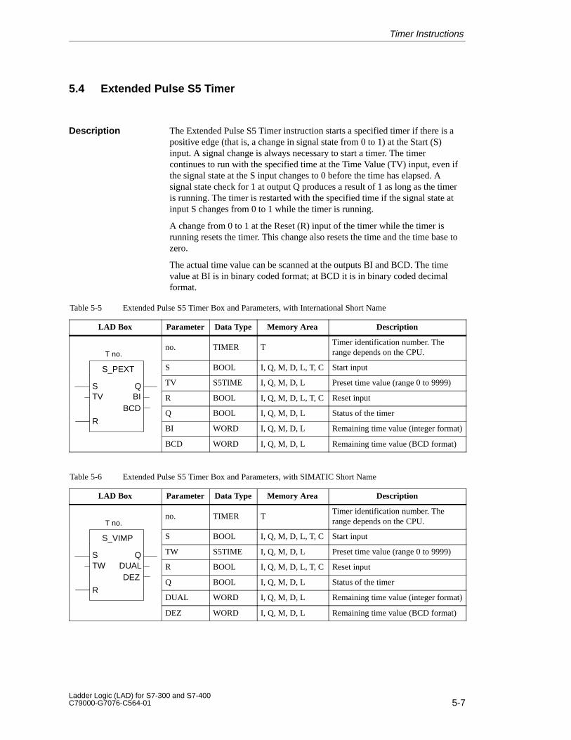
5-7Ladder Logic (LAD) for S7-300 and S7-400C79000-G7076-C564-01
5.4 Extended Pulse S5 Timer
The Extended Pulse S5 Timer instruction starts a specified timer if there is apositive edge (that is, a change in signal state from 0 to 1) at the Start (S)input. A signal change is always necessary to start a timer. The timercontinues to run with the specified time at the Time Value (TV) input, even ifthe signal state at the S input changes to 0 before the time has elapsed. Asignal state check for 1 at output Q produces a result of 1 as long as the timeris running. The timer is restarted with the specified time if the signal state atinput S changes from 0 to 1 while the timer is running.
A change from 0 to 1 at the Reset (R) input of the timer while the timer isrunning resets the timer. This change also resets the time and the time base tozero.
The actual time value can be scanned at the outputs BI and BCD. The timevalue at BI is in binary coded format; at BCD it is in binary coded decimalformat.
Table 5-5 Extended Pulse S5 Timer Box and Parameters, with International Short Name
LAD Box Parameter Data Type Memory Area Description
T no.no. TIMER T
Timer identification number. Therange depends on the CPU.
S_PEXT S BOOL I, Q, M, D, L, T, C Start input
S Q TV S5TIME I, Q, M, D, L Preset time value (range 0 to 9999)
BCD
STV BI
QR BOOL I, Q, M, D, L, T, C Reset input
BCD
RQ BOOL I, Q, M, D, L Status of the timer
RBI WORD I, Q, M, D, L Remaining time value (integer format)
BCD WORD I, Q, M, D, L Remaining time value (BCD format)
Table 5-6 Extended Pulse S5 Timer Box and Parameters, with SIMATIC Short Name
LAD Box Parameter Data Type Memory Area Description
T no.no. TIMER T
Timer identification number. Therange depends on the CPU.
S_VIMP S BOOL I, Q, M, D, L, T, C Start input
S Q TW S5TIME I, Q, M, D, L Preset time value (range 0 to 9999)
DEZ
STW DUAL
QR BOOL I, Q, M, D, L, T, C Reset input
DEZ
RQ BOOL I, Q, M, D, L Status of the timer
RDUAL WORD I, Q, M, D, L Remaining time value (integer format)
DEZ WORD I, Q, M, D, L Remaining time value (BCD format)
Description
Timer Instructions
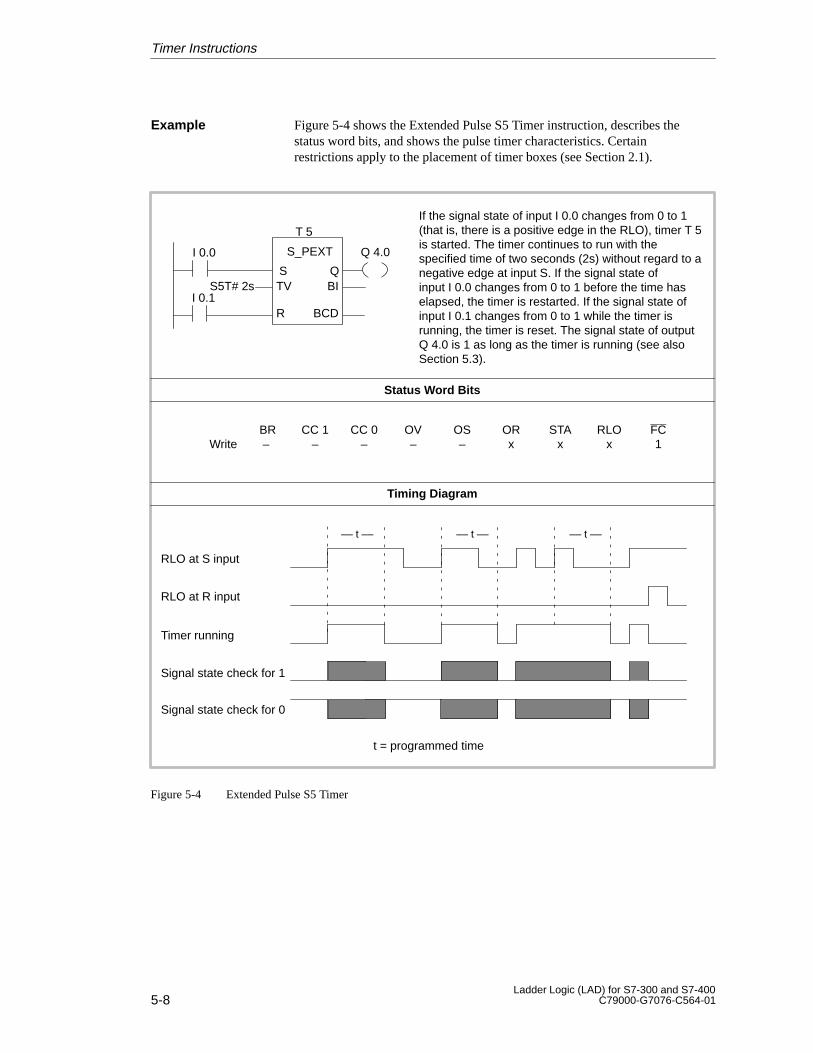
5-8Ladder Logic (LAD) for S7-300 and S7-400
C79000-G7076-C564-01
Figure 5-4 shows the Extended Pulse S5 Timer instruction, describes thestatus word bits, and shows the pulse timer characteristics. Certainrestrictions apply to the placement of timer boxes (see Section 2.1).
–– t –– –– t –– –– t ––
t = programmed time
Status Word Bits
Timing Diagram
BR CC 1 CC 0 OV OS OR STA RLO FCWrite – – – – – x x x 1
If the signal state of input I 0.0 changes from 0 to 1(that is, there is a positive edge in the RLO), timer T 5is started. The timer continues to run with thespecified time of two seconds (2s) without regard to anegative edge at input S. If the signal state ofinput I 0.0 changes from 0 to 1 before the time haselapsed, the timer is restarted. If the signal state ofinput I 0.1 changes from 0 to 1 while the timer isrunning, the timer is reset. The signal state of outputQ 4.0 is 1 as long as the timer is running (see alsoSection 5.3).
I 0.0
T 5
S_PEXT
R
QTV BI
BCD
S5T# 2sI 0.1
Q 4.0
S
RLO at S input
RLO at R input
Timer running
Signal state check for 1
Signal state check for 0
Figure 5-4 Extended Pulse S5 Timer
Example
Timer Instructions
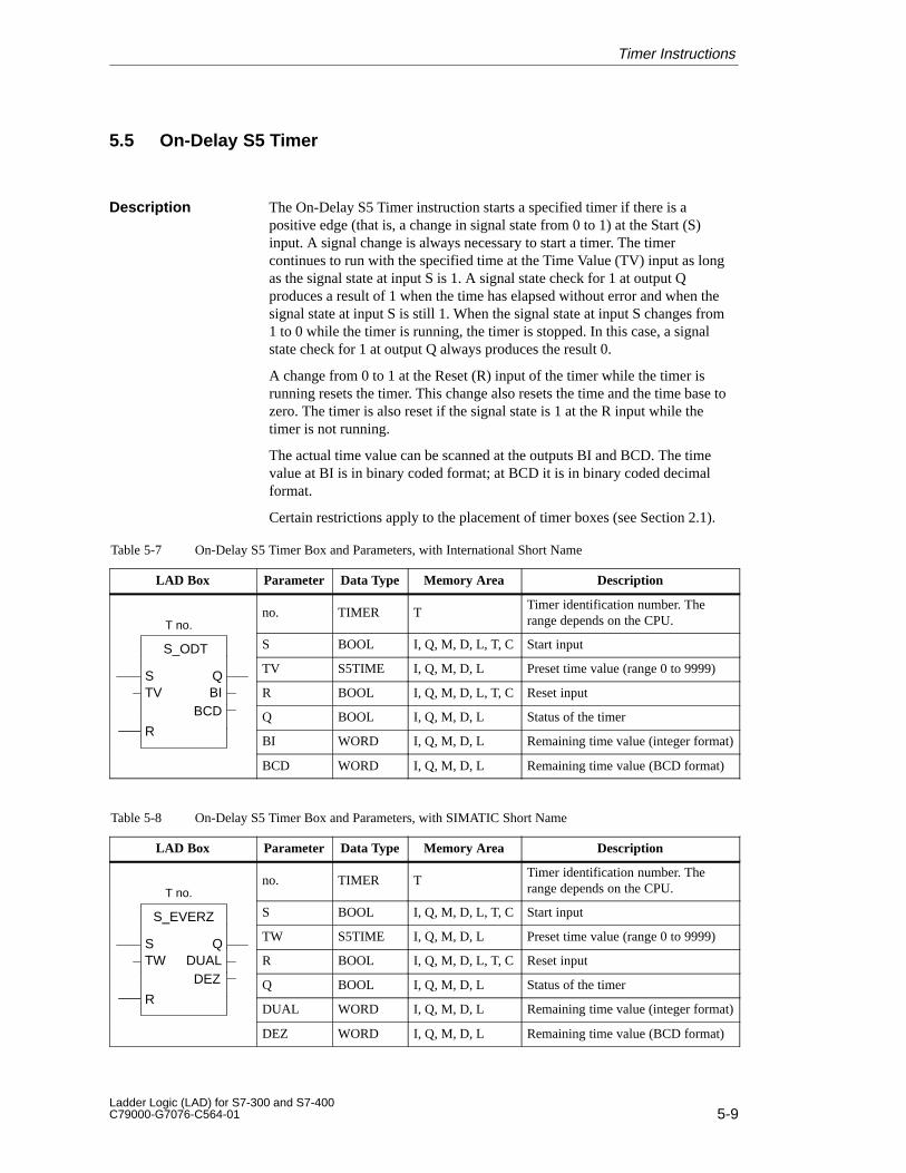
5-9Ladder Logic (LAD) for S7-300 and S7-400C79000-G7076-C564-01
5.5 On-Delay S5 Timer
The On-Delay S5 Timer instruction starts a specified timer if there is apositive edge (that is, a change in signal state from 0 to 1) at the Start (S)input. A signal change is always necessary to start a timer. The timercontinues to run with the specified time at the Time Value (TV) input as longas the signal state at input S is 1. A signal state check for 1 at output Qproduces a result of 1 when the time has elapsed without error and when thesignal state at input S is still 1. When the signal state at input S changes from1 to 0 while the timer is running, the timer is stopped. In this case, a signalstate check for 1 at output Q always produces the result 0.
A change from 0 to 1 at the Reset (R) input of the timer while the timer isrunning resets the timer. This change also resets the time and the time base tozero. The timer is also reset if the signal state is 1 at the R input while thetimer is not running.
The actual time value can be scanned at the outputs BI and BCD. The timevalue at BI is in binary coded format; at BCD it is in binary coded decimalformat.
Certain restrictions apply to the placement of timer boxes (see Section 2.1).
Table 5-7 On-Delay S5 Timer Box and Parameters, with International Short Name
LAD Box Parameter Data Type Memory Area Description
T no.no. TIMER T
Timer identification number. Therange depends on the CPU.
S_ODT S BOOL I, Q, M, D, L, T, C Start input_
S Q TV S5TIME I, Q, M, D, L Preset time value (range 0 to 9999)
BCD
STV BI
QR BOOL I, Q, M, D, L, T, C Reset input
BCD
RQ BOOL I, Q, M, D, L Status of the timer
RBI WORD I, Q, M, D, L Remaining time value (integer format)
BCD WORD I, Q, M, D, L Remaining time value (BCD format)
Table 5-8 On-Delay S5 Timer Box and Parameters, with SIMATIC Short Name
LAD Box Parameter Data Type Memory Area Description
T no.no. TIMER T
Timer identification number. Therange depends on the CPU.
S_EVERZ S BOOL I, Q, M, D, L, T, C Start input_
S Q TW S5TIME I, Q, M, D, L Preset time value (range 0 to 9999)
DEZ
STW DUAL
QR BOOL I, Q, M, D, L, T, C Reset input
DEZ
RQ BOOL I, Q, M, D, L Status of the timer
RDUAL WORD I, Q, M, D, L Remaining time value (integer format)
DEZ WORD I, Q, M, D, L Remaining time value (BCD format)
Description
Timer Instructions
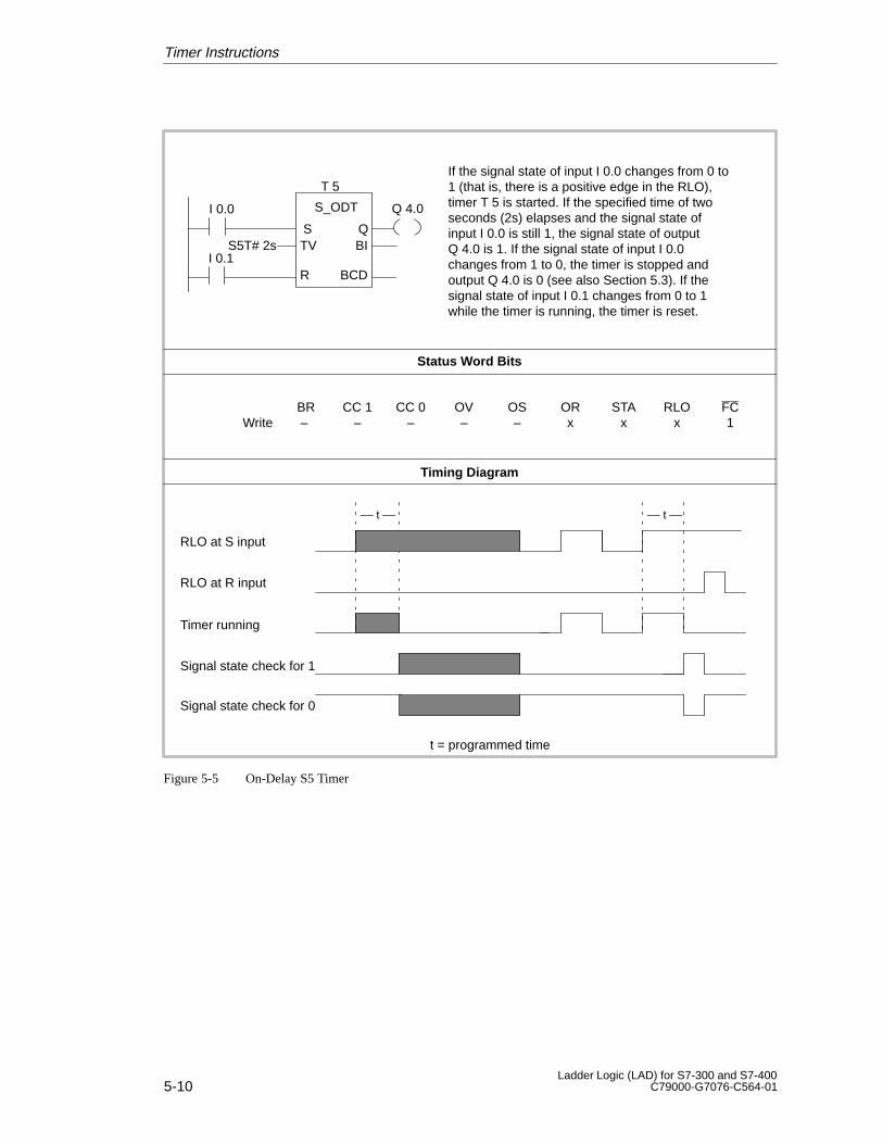
5-10Ladder Logic (LAD) for S7-300 and S7-400
C79000-G7076-C564-01
–– t –– –– t ––
t = programmed time
If the signal state of input I 0.0 changes from 0 to1 (that is, there is a positive edge in the RLO),timer T 5 is started. If the specified time of twoseconds (2s) elapses and the signal state ofinput I 0.0 is still 1, the signal state of outputQ 4.0 is 1. If the signal state of input I 0.0changes from 1 to 0, the timer is stopped andoutput Q 4.0 is 0 (see also Section 5.3). If thesignal state of input I 0.1 changes from 0 to 1while the timer is running, the timer is reset.
I 0.0
T 5
S_ODT
R
QTV BI
BCD
S5T# 2sI 0.1
Q 4.0
S
Status Word Bits
Timing Diagram
BR CC 1 CC 0 OV OS OR STA RLO FCWrite – – – – – x x x 1
RLO at S input
RLO at R input
Timer running
Signal state check for 1
Signal state check for 0
Figure 5-5 On-Delay S5 Timer
Timer Instructions
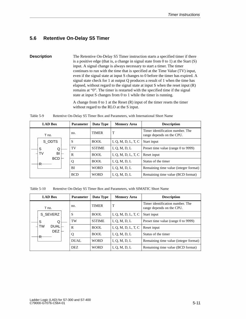
5-11Ladder Logic (LAD) for S7-300 and S7-400C79000-G7076-C564-01
5.6 Retentive On-Delay S5 Timer
The Retentive On-Delay S5 Timer instruction starts a specified timer if thereis a positive edge (that is, a change in signal state from 0 to 1) at the Start (S)input. A signal change is always necessary to start a timer. The timercontinues to run with the time that is specified at the Time Value (TV) input,even if the signal state at input S changes to 0 before the timer has expired. Asignal state check for 1 at output Q produces a result of 1 when the time haselapsed, without regard to the signal state at input S when the reset input (R)remains at “0”. The timer is restarted with the specified time if the signalstate at input S changes from 0 to 1 while the timer is running.
A change from 0 to 1 at the Reset (R) input of the timer resets the timerwithout regard to the RLO at the S input.
Table 5-9 Retentive On-Delay S5 Timer Box and Parameters, with International Short Name
LAD Box Parameter Data Type Memory Area Description
T no.no. TIMER T
Timer identification number. Therange depends on the CPU.
S_ODTS S BOOL I, Q, M, D, L, T, C Start input
S Q TV S5TIME I, Q, M, D, L Preset time value (range 0 to 9999)
BCDTV BI R BOOL I, Q, M, D, L, T, C Reset input
BCD
RQ BOOL I, Q, M, D, L Status of the timer
RBI WORD I, Q, M, D, L Remaining time value (integer format)
BCD WORD I, Q, M, D, L Remaining time value (BCD format)
Table 5-10 Retentive On-Delay S5 Timer Box and Parameters, with SIMATIC Short Name
LAD Box Parameter Data Type Memory Area Description
T no.no. TIMER T
Timer identification number. Therange depends on the CPU.
S_SEVERZ S BOOL I, Q, M, D, L, T, C Start input
S Q TW S5TIME I, Q, M, D, L Preset time value (range 0 to 9999)
DEZTW DUAL R BOOL I, Q, M, D, L, T, C Reset input
DEZ
RQ BOOL I, Q, M, D, L Status of the timer
RDUAL WORD I, Q, M, D, L Remaining time value (integer format)
DEZ WORD I, Q, M, D, L Remaining time value (BCD format)
Description
Timer Instructions
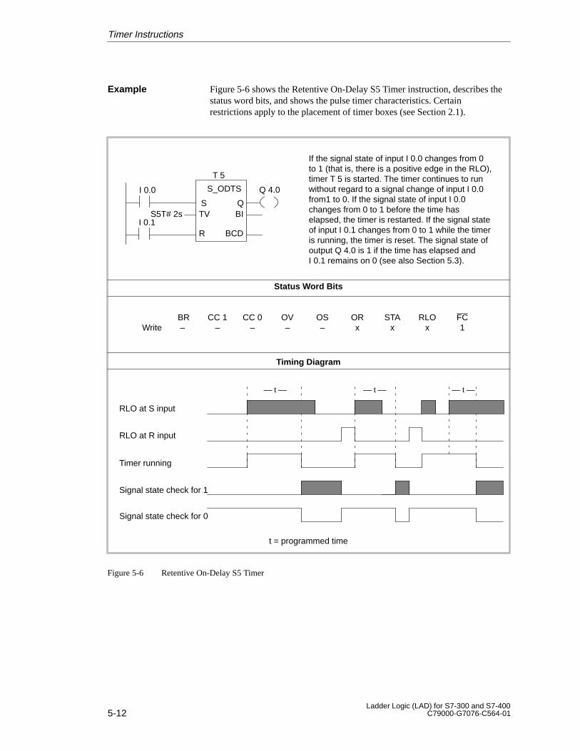
5-12Ladder Logic (LAD) for S7-300 and S7-400
C79000-G7076-C564-01
Figure 5-6 shows the Retentive On-Delay S5 Timer instruction, describes thestatus word bits, and shows the pulse timer characteristics. Certainrestrictions apply to the placement of timer boxes (see Section 2.1).
–– t –– –– t ––
t = programmed time
–– t ––
If the signal state of input I 0.0 changes from 0to 1 (that is, there is a positive edge in the RLO),timer T 5 is started. The timer continues to runwithout regard to a signal change of input I 0.0from1 to 0. If the signal state of input I 0.0changes from 0 to 1 before the time haselapsed, the timer is restarted. If the signal stateof input I 0.1 changes from 0 to 1 while the timeris running, the timer is reset. The signal state ofoutput Q 4.0 is 1 if the time has elapsed andI 0.1 remains on 0 (see also Section 5.3).
I 0.0
T 5
S_ODTS
R
QTV BI
BCD
S5T# 2sI 0.1
Q 4.0
S
RLO at S input
RLO at R input
Timer running
Signal state check for 1
Signal state check for 0
BR CC 1 CC 0 OV OS OR STA RLO FCWrite – – – – – x x x 1
Status Word Bits
Timing Diagram
Figure 5-6 Retentive On-Delay S5 Timer
Example
Timer Instructions
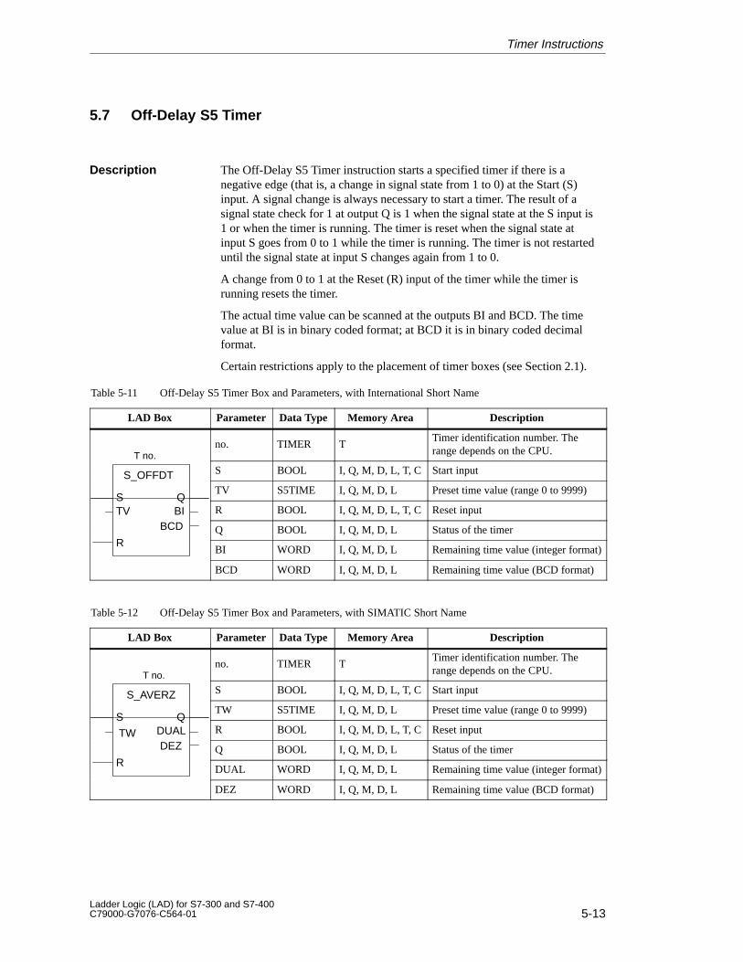
5-13Ladder Logic (LAD) for S7-300 and S7-400C79000-G7076-C564-01
5.7 Off-Delay S5 Timer
The Off-Delay S5 Timer instruction starts a specified timer if there is anegative edge (that is, a change in signal state from 1 to 0) at the Start (S)input. A signal change is always necessary to start a timer. The result of asignal state check for 1 at output Q is 1 when the signal state at the S input is1 or when the timer is running. The timer is reset when the signal state atinput S goes from 0 to 1 while the timer is running. The timer is not restarteduntil the signal state at input S changes again from 1 to 0.
A change from 0 to 1 at the Reset (R) input of the timer while the timer isrunning resets the timer.
The actual time value can be scanned at the outputs BI and BCD. The timevalue at BI is in binary coded format; at BCD it is in binary coded decimalformat.
Certain restrictions apply to the placement of timer boxes (see Section 2.1).
Table 5-11 Off-Delay S5 Timer Box and Parameters, with International Short Name
LAD Box Parameter Data Type Memory Area Description
T no.no. TIMER T
Timer identification number. Therange depends on the CPU. T no.
S_OFFDT S BOOL I, Q, M, D, L, T, C Start inputS_OFFDT
S QTV S5TIME I, Q, M, D, L Preset time value (range 0 to 9999)
STV BI
QR BOOL I, Q, M, D, L, T, C Reset input
BCD
RQ BOOL I, Q, M, D, L Status of the timer
RBI WORD I, Q, M, D, L Remaining time value (integer format)
BCD WORD I, Q, M, D, L Remaining time value (BCD format)
Table 5-12 Off-Delay S5 Timer Box and Parameters, with SIMATIC Short Name
LAD Box Parameter Data Type Memory Area Description
T no.no. TIMER T
Timer identification number. Therange depends on the CPU. T no.
S_AVERZ S BOOL I, Q, M, D, L, T, C Start inputS_AVERZ
S QTW S5TIME I, Q, M, D, L Preset time value (range 0 to 9999)
S
TW DUALQ
R BOOL I, Q, M, D, L, T, C Reset input
DEZ
RQ BOOL I, Q, M, D, L Status of the timer
RDUAL WORD I, Q, M, D, L Remaining time value (integer format)
DEZ WORD I, Q, M, D, L Remaining time value (BCD format)
Description
Timer Instructions
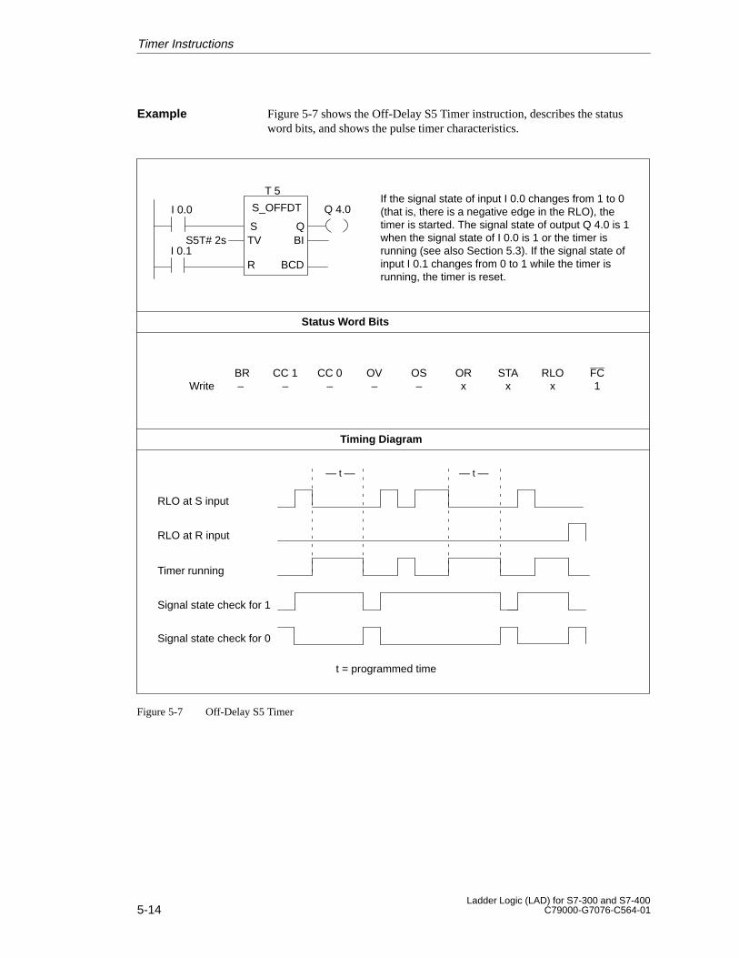
5-14Ladder Logic (LAD) for S7-300 and S7-400
C79000-G7076-C564-01
Figure 5-7 shows the Off-Delay S5 Timer instruction, describes the statusword bits, and shows the pulse timer characteristics.
If the signal state of input I 0.0 changes from 1 to 0(that is, there is a negative edge in the RLO), thetimer is started. The signal state of output Q 4.0 is 1when the signal state of I 0.0 is 1 or the timer isrunning (see also Section 5.3). If the signal state ofinput I 0.1 changes from 0 to 1 while the timer isrunning, the timer is reset.
Status Word Bits
BR CC 1 CC 0 OV OS OR STA RLO FCWrite – – – – – x x x 1
Timing Diagram
RLO at S input
RLO at R input
Timer running
Signal state check for 1
Signal state check for 0
t = programmed time
–– t –– –– t ––
I 0.0
T 5
S_OFFDT
R
QTV BI
BCD
S5T# 2sI 0.1
Q 4.0
S
Figure 5-7 Off-Delay S5 Timer
Example
Timer Instructions
6-1Ladder Logic (LAD) for S7-300 and S7-400C79000-G7076-C564-01
Counter Instructions
Section Description Page
6.1 Location of a Counter in Memory and Components of aCounter
6-2
6.2 Up-Down Counter 6-3
6.3 Up Counter 6-5
6.4 Down Counter 6-7
Chapter Overview
6
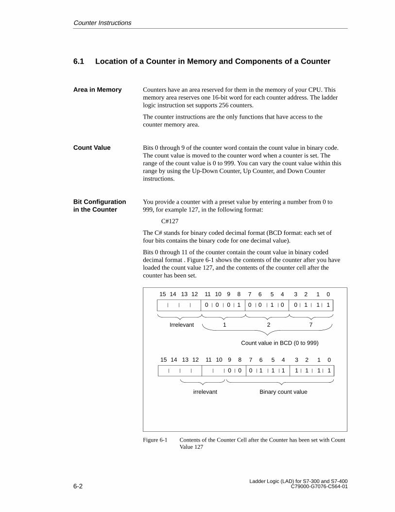
6-2Ladder Logic (LAD) for S7-300 and S7-400
C79000-G7076-C564-01
6.1 Location of a Counter in Memory and Components of a Counter
Counters have an area reserved for them in the memory of your CPU. Thismemory area reserves one 16-bit word for each counter address. The ladderlogic instruction set supports 256 counters.
The counter instructions are the only functions that have access to thecounter memory area.
Bits 0 through 9 of the counter word contain the count value in binary code.The count value is moved to the counter word when a counter is set. Therange of the count value is 0 to 999. You can vary the count value within thisrange by using the Up-Down Counter, Up Counter, and Down Counterinstructions.
You provide a counter with a preset value by entering a number from 0 to999, for example 127, in the following format:
C#127
The C# stands for binary coded decimal format (BCD format: each set offour bits contains the binary code for one decimal value).
Bits 0 through 11 of the counter contain the count value in binary codeddecimal format . Figure 6-1 shows the contents of the counter after you haveloaded the count value 127, and the contents of the counter cell after thecounter has been set.
Irrelevant
15
1 2 7
14 13 12 11 10 9 8 7 6 5 4 3 2 1 0
1 111 10000000
15 14 13 12 11 10 9 8 7 6 5 4 3 2 1 0
1 110 111100
irrelevant Binary count value
Count value in BCD (0 to 999)
Figure 6-1 Contents of the Counter Cell after the Counter has been set with CountValue 127
Area in Memory
Count Value
Bit Configurationin the Counter
Counter Instructions
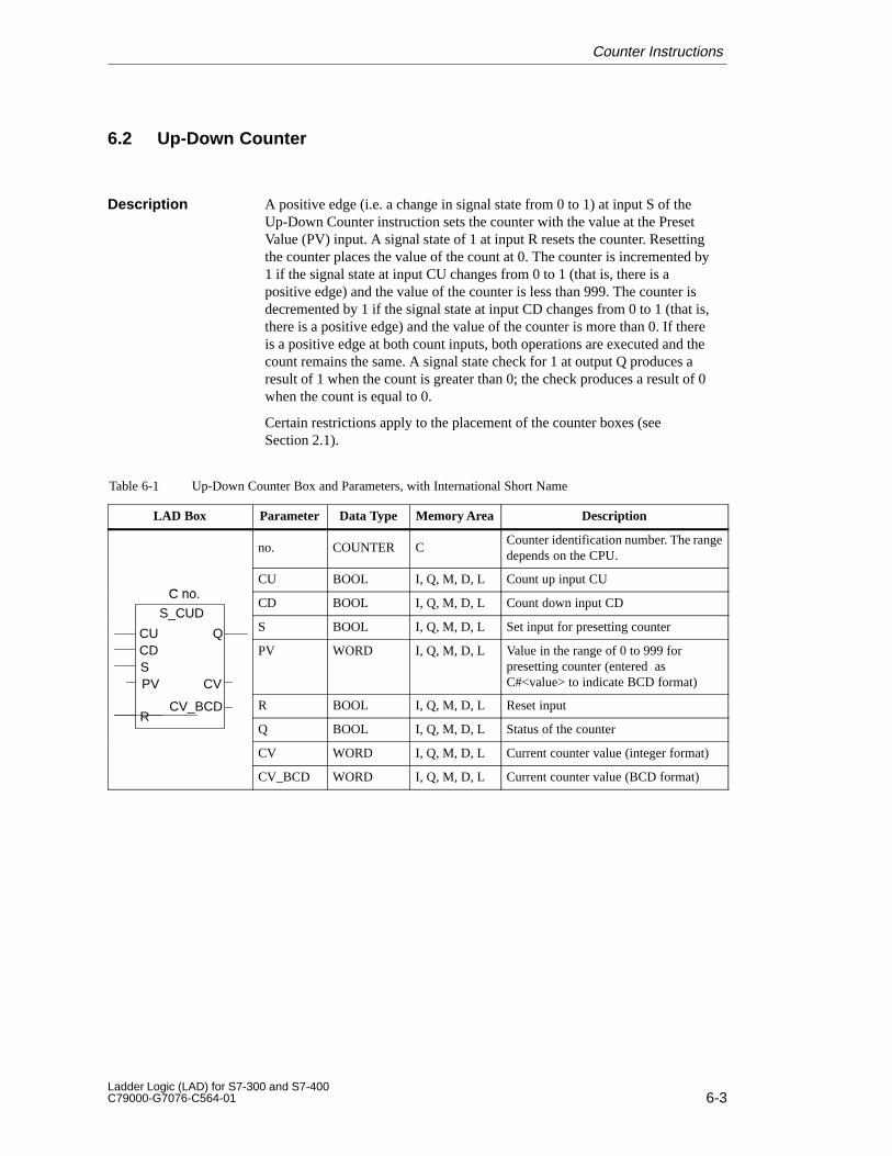
6-3Ladder Logic (LAD) for S7-300 and S7-400C79000-G7076-C564-01
6.2 Up-Down Counter
A positive edge (i.e. a change in signal state from 0 to 1) at input S of theUp-Down Counter instruction sets the counter with the value at the PresetValue (PV) input. A signal state of 1 at input R resets the counter. Resettingthe counter places the value of the count at 0. The counter is incremented by1 if the signal state at input CU changes from 0 to 1 (that is, there is apositive edge) and the value of the counter is less than 999. The counter isdecremented by 1 if the signal state at input CD changes from 0 to 1 (that is,there is a positive edge) and the value of the counter is more than 0. If thereis a positive edge at both count inputs, both operations are executed and thecount remains the same. A signal state check for 1 at output Q produces aresult of 1 when the count is greater than 0; the check produces a result of 0when the count is equal to 0.
Certain restrictions apply to the placement of the counter boxes (seeSection 2.1).
Table 6-1 Up-Down Counter Box and Parameters, with International Short Name
LAD Box Parameter Data Type Memory Area Description
C
no. COUNTER CCounter identification number. The rangedepends on the CPU.
C noCU BOOL I, Q, M, D, L Count up input CU
C no.
S CUDCD BOOL I, Q, M, D, L Count down input CD
S_CUD
QCU S BOOL I, Q, M, D, L Set input for presetting counter
CV
QCUCDSPV
PV WORD I, Q, M, D, L Value in the range of 0 to 999 forpresetting counter (entered asC#<value> to indicate BCD format)
CV_BCDR
R BOOL I, Q, M, D, L Reset inputR
Q BOOL I, Q, M, D, L Status of the counter
CV WORD I, Q, M, D, L Current counter value (integer format)
CV_BCD WORD I, Q, M, D, L Current counter value (BCD format)
Description
Counter Instructions
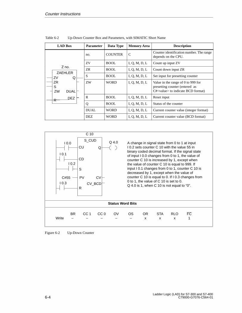
6-4Ladder Logic (LAD) for S7-300 and S7-400
C79000-G7076-C564-01
Table 6-2 Up-Down Counter Box and Parameters, with SIMATIC Short Name
LAD Box Parameter Data Type Memory Area Description
Z
no. COUNTER CCounter identification number. The rangedepends on the CPU.
Z noZV BOOL I, Q, M, D, L Count up input ZV
Z no.
ZAEHLERZR BOOL I, Q, M, D, L Count down input ZR
ZAEHLERQZV S BOOL I, Q, M, D, L Set input for presetting counter
DUAL
QZVZRSZW
ZW WORD I, Q, M, D, L Value in the range of 0 to 999 forpresetting counter (entered asC#<value> to indicate BCD format)
DEZRR BOOL I, Q, M, D, L Reset input
RQ BOOL I, Q, M, D, L Status of the counter
DUAL WORD I, Q, M, D, L Current counter value (integer format)
DEZ WORD I, Q, M, D, L Current counter value (BCD format)
A change in signal state from 0 to 1 at inputI 0.2 sets counter C 10 with the value 55 inbinary coded decimal format. If the signal stateof input I 0.0 changes from 0 to 1, the value ofcounter C 10 is increased by 1, except whenthe value of counter C 10 is equal to 999. Ifinput I 0.1 changes from 0 to 1, counter C 10 isdecreased by 1, except when the value ofcounter C 10 is equal to 0. If I 0.3 changes from0 to 1, the value of C 10 is set to 0. Q 4.0 is 1, when C 10 is not equal to “0”.
Status Word Bits
BR CC 1 CC 0 OV OS OR STA RLO FCWrite – – – – – x x x 1
C 10
S_CUD
CV
QCU
CD
CV_BCD
S
PV
R
I 0.0 Q 4.0
I 0.1
I 0.2
C#55
I 0.3
Figure 6-2 Up-Down Counter
Counter Instructions
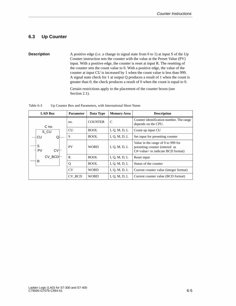
6-5Ladder Logic (LAD) for S7-300 and S7-400C79000-G7076-C564-01
6.3 Up Counter
A positive edge (i.e. a change in signal state from 0 to 1) at input S of the UpCounter instruction sets the counter with the value at the Preset Value (PV)input. With a positive edge, the counter is reset at input R. The resetting ofthe counter sets the count value to 0. With a positive edge, the value of thecounter at input CU is increased by 1 when the count value is less than 999.A signal state check for 1 at output Q produces a result of 1 when the count isgreater than 0; the check produces a result of 0 when the count is equal to 0.
Certain restrictions apply to the placement of the counter boxes (seeSection 2.1).
Table 6-3 Up Counter Box and Parameters, with International Short Name
LAD Box Parameter Data Type Memory Area Description
C no.no. COUNTER C
Counter identification number. The rangedepends on the CPU.
C no.
S_CU CU BOOL I, Q, M, D, L Count up input CUS_CU
QCU S BOOL I, Q, M, D, L Set input for presetting counter
CVSPV
PV WORD I, Q, M, D, LValue in the range of 0 to 999 forpresetting counter (entered asC#<value> to indicate BCD format)
CV_BCDR
R BOOL I, Q, M, D, L Reset inputR
Q BOOL I, Q, M, D, L Status of the counter
CV WORD I, Q, M, D, L Current counter value (integer format)
CV_BCD WORD I, Q, M, D, L Current counter value (BCD format)
Description
Counter Instructions
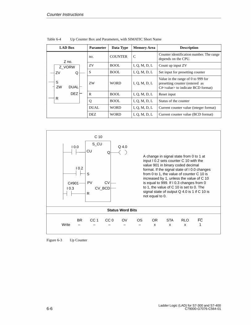
6-6Ladder Logic (LAD) for S7-300 and S7-400
C79000-G7076-C564-01
Table 6-4 Up Counter Box and Parameters, with SIMATIC Short Name
LAD Box Parameter Data Type Memory Area Description
Z no.no. COUNTER C
Counter identification number. The rangedepends on the CPU.
Z no.
Z_VORW ZV BOOL I, Q, M, D, L Count up input ZVZ_VORW
QZV S BOOL I, Q, M, D, L Set input for presetting counter
DUALSZW
ZW WORD I, Q, M, D, LValue in the range of 0 to 999 forpresetting counter (entered asC#<value> to indicate BCD format)
DEZR
R BOOL I, Q, M, D, L Reset inputR
Q BOOL I, Q, M, D, L Status of the counter
DUAL WORD I, Q, M, D, L Current counter value (integer format)
DEZ WORD I, Q, M, D, L Current counter value (BCD format)
Status Word Bits
BR CC 1 CC 0 OV OS OR STA RLO FCWrite – – – – – x x x 1
A change in signal state from 0 to 1 atinput I 0.2 sets counter C 10 with thevalue 901 in binary coded decimalformat. If the signal state of I 0.0 changesfrom 0 to 1, the value of counter C 10 isincreased by 1, unless the value of C 10is equal to 999. If I 0.3 changes from 0to 1, the value of C 10 is set to 0. Thesignal state of output Q 4.0 is 1 if C 10 isnot equal to 0.
C 10
S_CU
CV
QCU
CV_BCD
S
PV
R
I 0.0 Q 4.0
I 0.2
C#901I 0.3
Figure 6-3 Up Counter
Counter Instructions
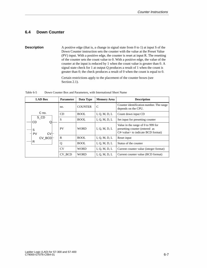
6-7Ladder Logic (LAD) for S7-300 and S7-400C79000-G7076-C564-01
6.4 Down Counter
A positive edge (that is, a change in signal state from 0 to 1) at input S of theDown Counter instruction sets the counter with the value at the Preset Value(PV) input. With a positive edge, the counter is reset at input R. The resettingof the counter sets the count value to 0. With a positive edge, the value of thecounter at the input is reduced by 1 when the count value is greater than 0. Asignal state check for 1 at output Q produces a result of 1 when the count isgreater than 0; the check produces a result of 0 when the count is equal to 0.
Certain restrictions apply to the placement of the counter boxes (seeSection 2.1).
Table 6-5 Down Counter Box and Parameters, with International Short Name
LAD Box Parameter Data Type Memory Area Description
C
no. COUNTER CCounter identification number. The rangedepends on the CPU.
C no.
S CDCD BOOL I, Q, M, D, L Count down input CD
S_CD
QCDS BOOL I, Q, M, D, L Set input for presetting counter
CV
QCD
SPV
PV WORD I, Q, M, D, LValue in the range of 0 to 999 forpresetting counter (entered asC#<value> to indicate BCD format)CV
CV_BCDPV
RR BOOL I, Q, M, D, L Reset input
R Q BOOL I, Q, M, D, L Status of the counter
CV WORD I, Q, M, D, L Current counter value (integer format)
CV_BCD WORD I, Q, M, D, L Current counter value (BCD format)
Description
Counter Instructions
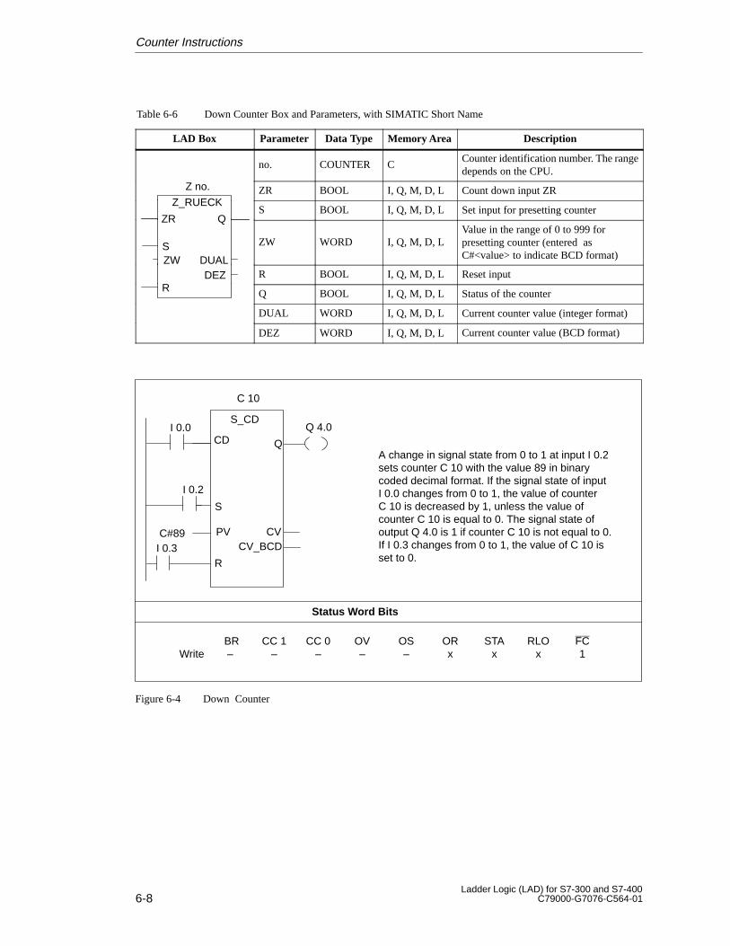
6-8Ladder Logic (LAD) for S7-300 and S7-400
C79000-G7076-C564-01
Table 6-6 Down Counter Box and Parameters, with SIMATIC Short Name
LAD Box Parameter Data Type Memory Area Description
Z
no. COUNTER CCounter identification number. The rangedepends on the CPU.
Z no.
Z RUECKZR BOOL I, Q, M, D, L Count down input ZR
Z_RUECK
QZRS BOOL I, Q, M, D, L Set input for presetting counter
DUAL
QZR
SZW
ZW WORD I, Q, M, D, LValue in the range of 0 to 999 forpresetting counter (entered asC#<value> to indicate BCD format)DUAL
DEZZW
RR BOOL I, Q, M, D, L Reset input
R Q BOOL I, Q, M, D, L Status of the counter
DUAL WORD I, Q, M, D, L Current counter value (integer format)
DEZ WORD I, Q, M, D, L Current counter value (BCD format)
Status Word Bits
BR CC 1 CC 0 OV OS OR STA RLO FCWrite – – – – – x x x 1
A change in signal state from 0 to 1 at input I 0.2sets counter C 10 with the value 89 in binarycoded decimal format. If the signal state of inputI 0.0 changes from 0 to 1, the value of counterC 10 is decreased by 1, unless the value ofcounter C 10 is equal to 0. The signal state ofoutput Q 4.0 is 1 if counter C 10 is not equal to 0.If I 0.3 changes from 0 to 1, the value of C 10 isset to 0.
C 10
S_CD
CV
QCD
CV_BCD
S
PV
R
I 0.0 Q 4.0
I 0.2
C#89I 0.3
Figure 6-4 Down Counter
Counter Instructions

7-1Ladder Logic (LAD) for S7-300 and S7-400C79000-G7076-C564-01
Integer Math Instructions
Section Description Page
7.1 Add Integer 7-2
7.2 Add Double Integer 7-3
7.3 Subtract Integer 7-4
7.4 Subtract Double Integer 7-5
7.5 Multiply Integer 7-6
7.6 Multiply Double Integer 7-7
7.7 Divide Integer 7-8
7.8 Divide Double Integer 7-9
7.9 Return Fraction Double Integer 7-10
7.10 Evaluating the Bits of the Status Word After Integer MathInstructions
7-11
Chapter Overview
7
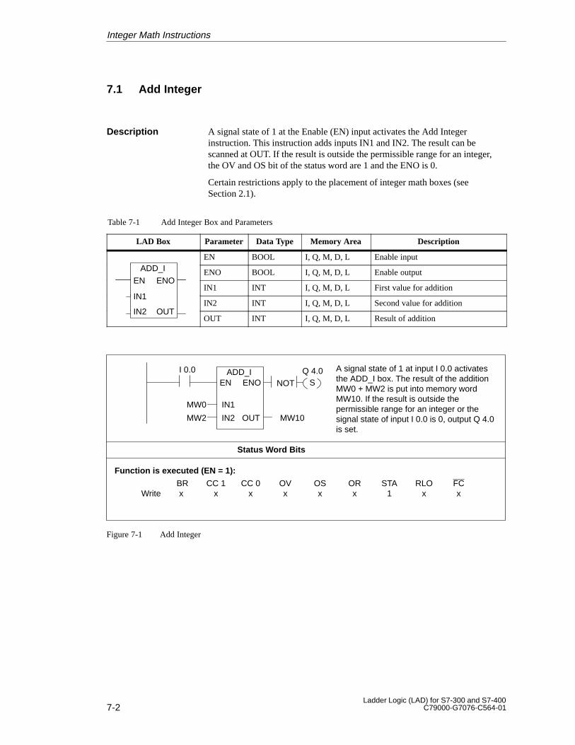
7-2Ladder Logic (LAD) for S7-300 and S7-400
C79000-G7076-C564-01
7.1 Add Integer
A signal state of 1 at the Enable (EN) input activates the Add Integerinstruction. This instruction adds inputs IN1 and IN2. The result can bescanned at OUT. If the result is outside the permissible range for an integer,the OV and OS bit of the status word are 1 and the ENO is 0.
Certain restrictions apply to the placement of integer math boxes (seeSection 2.1).
Table 7-1 Add Integer Box and Parameters
LAD Box Parameter Data Type Memory Area Description
ADD IEN BOOL I, Q, M, D, L Enable input
ADD_I
EN ENOENO BOOL I, Q, M, D, L Enable output
IN1
EN ENOIN1 INT I, Q, M, D, L First value for addition
IN1
IN2 OUTIN2 INT I, Q, M, D, L Second value for addition
IN2 OUTOUT INT I, Q, M, D, L Result of addition
Status Word Bits
BR CC 1 CC 0 OV OS OR STA RLO FCWrite x x x x x x 1 x x
I 0.0 A signal state of 1 at input I 0.0 activatesthe ADD_I box. The result of the additionMW0 + MW2 is put into memory wordMW10. If the result is outside thepermissible range for an integer or thesignal state of input I 0.0 is 0, output Q 4.0is set.
Q 4.0ADD_I
IN2
EN ENO
MW2 MW10
IN1MW0
S
Function is executed (EN = 1):
NOT
OUT
Figure 7-1 Add Integer
Description
Integer Math Instructions
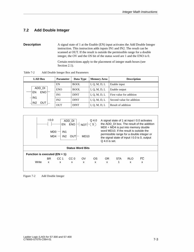
7-3Ladder Logic (LAD) for S7-300 and S7-400C79000-G7076-C564-01
7.2 Add Double Integer
A signal state of 1 at the Enable (EN) input activates the Add Double Integerinstruction. This instruction adds inputs IN1 and IN2. The result can bescanned at OUT. If the result is outside the permissible range for a doubleinteger, the OV and the OS bit of the status word are 1 and the ENO is 0.
Certain restrictions apply to the placement of integer math boxes (seeSection 2.1).
Table 7-2 Add Double Integer Box and Parameters
LAD Box Parameter Data Type Memory Area Description
ADD DIEN BOOL I, Q, M, D, L Enable input
ADD_DI
EN ENOENO BOOL I, Q, M, D, L Enable output
IN1
EN ENOIN1 DINT I, Q, M, D, L First value for addition
IN1
IN2 OUTIN2 DINT I, Q, M, D, L Second value for addition
IN2 OUTOUT DINT I, Q, M, D, L Result of addition
Status Word Bits
BR CC 1 CC 0 OV OS OR STA RLO FCWrite x x x x x x 1 x x
I 0.0 A signal state of 1 at input I 0.0 activatesthe ADD_DI box. The result of the additionMD0 + MD4 is put into memory doubleword MD10. If the result is outside thepermissible range for a double integer orthe signal state of input I 0.0 is 0, outputQ 4.0 is set.
Q 4.0ADD_DI
IN2
EN ENO
MD4 MD10
IN1MD0
S
Function is executed (EN = 1):
NOT
OUT
Figure 7-2 Add Double Integer
Description
Integer Math Instructions

7-4Ladder Logic (LAD) for S7-300 and S7-400
C79000-G7076-C564-01
7.3 Subtract Integer
A signal state of 1 at the Enable (EN) input activates the Subtract Integerinstruction. This instruction subtracts input IN2 from IN1. The result can bescanned at OUT. If the result is outside the permissible range for an integer,the OV and the OS bit of the status word are 1 and the ENO is 0.
Certain restrictions apply to the placement of integer math boxes (seeSection 2.1).
Table 7-3 Subtract Integer Box and Parameters
LAD Box Parameter Data Type Memory Area Description
SUB IEN BOOL I, Q, M, D, L Enable input
SUB_I
EN ENOENO BOOL I, Q, M, D, L Enable output
IN1
EN ENOIN1 INT I, Q, M, D, L First value (from which to subtract)
IN1
IN2 OUTIN2 INT I, Q, M, D, L Value to subtract from first value
IN2 OUTOUT INT I, Q, M, D, L Result of subtraction
Status Word Bits
BR CC 1 CC 0 OV OS OR STA RLO FCWrite x x x x x x 1 x x
I 0.0A signal state of 1 at input I 0.0 activates theSUB_I box. The result of the subtractionMW0 – MW2 is put into memory word MW10.If the result is outside the permissible rangefor an integer or the signal state of input I 0.0is 0, output Q 4.0 is set.
Q 4.0SUB_I
IN2
EN ENO
MW2 MW10
IN1MW0
S
Function is executed (EN = 1):
NOT
OUT
Figure 7-3 Subtract Integer
Description
Integer Math Instructions
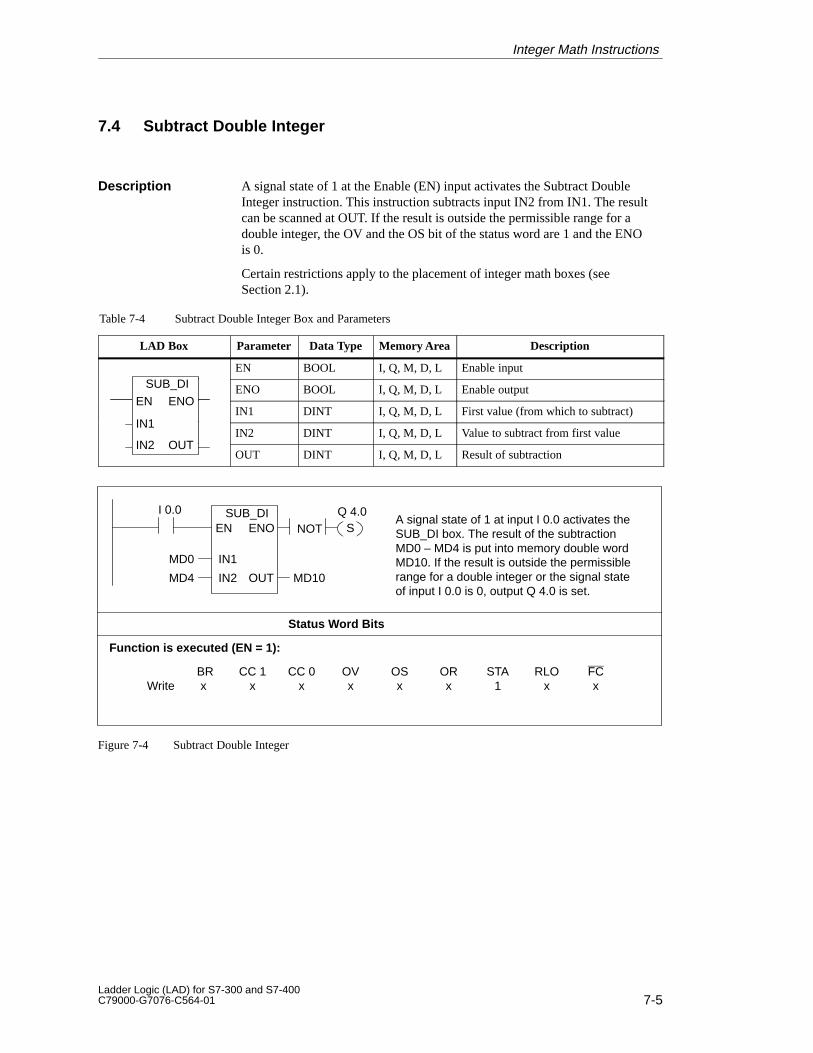
7-5Ladder Logic (LAD) for S7-300 and S7-400C79000-G7076-C564-01
7.4 Subtract Double Integer
A signal state of 1 at the Enable (EN) input activates the Subtract DoubleInteger instruction. This instruction subtracts input IN2 from IN1. The resultcan be scanned at OUT. If the result is outside the permissible range for adouble integer, the OV and the OS bit of the status word are 1 and the ENOis 0.
Certain restrictions apply to the placement of integer math boxes (seeSection 2.1).
Table 7-4 Subtract Double Integer Box and Parameters
LAD Box Parameter Data Type Memory Area Description
SUB DIEN BOOL I, Q, M, D, L Enable input
SUB_DI
EN ENOENO BOOL I, Q, M, D, L Enable output
IN1
EN ENOIN1 DINT I, Q, M, D, L First value (from which to subtract)
IN1
IN2 OUTIN2 DINT I, Q, M, D, L Value to subtract from first value
IN2 OUTOUT DINT I, Q, M, D, L Result of subtraction
Status Word Bits
BR CC 1 CC 0 OV OS OR STA RLO FCWrite x x x x x x 1 x x
I 0.0A signal state of 1 at input I 0.0 activates theSUB_DI box. The result of the subtractionMD0 – MD4 is put into memory double wordMD10. If the result is outside the permissiblerange for a double integer or the signal stateof input I 0.0 is 0, output Q 4.0 is set.
Q 4.0SUB_DI
IN2
EN ENO
MD4 MD10
IN1MD0
S
Function is executed (EN = 1):
NOT
OUT
Figure 7-4 Subtract Double Integer
Description
Integer Math Instructions

7-6Ladder Logic (LAD) for S7-300 and S7-400
C79000-G7076-C564-01
7.5 Multiply Integer
A signal state of 1 at the Enable (EN) input activates the Multiply Integerinstruction. This instruction multiplies inputs IN1 and IN2. The result is a32-bit integer that can be scanned at OUT. If the result is outside thepermissible range for a 16-bit integer, the OV and the OS bit of the statusword are 1 and the ENO is 0.
Certain restrictions apply to the placement of integer math boxes (seeSection 2.1).
Table 7-5 Multiply Integer Box and Parameters
LAD Box Parameter Data Type Memory Area Description
MUL IEN BOOL I, Q, M, D, L Enable input
MUL_I
EN ENOENO BOOL I, Q, M, D, L Enable output
IN1
EN ENOIN1 INT I, Q, M, D, L First value for multiplication
IN1
IN2 OUTIN2 INT I, Q, M, D, L Second value for multiplication
IN2 OUTOUT DINT I, Q, M, D, L Result of multiplication
Status Word Bits
BR CC 1 CC 0 OV OS OR STA RLO FCWrite x x x x x x 1 x x
I 0.0 A signal state of 1 at input I 0.0 activates theMUL_I box. The result of the multiplicationMW0 x MW2 is put into memory double wordMD10. If the result is outside the permissiblerange for a 16-bit integer or the signal stateof input I 0.0 is 0, output Q 4.0 is set.
Q 4.0MUL_I
IN2
EN ENO
MW2 MD10
IN1MW0
S
Function is executed (EN = 1):
NOT
OUT
Figure 7-5 Multiply Integer
Description
Integer Math Instructions

7-7Ladder Logic (LAD) for S7-300 and S7-400C79000-G7076-C564-01
7.6 Multiply Double Integer
A signal state of 1 at the Enable (EN) input activates the Multiply DoubleInteger instruction. This instruction multiplies inputs IN1 and IN2. The resultcan be scanned at OUT. If the result is outside the permissible range for adouble integer, the OV and the OS bit of the status word are 1 and the ENO is0.
Certain restrictions apply to the placement of integer math boxes (seeSection 2.1).
Table 7-6 Multiply Double Integer Box and Parameters
LAD Box Parameter Data Type Memory Area Description
MUL DIEN BOOL I, Q, M, D, L Enable input
MUL_DI
EN ENOENO BOOL I, Q, M, D, L Enable output
IN1
EN ENOIN1 DINT I, Q, M, D, L First value for multiplication
IN1
IN2 OUTIN2 DINT I, Q, M, D, L Second value for multiplication
IN2 OUTOUT DINT I, Q, M, D, L Result of multiplication
Status Word Bits
BR CC 1 CC 0 OV OS OR STA RLO FCWrite x x x x x x 1 x x
I 0.0A signal state of 1 at input I 0.0 activates theMUL_DI box. The result of the multiplicationMD0 x MD4 is put into memory double wordMD10. If the result is outside the permissiblerange for a double integer or the signal state ofinput I 0.0 is 0, output Q 4.0 is set.
Q 4.0MUL_DI
IN2
EN ENO
MD4 MD10
IN1MD0
S
Function is executed (EN = 1):
NOT
OUT
Figure 7-6 Multiply Double Integer
Description
Integer Math Instructions
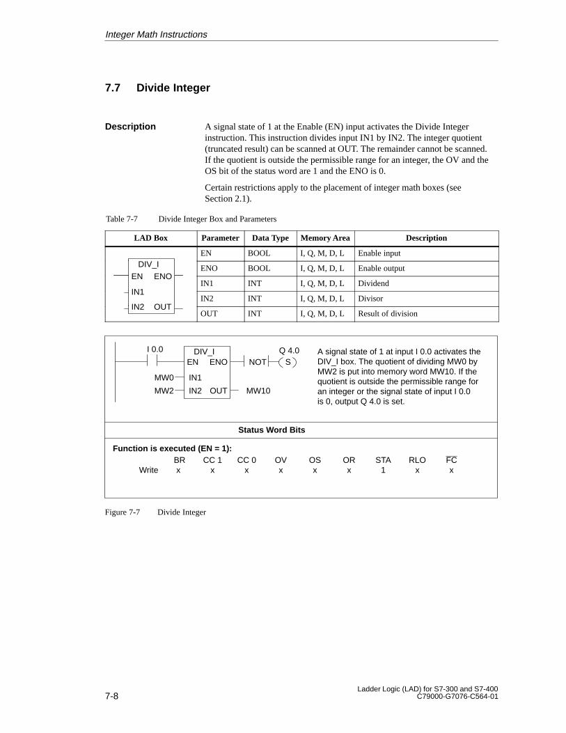
7-8Ladder Logic (LAD) for S7-300 and S7-400
C79000-G7076-C564-01
7.7 Divide Integer
A signal state of 1 at the Enable (EN) input activates the Divide Integerinstruction. This instruction divides input IN1 by IN2. The integer quotient(truncated result) can be scanned at OUT. The remainder cannot be scanned.If the quotient is outside the permissible range for an integer, the OV and theOS bit of the status word are 1 and the ENO is 0.
Certain restrictions apply to the placement of integer math boxes (seeSection 2.1).
Table 7-7 Divide Integer Box and Parameters
LAD Box Parameter Data Type Memory Area Description
DIV IEN BOOL I, Q, M, D, L Enable input
DIV_I
EN ENOENO BOOL I, Q, M, D, L Enable output
IN1
EN ENOIN1 INT I, Q, M, D, L Dividend
IN1
IN2 OUTIN2 INT I, Q, M, D, L Divisor
IN2 OUTOUT INT I, Q, M, D, L Result of division
Status Word Bits
BR CC 1 CC 0 OV OS OR STA RLO FCWrite x x x x x x 1 x x
I 0.0 A signal state of 1 at input I 0.0 activates theDIV_I box. The quotient of dividing MW0 byMW2 is put into memory word MW10. If thequotient is outside the permissible range foran integer or the signal state of input I 0.0is 0, output Q 4.0 is set.
Q 4.0DIV_I
IN2
EN ENO
MW2 MW10
IN1MW0
S
Function is executed (EN = 1):
NOT
OUT
Figure 7-7 Divide Integer
Description
Integer Math Instructions
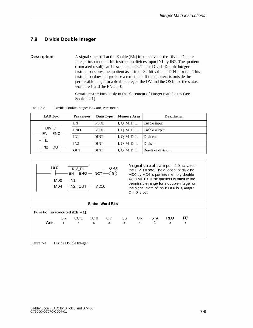
7-9Ladder Logic (LAD) for S7-300 and S7-400C79000-G7076-C564-01
7.8 Divide Double Integer
A signal state of 1 at the Enable (EN) input activates the Divide DoubleInteger instruction. This instruction divides input IN1 by IN2. The quotient(truncated result) can be scanned at OUT. The Divide Double Integerinstruction stores the quotient as a single 32-bit value in DINT format. Thisinstruction does not produce a remainder. If the quotient is outside thepermissible range for a double integer, the OV and the OS bit of the statusword are 1 and the ENO is 0.
Certain restrictions apply to the placement of integer math boxes (seeSection 2.1).
Table 7-8 Divide Double Integer Box and Parameters
LAD Box Parameter Data Type Memory Area Description
DIV DIEN BOOL I, Q, M, D, L Enable input
DIV_DI
EN ENOENO BOOL I, Q, M, D, L Enable output
IN1
EN ENOIN1 DINT I, Q, M, D, L Dividend
IN1
IN2 OUTIN2 DINT I, Q, M, D, L Divisor
IN2 OUTOUT DINT I, Q, M, D, L Result of division
Status Word Bits
BR CC 1 CC 0 OV OS OR STA RLO FCWrite x x x x x x 1 x x
I 0.0 A signal state of 1 at input I 0.0 activatesthe DIV_DI box. The quotient of dividingMD0 by MD4 is put into memory doubleword MD10. If the quotient is outside thepermissible range for a double integer orthe signal state of input I 0.0 is 0, outputQ 4.0 is set.
Q 4.0DIV_DI
IN2
EN ENO
MD4 MD10
IN1MD0
S
Function is executed (EN = 1):
NOT
OUT
Figure 7-8 Divide Double Integer
Description
Integer Math Instructions
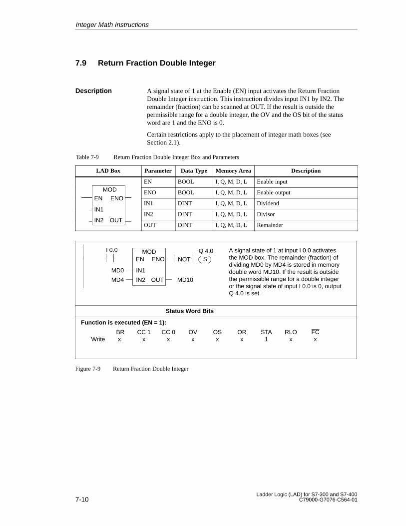
7-10Ladder Logic (LAD) for S7-300 and S7-400
C79000-G7076-C564-01
7.9 Return Fraction Double Integer
A signal state of 1 at the Enable (EN) input activates the Return FractionDouble Integer instruction. This instruction divides input IN1 by IN2. Theremainder (fraction) can be scanned at OUT. If the result is outside thepermissible range for a double integer, the OV and the OS bit of the statusword are 1 and the ENO is 0.
Certain restrictions apply to the placement of integer math boxes (seeSection 2.1).
Table 7-9 Return Fraction Double Integer Box and Parameters
LAD Box Parameter Data Type Memory Area Description
MODEN BOOL I, Q, M, D, L Enable input
MOD
EN ENOENO BOOL I, Q, M, D, L Enable output
IN1
EN ENOIN1 DINT I, Q, M, D, L Dividend
IN1
IN2 OUTIN2 DINT I, Q, M, D, L Divisor
IN2 OUTOUT DINT I, Q, M, D, L Remainder
Status Word Bits
I 0.0 A signal state of 1 at input I 0.0 activatesthe MOD box. The remainder (fraction) ofdividing MD0 by MD4 is stored in memorydouble word MD10. If the result is outsidethe permissible range for a double integeror the signal state of input I 0.0 is 0, outputQ 4.0 is set.
Q 4.0MOD
IN2
EN ENO
MD4 MD10
IN1MD0
S
Function is executed (EN = 1):
NOT
OUT
BR CC 1 CC 0 OV OS OR STA RLO FCWrite x x x x x x 1 x x
Figure 7-9 Return Fraction Double Integer
Description
Integer Math Instructions
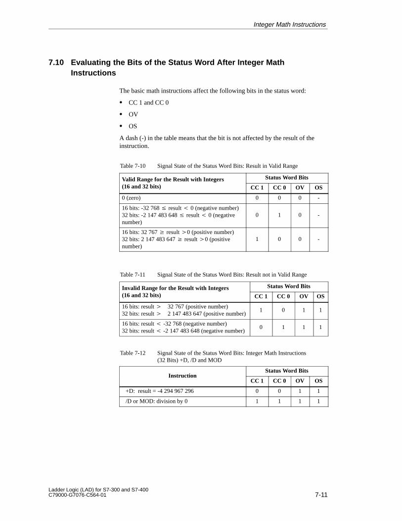
7-11Ladder Logic (LAD) for S7-300 and S7-400C79000-G7076-C564-01
7.10 Evaluating the Bits of the Status Word After Integer MathInstructions
The basic math instructions affect the following bits in the status word:
� CC 1 and CC 0
� OV
� OS
A dash (-) in the table means that the bit is not affected by the result of theinstruction.
Table 7-10 Signal State of the Status Word Bits: Result in Valid Range
Valid Range for the Result with Integers Status Word Bitsg g(16 and 32 bits) CC 1 CC 0 OV OS
0 (zero) 0 0 0 -
16 bits: -32 768 � � result � 0 (negative number)32 bits: -2 147 483 648 � � result � 0 (negativenumber)
0 1 0 -
16 bits: 32 767 � result �0 (positive number)32 bits: 2 147 483 647 � result �0 (positivenumber)
1 0 0 -
Table 7-11 Signal State of the Status Word Bits: Result not in Valid Range
Invalid Range for the Result with Integers Status Word Bitsg g(16 and 32 bits) CC 1 CC 0 OV OS
16 bits: result �� 32 767 (positive number)32 bits: result �� 2 147 483 647 (positive number)
1 0 1 1
16 bits: result � -32 768 (negative number)32 bits: result � -2 147 483 648 (negative number)
0 1 1 1
Table 7-12 Signal State of the Status Word Bits: Integer Math Instructions (32 Bits) +D, /D and MOD
InstructionStatus Word Bits
InstructionCC 1 CC 0 OV OS
+D: result = -4 294 967 296 0 0 1 1
/D or MOD: division by 0 1 1 1 1
Integer Math Instructions

7-12Ladder Logic (LAD) for S7-300 and S7-400
C79000-G7076-C564-01
Integer Math Instructions
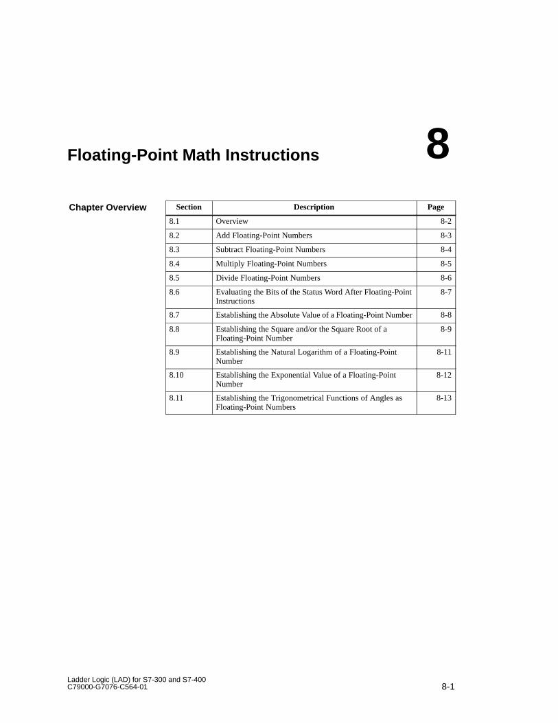
8-1Ladder Logic (LAD) for S7-300 and S7-400C79000-G7076-C564-01
Floating-Point Math Instructions
Section Description Page
8.1 Overview 8-2
8.2 Add Floating-Point Numbers 8-3
8.3 Subtract Floating-Point Numbers 8-4
8.4 Multiply Floating-Point Numbers 8-5
8.5 Divide Floating-Point Numbers 8-6
8.6 Evaluating the Bits of the Status Word After Floating-PointInstructions
8-7
8.7 Establishing the Absolute Value of a Floating-Point Number 8-8
8.8 Establishing the Square and/or the Square Root of aFloating-Point Number
8-9
8.9 Establishing the Natural Logarithm of a Floating-PointNumber
8-11
8.10 Establishing the Exponential Value of a Floating-PointNumber
8-12
8.11 Establishing the Trigonometrical Functions of Angles asFloating-Point Numbers
8-13
Chapter Overview
8
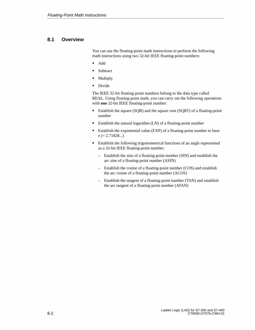
8-2Ladder Logic (LAD) for S7-300 and S7-400
C79000-G7076-C564-01
8.1 Overview
You can use the floating-point math instructions to perform the followingmath instructions using two 32-bit IEEE floating-point numbers:
� Add
� Subtract
� Multiply
� Divide
The IEEE 32-bit floating-point numbers belong to the data type calledREAL. Using floating-point math, you can carry out the following operationswith one 32-bit IEEE floating-point number:
� Establish the square (SQR) and the square root (SQRT) of a floating-pointnumber
� Establish the natural logarithm (LN) of a floating-point number
� Establish the exponential value (EXP) of a floating-point number to basee (= 2.71828...)
� Establish the following trigonometrical functions of an angle representedas a 32-bit IEEE floating-point number:
– Establish the sine of a floating-point number (SIN) and establish thearc sine of a floating-point number (ASIN)
– Establish the cosine of a floating-point number (COS) and establishthe arc cosine of a floating-point number (ACOS)
– Establish the tangent of a floating-point number (TAN) and establishthe arc tangent of a floating-point number (ATAN)
Floating-Point Math Instructions
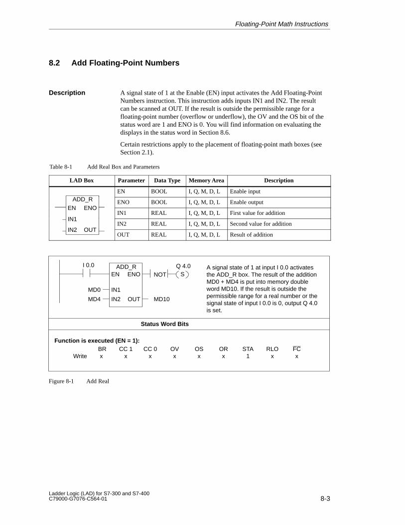
8-3Ladder Logic (LAD) for S7-300 and S7-400C79000-G7076-C564-01
8.2 Add Floating-Point Numbers
A signal state of 1 at the Enable (EN) input activates the Add Floating-PointNumbers instruction. This instruction adds inputs IN1 and IN2. The resultcan be scanned at OUT. If the result is outside the permissible range for afloating-point number (overflow or underflow), the OV and the OS bit of thestatus word are 1 and ENO is 0. You will find information on evaluating thedisplays in the status word in Section 8.6.
Certain restrictions apply to the placement of floating-point math boxes (seeSection 2.1).
Table 8-1 Add Real Box and Parameters
LAD Box Parameter Data Type Memory Area Description
ADD REN BOOL I, Q, M, D, L Enable input
ADD_R
EN ENOENO BOOL I, Q, M, D, L Enable output
IN1
EN ENOIN1 REAL I, Q, M, D, L First value for addition
IN1
IN2 OUTIN2 REAL I, Q, M, D, L Second value for addition
IN2 OUTOUT REAL I, Q, M, D, L Result of addition
Status Word Bits
BR CC 1 CC 0 OV OS OR STA RLO FCWrite x x x x x x 1 x x
I 0.0 A signal state of 1 at input I 0.0 activatesthe ADD_R box. The result of the additionMD0 + MD4 is put into memory doubleword MD10. If the result is outside thepermissible range for a real number or thesignal state of input I 0.0 is 0, output Q 4.0is set.
Q 4.0ADD_R
IN2
EN ENO
MD4 MD10
IN1MD0
S
Function is executed (EN = 1):
NOT
OUT
Figure 8-1 Add Real
Description
Floating-Point Math Instructions
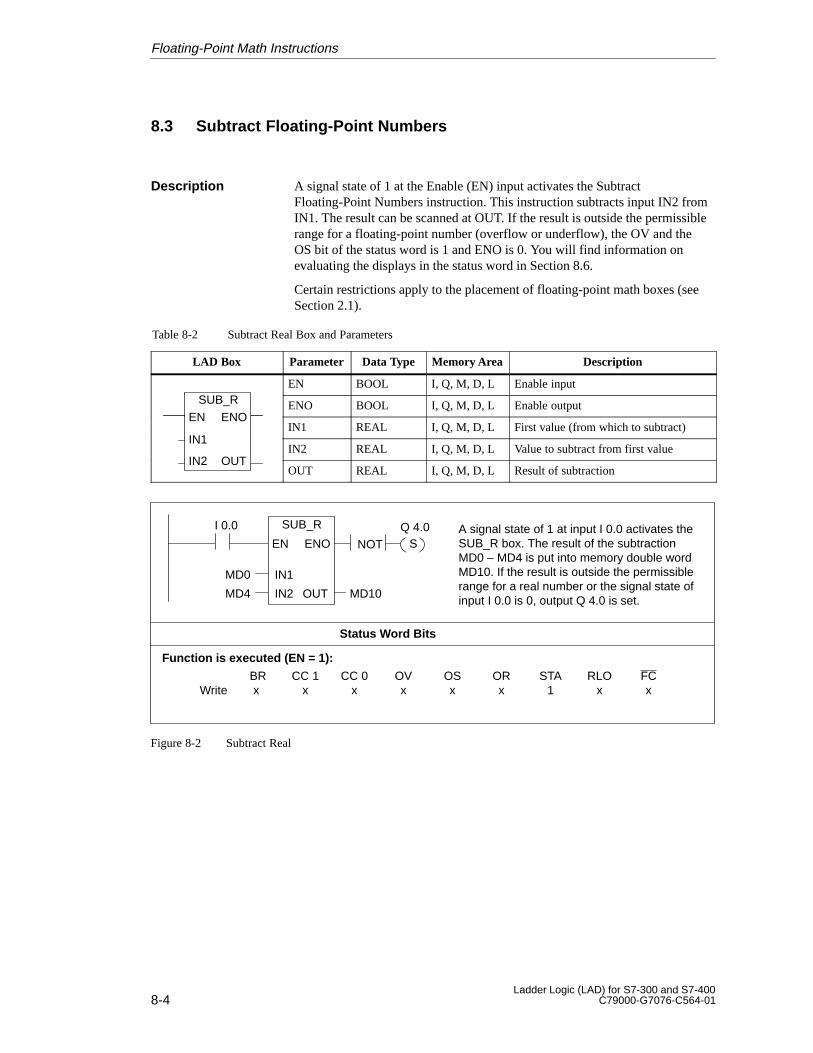
8-4Ladder Logic (LAD) for S7-300 and S7-400
C79000-G7076-C564-01
8.3 Subtract Floating-Point Numbers
A signal state of 1 at the Enable (EN) input activates the SubtractFloating-Point Numbers instruction. This instruction subtracts input IN2 fromIN1. The result can be scanned at OUT. If the result is outside the permissiblerange for a floating-point number (overflow or underflow), the OV and theOS bit of the status word is 1 and ENO is 0. You will find information onevaluating the displays in the status word in Section 8.6.
Certain restrictions apply to the placement of floating-point math boxes (seeSection 2.1).
Table 8-2 Subtract Real Box and Parameters
LAD Box Parameter Data Type Memory Area Description
SUB REN BOOL I, Q, M, D, L Enable input
SUB_R
EN ENOENO BOOL I, Q, M, D, L Enable output
IN1
EN ENOIN1 REAL I, Q, M, D, L First value (from which to subtract)
IN1
IN2 OUTIN2 REAL I, Q, M, D, L Value to subtract from first value
IN2 OUTOUT REAL I, Q, M, D, L Result of subtraction
Status Word Bits
BR CC 1 CC 0 OV OS OR STA RLO FCWrite x x x x x x 1 x x
I 0.0 A signal state of 1 at input I 0.0 activates theSUB_R box. The result of the subtractionMD0 – MD4 is put into memory double wordMD10. If the result is outside the permissiblerange for a real number or the signal state ofinput I 0.0 is 0, output Q 4.0 is set.
Q 4.0SUB_R
IN2
EN ENO
MD4 MD10
IN1MD0
S
Function is executed (EN = 1):
NOT
OUT
Figure 8-2 Subtract Real
Description
Floating-Point Math Instructions
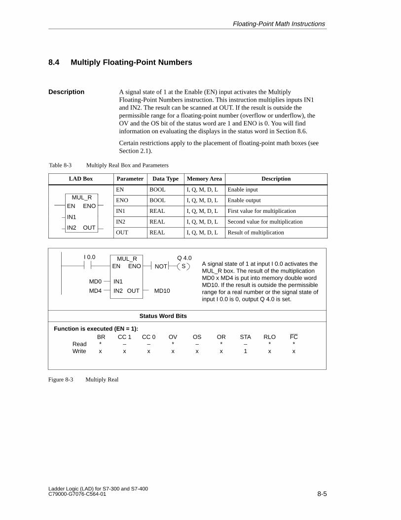
8-5Ladder Logic (LAD) for S7-300 and S7-400C79000-G7076-C564-01
8.4 Multiply Floating-Point Numbers
A signal state of 1 at the Enable (EN) input activates the MultiplyFloating-Point Numbers instruction. This instruction multiplies inputs IN1and IN2. The result can be scanned at OUT. If the result is outside thepermissible range for a floating-point number (overflow or underflow), theOV and the OS bit of the status word are 1 and ENO is 0. You will findinformation on evaluating the displays in the status word in Section 8.6.
Certain restrictions apply to the placement of floating-point math boxes (seeSection 2.1).
Table 8-3 Multiply Real Box and Parameters
LAD Box Parameter Data Type Memory Area Description
MUL REN BOOL I, Q, M, D, L Enable input
MUL_R
EN ENOENO BOOL I, Q, M, D, L Enable output
IN1
EN ENOIN1 REAL I, Q, M, D, L First value for multiplication
IN1
IN2 OUTIN2 REAL I, Q, M, D, L Second value for multiplication
IN2 OUTOUT REAL I, Q, M, D, L Result of multiplication
Status Word Bits
BR CC 1 CC 0 OV OS OR STA RLO FCRead * – – * – * – * *Write x x x x x x 1 x x
I 0.0A signal state of 1 at input I 0.0 activates theMUL_R box. The result of the multiplicationMD0 x MD4 is put into memory double wordMD10. If the result is outside the permissiblerange for a real number or the signal state ofinput I 0.0 is 0, output Q 4.0 is set.
Q 4.0MUL_R
IN2
EN ENO
MD4 MD10
IN1MD0
S
Function is executed (EN = 1):
NOT
OUT
Figure 8-3 Multiply Real
Description
Floating-Point Math Instructions
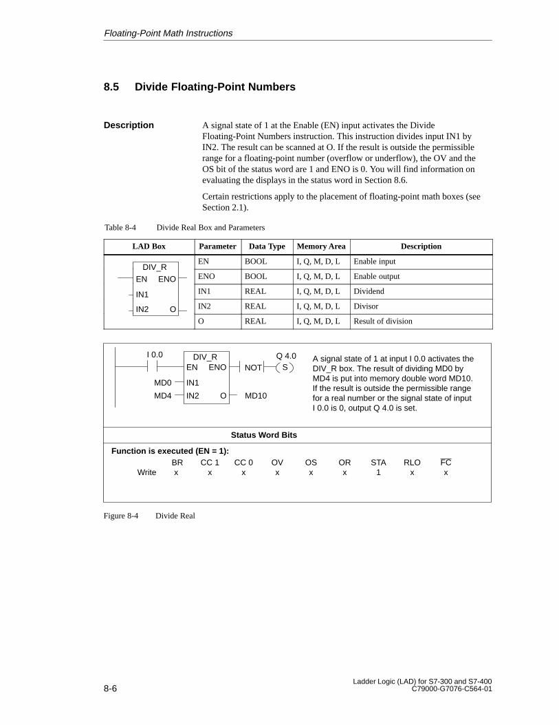
8-6Ladder Logic (LAD) for S7-300 and S7-400
C79000-G7076-C564-01
8.5 Divide Floating-Point Numbers
A signal state of 1 at the Enable (EN) input activates the DivideFloating-Point Numbers instruction. This instruction divides input IN1 byIN2. The result can be scanned at O. If the result is outside the permissiblerange for a floating-point number (overflow or underflow), the OV and theOS bit of the status word are 1 and ENO is 0. You will find information onevaluating the displays in the status word in Section 8.6.
Certain restrictions apply to the placement of floating-point math boxes (seeSection 2.1).
Table 8-4 Divide Real Box and Parameters
LAD Box Parameter Data Type Memory Area Description
DIV REN BOOL I, Q, M, D, L Enable input
DIV_R
EN ENO ENO BOOL I, Q, M, D, L Enable output
IN1 IN1 REAL I, Q, M, D, L DividendIN1
IN2 O IN2 REAL I, Q, M, D, L DivisorOO REAL I, Q, M, D, L Result of division
Status Word Bits
BR CC 1 CC 0 OV OS OR STA RLO FCWrite x x x x x x 1 x x
I 0.0 A signal state of 1 at input I 0.0 activates theDIV_R box. The result of dividing MD0 byMD4 is put into memory double word MD10.If the result is outside the permissible rangefor a real number or the signal state of inputI 0.0 is 0, output Q 4.0 is set.
Q 4.0DIV_R
IN2
EN ENO
MD4 MD10
IN1MD0
S
Function is executed (EN = 1):
NOT
O
Figure 8-4 Divide Real
Description
Floating-Point Math Instructions

8-7Ladder Logic (LAD) for S7-300 and S7-400C79000-G7076-C564-01
8.6 Evaluating the Bits of the Status Word After Floating-PointInstructions
The math instructions affect the following bits in the status word:
� CC 1 and CC 0
� OV
� OS
A hyphen (–) entered in a bit column of the table means that the bit inquestion is not affected by the result of the integer math instruction.
Table 8-5 Signal State of Status Word Bits for Floating-Point Math Result that is in Valid Range
Valid Range for a Floating-Point Result (32 Bits)Bits of Status Word
Valid Range for a Floating-Point Result (32 Bits)CC 1 CC 0 OV OS
+0, -0 (zero) 0 0 0 –
-3.402823E+38 � Result � -1.175494E-38 (negative number)
0 1 0 –
+1.175494E–38 � Result �� 3.402823E+38(positive number)
1 0 0 –
Table 8-6 Signal State of Status Word Bits for Floating-Point Math Result that is not in Valid Range
Range Not Valid for a Floating-Point Result Bits of Status Wordg g(32 Bits) CC 1 CC 0 OV OS
-1.175494E-38 �� Result � -1.401298E-45(negative number) Underflow
0 0 1 1
+1.401298E-45 �� Result � +1.175494E-38(positive number) Underflow
0 0 1 1
Result �� -3.402823E+38(negative number) Overflow
0 1 1 1
Result �� -3.402823E+38(positive number) Overflow
1 0 1 1
Result < -3.402823E+38 or Result > +3.402823E+38
no floating-point number
1 1 1 1
Description
Floating-Point Math Instructions
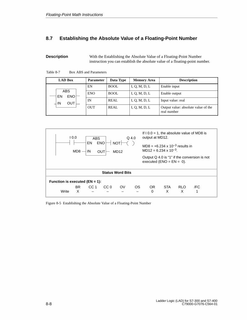
8-8Ladder Logic (LAD) for S7-300 and S7-400
C79000-G7076-C564-01
8.7 Establishing the Absolute Value of a Floating-Point Number
With the Establishing the Absolute Value of a Floating-Point Numberinstruction you can establish the absolute value of a floating-point number.
Table 8-7 Box ABS and Parameters
LAD Box Parameter Data Type Memory Area Description
ABSEN BOOL I, Q, M, D, L Enable input
ABS
EN ENOENO BOOL I, Q, M, D, L Enable output
EN
IN OUT
ENOIN REAL I, Q, M, D, L Input value: real
IN OUTOUT REAL I, Q, M, D, L Output value: absolute value of the
real number
Status Word Bits
BR CC 1 CC 0 OV OS OR STA RLO /FCWrite X – – – – 0 X X 1
I 0.0If I 0.0 = 1, the absolute value of MD8 isoutput at MD12.
MD8 = +6.234 x 10⁻³ results in MD12 = 6.234 x 10⁻³.
Output Q 4.0 is “1” if the conversion is notexecuted (ENO = EN = 0).
Q 4.0ABS
OUT
EN ENO
MD12
Function is executed (EN = 1):
NOT
INMD8
Figure 8-5 Establishing the Absolute Value of a Floating-Point Number
Description
Floating-Point Math Instructions
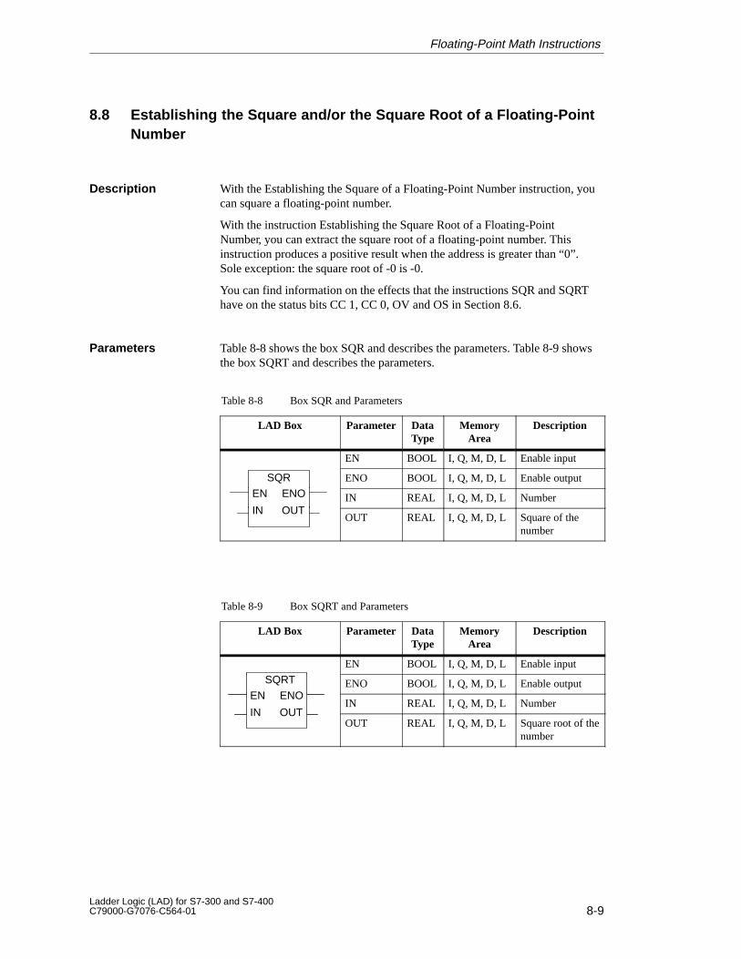
8-9Ladder Logic (LAD) for S7-300 and S7-400C79000-G7076-C564-01
8.8 Establishing the Square and/or the Square Root of a Floating-PointNumber
With the Establishing the Square of a Floating-Point Number instruction, youcan square a floating-point number.
With the instruction Establishing the Square Root of a Floating-PointNumber, you can extract the square root of a floating-point number. Thisinstruction produces a positive result when the address is greater than “0”.Sole exception: the square root of -0 is -0.
You can find information on the effects that the instructions SQR and SQRThave on the status bits CC 1, CC 0, OV and OS in Section 8.6.
Table 8-8 shows the box SQR and describes the parameters. Table 8-9 showsthe box SQRT and describes the parameters.
Table 8-8 Box SQR and Parameters
LAD Box Parameter DataType
MemoryArea
Description
EN BOOL I, Q, M, D, L Enable input
SQR
EN ENOENO BOOL I, Q, M, D, L Enable output
EN
IN OUT
ENO IN REAL I, Q, M, D, L NumberIN OUT
OUT REAL I, Q, M, D, L Square of thenumber
Table 8-9 Box SQRT and Parameters
LAD Box Parameter DataType
MemoryArea
Description
SQ
EN BOOL I, Q, M, D, L Enable input
SQRT
EN ENOENO BOOL I, Q, M, D, L Enable output
EN
IN OUT
ENOIN REAL I, Q, M, D, L Number
IN OUTOUT REAL I, Q, M, D, L Square root of the
number
Description
Parameters
Floating-Point Math Instructions
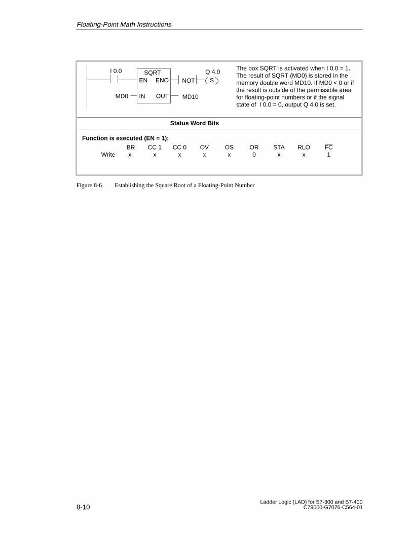
8-10Ladder Logic (LAD) for S7-300 and S7-400
C79000-G7076-C564-01
Status Word Bits
BR CC 1 CC 0 OV OS OR STA RLO FCWrite x x x x x 0 x x 1
Function is executed (EN = 1):
I 0.0 Q 4.0SQRT
OUT
EN ENO
MD10INMD0
SNOT
The box SQRT is activated when I 0.0 = 1.The result of SQRT (MD0) is stored in thememory double word MD10. If MD0 < 0 or ifthe result is outside of the permissible areafor floating-point numbers or if the signalstate of I 0.0 = 0, output Q 4.0 is set.
Figure 8-6 Establishing the Square Root of a Floating-Point Number
Floating-Point Math Instructions
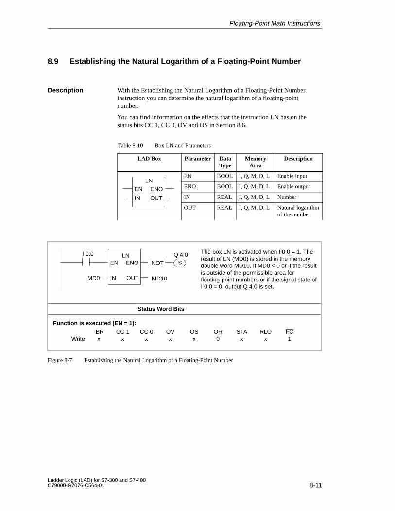
8-11Ladder Logic (LAD) for S7-300 and S7-400C79000-G7076-C564-01
8.9 Establishing the Natural Logarithm of a Floating-Point Number
With the Establishing the Natural Logarithm of a Floating-Point Numberinstruction you can determine the natural logarithm of a floating-pointnumber.
You can find information on the effects that the instruction LN has on thestatus bits CC 1, CC 0, OV and OS in Section 8.6.
Table 8-10 Box LN and Parameters
LAD Box Parameter DataType
MemoryArea
Description
LNEN BOOL I, Q, M, D, L Enable input
LN
EN ENO ENO BOOL I, Q, M, D, L Enable outputEN
IN OUT
ENOIN REAL I, Q, M, D, L Number
OUT REAL I, Q, M, D, L Natural logarithmof the number
Status Word Bits
BR CC 1 CC 0 OV OS OR STA RLO FCWrite x x x x x 0 x x 1
Function is executed (EN = 1):
I 0.0 Q 4.0LN
OUT
EN ENO
MD10INMD0
SNOT
The box LN is activated when I 0.0 = 1. Theresult of LN (MD0) is stored in the memorydouble word MD10. If MD0 < 0 or if the resultis outside of the permissible area forfloating-point numbers or if the signal state ofI 0.0 = 0, output Q 4.0 is set.
Figure 8-7 Establishing the Natural Logarithm of a Floating-Point Number
Description
Floating-Point Math Instructions
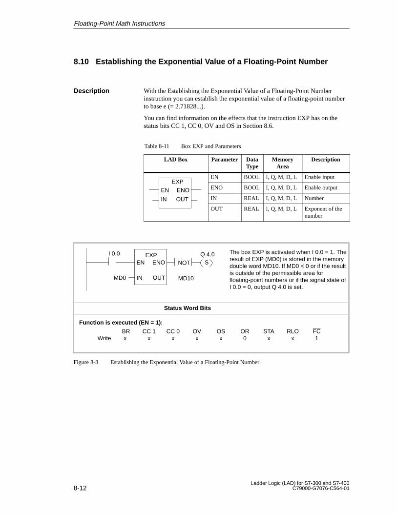
8-12Ladder Logic (LAD) for S7-300 and S7-400
C79000-G7076-C564-01
8.10 Establishing the Exponential Value of a Floating-Point Number
With the Establishing the Exponential Value of a Floating-Point Numberinstruction you can establish the exponential value of a floating-point numberto base e (= 2.71828...).
You can find information on the effects that the instruction EXP has on thestatus bits CC 1, CC 0, OV and OS in Section 8.6.
Table 8-11 Box EXP and Parameters
LAD Box Parameter DataType
MemoryArea
Description
EXPEN BOOL I, Q, M, D, L Enable input
EXP
EN ENO ENO BOOL I, Q, M, D, L Enable outputEN
IN OUT
ENOIN REAL I, Q, M, D, L Number
OUT REAL I, Q, M, D, L Exponent of thenumber
Status Word Bits
BR CC 1 CC 0 OV OS OR STA RLO FCWrite x x x x x 0 x x 1
Function is executed (EN = 1):
I 0.0 Q 4.0EXP
OUT
EN ENO
MD10INMD0
SNOT
The box EXP is activated when I 0.0 = 1. Theresult of EXP (MD0) is stored in the memorydouble word MD10. If MD0 < 0 or if the resultis outside of the permissible area forfloating-point numbers or if the signal state ofI 0.0 = 0, output Q 4.0 is set.
Figure 8-8 Establishing the Exponential Value of a Floating-Point Number
Description
Floating-Point Math Instructions
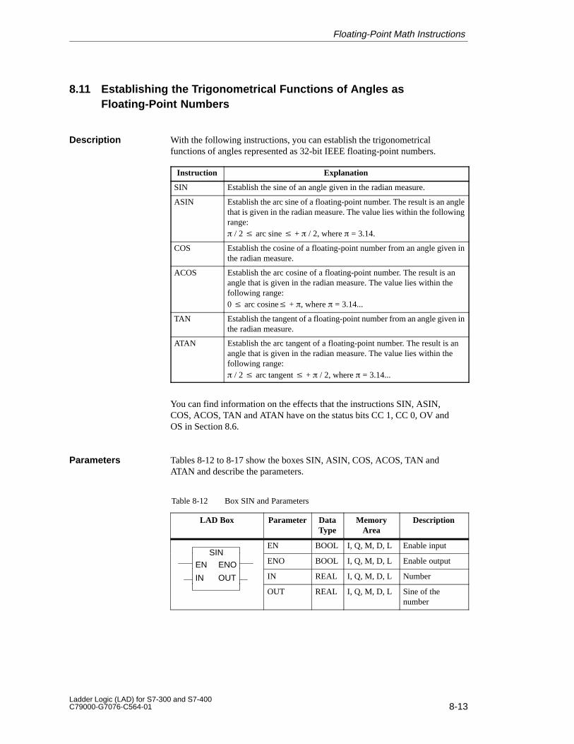
8-13Ladder Logic (LAD) for S7-300 and S7-400C79000-G7076-C564-01
8.11 Establishing the Trigonometrical Functions of Angles asFloating-Point Numbers
With the following instructions, you can establish the trigonometricalfunctions of angles represented as 32-bit IEEE floating-point numbers.
Instruction Explanation
SIN Establish the sine of an angle given in the radian measure.
ASIN Establish the arc sine of a floating-point number. The result is an anglethat is given in the radian measure. The value lies within the followingrange:��/ 2 � arc sine � + � / 2, where � = 3.14.
COS Establish the cosine of a floating-point number from an angle given inthe radian measure.
ACOS Establish the arc cosine of a floating-point number. The result is anangle that is given in the radian measure. The value lies within thefollowing range:0 � arc cosine� + �, where � = 3.14...
TAN Establish the tangent of a floating-point number from an angle given inthe radian measure.
ATAN Establish the arc tangent of a floating-point number. The result is anangle that is given in the radian measure. The value lies within thefollowing range:��/ 2 � arc tangent � + � / 2, where � = 3.14...
You can find information on the effects that the instructions SIN, ASIN,COS, ACOS, TAN and ATAN have on the status bits CC 1, CC 0, OV andOS in Section 8.6.
Tables 8-12 to 8-17 show the boxes SIN, ASIN, COS, ACOS, TAN andATAN and describe the parameters.
Table 8-12 Box SIN and Parameters
LAD Box Parameter DataType
MemoryArea
Description
SINEN BOOL I, Q, M, D, L Enable input
SIN
EN ENO ENO BOOL I, Q, M, D, L Enable outputEN
IN OUT
ENOIN REAL I, Q, M, D, L Number
OUT REAL I, Q, M, D, L Sine of thenumber
Description
Parameters
Floating-Point Math Instructions
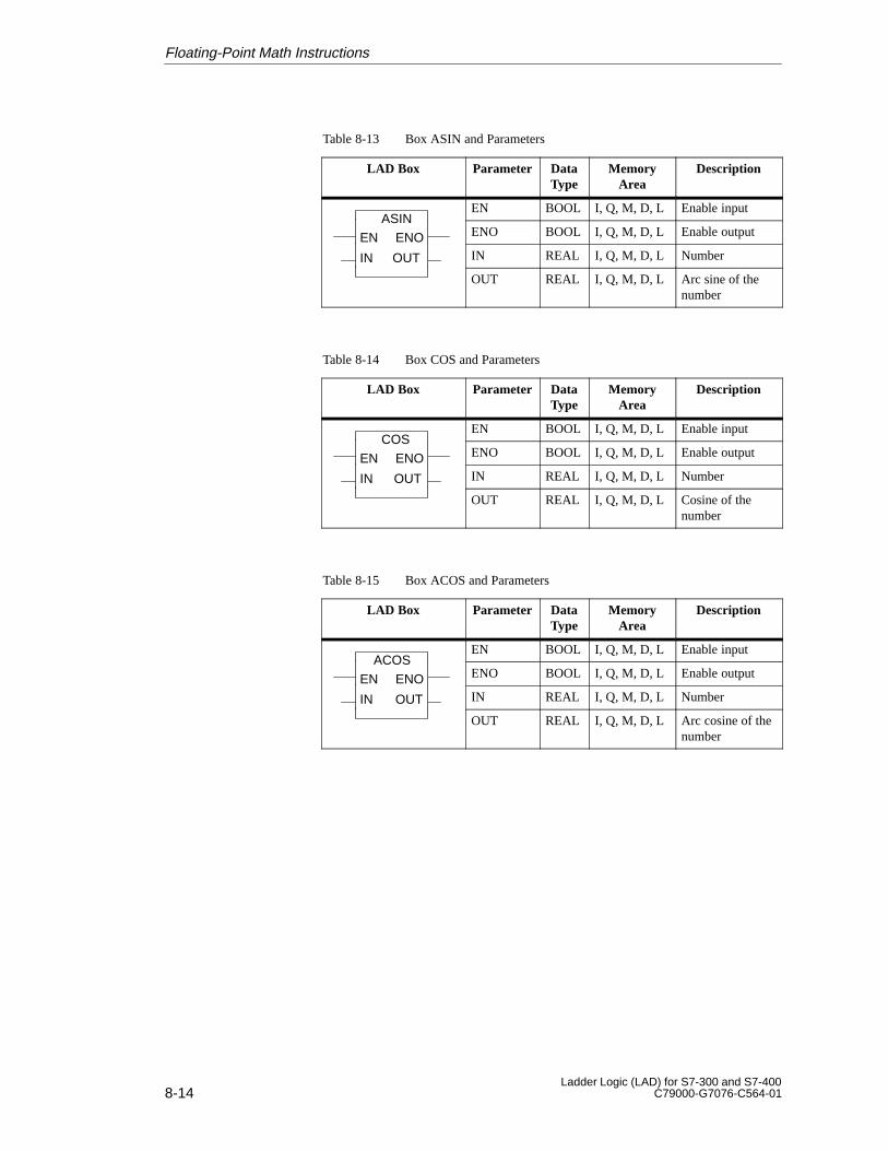
8-14Ladder Logic (LAD) for S7-300 and S7-400
C79000-G7076-C564-01
Table 8-13 Box ASIN and Parameters
LAD Box Parameter DataType
MemoryArea
Description
ASINEN BOOL I, Q, M, D, L Enable input
ASIN
EN ENO ENO BOOL I, Q, M, D, L Enable outputEN
IN OUT
ENOIN REAL I, Q, M, D, L Number
OUT REAL I, Q, M, D, L Arc sine of thenumber
Table 8-14 Box COS and Parameters
LAD Box Parameter DataType
MemoryArea
Description
COSEN BOOL I, Q, M, D, L Enable input
COS
EN ENO ENO BOOL I, Q, M, D, L Enable outputEN
IN OUT
ENOIN REAL I, Q, M, D, L Number
OUT REAL I, Q, M, D, L Cosine of thenumber
Table 8-15 Box ACOS and Parameters
LAD Box Parameter DataType
MemoryArea
Description
ACOSEN BOOL I, Q, M, D, L Enable input
ACOS
EN ENO ENO BOOL I, Q, M, D, L Enable outputEN
IN OUT
ENOIN REAL I, Q, M, D, L Number
OUT REAL I, Q, M, D, L Arc cosine of thenumber
Floating-Point Math Instructions
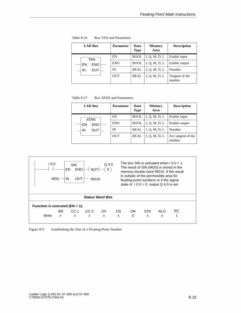
8-15Ladder Logic (LAD) for S7-300 and S7-400C79000-G7076-C564-01
Table 8-16 Box TAN and Parameters
LAD Box Parameter DataType
MemoryArea
Description
TANEN BOOL I, Q, M, D, L Enable input
TAN
EN ENO ENO BOOL I, Q, M, D, L Enable outputEN
IN OUT
ENOIN REAL I, Q, M, D, L Number
OUT REAL I, Q, M, D, L Tangent of thenumber
Table 8-17 Box ATAN and Parameters
LAD Box Parameter DataType
MemoryArea
Description
ATANEN BOOL I, Q, M, D, L Enable input
ATAN
EN ENO ENO BOOL I, Q, M, D, L Enable outputEN
IN OUT
ENOIN REAL I, Q, M, D, L Number
OUT REAL I, Q, M, D, L Arc tangent of thenumber
Status Word Bits
BR CC 1 CC 0 OV OS OR STA RLO FCWrite x x x x x 0 x x 1
Function is executed (EN = 1):
I 0.0 Q 4.0SIN
OUT
EN ENO
MD10INMD0
SNOT
The box SIN is activated when I 0.0 = 1.The result of SIN (MD0) is stored in thememory double word MD10. If the resultis outside of the permissible area forfloating-point numbers or if the signalstate of I 0.0 = 0, output Q 4.0 is set.
Figure 8-9 Establishing the Sine of a Floating-Point Number
Floating-Point Math Instructions

8-16Ladder Logic (LAD) for S7-300 and S7-400
C79000-G7076-C564-01
Floating-Point Math Instructions
9-1Ladder Logic (LAD) for S7-300 and S7-400C79000-G7076-C564-01
Comparison Instructions
Section Description Page
9.1 Compare Integer 9-2
9.2 Compare Double Integer 9-3
9.3 Compare Floating-Point Numbers 9-5
Chapter Overview
9
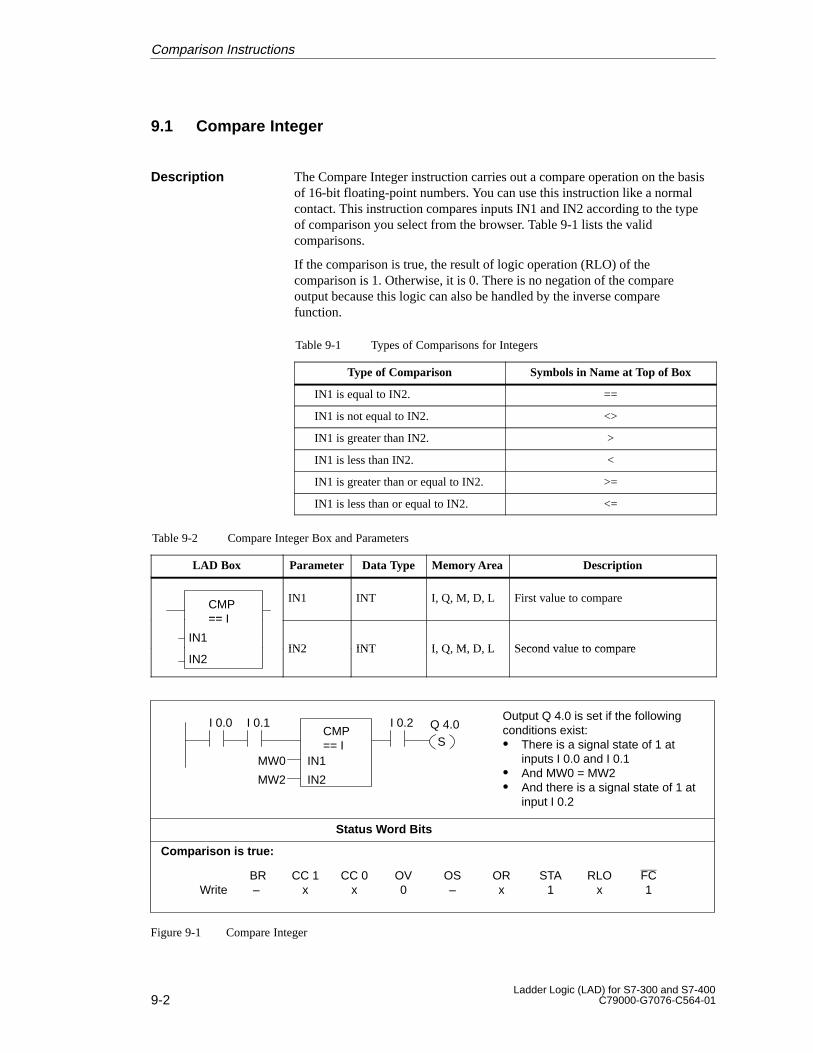
9-2Ladder Logic (LAD) for S7-300 and S7-400
C79000-G7076-C564-01
9.1 Compare Integer
The Compare Integer instruction carries out a compare operation on the basisof 16-bit floating-point numbers. You can use this instruction like a normalcontact. This instruction compares inputs IN1 and IN2 according to the typeof comparison you select from the browser. Table 9-1 lists the validcomparisons.
If the comparison is true, the result of logic operation (RLO) of thecomparison is 1. Otherwise, it is 0. There is no negation of the compareoutput because this logic can also be handled by the inverse comparefunction.
Table 9-1 Types of Comparisons for Integers
Type of Comparison Symbols in Name at Top of Box
IN1 is equal to IN2. ==
IN1 is not equal to IN2. <>
IN1 is greater than IN2. >
IN1 is less than IN2. <
IN1 is greater than or equal to IN2. >=
IN1 is less than or equal to IN2. <=
Table 9-2 Compare Integer Box and Parameters
LAD Box Parameter Data Type Memory Area Description
CMP== I
IN1 INT I, Q, M, D, L First value to compare
== I
IN1IN2 INT I Q M D L Second value to compare
IN2IN2 INT I, Q, M, D, L Second value to compare
Status Word Bits
BR CC 1 CC 0 OV OS OR STA RLO FCWrite – x x 0 – x 1 x 1
I 0.1 Output Q 4.0 is set if the followingconditions exist:� There is a signal state of 1 at
inputs I 0.0 and I 0.1� And MW0 = MW2� And there is a signal state of 1 at
input I 0.2
Q 4.0CMP== I
IN2MW2
IN1MW0
I 0.0 I 0.2
S
Comparison is true:
Figure 9-1 Compare Integer
Description
Comparison Instructions
9-3Ladder Logic (LAD) for S7-300 and S7-400C79000-G7076-C564-01
9.2 Compare Double Integer
The Compare Double Integer instruction carries out a compare operation onthe basis of 32-bit floating-point numbers. You can use this instruction like anormal contact. This instruction compares inputs IN1 and IN2 according tothe type of comparison you select from the browser. Table 9-3 lists the validcomparisons.
If the comparison is true, the result of logic operation (RLO) of the functionis 1. Otherwise it is 0. There is no negation of the compare output, becausethis logic can also be handled by the inverse compare function.
Table 9-3 Types of Comparisons for Double Integers
Type of Comparison Symbols in Name at Top of Box
IN1 is equal to IN2. ==
IN1 is not equal to IN2. <>
IN1 is greater than IN2. >
IN1 is less than IN2. <
IN1 is greater than or equal to IN2. >=
IN1 is less than or equal to IN2. <=
Table 9-4 Compare Double Integer Box and Parameters (Example: not equal)
LAD Box Parameter Data Type Memory Area Description
CMP<> D
IN1 DINT I, Q, M, D, L First value to compare
IN1
<> D
IN2 DINT I Q M D L Second value to compareIN2
IN2 DINT I, Q, M, D, L Second value to compare
Description
Comparison Instructions
9-4Ladder Logic (LAD) for S7-300 and S7-400
C79000-G7076-C564-01
Status Word Bits
BR CC 1 CC 0 OV OS OR STA RLO FCWrite – x x 0 – x 1 x 1
I 0.1
Output Q 4.0 is set if the followingconditions exist:� There is a signal state of 1 at
inputs I 0.0 and at I 0.1� And MD0 = MD4� And there is a signal state of 1 at
input I 0.2
Q 4.0CMP== D
IN2MD4
IN1MD0
I 0.0 I 0.2
S
Comparison is true:
Figure 9-2 Compare Double Integer
Comparison Instructions
9-5Ladder Logic (LAD) for S7-300 and S7-400C79000-G7076-C564-01
9.3 Compare Floating-Point Numbers
The Compare Floating-Point Numbers instruction triggers a comparisonoperation. You can use this instruction like a normal contact. This instructioncompares inputs IN1 and IN2 according to the type of comparison you selectfrom the browser. Table 9-5 lists the valid comparisons.
If the comparison is true, the result of logic operation (RLO) of the functionis 1. Otherwise it is 0. There is no negation of the compare output, becausethis logic can also be handled by the inverse compare function.
Table 9-5 Types of Comparisons for Floating-Point Numbers
Type of Comparison Symbols in Name at Top of Box
IN1 is equal to IN2. ==
IN1 is not equal to IN2. <>
IN1 is greater than IN2. >
IN1 is less than IN2. <
IN1 is greater than or equal to IN2. >=
IN1 is less than or equal to IN2. <=
Table 9-6 Compare Floating-Point Numbers: Box and Parameters (Example: less than)
LAD Box Parameter Data Type Memory Area Description
CMP< R
IN1 REAL I, Q, M, D, L First value to compare
IN1
< R
IN2 REAL I Q M D L Second value to compareIN2
IN2 REAL I, Q, M, D, L Second value to compare
Status Word Bits
BR CC 1 CC 0 OV OS OR STA RLO FCWrite – x x x x x 1 x 1
I 0.1
Output Q 4.0 is set if the followingconditions exist:� There is a signal state of 1 at
inputs I 0.0 and I 0.1� And MD0 = MD4� And there is a signal state of 1 at
input I 0.2
Q 4.0CMP== R
IN2MD4
IN1MD0
I 0.0 I 0.2
S
Comparison is true:
Figure 9-3 Compare Floating-Point Numbers
Description
Comparison Instructions

9-6Ladder Logic (LAD) for S7-300 and S7-400
C79000-G7076-C564-01
Comparison Instructions
10-1Ladder Logic (LAD) for S7-300 and S7-400C79000-G7076-C564-01
Move and Conversion Instructions
Section Description Page
10.1 Assign a Value 10-2
10.2 BCD to Integer 10-4
10.3 Integer to BCD 10-5
10.4 Integer to Double Integer 10-6
10.5 BCD to Double Integer 10-7
10.6 Double Integer to BCD 10-8
10.7 Double Integer to Floating-Point Number 10-9
10.8 Ones Complement Integer 10-10
10.9 Ones Complement Double Integer 10-11
10.10 Twos Complement Integer 10-12
10.11 Twos Complement Double Integer 10-13
10.12 Negate Floating-Point Number 10-14
10.13 Round to Double Integer 10-15
10.14 Truncate Double Integer Part 10-16
10.15 Ceiling 10-17
10.16 Floor 10-18
Chapter Overview
10
10-2Ladder Logic (LAD) for S7-300 and S7-400
C79000-G7076-C564-01
10.1 Assign a Value
The Assign a Value instruction enables you to pre-assign a variable with aspecific value.
The value specified at the IN input is copied to the address specified at theOUT output. ENO has the same signal state as EN.
With the MOVE box, the Assign a Value instruction can copy all data typesthat are 8, 16, or 32 bits in length. User-defined data types such as arrays orstructures have to be copied with the Direct Word Move integrated systemfunction (see the Reference Manual /235/).
The Assign a Value instruction is affected by the Master Control Relay(MCR). For more information on how the MCR functions, see Section 16.5.
Certain restrictions apply to the placement of the Assign a Value box (seeSection 2.1).
Table 10-1 Assign a Value Box and Parameters
LAD Box Parameter Data Type Memory Area Description
EN BOOL I, Q, M, D, L Enable input
MOVEENO BOOL I, Q, M, D, L Enable output
MOVE
EN ENOIN
All data types thatare 8, 16, and 32bits in length
I, Q, M, D, Lor constant
Source value
IN OUTOUT
All data types thatare 8, 16, and 32bits in length
I, Q, M, D, L Destination address
I 0.0The instruction is executed if the signalstate of input I 0.0 is 1. The content ofmemory word MW10 is copied to dataword 12 of the open DB.
Output Q 4.0 is 1 if the operation isexecuted.
Q 4.0MOVE
IN OUT
EN ENO
MW10 DBW12
Status Word Bits
BR CC 1 CC 0 OV OS OR STA RLO FCWrite 1 – – – – – 1 1 x
Function is executed (EN = 1):
Figure 10-1 Assign a Value
Description
Move and Conversion Instructions

10-3Ladder Logic (LAD) for S7-300 and S7-400C79000-G7076-C564-01
For information on integrated system functions that act as move instructionswhich can pre-assign a specific value to a variable or which can copyvariables of varying types, see the Reference Manual /235/.
Pre-Assigning aSpecific Value to aVariable
Move and Conversion Instructions
10-4Ladder Logic (LAD) for S7-300 and S7-400
C79000-G7076-C564-01
10.2 BCD to Integer
The BCD to Integer conversion instruction reads the contents specified in theinput parameter IN as a three-digit number in binary coded decimal format(BCD, � 999) and converts this number to an integer value. The outputparameter OUT provides the result.
ENO and EN always have the same signal state.
If a place of a BCD number is in the invalid range of 10 to 15, a BCDF erroroccurs during an attempted conversion.
� The CPU goes into the STOP mode. “BCD Conversion Error” is enteredin the diagnostic buffer with event ID number 2521.
� If OB121 is programmed, it is called. For more information onprogramming OB121, see the Reference Manual /235/.
Certain restrictions apply to the placement of the BCD to Integer conversionbox (see Section 2.1).
Table 10-2 BCD to Integer Conversion Box and Parameters
LAD Box Parameter Data Type Memory Area Description
BCD IEN BOOL I, Q, M, D, L Enable input
BCD_I
EN ENOENO BOOL I, Q, M, D, L Enable output
EN
IN OUT
ENOIN WORD I, Q, M, D, L Number in BCD format
OUT INT I, Q, M, D, L Integer value of BCD number
Status Word Bits
BR CC 1 CC 0 OV OS OR STA RLO FCWrite 1 – – – – 0 1 1 x
I 0.0If the signal state of input I 0.0 is 1, theconversion is executed. The contents ofmemory word MW10 is read as athree-digit number in BCD format andconverted to an integer. The result isstored in memory word MW12. If theconversion is not executed, the signalstate of output Q 4.0 is 1 (ENO = EN).
Q 4.0BCD_I
EN ENO
MW12INMW10
NOT
Function is executed (EN = 1):
OUT
Figure 10-2 BCD to Integer
Description
Move and Conversion Instructions

10-5Ladder Logic (LAD) for S7-300 and S7-400C79000-G7076-C564-01
10.3 Integer to BCD
The Integer to BCD conversion instruction reads the contents specified in theinput parameter IN as an integer value and converts this value to a three-digitnumber in binary coded decimal format (BCD, � 999). The outputparameter OUT provides the result. If an overflow occurs, ENO is 0.
Certain restrictions apply to the placement of the Integer to BCD conversionbox (see Section 2.1).
Table 10-3 Integer to BCD Conversion Box and Parameters
LAD Box Parameter Data Type Memory Area Description
I BCDEN BOOL I, Q, M, D, L Enable input
I_BCD
EN ENO ENO BOOL I, Q, M, D, L Enable output
IN OUT IN INT I, Q, M, D, L Integer number
OUT WORD I, Q, M, D, L Result in BCD format
Status Word Bits
BR CC 1 CC 0 OV OS OR STA RLO FCWrite 1 – – x x 0 1 x x
I 0.0 If the signal state of input I 0.0 is 1, theconversion is executed. The contents ofmemory word MW10 is read as aninteger and converted to a three-digitnumber in BCD format. The result isstored in memory word MW12. If anoverflow occurred, the signal state ofoutput Q 4.0 is 1. If the signal state atinput EN is 0 (that is, if the conversion isnot executed), the signal state of outputQ 4.0 is also 1.
Q 4.0I_BCD
IN
EN ENO
MW10 MW12
Function is executed (EN = 1):
NOT
OUT
Figure 10-3 Integer to BCD
Description
Move and Conversion Instructions
10-6Ladder Logic (LAD) for S7-300 and S7-400
C79000-G7076-C564-01
10.4 Integer to Double Integer
The Integer to Double Integer conversion instruction reads the contentsspecified in the input parameter IN as an integer and converts the integer to adouble integer. The output parameter OUT provides the result. ENO and ENalways have the same signal state.
Certain restrictions apply to the placement of the Integer to Double Integerconversion box (see Section 2.1).
Table 10-4 Integer to Double Integer Conversion Box and Parameters
LAD Box Parameter Data Type Memory Area Description
I DIEN BOOL I, Q, M, D, L Enable input
I_DI
EN ENO ENO BOOL I, Q, M, D, L Enable output
IN OUT IN INT I, Q, M, D, L Value to convert
OUT DINT I, Q, M, D, L Result
Status Word Bits
I 0.0 If the signal state of input I 0.0 is 1, theconversion is executed. The contents ofmemory word MW10 is read as an integerand converted to a double integer. The resultis stored in memory double word MD12. Ifthe conversion is not executed, the signalstate of output Q 4.0 is 1 (ENO = EN).
Q 4.0I_DI
EN ENO
MD12INMW10
NOT
BR CC 1 CC 0 OV OS OR STA RLO FCWrite 1 – – – – 0 1 1 x
Function is executed (EN = 1):
OUT
Figure 10-4 Integer To Double Integer
Description
Move and Conversion Instructions
10-7Ladder Logic (LAD) for S7-300 and S7-400C79000-G7076-C564-01
10.5 BCD to Double Integer
The BCD to Double Integer conversion instruction reads the contentsspecified in the input parameter IN as a seven-digit number in binary codeddecimal format (BCD, � 9,999,999) and converts this number to a doubleinteger value. The output parameter OUT provides the result.
ENO and EN always have the same signal state.
If a place of a BCD number is in the invalid range of 10 to 15, a BCDF erroroccurs during an attempted conversion.
� The CPU goes into the STOP mode. “BCD Conversion Error” is enteredin the diagnostic buffer with event ID number 2521.
� If OB121 is programmed, it is called. For more information onprogramming OB121, see the Reference Manual /235/.
Certain restrictions apply to the placement of the BCD to Double Integerconversion box (see Section 2.1).
Table 10-5 BCD to Double Integer Conversion Box and Parameters
LAD Box Parameter Data Type Memory Area Description
BCD DIEN BOOL I, Q, M, D, L Enable input
BCD_DI
EN ENO ENO BOOL I, Q, M, D, L Enable output
IN OUT IN DWORD I, Q, M, D, L Number in BCD format
OUT DINT I, Q, M, D, L Double integer value of BCD number
Status Word Bits
I 0.0If the signal state of input I 0.0 is 1, theconversion is executed. The contents ofmemory double word MD8 is read as aseven-digit number in BCD format andconverted to a double integer. The result isstored in memory double word MD12. If theconversion is not executed, the signal stateof output Q 4.0 is 1 (ENO = EN).
Q 4.0BCD_DI
EN ENO
MD12INMD8
NOT
BR CC 1 CC 0 OV OS OR STA RLO FCWrite 1 – – – – 0 1 1 x
Function is executed (EN = 1):
OUT
Figure 10-5 BCD to Double Integer
Description
Move and Conversion Instructions
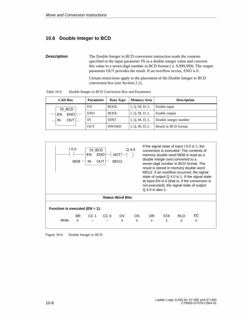
10-8Ladder Logic (LAD) for S7-300 and S7-400
C79000-G7076-C564-01
10.6 Double Integer to BCD
The Double Integer to BCD conversion instruction reads the contentsspecified in the input parameter IN as a double integer value and convertsthis value to a seven-digit number in BCD format (� 9,999,999). The outputparameter OUT provides the result. If an overflow occurs, ENO is 0.
Certain restrictions apply to the placement of the Double Integer to BCDconversion box (see Section 2.1).
Table 10-6 Double Integer to BCD Conversion Box and Parameters
LAD Box Parameter Data Type Memory Area Description
DI BCDEN BOOL I, Q, M, D, L Enable input
DI_BCD
EN ENO ENO BOOL I, Q, M, D, L Enable output
IN OUT IN DINT I, Q, M, D, L Double integer number
OUT DWORD I, Q, M, D, L Result in BCD format
Status Word Bits
BR CC 1 CC 0 OV OS OR STA RLO FCWrite x – – x x x 1 x x
I 0.0If the signal state of input I 0.0 is 1, theconversion is executed. The contents ofmemory double word MD8 is read as adouble integer and converted to aseven-digit number in BCD format. Theresult is stored in memory double wordMD12. If an overflow occurred, the signalstate of output Q 4.0 is 1. If the signal stateat input EN is 0 (that is, if the conversion isnot executed), the signal state of outputQ 4.0 is also 1.
Q 4.0DI_BCD
IN
EN ENO
MD8 MD12
Function is executed (EN = 1):
NOT
OUT
Figure 10-6 Double Integer to BCD
Description
Move and Conversion Instructions
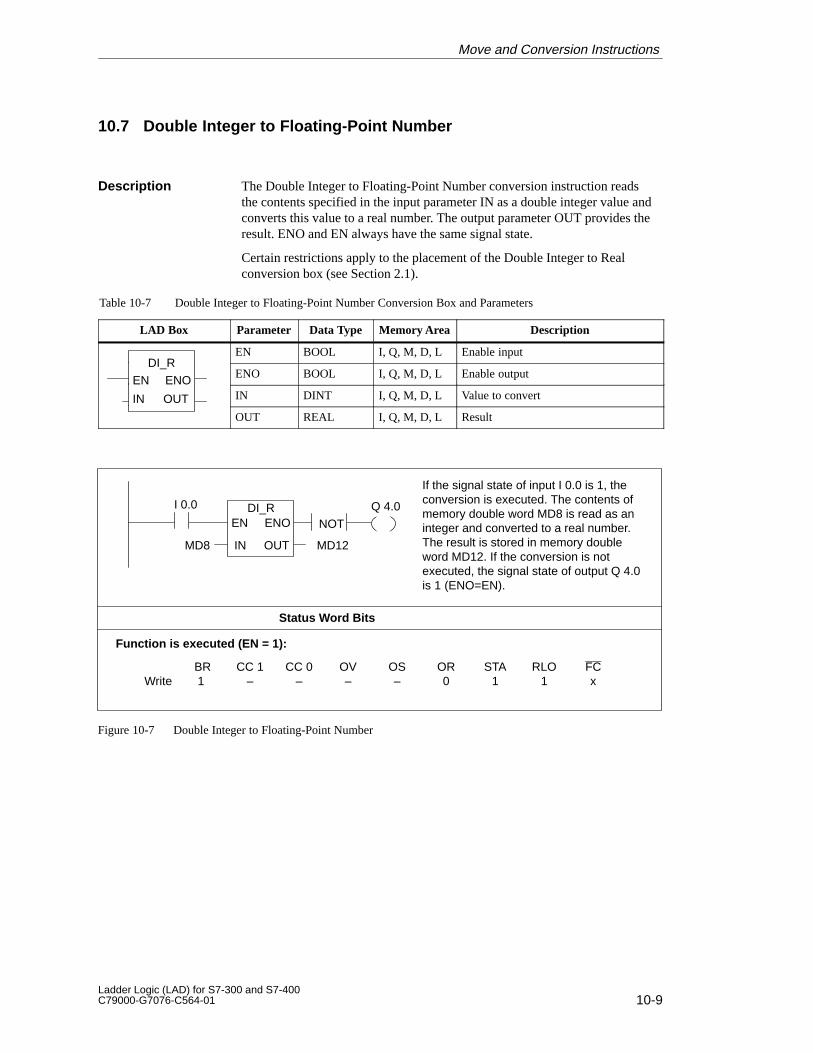
10-9Ladder Logic (LAD) for S7-300 and S7-400C79000-G7076-C564-01
10.7 Double Integer to Floating-Point Number
The Double Integer to Floating-Point Number conversion instruction readsthe contents specified in the input parameter IN as a double integer value andconverts this value to a real number. The output parameter OUT provides theresult. ENO and EN always have the same signal state.
Certain restrictions apply to the placement of the Double Integer to Realconversion box (see Section 2.1).
Table 10-7 Double Integer to Floating-Point Number Conversion Box and Parameters
LAD Box Parameter Data Type Memory Area Description
DI REN BOOL I, Q, M, D, L Enable input
DI_R
EN ENO ENO BOOL I, Q, M, D, L Enable outputEN
IN
ENO
OUT IN DINT I, Q, M, D, L Value to convert
OUT REAL I, Q, M, D, L Result
Status Word Bits
I 0.0
If the signal state of input I 0.0 is 1, theconversion is executed. The contents ofmemory double word MD8 is read as aninteger and converted to a real number.The result is stored in memory doubleword MD12. If the conversion is notexecuted, the signal state of output Q 4.0is 1 (ENO=EN).
Q 4.0DI_R
IN
EN ENO
MD8 MD12
NOT
BR CC 1 CC 0 OV OS OR STA RLO FCWrite 1 – – – – 0 1 1 x
Function is executed (EN = 1):
OUT
Figure 10-7 Double Integer to Floating-Point Number
Description
Move and Conversion Instructions
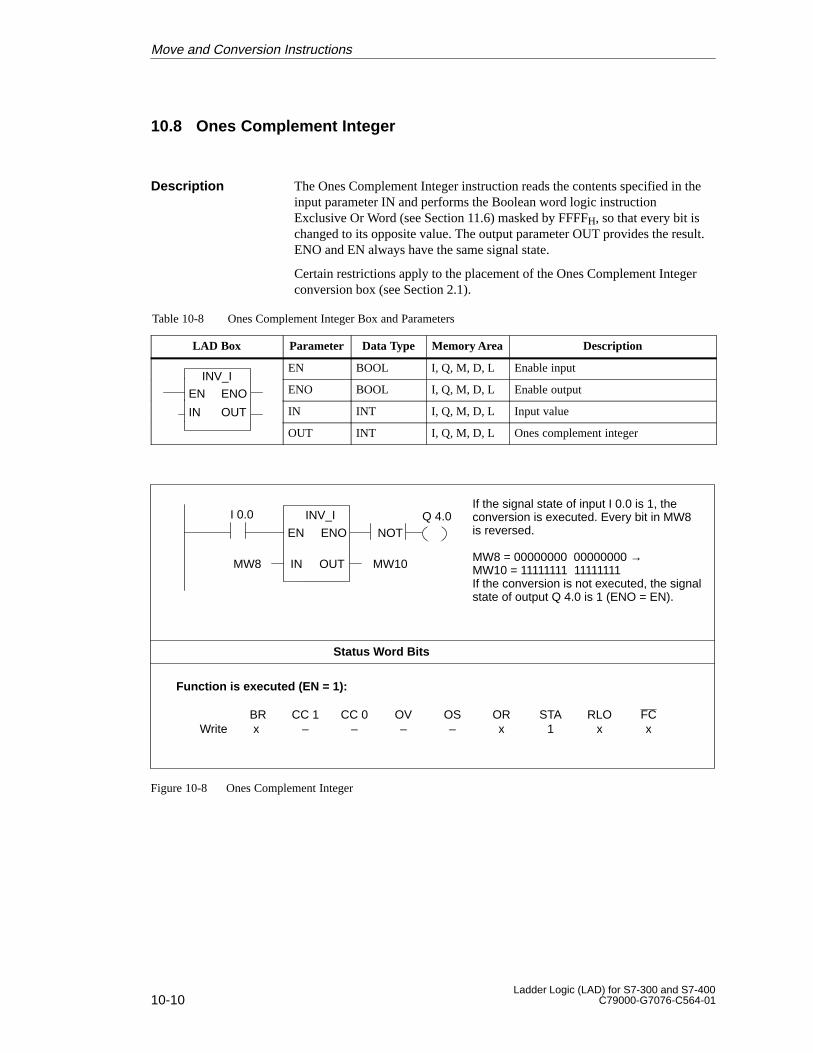
10-10Ladder Logic (LAD) for S7-300 and S7-400
C79000-G7076-C564-01
10.8 Ones Complement Integer
The Ones Complement Integer instruction reads the contents specified in theinput parameter IN and performs the Boolean word logic instructionExclusive Or Word (see Section 11.6) masked by FFFFH, so that every bit ischanged to its opposite value. The output parameter OUT provides the result.ENO and EN always have the same signal state.
Certain restrictions apply to the placement of the Ones Complement Integerconversion box (see Section 2.1).
Table 10-8 Ones Complement Integer Box and Parameters
LAD Box Parameter Data Type Memory Area Description
INV IEN BOOL I, Q, M, D, L Enable input
INV_I
EN ENO ENO BOOL I, Q, M, D, L Enable output
IN OUT IN INT I, Q, M, D, L Input value
OUT INT I, Q, M, D, L Ones complement integer
Status Word Bits
BR CC 1 CC 0 OV OS OR STA RLO FCWrite x – – – – x 1 x x
I 0.0If the signal state of input I 0.0 is 1, theconversion is executed. Every bit in MW8is reversed.
MW8 = 00000000 00000000 →MW10 = 11111111 11111111If the conversion is not executed, the signalstate of output Q 4.0 is 1 (ENO = EN).
Q 4.0INV_I
EN ENO
MW10INMW8
NOT
OUT
Function is executed (EN = 1):
Figure 10-8 Ones Complement Integer
Description
Move and Conversion Instructions
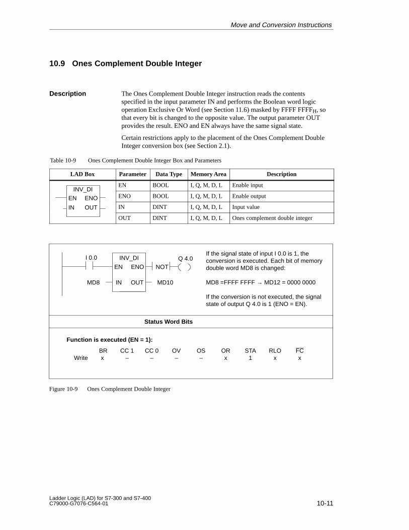
10-11Ladder Logic (LAD) for S7-300 and S7-400C79000-G7076-C564-01
10.9 Ones Complement Double Integer
The Ones Complement Double Integer instruction reads the contentsspecified in the input parameter IN and performs the Boolean word logicoperation Exclusive Or Word (see Section 11.6) masked by FFFF FFFFH, sothat every bit is changed to the opposite value. The output parameter OUTprovides the result. ENO and EN always have the same signal state.
Certain restrictions apply to the placement of the Ones Complement DoubleInteger conversion box (see Section 2.1).
Table 10-9 Ones Complement Double Integer Box and Parameters
LAD Box Parameter Data Type Memory Area Description
INV DIEN BOOL I, Q, M, D, L Enable input
INV_DI
EN ENO ENO BOOL I, Q, M, D, L Enable output
IN OUT IN DINT I, Q, M, D, L Input value
OUT DINT I, Q, M, D, L Ones complement double integer
Status Word Bits
BR CC 1 CC 0 OV OS OR STA RLO FCWrite x – – – – x 1 x x
I 0.0If the signal state of input I 0.0 is 1, theconversion is executed. Each bit of memorydouble word MD8 is changed:
MD8 =FFFF FFFF → MD12 = 0000 0000
If the conversion is not executed, the signalstate of output Q 4.0 is 1 (ENO = EN).
Q 4.0INV_DI
EN ENO
MD10INMD8
NOT
OUT
Function is executed (EN = 1):
Figure 10-9 Ones Complement Double Integer
Description
Move and Conversion Instructions
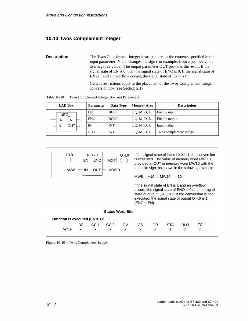
10-12Ladder Logic (LAD) for S7-300 and S7-400
C79000-G7076-C564-01
10.10 Twos Complement Integer
The Twos Complement Integer instruction reads the contents specified in theinput parameter IN and changes the sign (for example, from a positive valueto a negative value). The output parameter OUT provides the result. If thesignal state of EN is 0, then the signal state of ENO is 0. If the signal state ofEN is 1 and an overflow occurs, the signal state of ENO is 0.
Certain restrictions apply to the placement of the Twos Complement Integerconversion box (see Section 2.1).
Table 10-10 Twos Complement Integer Box and Parameters
LAD Box Parameter Data Type Memory Area Description
NEG IEN BOOL I, Q, M, D, L Enable input
NEG_I
EN ENO ENO BOOL I, Q, M, D, L Enable output
IN OUT IN INT I, Q, M, D, L Input value
OUT INT I, Q, M, D, L Twos complement integer
Status Word Bits
I 0.0 If the signal state of input I 0.0 is 1, the conversionis executed. The value of memory word MW8 isprovided at OUT in memory word MW10 with theopposite sign, as shown in the following example:
MW8 = +10 → MW10 = – 10
If the signal state of EN is 1 and an overflowoccurs, the signal state of ENO is 0 and the signalstate of output Q 4.0 is 1. If the conversion is notexecuted, the signal state of output Q 4.0 is 1(ENO = EN).
Q 4.0NEG_I
EN ENO
MW10INMW8
BR CC 1 CC 0 OV OS OR STA RLO FCWrite x x x x x x 1 x x
Function is executed (EN = 1):
NOT
OUT
Figure 10-10 Twos Complement Integer
Description
Move and Conversion Instructions
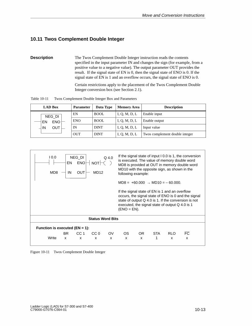
10-13Ladder Logic (LAD) for S7-300 and S7-400C79000-G7076-C564-01
10.11 Twos Complement Double Integer
The Twos Complement Double Integer instruction reads the contentsspecified in the input parameter IN and changes the sign (for example, from apositive value to a negative value). The output parameter OUT provides theresult. If the signal state of EN is 0, then the signal state of ENO is 0. If thesignal state of EN is 1 and an overflow occurs, the signal state of ENO is 0.
Certain restrictions apply to the placement of the Twos Complement DoubleInteger conversion box (see Section 2.1).
Table 10-11 Twos Complement Double Integer Box and Parameters
LAD Box Parameter Data Type Memory Area Description
NEG DIEN BOOL I, Q, M, D, L Enable input
NEG_DI
EN ENO ENO BOOL I, Q, M, D, L Enable output
IN OUT IN DINT I, Q, M, D, L Input value
OUT DINT I, Q, M, D, L Twos complement double integer
Status Word Bits
I 0.0 If the signal state of input I 0.0 is 1, the conversionis executed. The value of memory double wordMD8 is provided at OUT in memory double wordMD10 with the opposite sign, as shown in thefollowing example:
MD8 = +60.000 → MD10 = – 60.000.
If the signal state of EN is 1 and an overflowoccurs, the signal state of ENO is 0 and the signalstate of output Q 4.0 is 1. If the conversion is notexecuted, the signal state of output Q 4.0 is 1(ENO = EN).
Q 4.0NEG_DI
EN ENO
MD12INMD8
BR CC 1 CC 0 OV OS OR STA RLO FCWrite x x x x x x 1 x x
Function is executed (EN = 1):
NOT
OUT
Figure 10-11 Twos Complement Double Integer
Description
Move and Conversion Instructions
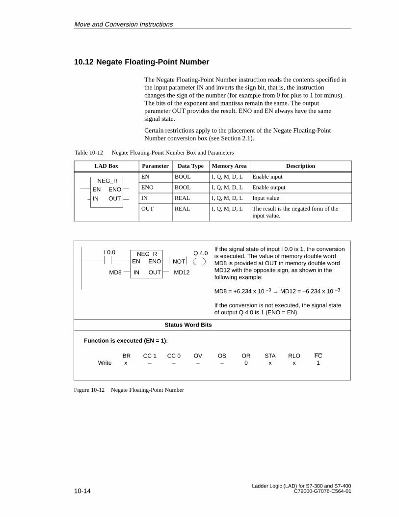
10-14Ladder Logic (LAD) for S7-300 and S7-400
C79000-G7076-C564-01
10.12 Negate Floating-Point Number
The Negate Floating-Point Number instruction reads the contents specified inthe input parameter IN and inverts the sign bit, that is, the instructionchanges the sign of the number (for example from 0 for plus to 1 for minus).The bits of the exponent and mantissa remain the same. The outputparameter OUT provides the result. ENO and EN always have the samesignal state.
Certain restrictions apply to the placement of the Negate Floating-PointNumber conversion box (see Section 2.1).
Table 10-12 Negate Floating-Point Number Box and Parameters
LAD Box Parameter Data Type Memory Area Description
NEG REN BOOL I, Q, M, D, L Enable input
NEG_R
EN ENO ENO BOOL I, Q, M, D, L Enable output
IN OUT IN REAL I, Q, M, D, L Input value
OUT REAL I, Q, M, D, L The result is the negated form of theinput value.
Status Word Bits
I 0.0 If the signal state of input I 0.0 is 1, the conversionis executed. The value of memory double wordMD8 is provided at OUT in memory double wordMD12 with the opposite sign, as shown in thefollowing example:
MD8 = +6.234 x 10 –3 → MD12 = –6.234 x 10 –3
If the conversion is not executed, the signal stateof output Q 4.0 is 1 (ENO = EN).
Q 4.0NEG_R
IN
EN ENO
MD8 MD12
BR CC 1 CC 0 OV OS OR STA RLO FCWrite x – – – – 0 x x 1
NOT
OUT
Function is executed (EN = 1):
Figure 10-12 Negate Floating-Point Number
Move and Conversion Instructions
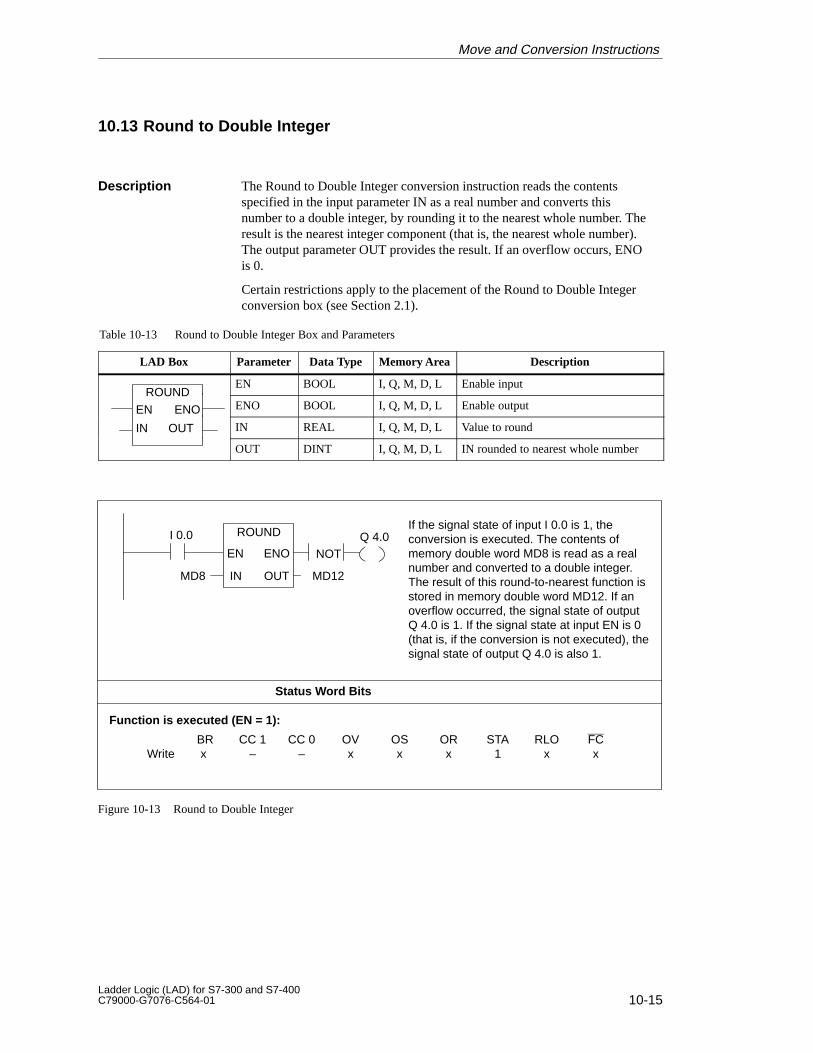
10-15Ladder Logic (LAD) for S7-300 and S7-400C79000-G7076-C564-01
10.13 Round to Double Integer
The Round to Double Integer conversion instruction reads the contentsspecified in the input parameter IN as a real number and converts thisnumber to a double integer, by rounding it to the nearest whole number. Theresult is the nearest integer component (that is, the nearest whole number).The output parameter OUT provides the result. If an overflow occurs, ENOis 0.
Certain restrictions apply to the placement of the Round to Double Integerconversion box (see Section 2.1).
Table 10-13 Round to Double Integer Box and Parameters
LAD Box Parameter Data Type Memory Area Description
ROUNDEN BOOL I, Q, M, D, L Enable input
ROUND
EN ENO ENO BOOL I, Q, M, D, L Enable output
IN OUT IN REAL I, Q, M, D, L Value to round
OUT DINT I, Q, M, D, L IN rounded to nearest whole number
Status Word Bits
BR CC 1 CC 0 OV OS OR STA RLO FCWrite x – – x x x 1 x x
I 0.0If the signal state of input I 0.0 is 1, theconversion is executed. The contents ofmemory double word MD8 is read as a realnumber and converted to a double integer.The result of this round-to-nearest function isstored in memory double word MD12. If anoverflow occurred, the signal state of outputQ 4.0 is 1. If the signal state at input EN is 0(that is, if the conversion is not executed), thesignal state of output Q 4.0 is also 1.
Q 4.0ROUND
IN
EN ENO
MD8 MD12
Function is executed (EN = 1):
NOT
OUT
Figure 10-13 Round to Double Integer
Description
Move and Conversion Instructions

10-16Ladder Logic (LAD) for S7-300 and S7-400
C79000-G7076-C564-01
10.14 Truncate Double Integer Part
The Truncate Double Integer Part conversion instruction reads the contentsspecified in the input parameter IN as a real number and converts thisnumber to a double integer, by rounding it to the nearest lower or equalwhole number. The result is the integer component of the specified realnumber (that is, the whole number part of the real number). The outputparameter OUT provides the result. If an overflow occurs, ENO is 0.
Certain restrictions apply to the placement of the Truncate Double IntegerPart conversion box (see Section 2.1).
Table 10-14 Truncate Double Integer Part Box and Parameters
LAD Box Parameter Data Type Memory Area Description
TRUNCEN BOOL I, Q, M, D, L Enable input
TRUNC
EN ENO ENO BOOL I, Q, M, D, L Enable output
IN OUT IN REAL I, Q, M, D, L Value to roundIN OUTOUT DINT I, Q, M, D, L Whole number part of IN value
Status Word Bits
BR CC 1 CC 0 OV OS OR STA RLO FCWrite x – – x x x 1 x x
I 0.0If the signal state of input I 0.0 is 1, theconversion is executed. The contents ofmemory double word MD8 is read as a realnumber and converted to a double integer.The integer component is the result and isstored in memory double word MD12. If anoverflow occurred, the signal state of outputQ 4.0 is 1. If the signal state at input EN is 0(that is, if the conversion is not executed),the signal state of output Q 4.0 is also 1.
Q 4.0TRUNC
IN
EN ENO
MD8 MD12
Function is executed (EN = 1):
NOT
OUT
Figure 10-14 Truncate Double Integer Part
Description
Move and Conversion Instructions
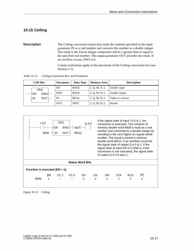
10-17Ladder Logic (LAD) for S7-300 and S7-400C79000-G7076-C564-01
10.15 Ceiling
The Ceiling conversion instruction reads the contents specified in the inputparameter IN as a real number and converts this number to a double integer.The result is the lowest integer component which is greater than or equal tothe specified real number. The output parameter OUT provides the result. Ifan overflow occurs, ENO is 0.
Certain restrictions apply to the placement of the Ceiling conversion box (seeSection 2.1).
Table 10-15 Ceiling Conversion Box and Parameters
LAD Box Parameter Data Type Memory Area Description
CEILEN BOOL I, Q, M, D, L Enable input
CEIL
EN ENO ENO BOOL I, Q, M, D, L Enable output
IN OUT IN REAL I, Q, M, D, L Value to convert
OUT DINT I, Q, M, D, L Result
Status Word Bits
BR CC 1 CC 0 OV OS OR STA RLO FCWrite x – – x x x 1 x x
I 0.0If the signal state of input I 0.0 is 1, theconversion is executed. The contents ofmemory double word MD8 is read as a realnumber and converted to a double integer byrounding to the next higher (or equal) wholenumber. The result is stored in memorydouble word MD12. If an overflow occurred,the signal state of output Q 4.0 is 1. If thesignal state at input EN is 0 (that is, if theconversion is not executed), the signal stateof output Q 4.0 is also 1.
Q 4.0CEIL
IN
EN ENO
MD8 MD12
Function is executed (EN = 1):
NOT
OUT
Figure 10-15 Ceiling
Description
Move and Conversion Instructions
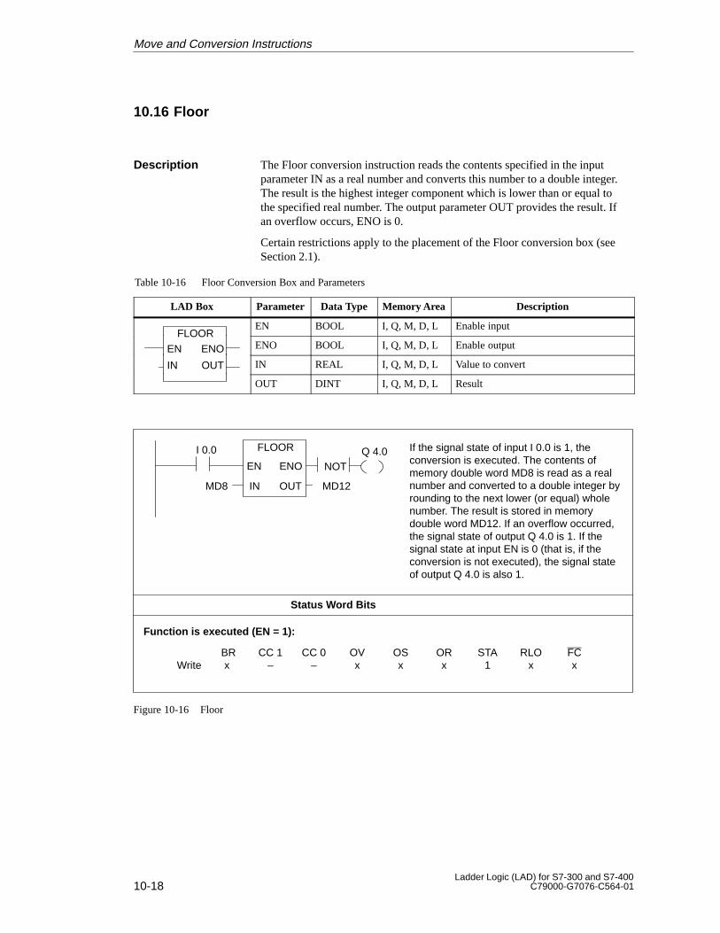
10-18Ladder Logic (LAD) for S7-300 and S7-400
C79000-G7076-C564-01
10.16 Floor
The Floor conversion instruction reads the contents specified in the inputparameter IN as a real number and converts this number to a double integer.The result is the highest integer component which is lower than or equal tothe specified real number. The output parameter OUT provides the result. Ifan overflow occurs, ENO is 0.
Certain restrictions apply to the placement of the Floor conversion box (seeSection 2.1).
Table 10-16 Floor Conversion Box and Parameters
LAD Box Parameter Data Type Memory Area Description
FLOOREN BOOL I, Q, M, D, L Enable input
FLOOR
EN ENO ENO BOOL I, Q, M, D, L Enable output
IN OUT IN REAL I, Q, M, D, L Value to convert
OUT DINT I, Q, M, D, L Result
Status Word Bits
BR CC 1 CC 0 OV OS OR STA RLO FCWrite x – – x x x 1 x x
I 0.0 If the signal state of input I 0.0 is 1, theconversion is executed. The contents ofmemory double word MD8 is read as a realnumber and converted to a double integer byrounding to the next lower (or equal) wholenumber. The result is stored in memorydouble word MD12. If an overflow occurred,the signal state of output Q 4.0 is 1. If thesignal state at input EN is 0 (that is, if theconversion is not executed), the signal stateof output Q 4.0 is also 1.
Q 4.0FLOOR
IN
EN ENO
MD8 MD12
Function is executed (EN = 1):
NOT
OUT
Figure 10-16 Floor
Description
Move and Conversion Instructions
11-1Ladder Logic (LAD) for S7-300 and S7-400C79000-G7076-C564-01
Word Logic Instructions
Section Description Page
11.1 Overview 11-2
11.2 WAnd Word 11-3
11.3 WAnd Double Word 11-4
11.4 WOr Word 11-5
11.5 WOr Double Word 11-6
11.6 WXOr Word 11-7
11.7 WXOr Double Word 11-8
Chapter Overview
11

11-2Ladder Logic (LAD) for S7-300 and S7-400
C79000-G7076-C564-01
11.1 Overview
Word logic instructions compare pairs of words (16 bits) and double words(32 bits) bit by bit, according to Boolean logic. The following instructionsare available for performing word logic operations:
� (Word) And Word: Combines two words bit by bit, according to the Andtruth table.
� (Word) And Double Word: Combines two double words bit by bit,according to the And truth table.
� (Word) Or Word: Combines two words bit by bit, according to the Ortruth table.
� (Word) Or Double Word: Combines two double words bit by bit,according to the Or truth table.
� (Word) Exclusive Or Word: Combines two words bit by bit, according tothe Exclusive Or truth table.
� (Word) Exclusive Or Double Word: Combines two double words bit bybit, according to the Exclusive Or truth table.
What AreWord LogicInstructions?
Word Logic Instructions
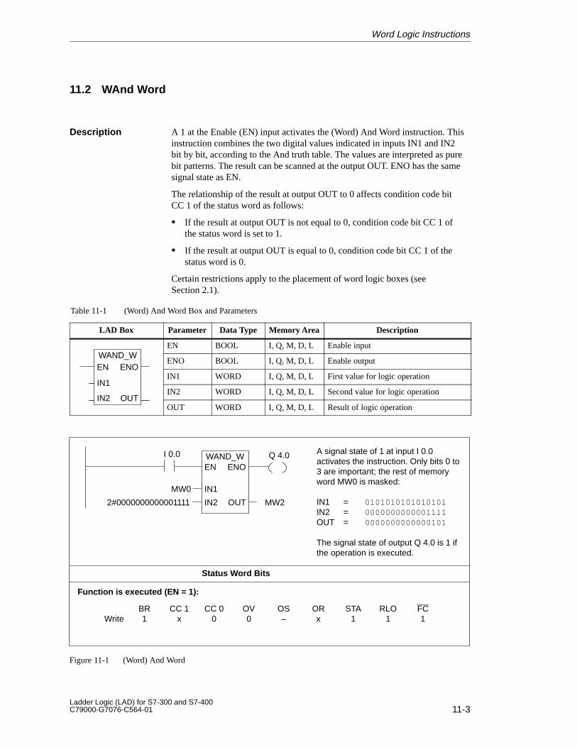
11-3Ladder Logic (LAD) for S7-300 and S7-400C79000-G7076-C564-01
11.2 WAnd Word
A 1 at the Enable (EN) input activates the (Word) And Word instruction. Thisinstruction combines the two digital values indicated in inputs IN1 and IN2bit by bit, according to the And truth table. The values are interpreted as purebit patterns. The result can be scanned at the output OUT. ENO has the samesignal state as EN.
The relationship of the result at output OUT to 0 affects condition code bitCC 1 of the status word as follows:
� If the result at output OUT is not equal to 0, condition code bit CC 1 ofthe status word is set to 1.
� If the result at output OUT is equal to 0, condition code bit CC 1 of thestatus word is 0.
Certain restrictions apply to the placement of word logic boxes (seeSection 2.1).
Table 11-1 (Word) And Word Box and Parameters
LAD Box Parameter Data Type Memory Area Description
WAND WEN BOOL I, Q, M, D, L Enable input
WAND_WEN ENO
ENO BOOL I, Q, M, D, L Enable output
IN1
EN ENOIN1 WORD I, Q, M, D, L First value for logic operation
IN1
IN2 OUTIN2 WORD I, Q, M, D, L Second value for logic operation
IN2 OUTOUT WORD I, Q, M, D, L Result of logic operation
Status Word Bits
BR CC 1 CC 0 OV OS OR STA RLO FCWrite 1 x 0 0 – x 1 1 1
I 0.0 A signal state of 1 at input I 0.0activates the instruction. Only bits 0 to3 are important; the rest of memoryword MW0 is masked:
IN1 = 0101010101010101IN2 = 0000000000001111OUT = 0000000000000101
The signal state of output Q 4.0 is 1 ifthe operation is executed.
Q 4.0WAND_W
IN2 OUT
EN ENO
2#0000000000001111 MW2
IN1MW0
Function is executed (EN = 1):
Figure 11-1 (Word) And Word
Description
Word Logic Instructions
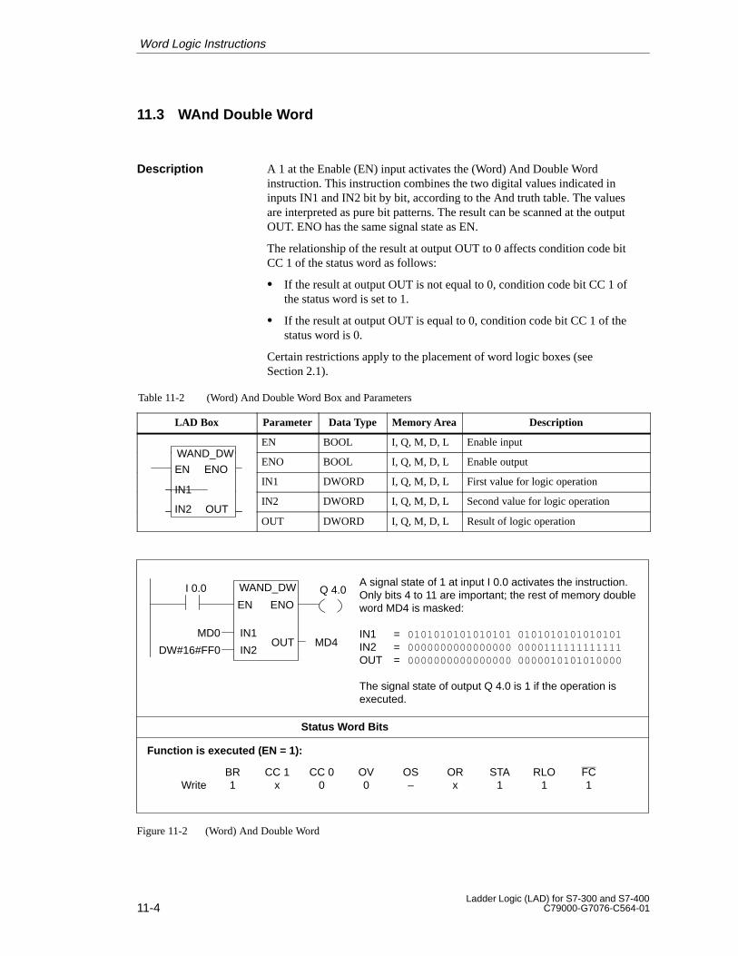
11-4Ladder Logic (LAD) for S7-300 and S7-400
C79000-G7076-C564-01
11.3 WAnd Double Word
A 1 at the Enable (EN) input activates the (Word) And Double Wordinstruction. This instruction combines the two digital values indicated ininputs IN1 and IN2 bit by bit, according to the And truth table. The valuesare interpreted as pure bit patterns. The result can be scanned at the outputOUT. ENO has the same signal state as EN.
The relationship of the result at output OUT to 0 affects condition code bitCC 1 of the status word as follows:
� If the result at output OUT is not equal to 0, condition code bit CC 1 ofthe status word is set to 1.
� If the result at output OUT is equal to 0, condition code bit CC 1 of thestatus word is 0.
Certain restrictions apply to the placement of word logic boxes (seeSection 2.1).
Table 11-2 (Word) And Double Word Box and Parameters
LAD Box Parameter Data Type Memory Area Description
WAND DWEN BOOL I, Q, M, D, L Enable input
WAND_DW
EN ENOENO BOOL I, Q, M, D, L Enable output
IN1
EN ENOIN1 DWORD I, Q, M, D, L First value for logic operation
IN1
IN2 OUTIN2 DWORD I, Q, M, D, L Second value for logic operation
IN2 OUTOUT DWORD I, Q, M, D, L Result of logic operation
Status Word Bits
BR CC 1 CC 0 OV OS OR STA RLO FCWrite 1 x 0 0 – x 1 1 1
I 0.0 A signal state of 1 at input I 0.0 activates the instruction.Only bits 4 to 11 are important; the rest of memory doubleword MD4 is masked:
IN1 = 0101010101010101 0101010101010101IN2 = 0000000000000000 0000111111111111OUT = 0000000000000000 0000010101010000
The signal state of output Q 4.0 is 1 if the operation isexecuted.
Q 4.0WAND_DW
IN2OUT
EN ENO
DW#16#FF0MD4
IN1MD0
Function is executed (EN = 1):
Figure 11-2 (Word) And Double Word
Description
Word Logic Instructions

11-5Ladder Logic (LAD) for S7-300 and S7-400C79000-G7076-C564-01
11.4 WOr Word
A 1 at the Enable (EN) input activates the (Word) Or Word instruction. Thisinstruction combines the two digital values indicated in inputs IN1 and IN2bit by bit, according to the Or truth table. The values are interpreted as purebit patterns. The result can be scanned at the output OUT. ENO has the samesignal state as EN.
The relationship of the result at output OUT to 0 affects condition code bitCC 1 of the status word as follows:
� If the result at output OUT is not equal to 0, condition code bit CC 1 ofthe status word is set to 1.
� If the result at output OUT is equal to 0, condition code bit CC 1 of thestatus word is 0.
Certain restrictions apply to the placement of word logic boxes (seeSection 2.1).
Table 11-3 (Word) Or Word Box and Parameters
LAD Box Parameter Data Type Memory Area Description
WOR WEN BOOL I, Q, M, D, L Enable input
WOR_WEN ENO
ENO BOOL I, Q, M, D, L Enable output
IN1
EN ENOIN1 WORD I, Q, M, D, L First value for logic operation
IN1
IN2 OUTIN2 WORD I, Q, M, D, L Second value for logic operation
IN2 OUTOUT WORD I, Q, M, D, L Result of logic operation
Status Word Bits
BR CC 1 CC 0 OV OS OR STA RLO FCWrite 1 x 0 0 – x 1 1 1
I 0.0A signal state of 1 at input I 0.0activates the instruction. Bits 0 to 3 areset to 1; the rest of memory word MW0remains unchanged:
IN1 = 0101010101010101IN2 = 0000000000001111OUT = 0101010101011111
The signal state of output Q 4.0 is 1 ifthe operation is executed.
Q 4.0WOR_W
IN2 OUT
EN ENO
2#0000000000001111 MW2
IN1MW0
Function is executed (EN = 1):
Figure 11-3 (Word) Or Word
Description
Word Logic Instructions

11-6Ladder Logic (LAD) for S7-300 and S7-400
C79000-G7076-C564-01
11.5 WOr Double Word
A 1 at the Enable (EN) input activates the (Word) Or Double Wordinstruction. This instruction combines the two digital values indicated ininputs IN1 and IN2 bit by bit, according to the Or truth table. The values areinterpreted as pure bit patterns. The result can be scanned at the output OUT.ENO has the same signal state as EN.
The relationship of the result at output OUT to 0 affects condition code bitCC 1 of the status word as follows:
� If the result at output OUT is not equal to 0, condition code bit CC 1 ofthe status word is set to 1.
� If the result at output OUT is equal to 0, condition code bit CC 1 of thestatus word is 0.
Certain restrictions apply to the placement of word logic boxes (seeSection 2.1).
Table 11-4 (Word) Or Double Word Box and Parameters
LAD Box Parameter Data Type Memory Area Description
WOR DWEN BOOL I, Q, M, D, L Enable input
WOR_DW
EN ENOENO BOOL I, Q, M, D, L Enable output
IN1
EN ENOIN1 DWORD I, Q, M, D, L First value for logic operation
IN1
IN2 OUTIN2 DWORD I, Q, M, D, L Second value for logic operation
IN2 OUTOUT DWORD I, Q, M, D, L Result of logic operation
Status Word Bits
BR CC 1 CC 0 OV OS OR STA RLO FCRead * – – – – * – * *Write 1 x 0 0 – x 1 1 1
I 0.0 A signal state of 1 at input I 0.0 activates the instruction.Bits 0 to 11 are set to 1; the rest of memory double wordMD4 remains unchanged:
IN1 = 0101010101010101 0101010101010101IN2 = 0000000000000000 0000111111111111OUT = 0101010101010101 0101111111111111
The signal state of output Q 4.0 is 1 if the operation isexecuted.
Q 4.0WOR_DW
IN2OUT
EN ENO
DW#16#FFFMD4
IN1MD0
Function is executed (EN = 1):
Figure 11-4 (Word) Or Double Word
Description
Word Logic Instructions
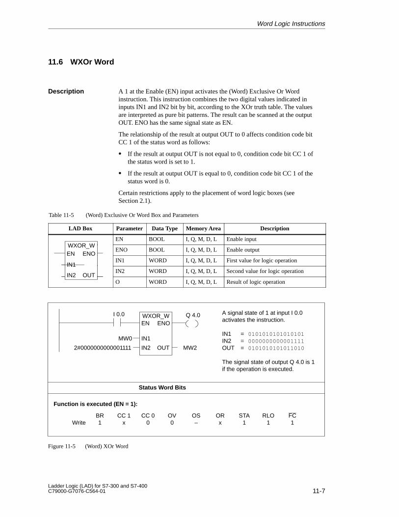
11-7Ladder Logic (LAD) for S7-300 and S7-400C79000-G7076-C564-01
11.6 WXOr Word
A 1 at the Enable (EN) input activates the (Word) Exclusive Or Wordinstruction. This instruction combines the two digital values indicated ininputs IN1 and IN2 bit by bit, according to the XOr truth table. The valuesare interpreted as pure bit patterns. The result can be scanned at the outputOUT. ENO has the same signal state as EN.
The relationship of the result at output OUT to 0 affects condition code bitCC 1 of the status word as follows:
� If the result at output OUT is not equal to 0, condition code bit CC 1 ofthe status word is set to 1.
� If the result at output OUT is equal to 0, condition code bit CC 1 of thestatus word is 0.
Certain restrictions apply to the placement of word logic boxes (seeSection 2.1).
Table 11-5 (Word) Exclusive Or Word Box and Parameters
LAD Box Parameter Data Type Memory Area Description
WXOR WEN BOOL I, Q, M, D, L Enable input
WXOR_WEN ENO
ENO BOOL I, Q, M, D, L Enable output
IN1
EN ENOIN1 WORD I, Q, M, D, L First value for logic operation
IN1
IN2 OUTIN2 WORD I, Q, M, D, L Second value for logic operation
IN2 OUTO WORD I, Q, M, D, L Result of logic operation
Status Word Bits
BR CC 1 CC 0 OV OS OR STA RLO FCWrite 1 x 0 0 – x 1 1 1
I 0.0 Q 4.0WXOR_W
IN2 OUT
EN ENO
2#0000000000001111 MW2
IN1MW0
Function is executed (EN = 1):
A signal state of 1 at input I 0.0activates the instruction.
IN1 = 0101010101010101IN2 = 0000000000001111OUT = 0101010101011010
The signal state of output Q 4.0 is 1if the operation is executed.
Figure 11-5 (Word) XOr Word
Description
Word Logic Instructions
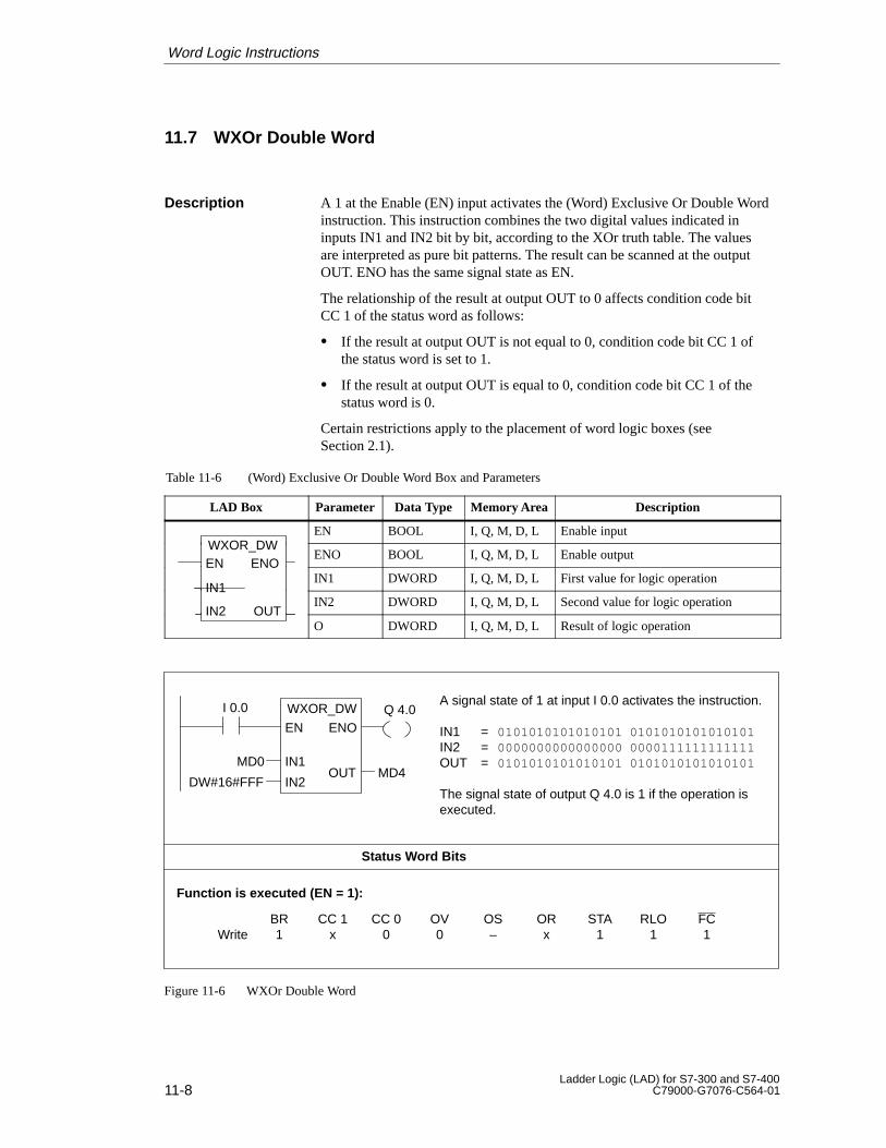
11-8Ladder Logic (LAD) for S7-300 and S7-400
C79000-G7076-C564-01
11.7 WXOr Double Word
A 1 at the Enable (EN) input activates the (Word) Exclusive Or Double Wordinstruction. This instruction combines the two digital values indicated ininputs IN1 and IN2 bit by bit, according to the XOr truth table. The valuesare interpreted as pure bit patterns. The result can be scanned at the outputOUT. ENO has the same signal state as EN.
The relationship of the result at output OUT to 0 affects condition code bitCC 1 of the status word as follows:
� If the result at output OUT is not equal to 0, condition code bit CC 1 ofthe status word is set to 1.
� If the result at output OUT is equal to 0, condition code bit CC 1 of thestatus word is 0.
Certain restrictions apply to the placement of word logic boxes (seeSection 2.1).
Table 11-6 (Word) Exclusive Or Double Word Box and Parameters
LAD Box Parameter Data Type Memory Area Description
WXOR DWEN BOOL I, Q, M, D, L Enable input
WXOR_DWEN ENO
ENO BOOL I, Q, M, D, L Enable output
IN1
EN ENOIN1 DWORD I, Q, M, D, L First value for logic operation
IN1
IN2 OUTIN2 DWORD I, Q, M, D, L Second value for logic operation
IN2 OUTO DWORD I, Q, M, D, L Result of logic operation
Status Word Bits
BR CC 1 CC 0 OV OS OR STA RLO FCWrite 1 x 0 0 – x 1 1 1
I 0.0 A signal state of 1 at input I 0.0 activates the instruction.
IN1 = 0101010101010101 0101010101010101IN2 = 0000000000000000 0000111111111111OUT = 0101010101010101 0101010101010101
The signal state of output Q 4.0 is 1 if the operation isexecuted.
Q 4.0WXOR_DW
IN2OUT
EN ENO
DW#16#FFFMD4
IN1MD0
Function is executed (EN = 1):
Figure 11-6 WXOr Double Word
Description
Word Logic Instructions
12-1Ladder Logic (LAD) for S7-300 and S7-400C79000-G7076-C564-01
Shift and Rotate Instructions
Section Description Page
12.1 Shift Instructions 12-2
12.2 Rotate Instructions 12-10
Chapter Overview
12
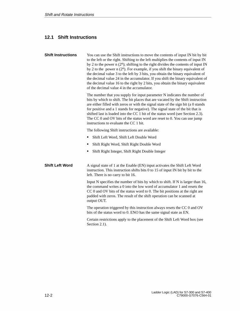
12-2Ladder Logic (LAD) for S7-300 and S7-400
C79000-G7076-C564-01
12.1 Shift Instructions
You can use the Shift instructions to move the contents of input IN bit by bitto the left or the right. Shifting to the left multiplies the contents of input INby 2 to the power n (2n); shifting to the right divides the contents of input INby 2 to the power n (2n). For example, if you shift the binary equivalent ofthe decimal value 3 to the left by 3 bits, you obtain the binary equivalent ofthe decimal value 24 in the accumulator. If you shift the binary equivalent ofthe decimal value 16 to the right by 2 bits, you obtain the binary equivalentof the decimal value 4 in the accumulator.
The number that you supply for input parameter N indicates the number ofbits by which to shift. The bit places that are vacated by the Shift instructionare either filled with zeros or with the signal state of the sign bit (a 0 standsfor positive and a 1 stands for negative). The signal state of the bit that isshifted last is loaded into the CC 1 bit of the status word (see Section 2.3).The CC 0 and OV bits of the status word are reset to 0. You can use jumpinstructions to evaluate the CC 1 bit.
The following Shift instructions are available:
� Shift Left Word, Shift Left Double Word
� Shift Right Word, Shift Right Double Word
� Shift Right Integer, Shift Right Double Integer
A signal state of 1 at the Enable (EN) input activates the Shift Left Wordinstruction. This instruction shifts bits 0 to 15 of input IN bit by bit to theleft. There is no carry to bit 16.
Input N specifies the number of bits by which to shift. If N is larger than 16,the command writes a 0 into the low word of accumulator 1 and resets theCC 0 and OV bits of the status word to 0. The bit positions at the right arepadded with zeros. The result of the shift operation can be scanned atoutput OUT.
The operation triggered by this instruction always resets the CC 0 and OVbits of the status word to 0. ENO has the same signal state as EN.
Certain restrictions apply to the placement of the Shift Left Word box (seeSection 2.1).
Shift Instructions
Shift Left Word
Shift and Rotate Instructions
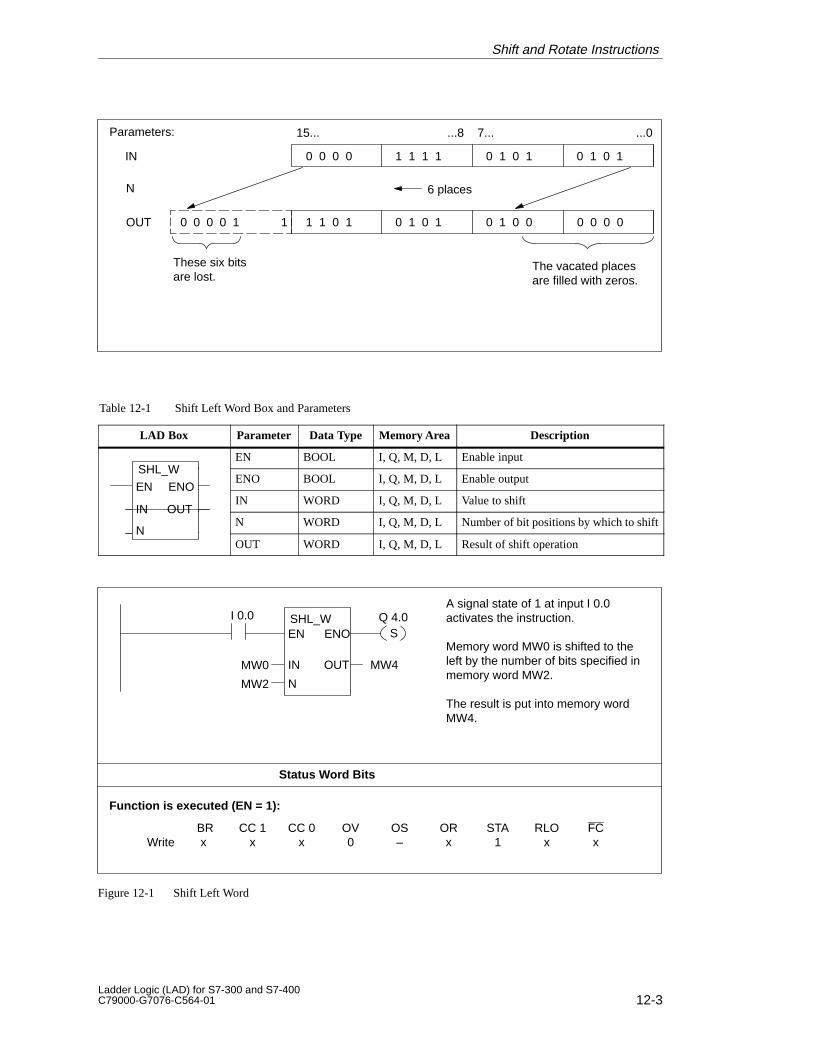
12-3Ladder Logic (LAD) for S7-300 and S7-400C79000-G7076-C564-01
15... ...8 7... ...0
0 1 0 1
0 1 0 1 0 1 0 10 0 0 0
0 1 0 01 1 0 1
IN
N
OUT 0 0 0 0
1 1 1 1
0 0 0 0 1 1
6 places
Parameters:
These six bitsare lost.
The vacated placesare filled with zeros.
Table 12-1 Shift Left Word Box and Parameters
LAD Box Parameter Data Type Memory Area Description
SHL WEN BOOL I, Q, M, D, L Enable input
SHL_W
EN ENOENO BOOL I, Q, M, D, L Enable output
IN
EN
OUT
ENOIN WORD I, Q, M, D, L Value to shift
IN
N
OUTN WORD I, Q, M, D, L Number of bit positions by which to shift
NOUT WORD I, Q, M, D, L Result of shift operation
Status Word Bits
BR CC 1 CC 0 OV OS OR STA RLO FCWrite x x x 0 – x 1 x x
I 0.0A signal state of 1 at input I 0.0activates the instruction.
Memory word MW0 is shifted to theleft by the number of bits specified inmemory word MW2.
The result is put into memory wordMW4.
Q 4.0SHL_W
N
OUT
EN ENO
MW2
IN
Function is executed (EN = 1):
MW4MW0
S
Figure 12-1 Shift Left Word
Shift and Rotate Instructions
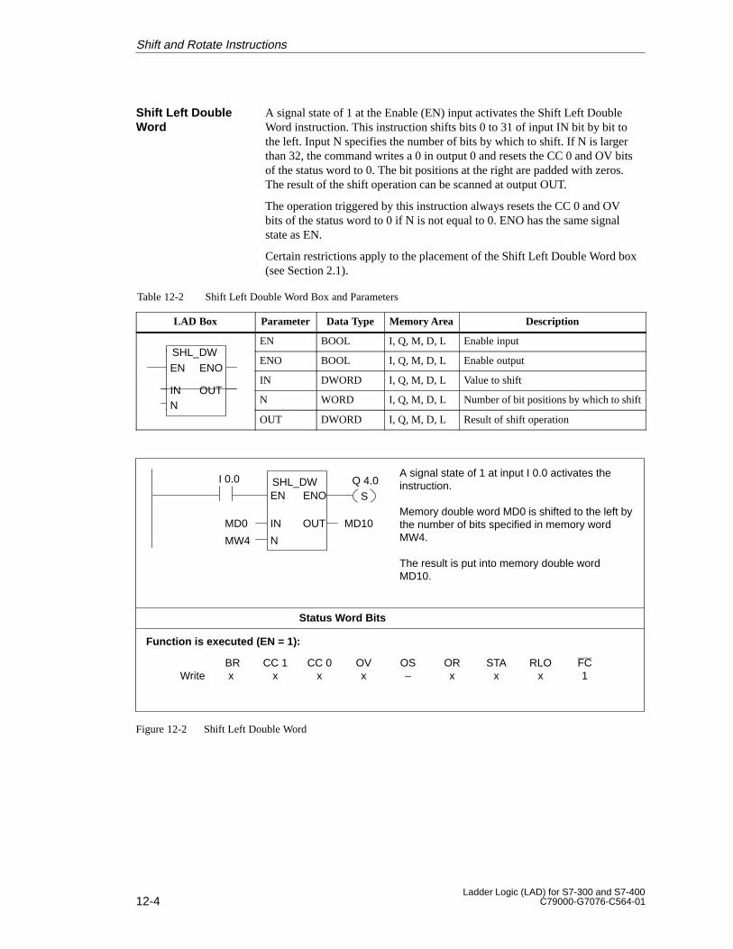
12-4Ladder Logic (LAD) for S7-300 and S7-400
C79000-G7076-C564-01
A signal state of 1 at the Enable (EN) input activates the Shift Left DoubleWord instruction. This instruction shifts bits 0 to 31 of input IN bit by bit tothe left. Input N specifies the number of bits by which to shift. If N is largerthan 32, the command writes a 0 in output 0 and resets the CC 0 and OV bitsof the status word to 0. The bit positions at the right are padded with zeros.The result of the shift operation can be scanned at output OUT.
The operation triggered by this instruction always resets the CC 0 and OVbits of the status word to 0 if N is not equal to 0. ENO has the same signalstate as EN.
Certain restrictions apply to the placement of the Shift Left Double Word box(see Section 2.1).
Table 12-2 Shift Left Double Word Box and Parameters
LAD Box Parameter Data Type Memory Area Description
SHL DWEN BOOL I, Q, M, D, L Enable input
SHL_DW
EN ENOENO BOOL I, Q, M, D, L Enable output
IN
EN
OUT
ENOIN DWORD I, Q, M, D, L Value to shift
INN
OUTN WORD I, Q, M, D, L Number of bit positions by which to shiftNOUT DWORD I, Q, M, D, L Result of shift operation
Status Word Bits
BR CC 1 CC 0 OV OS OR STA RLO FCWrite x x x x – x x x 1
I 0.0 A signal state of 1 at input I 0.0 activates theinstruction.
Memory double word MD0 is shifted to the left bythe number of bits specified in memory wordMW4.
The result is put into memory double wordMD10.
Q 4.0SHL_DW
N
OUT
EN ENO
MW4
IN
Function is executed (EN = 1):
MD10MD0
S
Figure 12-2 Shift Left Double Word
Shift Left DoubleWord
Shift and Rotate Instructions
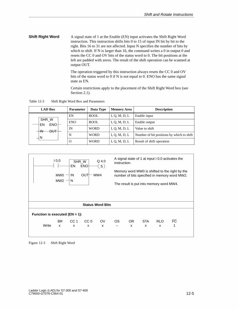
12-5Ladder Logic (LAD) for S7-300 and S7-400C79000-G7076-C564-01
A signal state of 1 at the Enable (EN) input activates the Shift Right Wordinstruction. This instruction shifts bits 0 to 15 of input IN bit by bit to theright. Bits 16 to 31 are not affected. Input N specifies the number of bits bywhich to shift. If N is larger than 16, the command writes a 0 in output 0 andresets the CC 0 and OV bits of the status word to 0. The bit positions at theleft are padded with zeros. The result of the shift operation can be scanned atoutput OUT.
The operation triggered by this instruction always resets the CC 0 and OVbits of the status word to 0 if N is not equal to 0. ENO has the same signalstate as EN.
Certain restrictions apply to the placement of the Shift Right Word box (seeSection 2.1).
Table 12-3 Shift Right Word Box and Parameters
LAD Box Parameter Data Type Memory Area Description
SHR WEN BOOL I, Q, M, D, L Enable input
SHR_W
EN ENOENO BOOL I, Q, M, D, L Enable output
IN
EN
OUT
ENOIN WORD I, Q, M, D, L Value to shift
IN
N
OUTN WORD I, Q, M, D, L Number of bit positions by which to shift
NO WORD I, Q, M, D, L Result of shift operation
Status Word Bits
BR CC 1 CC 0 OV OS OR STA RLO FCWrite x x x x – x x x 1
I 0.0 A signal state of 1 at input I 0.0 activates theinstruction.
Memory word MW0 is shifted to the right by thenumber of bits specified in memory word MW2.
The result is put into memory word MW4.
Q 4.0SHR_W
N
OUT
EN ENO
MW2
IN
Function is executed (EN = 1):
MW4MW0
S
Figure 12-3 Shift Right Word
Shift Right Word
Shift and Rotate Instructions
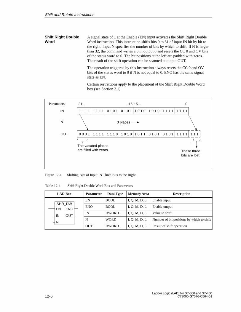
12-6Ladder Logic (LAD) for S7-300 and S7-400
C79000-G7076-C564-01
A signal state of 1 at the Enable (EN) input activates the Shift Right DoubleWord instruction. This instruction shifts bits 0 to 31 of input IN bit by bit tothe right. Input N specifies the number of bits by which to shift. If N is largerthan 32, the command writes a 0 in output 0 and resets the CC 0 and OV bitsof the status word to 0. The bit positions at the left are padded with zeros.The result of the shift operation can be scanned at output OUT.
The operation triggered by this instruction always resets the CC 0 and OVbits of the status word to 0 if N is not equal to 0. ENO has the same signalstate as EN.
Certain restrictions apply to the placement of the Shift Right Double Wordbox (see Section 2.1).
1 1 1
31... ...16 15... ...0
1 1 1 1 1 1 1 1 0 1 0 1 0 1 0 1 1 0 1 0 1 0 1 0 1 1 1 1 1 1 1 1
0 1 0 10 0 0 1 1 1 1 1 1 1 1 0 1 0 1 0 1 0 1 1 0 1 0 1 1 1 1 1
3 places
The vacated placesare filled with zeros. These three
bits are lost.
IN
N
OUT
Parameters:
Figure 12-4 Shifting Bits of Input IN Three Bits to the Right
Table 12-4 Shift Right Double Word Box and Parameters
LAD Box Parameter Data Type Memory Area Description
SHR DWEN BOOL I, Q, M, D, L Enable input
SHR_DW
EN ENOENO BOOL I, Q, M, D, L Enable output
IN
EN
OUT
ENOIN DWORD I, Q, M, D, L Value to shift
IN
N
OUTN WORD I, Q, M, D, L Number of bit positions by which to shift
NOUT DWORD I, Q, M, D, L Result of shift operation
Shift Right DoubleWord
Shift and Rotate Instructions
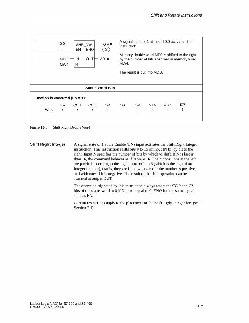
12-7Ladder Logic (LAD) for S7-300 and S7-400C79000-G7076-C564-01
Status Word Bits
BR CC 1 CC 0 OV OS OR STA RLO FCWrite x x x x – x x x 1
I 0.0 A signal state of 1 at input I 0.0 activates theinstruction.
Memory double word MD0 is shifted to the rightby the number of bits specified in memory wordMW4.
The result is put into MD10.
Q 4.0SHR_DW
N
OUT
MW4
IN
Function is executed (EN = 1):
MD10MD0
SEN ENO
Figure 12-5 Shift Right Double Word
A signal state of 1 at the Enable (EN) input activates the Shift Right Integerinstruction. This instruction shifts bits 0 to 15 of input IN bit by bit to theright. Input N specifies the number of bits by which to shift. If N is largerthan 16, the command behaves as if N were 16. The bit positions at the leftare padded according to the signal state of bit 15 (which is the sign of aninteger number), that is, they are filled with zeros if the number is positive,and with ones if it is negative. The result of the shift operation can bescanned at output OUT.
The operation triggered by this instruction always resets the CC 0 and OVbits of the status word to 0 if N is not equal to 0. ENO has the same signalstate as EN.
Certain restrictions apply to the placement of the Shift Right Integer box (seeSection 2.1).
Shift Right Integer
Shift and Rotate Instructions
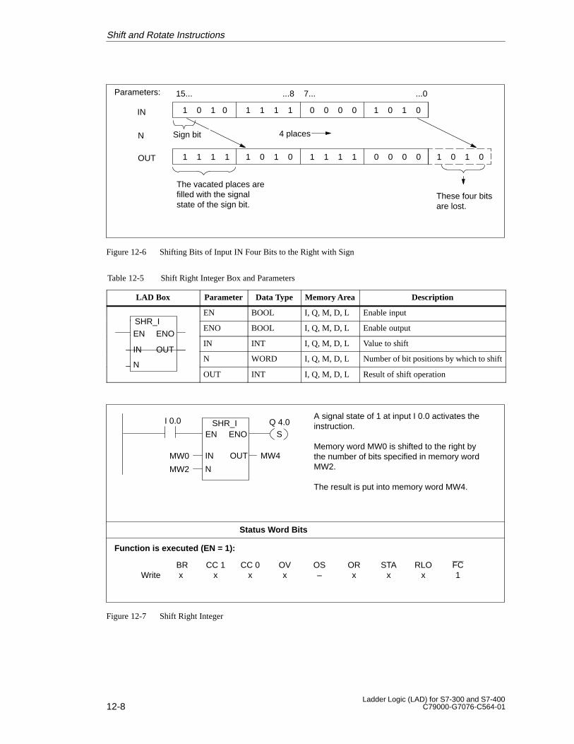
12-8Ladder Logic (LAD) for S7-300 and S7-400
C79000-G7076-C564-01
15... ...8 7... ...0
1 0 1 0
0 0 0 0 1 0 1 01 0 1 0
1 1 1 11 1 1 1 0 0 0 0
1 1 1 1
4 places
The vacated places arefilled with the signalstate of the sign bit.
1 0 1 0
These four bitsare lost.
Sign bit
IN
N
OUT
Parameters:
Figure 12-6 Shifting Bits of Input IN Four Bits to the Right with Sign
Table 12-5 Shift Right Integer Box and Parameters
LAD Box Parameter Data Type Memory Area Description
SHR IEN BOOL I, Q, M, D, L Enable input
SHR_I
EN ENOENO BOOL I, Q, M, D, L Enable output
IN
EN
OUT
ENOIN INT I, Q, M, D, L Value to shift
IN
N
OUTN WORD I, Q, M, D, L Number of bit positions by which to shift
NOUT INT I, Q, M, D, L Result of shift operation
Status Word Bits
BR CC 1 CC 0 OV OS OR STA RLO FCWrite x x x x – x x x 1
I 0.0 A signal state of 1 at input I 0.0 activates theinstruction.
Memory word MW0 is shifted to the right bythe number of bits specified in memory wordMW2.
The result is put into memory word MW4.
Q 4.0SHR_I
N
OUT
MW2
IN
Function is executed (EN = 1):
MW4MW0
SEN ENO
Figure 12-7 Shift Right Integer
Shift and Rotate Instructions
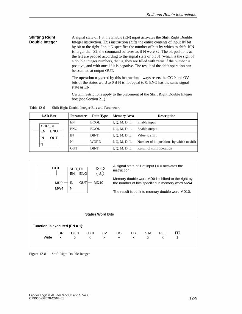
12-9Ladder Logic (LAD) for S7-300 and S7-400C79000-G7076-C564-01
A signal state of 1 at the Enable (EN) input activates the Shift Right DoubleInteger instruction. This instruction shifts the entire contents of input IN bitby bit to the right. Input N specifies the number of bits by which to shift. If Nis larger than 32, the command behaves as if N were 32. The bit positions atthe left are padded according to the signal state of bit 31 (which is the sign ofa double integer number), that is, they are filled with zeros if the number ispositive, and with ones if it is negative. The result of the shift operation canbe scanned at output OUT.
The operation triggered by this instruction always resets the CC 0 and OVbits of the status word to 0 if N is not equal to 0. ENO has the same signalstate as EN.
Certain restrictions apply to the placement of the Shift Right Double Integerbox (see Section 2.1).
Table 12-6 Shift Right Double Integer Box and Parameters
LAD Box Parameter Data Type Memory Area Description
SHR DIEN BOOL I, Q, M, D, L Enable input
SHR_DI
EN ENOENO BOOL I, Q, M, D, L Enable output
IN
EN
OUT
ENOIN DINT I, Q, M, D, L Value to shift
IN
N
OUTN WORD I, Q, M, D, L Number of bit positions by which to shift
NOUT DINT I, Q, M, D, L Result of shift operation
Status Word Bits
BR CC 1 CC 0 OV OS OR STA RLO FCWrite x x x x – x x x 1
I 0.0 A signal state of 1 at input I 0.0 activates theinstruction.
Memory double word MD0 is shifted to the right bythe number of bits specified in memory word MW4.
The result is put into memory double word MD10.
Q 4.0SHR_DI
N
OUT
MW4
IN
Function is executed (EN = 1):
MD10MD0
SEN ENO
Figure 12-8 Shift Right Double Integer
Shifting RightDouble Integer
Shift and Rotate Instructions
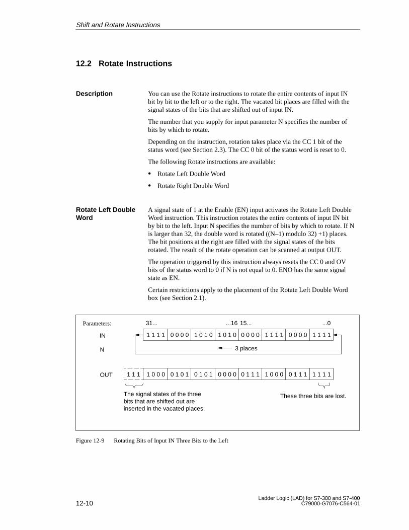
12-10Ladder Logic (LAD) for S7-300 and S7-400
C79000-G7076-C564-01
12.2 Rotate Instructions
You can use the Rotate instructions to rotate the entire contents of input INbit by bit to the left or to the right. The vacated bit places are filled with thesignal states of the bits that are shifted out of input IN.
The number that you supply for input parameter N specifies the number ofbits by which to rotate.
Depending on the instruction, rotation takes place via the CC 1 bit of thestatus word (see Section 2.3). The CC 0 bit of the status word is reset to 0.
The following Rotate instructions are available:
� Rotate Left Double Word
� Rotate Right Double Word
A signal state of 1 at the Enable (EN) input activates the Rotate Left DoubleWord instruction. This instruction rotates the entire contents of input IN bitby bit to the left. Input N specifies the number of bits by which to rotate. If Nis larger than 32, the double word is rotated ((N–1) modulo 32) +1) places.The bit positions at the right are filled with the signal states of the bitsrotated. The result of the rotate operation can be scanned at output OUT.
The operation triggered by this instruction always resets the CC 0 and OVbits of the status word to 0 if N is not equal to 0. ENO has the same signalstate as EN.
Certain restrictions apply to the placement of the Rotate Left Double Wordbox (see Section 2.1).
1 1 1
31... ...16 15... ...0
1 1 1 1 0 0 0 0 1 0 1 0 1 0 1 0 0 0 0 0 1 1 1 1 0 0 0 0 1 1 1 1
0 1 1 11 0 0 0 0 1 0 1 0 1 0 1 0 0 0 0 0 1 1 1 1 0 0 0 1 1 1 1
3 places
The signal states of the threebits that are shifted out areinserted in the vacated places.
These three bits are lost.
IN
N
OUT
Parameters:
Figure 12-9 Rotating Bits of Input IN Three Bits to the Left
Description
Rotate Left DoubleWord
Shift and Rotate Instructions

12-11Ladder Logic (LAD) for S7-300 and S7-400C79000-G7076-C564-01
Table 12-7 Rotate Left Double Word Box and Parameters
LAD Box Parameter Data Type Memory Area Description
EN BOOL I, Q, M, D, L Enable input
ROL_DW
EN ENOENO BOOL I, Q, M, D, L Enable output
IN
EN
OUT
ENO IN DWORD I, Q, M, D, L Value to rotateIN
N
OUTN WORD I, Q, M, D, L
Number of bit positions by which torotate
OUT DWORD I, Q, M, D, L Result of rotate operation
Status Word Bits
BR CC 1 CC 0 OV OS OR STA RLO FCWrite x x x x – x x x 1
I 0.0 A signal state of 1 at input I 0.0 activates theinstruction.
Memory double word MD0 is rotated to the leftby the number of bits specified in memory wordMW4.
The result is put into memory double wordMD10.
Q 4.0ROL_DW
N
OUT
EN ENO
MW4
IN
Function is executed (EN = 1):
MD10MD0
S
Figure 12-10 Rotate Left Double Word
A signal state of 1 at the Enable (EN) input activates the Rotate Right DoubleWord instruction. This instruction rotates the entire contents of input IN bitby bit to the right. Input N specifies the number of bits by which to rotate.The value of N can be between 0 and 31. If N is larger than 32, the doubleword is rotated ((N–1) modulo 32) +1) places. The bit positions at the left arefilled with the signal states of the bits rotated. The result of the rotateoperation can be scanned at output OUT.
The operation triggered by this instruction always resets the CC 0 and OVbits of the status word to 0 if N is not equal to 0. ENO has the same signalstate as EN.
Certain restrictions apply to the placement of the Rotate Right Double Wordbox (see Section 2.1).
Rotate RightDouble Word
Shift and Rotate Instructions
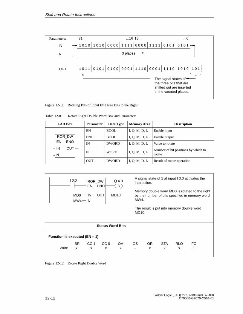
12-12Ladder Logic (LAD) for S7-300 and S7-400
C79000-G7076-C564-01
1 0 1
31... ...16 15... ...0
1 0 1 0 1 0 1 0 0 0 0 0 1 1 1 1 0 0 0 0 1 1 1 1 0 1 0 1 0 1 0 1
1 1 1 01 0 1 1 0 1 0 1 0 1 0 0 0 0 0 1 1 1 1 0 0 0 0 1 1 0 1 0
3 places
The signal states ofthe three bits that areshifted out are insertedin the vacated places.
IN
N
OUT
Parameters:
Figure 12-11 Rotating Bits of Input IN Three Bits to the Right
Table 12-8 Rotate Right Double Word Box and Parameters
LAD Box Parameter Data Type Memory Area Description
EN BOOL I, Q, M, D, L Enable input
ROR_DW
EN ENOENO BOOL I, Q, M, D, L Enable output
IN
EN
OUT
ENO IN DWORD I, Q, M, D, L Value to rotateIN
N
OUTN WORD I, Q, M, D, L
Number of bit positions by which torotate
OUT DWORD I, Q, M, D, L Result of rotate operation
Status Word Bits
BR CC 1 CC 0 OV OS OR STA RLO FCWrite x x x x – x x x 1
I 0.0 A signal state of 1 at input I 0.0 activates theinstruction.
Memory double word MD0 is rotated to the rightby the number of bits specified in memory wordMW4.
The result is put into memory double wordMD10.
Q 4.0ROR_DW
N
OUT
MW4
IN
Function is executed (EN = 1):
MD10MD0
SENOEN
Figure 12-12 Rotate Right Double Word
Shift and Rotate Instructions
13-1Ladder Logic (LAD) for S7-300 and S7-400C79000-G7076-C564-01
Data Block Instructions
Section Description Page
13.1 Open Data Block: DB or DI 13-2
Chapter Overview
13
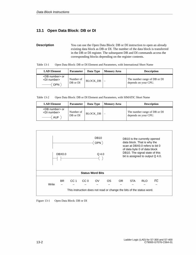
13-2Ladder Logic (LAD) for S7-300 and S7-400
C79000-G7076-C564-01
13.1 Open Data Block: DB or DI
You can use the Open Data Block: DB or DI instruction to open an alreadyexisting data block as DB or DI. The number of the data block is transferredin the DB or DI register. The subsequent DB and DI commands access thecorresponding blocks depending on the register contents.
Table 13-1 Open Data Block: DB or DI Element and Parameters, with International Short Name
LAD Element Parameter Data Type Memory Area Description
<DB number> or<DI number>
OPN
Number ofDB or DI
BLOCK_DB –The number range of DB or DI depends on your CPU.
Table 13-2 Open Data Block: DB or DI Element and Parameters, with SIMATIC Short Name
LAD Element Parameter Data Type Memory Area Description
<DB number> or<DI number>
AUF
Number ofDB or DI
BLOCK_DB –The number range of DB or DI depends on your CPU.
Status Word Bits
BR CC 1 CC 0 OV OS OR STA RLO FCWrite – – – – – – – – –
DB10 is the currently openeddata block. That is why thescan at DBX0.0 refers to bit 0of data byte 0 of data blockDB10. The signal state of thisbit is assigned to output Q 4.0.
OPN
DB10
DBX0.0 Q 4.0
This instruction does not read or change the bits of the status word.
Figure 13-1 Open Data Block: DB or DI
Description
Data Block Instructions
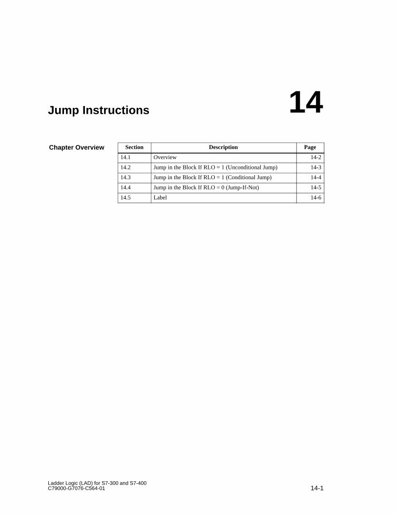
14-1Ladder Logic (LAD) for S7-300 and S7-400C79000-G7076-C564-01
Jump Instructions
Section Description Page
14.1 Overview 14-2
14.2 Jump in the Block If RLO = 1 (Unconditional Jump) 14-3
14.3 Jump in the Block If RLO = 1 (Conditional Jump) 14-4
14.4 Jump in the Block If RLO = 0 (Jump-If-Not) 14-5
14.5 Label 14-6
Chapter Overview
14
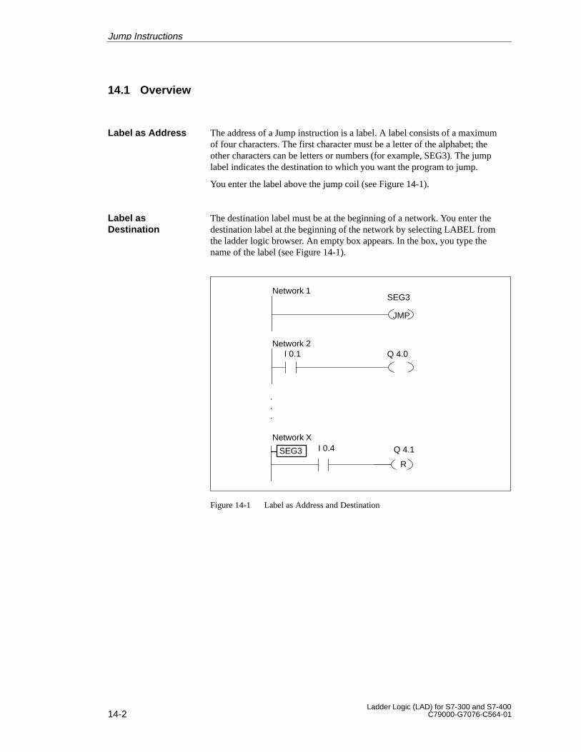
14-2Ladder Logic (LAD) for S7-300 and S7-400
C79000-G7076-C564-01
14.1 Overview
The address of a Jump instruction is a label. A label consists of a maximumof four characters. The first character must be a letter of the alphabet; theother characters can be letters or numbers (for example, SEG3). The jumplabel indicates the destination to which you want the program to jump.
You enter the label above the jump coil (see Figure 14-1).
The destination label must be at the beginning of a network. You enter thedestination label at the beginning of the network by selecting LABEL fromthe ladder logic browser. An empty box appears. In the box, you type thename of the label (see Figure 14-1).
SEG3
SEG3
JMP
R
I 0.4 Q 4.1
Network 1
Network X
Q 4.0Network 2
.
.
.
I 0.1
Figure 14-1 Label as Address and Destination
Label as Address
Label asDestination
Jump Instructions
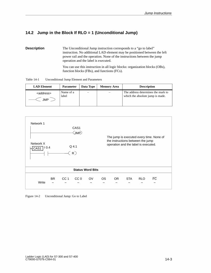
14-3Ladder Logic (LAD) for S7-300 and S7-400C79000-G7076-C564-01
14.2 Jump in the Block If RLO = 1 (Unconditional Jump)
The Unconditional Jump instruction corresponds to a “go to label”instruction. No additional LAD element may be positioned between the leftpower rail and the operation. None of the instructions between the jumpoperation and the label is executed.
You can use this instruction in all logic blocks: organization blocks (OBs),function blocks (FBs), and functions (FCs).
Table 14-1 Unconditional Jump Element and Parameters
LAD Element Parameter Data Type Memory Area Description
JMP
<address> Name of alabel
– – The address determines the mark towhich the absolute jump is made.
Status Word Bits
BR CC 1 CC 0 OV OS OR STA RLO FCWrite – – – – – – – – –
CAS1
CAS1
JMP
R
I 0.4 Q 4.1
Network 1
Network X
The jump is executed every time. None ofthe instructions between the jumpoperation and the label is executed.
Figure 14-2 Unconditional Jump: Go to Label
Description
Jump Instructions
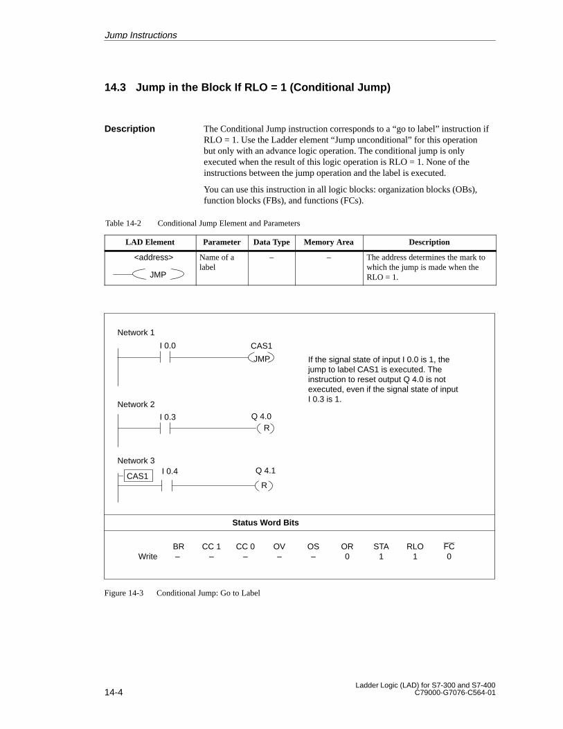
14-4Ladder Logic (LAD) for S7-300 and S7-400
C79000-G7076-C564-01
14.3 Jump in the Block If RLO = 1 (Conditional Jump)
The Conditional Jump instruction corresponds to a “go to label” instruction ifRLO = 1. Use the Ladder element “Jump unconditional” for this operationbut only with an advance logic operation. The conditional jump is onlyexecuted when the result of this logic operation is RLO = 1. None of theinstructions between the jump operation and the label is executed.
You can use this instruction in all logic blocks: organization blocks (OBs),function blocks (FBs), and functions (FCs).
Table 14-2 Conditional Jump Element and Parameters
LAD Element Parameter Data Type Memory Area Description
JMP
<address> Name of alabel
– – The address determines the mark towhich the jump is made when theRLO = 1.
JMP
Network 1
Status Word Bits
BR CC 1 CC 0 OV OS OR STA RLO FCWrite – – – – – 0 1 1 0
I 0.0
Q 4.0I 0.3
If the signal state of input I 0.0 is 1, thejump to label CAS1 is executed. Theinstruction to reset output Q 4.0 is notexecuted, even if the signal state of inputI 0.3 is 1.
CAS1
Q 4.1I 0.4Network 3
R
R
CAS1
Network 2
Figure 14-3 Conditional Jump: Go to Label
Description
Jump Instructions
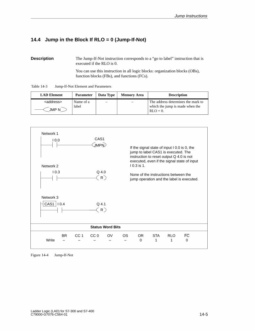
14-5Ladder Logic (LAD) for S7-300 and S7-400C79000-G7076-C564-01
14.4 Jump in the Block If RLO = 0 (Jump-If-Not)
The Jump-If-Not instruction corresponds to a “go to label” instruction that isexecuted if the RLO is 0.
You can use this instruction in all logic blocks: organization blocks (OBs),function blocks (FBs), and functions (FCs).
Table 14-3 Jump-If-Not Element and Parameters
LAD Element Parameter Data Type Memory Area Description
JMP N
<address> Name of alabel
– – The address determines the mark towhich the jump is made when theRLO = 0.
Status Word Bits
BR CC 1 CC 0 OV OS OR STA RLO FCWrite – – – – – 0 1 1 0
CAS1
JMPN
R
I 0.4 Q 4.1
Network 1
Network 3
If the signal state of input I 0.0 is 0, thejump to label CAS1 is executed. Theinstruction to reset output Q 4.0 is notexecuted, even if the signal state of inputI 0.3 is 1.
None of the instructions between thejump operation and the label is executed.
I 0.0
R
I 0.3 Q 4.0
CAS1
Network 2
Figure 14-4 Jump-If-Not
Description
Jump Instructions
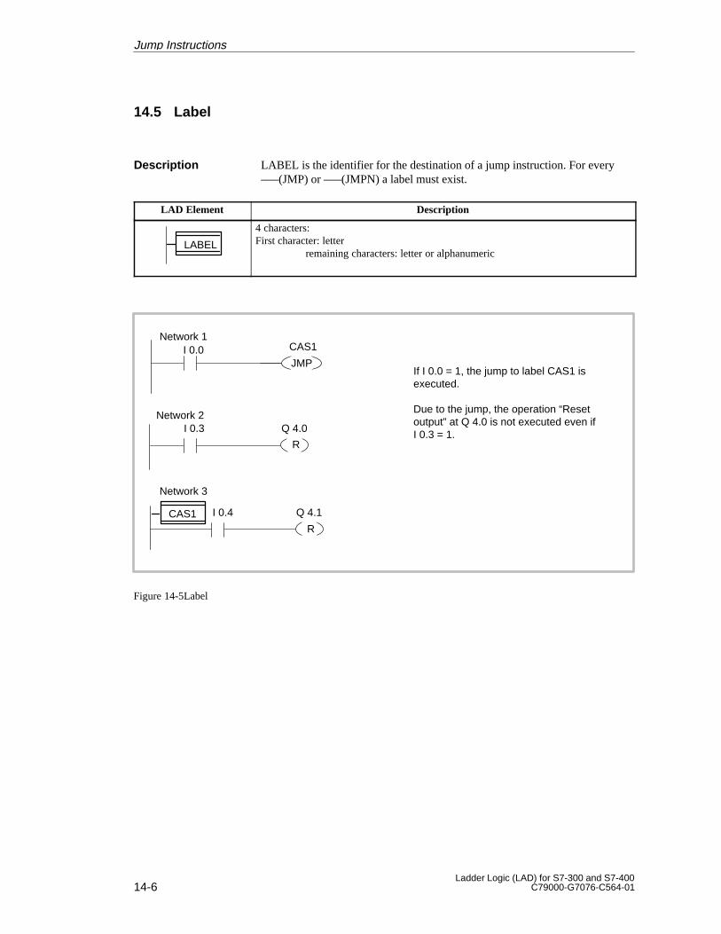
14-6Ladder Logic (LAD) for S7-300 and S7-400
C79000-G7076-C564-01
14.5 Label
LABEL is the identifier for the destination of a jump instruction. For every–––(JMP) or –––(JMPN) a label must exist.
LAD Element Description
LABEL
4 characters:First character: letter
remaining characters: letter or alphanumeric
CAS1
JMP
R
I 0.4 Q 4.1
Network 1
Network 3
If I 0.0 = 1, the jump to label CAS1 isexecuted.
Due to the jump, the operation “Resetoutput” at Q 4.0 is not executed even ifI 0.3 = 1.
I 0.0
R
I 0.3 Q 4.0Network 2
CAS1
Figure 14-5Label
Description
Jump Instructions
15-1Ladder Logic (LAD) for S7-300 and S7-400C79000-G7076-C564-01
Status Bit Instructions
Section Description Page
15.1 Overview 15-2
15.2 Exception Bit BR Memory 15-3
15.3 Result Bits 15-4
15.4 Result Bit Unordered 15-6
15.5 Exception Bit Overflow 15-7
15.6 Exception Bit Overflow Stored 15-9
Chapter Overview
15
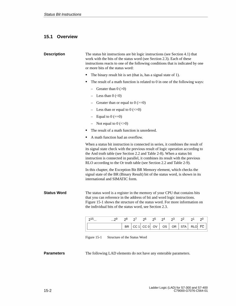
15-2Ladder Logic (LAD) for S7-300 and S7-400
C79000-G7076-C564-01
15.1 Overview
The status bit instructions are bit logic instructions (see Section 4.1) thatwork with the bits of the status word (see Section 2.3). Each of theseinstructions reacts to one of the following conditions that is indicated by oneor more bits of the status word:
� The binary result bit is set (that is, has a signal state of 1).
� The result of a math function is related to 0 in one of the following ways:
– Greater than 0 (>0)
– Less than 0 (<0)
– Greater than or equal to 0 (>=0)
– Less than or equal to 0 (<=0)
– Equal to 0 (==0)
– Not equal to 0 (<>0)
� The result of a math function is unordered.
� A math function had an overflow.
When a status bit instruction is connected in series, it combines the result ofits signal state check with the previous result of logic operation according tothe And truth table (see Section 2.2 and Table 2-8). When a status bitinstruction is connected in parallel, it combines its result with the previousRLO according to the Or truth table (see Section 2.2 and Table 2-9).
In this chapter, the Exception Bit BR Memory element, which checks thesignal state of the BR (Binary Result) bit of the status word, is shown in itsinternational and SIMATIC form.
The status word is a register in the memory of your CPU that contains bitsthat you can reference in the address of bit and word logic instructions.Figure 15-1 shows the structure of the status word. For more information onthe individual bits of the status word, see Section 2.3.
28215... ...29 2427 26 25 2023 22 21
BR OSCC 1 CC 0 OV FCOR STA RLO
Figure 15-1 Structure of the Status Word
The following LAD elements do not have any enterable parameters.
Description
Status Word
Parameters
Status Bit Instructions
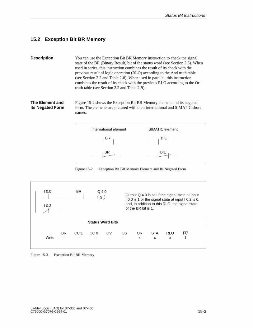
15-3Ladder Logic (LAD) for S7-300 and S7-400C79000-G7076-C564-01
15.2 Exception Bit BR Memory
You can use the Exception Bit BR Memory instruction to check the signalstate of the BR (Binary Result) bit of the status word (see Section 2.3). Whenused in series, this instruction combines the result of its check with theprevious result of logic operation (RLO) according to the And truth table(see Section 2.2 and Table 2-8). When used in parallel, this instructioncombines the result of its check with the previous RLO according to the Ortruth table (see Section 2.2 and Table 2-9).
Figure 15-2 shows the Exception Bit BR Memory element and its negatedform. The elements are pictured with their international and SIMATIC shortnames.
BR
BR
BIE
BIE
International element SIMATIC element
Figure 15-2 Exception Bit BR Memory Element and Its Negated Form
Status Word Bits
BR CC 1 CC 0 OV OS OR STA RLO FCWrite – – – – – x x x 1
I 0.0Output Q 4.0 is set if the signal state at inputI 0.0 is 1 or the signal state at input I 0.2 is 0,and, in addition to this RLO, the signal stateof the BR bit is 1.
BR Q 4.0
S
I 0.2
Figure 15-3 Exception Bit BR Memory
Description
The Element andIts Negated Form
Status Bit Instructions
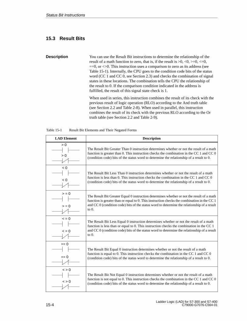
15-4Ladder Logic (LAD) for S7-300 and S7-400
C79000-G7076-C564-01
15.3 Result Bits
You can use the Result Bit instructions to determine the relationship of theresult of a math function to zero, that is, if the result is >0, <0, >=0, <=0,==0, or <>0. This instruction uses a comparison to zero as its address (seeTable 15-1). Internally, the CPU goes to the condition code bits of the statusword (CC 1 and CC 0, see Section 2.3) and checks the combination of signalstates in these locations. The combination tells the CPU the relationship ofthe result to 0. If the comparison condition indicated in the address isfulfilled, the result of this signal state check is 1.
When used in series, this instruction combines the result of its check with theprevious result of logic operation (RLO) according to the And truth table(see Section 2.2 and Table 2-8). When used in parallel, this instructioncombines the result of its check with the previous RLO according to the Ortruth table (see Section 2.2 and Table 2-9).
Table 15-1 Result Bit Elements and Their Negated Forms
LAD Element Description
> 0
> 0The Result Bit Greater Than 0 instruction determines whether or not the result of a mathfunction is greater than 0. This instruction checks the combination in the CC 1 and CC 0(condition code) bits of the status word to determine the relationship of a result to 0.
< 0
< 0
The Result Bit Less Than 0 instruction determines whether or not the result of a mathfunction is less than 0. This instruction checks the combination in the CC 1 and CC 0(condition code) bits of the status word to determine the relationship of a result to 0.
> = 0
> = 0
The Result Bit Greater Equal 0 instruction determines whether or not the result of a mathfunction is greater than or equal to 0. This instruction checks the combination in the CC 1and CC 0 (condition code) bits of the status word to determine the relationship of a resultto 0.
< = 0
< = 0
The Result Bit Less Equal 0 instruction determines whether or not the result of a mathfunction is less than or equal to 0. This instruction checks the combination in the CC 1and CC 0 (condition code) bits of the status word to determine the relationship of a resultto 0.
== 0
== 0
The Result Bit Equal 0 instruction determines whether or not the result of a mathfunction is equal to 0. This instruction checks the combination in the CC 1 and CC 0(condition code) bits of the status word to determine the relationship of a result to 0.
< > 0
< > 0
The Result Bit Not Equal 0 instruction determines whether or not the result of a mathfunction is not equal to 0. This instruction checks the combination in the CC 1 and CC 0(condition code) bits of the status word to determine the relationship of a result to 0.
Description
Status Bit Instructions
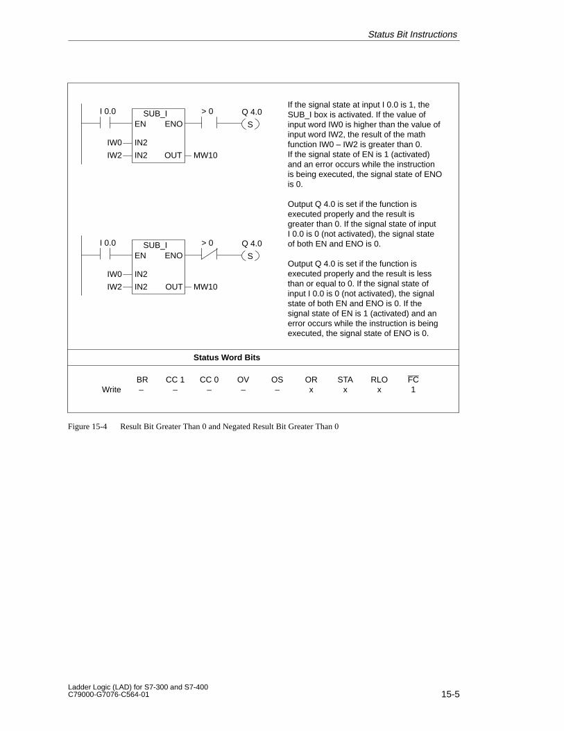
15-5Ladder Logic (LAD) for S7-300 and S7-400C79000-G7076-C564-01
Status Word Bits
BR CC 1 CC 0 OV OS OR STA RLO FCWrite – – – – – x x x 1
I 0.0If the signal state at input I 0.0 is 1, theSUB_I box is activated. If the value ofinput word IW0 is higher than the value ofinput word IW2, the result of the mathfunction IW0 – IW2 is greater than 0.If the signal state of EN is 1 (activated)and an error occurs while the instructionis being executed, the signal state of ENOis 0.
Output Q 4.0 is set if the function isexecuted properly and the result isgreater than 0. If the signal state of inputI 0.0 is 0 (not activated), the signal stateof both EN and ENO is 0.
Output Q 4.0 is set if the function isexecuted properly and the result is lessthan or equal to 0. If the signal state ofinput I 0.0 is 0 (not activated), the signalstate of both EN and ENO is 0. If thesignal state of EN is 1 (activated) and anerror occurs while the instruction is beingexecuted, the signal state of ENO is 0.
Q 4.0SUB_I
IN2
OUT
EN ENO
IN2
IW0
IW2 MW10
S
> 0
I 0.0 Q 4.0SUB_I
IN2
OUT
EN ENO
IN2
IW0
IW2 MW10
S
> 0
Figure 15-4 Result Bit Greater Than 0 and Negated Result Bit Greater Than 0
Status Bit Instructions
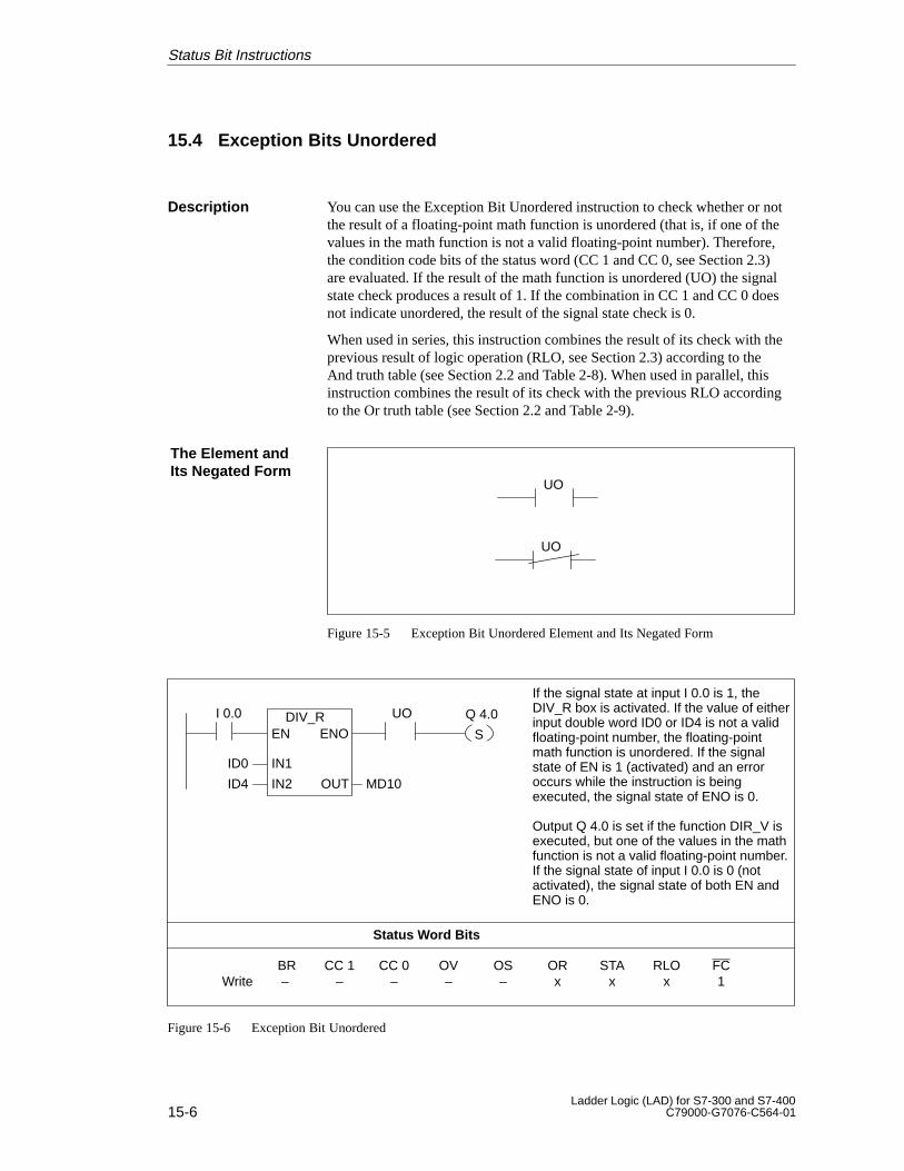
15-6Ladder Logic (LAD) for S7-300 and S7-400
C79000-G7076-C564-01
15.4 Exception Bits Unordered
You can use the Exception Bit Unordered instruction to check whether or notthe result of a floating-point math function is unordered (that is, if one of thevalues in the math function is not a valid floating-point number). Therefore,the condition code bits of the status word (CC 1 and CC 0, see Section 2.3)are evaluated. If the result of the math function is unordered (UO) the signalstate check produces a result of 1. If the combination in CC 1 and CC 0 doesnot indicate unordered, the result of the signal state check is 0.
When used in series, this instruction combines the result of its check with theprevious result of logic operation (RLO, see Section 2.3) according to theAnd truth table (see Section 2.2 and Table 2-8). When used in parallel, thisinstruction combines the result of its check with the previous RLO accordingto the Or truth table (see Section 2.2 and Table 2-9).
UO
UO
Figure 15-5 Exception Bit Unordered Element and Its Negated Form
Status Word Bits
BR CC 1 CC 0 OV OS OR STA RLO FCWrite – – – – – x x x 1
I 0.0
If the signal state at input I 0.0 is 1, theDIV_R box is activated. If the value of eitherinput double word ID0 or ID4 is not a validfloating-point number, the floating-pointmath function is unordered. If the signalstate of EN is 1 (activated) and an erroroccurs while the instruction is beingexecuted, the signal state of ENO is 0.
Output Q 4.0 is set if the function DIR_V isexecuted, but one of the values in the mathfunction is not a valid floating-point number.If the signal state of input I 0.0 is 0 (notactivated), the signal state of both EN andENO is 0.
DIV_R
IN1
OUT
EN ENO
IN2
ID0
ID4 MD10
UO Q 4.0
S
Figure 15-6 Exception Bit Unordered
Description
The Element andIts Negated Form
Status Bit Instructions
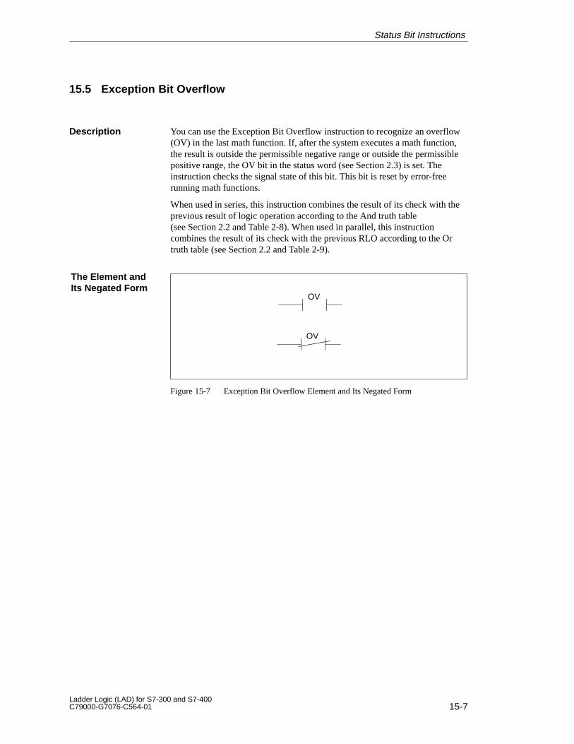
15-7Ladder Logic (LAD) for S7-300 and S7-400C79000-G7076-C564-01
15.5 Exception Bit Overflow
You can use the Exception Bit Overflow instruction to recognize an overflow(OV) in the last math function. If, after the system executes a math function,the result is outside the permissible negative range or outside the permissiblepositive range, the OV bit in the status word (see Section 2.3) is set. Theinstruction checks the signal state of this bit. This bit is reset by error-freerunning math functions.
When used in series, this instruction combines the result of its check with theprevious result of logic operation according to the And truth table(see Section 2.2 and Table 2-8). When used in parallel, this instructioncombines the result of its check with the previous RLO according to the Ortruth table (see Section 2.2 and Table 2-9).
OV
OV
Figure 15-7 Exception Bit Overflow Element and Its Negated Form
Description
The Element andIts Negated Form
Status Bit Instructions
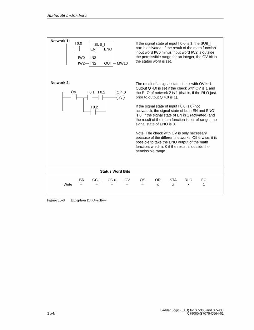
15-8Ladder Logic (LAD) for S7-300 and S7-400
C79000-G7076-C564-01
Status Word Bits
I 0.0 If the signal state at input I 0.0 is 1, the SUB_Ibox is activated. If the result of the math functioninput word IW0 minus input word IW2 is outsidethe permissible range for an integer, the OV bit inthe status word is set.
The result of a signal state check with OV is 1.Output Q 4.0 is set if the check with OV is 1 andthe RLO of network 2 is 1 (that is, if the RLO justprior to output Q 4.0 is 1).
If the signal state of input I 0.0 is 0 (notactivated), the signal state of both EN and ENOis 0. If the signal state of EN is 1 (activated) andthe result of the math function is out of range, thesignal state of ENO is 0.
Note: The check with OV is only necessarybecause of the different networks. Otherwise, it ispossible to take the ENO output of the mathfunction, which is 0 if the result is outside thepermissible range.
SUB_I
IN2
OUT
EN ENO
IN2
IW0
IW2 MW10
Network 1:
OV
Network 2:
I 0.1 I 0.2
I 0.2
Q 4.0
S
BR CC 1 CC 0 OV OS OR STA RLO FCWrite – – – – – x x x 1
Figure 15-8 Exception Bit Overflow
Status Bit Instructions
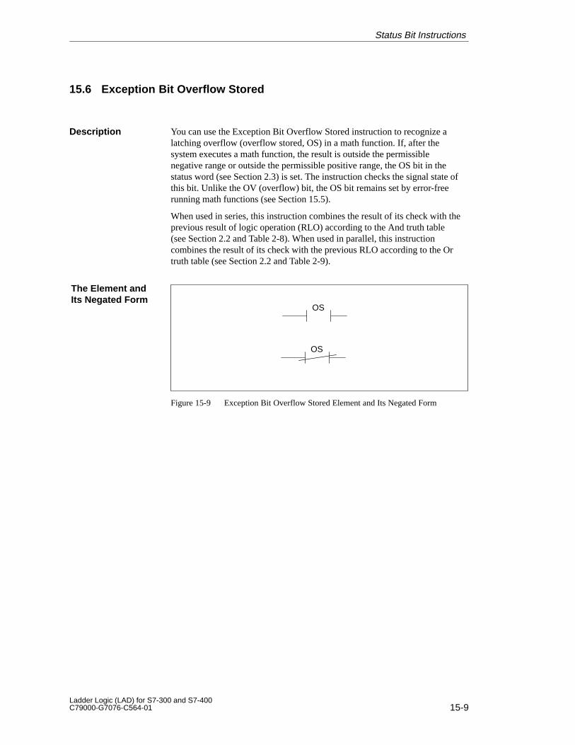
15-9Ladder Logic (LAD) for S7-300 and S7-400C79000-G7076-C564-01
15.6 Exception Bit Overflow Stored
You can use the Exception Bit Overflow Stored instruction to recognize alatching overflow (overflow stored, OS) in a math function. If, after thesystem executes a math function, the result is outside the permissiblenegative range or outside the permissible positive range, the OS bit in thestatus word (see Section 2.3) is set. The instruction checks the signal state ofthis bit. Unlike the OV (overflow) bit, the OS bit remains set by error-freerunning math functions (see Section 15.5).
When used in series, this instruction combines the result of its check with theprevious result of logic operation (RLO) according to the And truth table(see Section 2.2 and Table 2-8). When used in parallel, this instructioncombines the result of its check with the previous RLO according to the Ortruth table (see Section 2.2 and Table 2-9).
OS
OS
Figure 15-9 Exception Bit Overflow Stored Element and Its Negated Form
Description
The Element andIts Negated Form
Status Bit Instructions
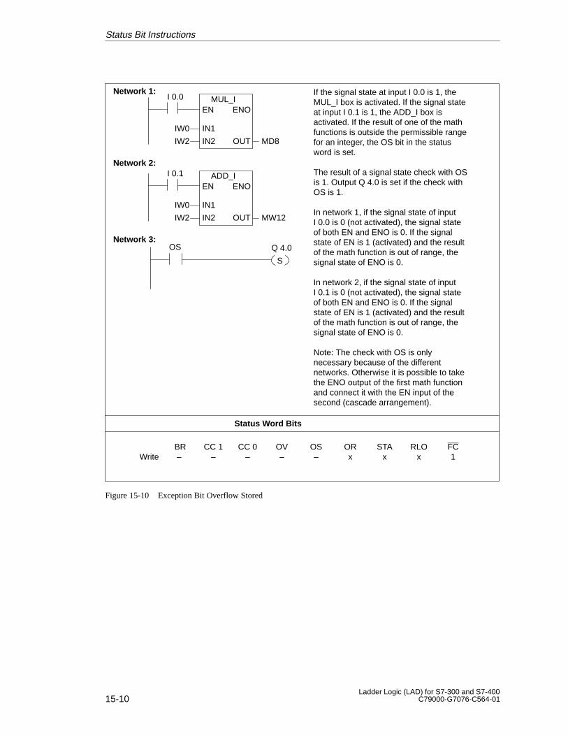
15-10Ladder Logic (LAD) for S7-300 and S7-400
C79000-G7076-C564-01
Status Word Bits
BR CC 1 CC 0 OV OS OR STA RLO FCWrite – – – – – x x x 1
I 0.0 If the signal state at input I 0.0 is 1, theMUL_I box is activated. If the signal stateat input I 0.1 is 1, the ADD_I box isactivated. If the result of one of the mathfunctions is outside the permissible rangefor an integer, the OS bit in the statusword is set.
The result of a signal state check with OSis 1. Output Q 4.0 is set if the check withOS is 1.
In network 1, if the signal state of inputI 0.0 is 0 (not activated), the signal stateof both EN and ENO is 0. If the signalstate of EN is 1 (activated) and the resultof the math function is out of range, thesignal state of ENO is 0.
In network 2, if the signal state of inputI 0.1 is 0 (not activated), the signal stateof both EN and ENO is 0. If the signalstate of EN is 1 (activated) and the resultof the math function is out of range, thesignal state of ENO is 0.
Note: The check with OS is onlynecessary because of the differentnetworks. Otherwise it is possible to takethe ENO output of the first math functionand connect it with the EN input of thesecond (cascade arrangement).
MUL_I
IN1
OUT
EN ENO
IN2
IW0
IW2 MD8
Network 1:
Network 2:
OSNetwork 3:
Q 4.0
S
I 0.1 ADD_I
IN1
OUT
EN ENO
IN2
IW0
IW2 MW12
Figure 15-10 Exception Bit Overflow Stored
Status Bit Instructions
16-1Ladder Logic (LAD) for S7-300 and S7-400C79000-G7076-C564-01
Program Control Instructions
Section Description Page
16.1 Calling FCs/SFCs from Coil 16-2
16.2 Calling FBs, FCs, SFBs, SFCs, and Multiple Instances 16-4
16.3 Return 16-8
16.4 Master Control Relay Instructions 16-10
16.5 Master Control Relay Activate/Deactivate 16-11
16.6 Master Control Relay On/Off 16-14
Chapter Overview
16

16-2Ladder Logic (LAD) for S7-300 and S7-400
C79000-G7076-C564-01
16.1 Calling FCs/SFCs from Coil
You can use the Call FC/SFC from Coil instruction to call a function (FC) ora system function (SFC) that has no parameters. Depending on the precedinglink, the call is conditional or unconditional (see the example in Figure 16-1).
In the case of a conditional call, you cannot enter parameters of data typeBLOCK_FC in the code section of a function (FC). Within a function block(FB), however, you can enter BLOCK_FC as a parameter type.
A conditional call is executed only if the RLO is 1. If a conditional call is notexecuted, the RLO after the call instruction is 0. If the instruction isexecuted, it performs the following functions:
� Saves the address that it needs to return to the calling block
� Saves the selectors of both current data blocks (DB and DI)
� Changes the current local data range to the previous local data range
� Pushes the MA bit (MCR Active bit) to the block stack (BSTACK)
� Creates the new local data range for the called FC or SFC
After all this, program processing continues in the called block. Forinformation on the passing of parameters, see the STEP 7 Online Help.
Table 16-1 Call FC/SFC from Coil Element and Parameter
LAD Element Parameter Data Type Memory Area Description
CALLNumber
Number BLOCK_FC –
Number of the FC or SFC (for example,FC10 or SFC59). The SFCs that areavailable depend on your CPU.
In the case of a conditional call, youcannot enter parameters of data typeBLOCK_FC within a function (FC).Within a function block, however, youcan enter BLOCK_FC as a parametertype.
Description
Program Control Instructions
16-3Ladder Logic (LAD) for S7-300 and S7-400C79000-G7076-C564-01
OPN
If the unconditional call of FC10 is executed, the CALL instruction performs the followingfunctions:
� Saves the address that it needs to return to the current FB� Saves the selectors for DB10 and for the instance data block of the FB� Pushes the MA bit, set to 1 in the MCRA instruction, to the block stack (BSTACK) and
resets this bit to 0 for the called FC10
Program processing continues in FC10. If you want to use the MCR function in FC10, you mustreactivate it there. When FC10 is finished, program processing returns to the calling FB. TheMA bit is restored, and DB10 and the instance data block of the user-defined FB are the currentDBs again, regardless of which DBs FC10 used.
After jumping back from FC10 the signal state of input I 0.0 is assigned to output Q 4.0. The callof FC11 is a conditional call. It is executed only if the signal state of input I 0.1 is 1. If the call isexecuted, the function is the same as for calling FC10.
I 0.0 Q 4.0
I 0.1 FC11
DB10
MCRA
CALLFC10
CALL
.
.
.
.
.
.
.
.
.
.
.
.
.
.
.
.
.
.
.
.
Status Word Bits
BR CC 1 CC 0 OV OS OR STA RLO FCWrite – – – – 0 0 1 – 0
MCRD
BR CC 1 CC 0 OV OS OR STA RLO FCWrite – – – – 0 0 1 1 0
Unconditional Call
Conditional Call
Figure 16-1 Call FC/SFC from Coil
Program Control Instructions
16-4Ladder Logic (LAD) for S7-300 and S7-400
C79000-G7076-C564-01
16.2 Calling FBs, FCs, SFBs, SFCs, and Multiple Instances
You can call function blocks (FBs), functions (FCs), system function blocks(SFBs), and system functions (SFCs), and multiple instances by selectingthem from the “Program Elements” list box. They are at the end of the list ofinstruction families under the following names:
� FB Blocks
� FC Blocks
� SFB Blocks
� SFC Blocks
� Multiple Instances
� Libraries
When you select one of these blocks, a box appears on your screen with thenumber or symbolic name of the function or function block and theparameters that belong to it.
The block that you call must have been compiled and must already exist inyour program file, in the library, or on the CPU.
If the call FB, FC, SFB, SFC, and multiple instances instruction is executed,it performs the following functions:
� Saves the address that it needs to return to the calling block
� Saves the selectors of both current data blocks (DB and DI)
� Changes the previous local data range to the current local data range
� Pushes the MA bit (MCR Active bit) to the block stack (BSTACK)
� Creates the new local data range for the called FC or SFC
Note
When the DB and DI registers are saved, they may not point to the datablocks that you opened. Because of the copy-in and copy-out mechanism forpassing parameters, especially where function blocks are concerned, thecompiler sometimes overwrites the DB register. See the STEP 7 Online Helpfor more details.
After this, program processing continues in the called block.
Description
Program Control Instructions
16-5Ladder Logic (LAD) for S7-300 and S7-400C79000-G7076-C564-01
The enable output (ENO) of a Ladder box corresponds to the BR bit of thestatus word (see Section 2.3). When writing a function block or function thatyou want to call from Ladder, no matter whether you write the FB or FC inSTL or Ladder, you are responsible for managing the BR bit. You should usethe SAVE instruction (in STL) or the –––(SAVE) coil (in Ladder) to store anRLO in the BR bit according to the following criteria:
� Store an RLO of 1 in the BR bit for a case where the FB or FC isexecuted without error.
� Store an RLO of 0 in the BR bit for a case where the FB or FC isexecuted with error
You should program these instructions at the end of the FB or FC so thatthese are the last instructions that are executed in the block.
!Warning
Possible unintentional resetting of the BR bit to 0.
When writing FBs and FCs in LAD, if you fail to manage the BR bit asdescribed above, one FB or FC may overwrite the BR bit of another FBor FC.
To avoid this problem, store the RLO at the end of each FB or FC asdescribed above.
Figure 16-2 shows the effects of a conditional and an unconditional call of ablock on the bits of the status word (see Section 2.3).
Conditional:Unconditional:
BR CC 1 CC 0 OV OS OR STA RLO FCWrite x – – – 0 0 1 1 xWrite – – – – 0 0 1 – x
Figure 16-2 Effect of a Block Call on the Bits of the Status Word
Enable Output
Effect of the Callon the Bits of theStatus Word
Program Control Instructions

16-6Ladder Logic (LAD) for S7-300 and S7-400
C79000-G7076-C564-01
The parameters that have been defined in the VAR section of the block willbe displayed in the ladder box. Supplying parameters differs depending onthe type of block as follows:
� For a function (FC), you must supply actual parameters for all of theformal parameters.
� The entry of actual parameters is optional with function blocks (FBs).You must, however, attach an instance data block (instance DB) to theFB. If an actual parameter has not been attached to a formal parameter,the FB works with the values that exist in its instance DB.
� With multiple instances, you do not need to specify the instance DB sincethe box that is called has already been assigned the DB number (for moreinformation about declaring multiple instances, refer to the STEP 7Online Help).
For structured IN/OUT parameters and parameters of the types “Pointer” and“Array”, you must make an actual parameter available (at least during thefirst call).
Every actual parameter that you make available when calling a functionblock must have the same data type as its formal parameter.
For information on how to program a function or how to work with itsparameters, see the STEP 7 Online Help.
Table 16-2 shows a box for calling FBs, FCs, SFBs, SFCs, and multipleinstances and describes the parameters common to the box for all theseblocks. When you call your block from the Instruction Browser, the blocknumber appears automatically at the top of the block (number of the FB, FC,SFB, or SFC, for example, FC10).
Table 16-2 Box and Parameters for Calling FBs, FCs, SFBs, SFCs, and Multiple Instances
LAD Box Parameter Data Type Memory Area Description
Block no.EN ENO
DB No.DB No. BLOCK_DB –
Instance data block number. You need tosupply this information for calling FBsonly.
EN ENO
IN OUT
IN/OUTEN BOOL I, Q, M, D, L Enable input
IN/OUTENO BOOL I, Q, M, D, L Enable output
Parameters
Program Control Instructions
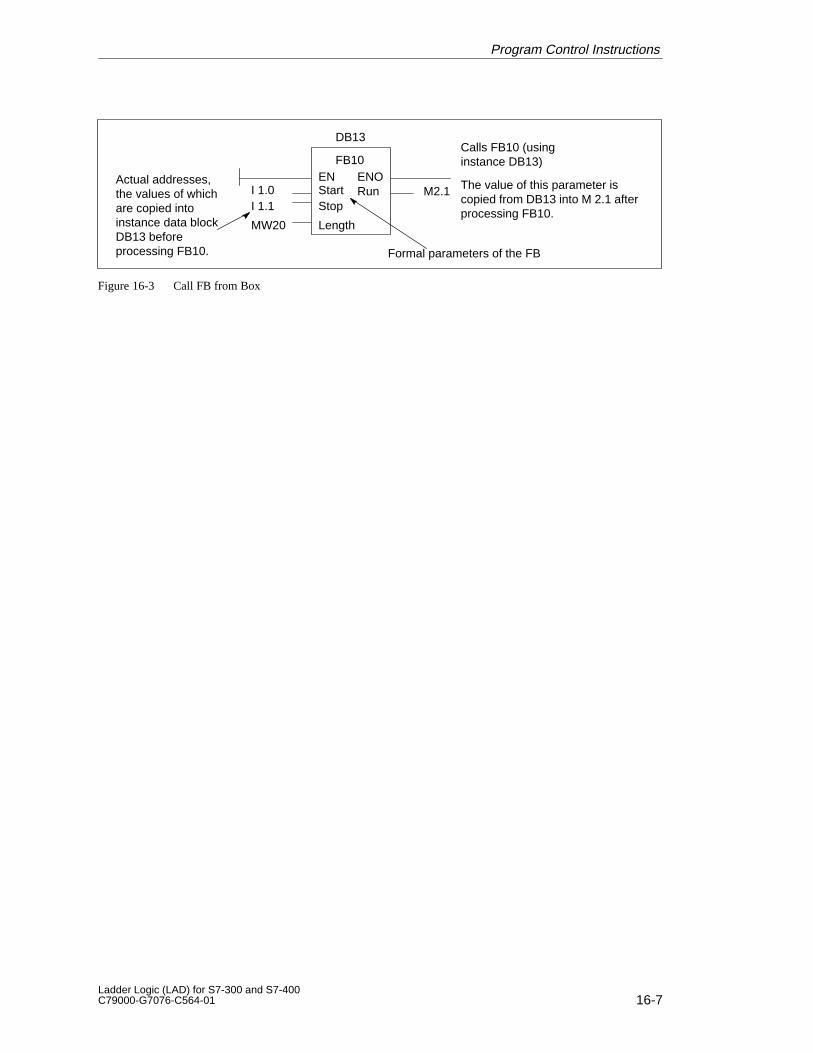
16-7Ladder Logic (LAD) for S7-300 and S7-400C79000-G7076-C564-01
DB13
ENStartStop
Length
RunENO
Calls FB10 (usinginstance DB13)
I 1.0I 1.1
MW20
M2.1
FB10
Actual addresses,the values of whichare copied intoinstance data blockDB13 beforeprocessing FB10. Formal parameters of the FB
The value of this parameter iscopied from DB13 into M 2.1 afterprocessing FB10.
Figure 16-3 Call FB from Box
Program Control Instructions
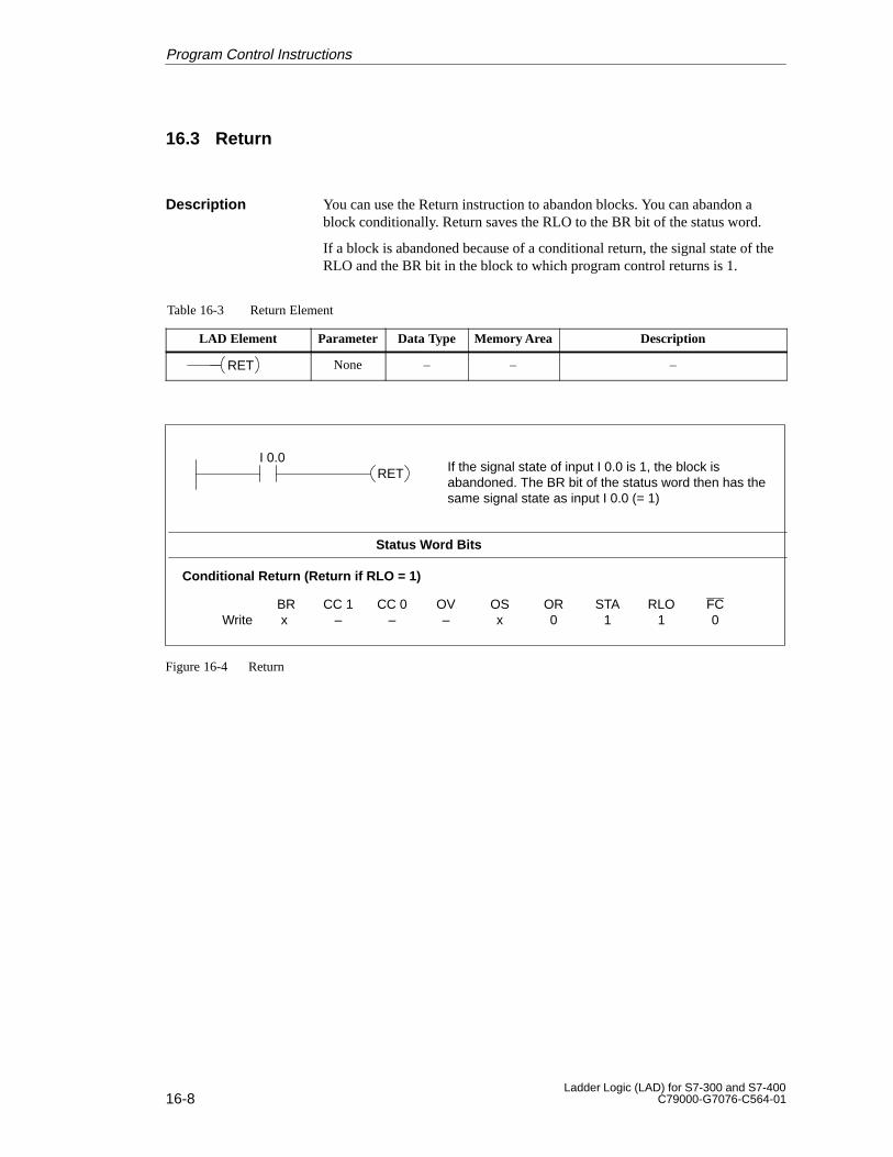
16-8Ladder Logic (LAD) for S7-300 and S7-400
C79000-G7076-C564-01
16.3 Return
You can use the Return instruction to abandon blocks. You can abandon ablock conditionally. Return saves the RLO to the BR bit of the status word.
If a block is abandoned because of a conditional return, the signal state of theRLO and the BR bit in the block to which program control returns is 1.
Table 16-3 Return Element
LAD Element Parameter Data Type Memory Area Description
RET None – – –
If the signal state of input I 0.0 is 1, the block isabandoned. The BR bit of the status word then has thesame signal state as input I 0.0 (= 1)
Status Word Bits
BR CC 1 CC 0 OV OS OR STA RLO FCWrite x – – – x 0 1 1 0
I 0.0RET
Conditional Return (Return if RLO = 1)
Figure 16-4 Return
Description
Program Control Instructions
16-9Ladder Logic (LAD) for S7-300 and S7-400C79000-G7076-C564-01
Important Notes on Using MCR Functions
Take care with blocks in which the Master Control Relay was activated withMCRA:
� If the MCR is deactivated, the value 0 is written by all assignments inprogram segments between (MCR<) and (MCR>).
� The MCR is deactivated if the RLO was =0 before an (MCR<) instruc-tion.
!Danger
PLC in STOP or undefined runtime characteristics!
The compiler also uses write access to local data behind the temporary varia-bles defined in VAR_TEMP for calculating addresses.
Formal parameter access
� Access to components of complex FC parameters of the type STRUCT,UDT, ARRAY, STRING
� Access to components of complex FB parameters of the type STRUCT,UDT, ARRAY, STRING from the IN_OUT area in a version 2 block.
� Access to parameters of a version 2 function block if its address isgreater than 8180.0.
� Access in a version 2 function block to a parameter of the typeBLOCK_DB opens DB0. Any subsequent data access sets the CPU toSTOP. T 0, C 0, FC0 or FB0 are always used for TIMER, COUNTER,BLOCK_FC, and BLOCK_FB.
Parameter passing
� Calls in which parameters are transferred.
KOP/FUP
� T branches and midline outputs in Ladder or FBD starting with RLO=0.
Remedy:
Free the above commands from their dependence on the MCR:
1. Deactivate the Master Control Relay using the Master Control RelayDeactivate instruction before the statement or network in question.
2. Activate the Master Control Relay again mit Master Control RelayActivate instruction after the statement or network in question.
Program Control Instructions
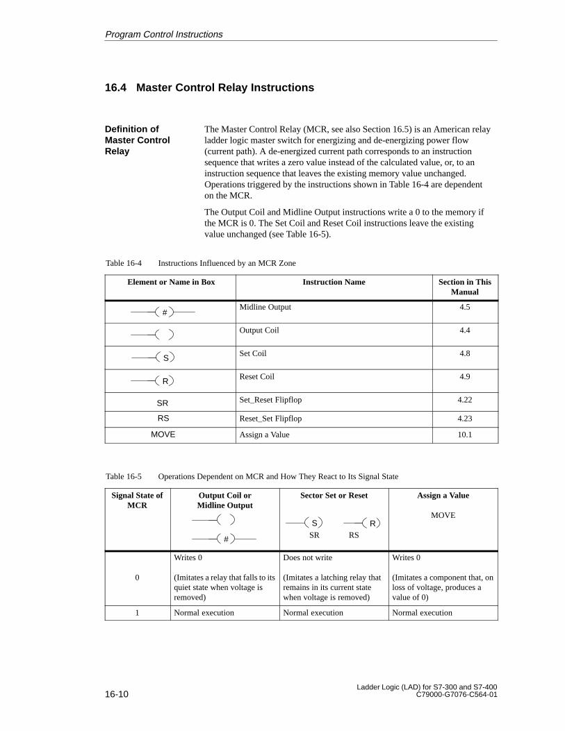
16-10Ladder Logic (LAD) for S7-300 and S7-400
C79000-G7076-C564-01
16.4 Master Control Relay Instructions
The Master Control Relay (MCR, see also Section 16.5) is an American relayladder logic master switch for energizing and de-energizing power flow(current path). A de-energized current path corresponds to an instructionsequence that writes a zero value instead of the calculated value, or, to aninstruction sequence that leaves the existing memory value unchanged.Operations triggered by the instructions shown in Table 16-4 are dependenton the MCR.
The Output Coil and Midline Output instructions write a 0 to the memory ifthe MCR is 0. The Set Coil and Reset Coil instructions leave the existingvalue unchanged (see Table 16-5).
Table 16-4 Instructions Influenced by an MCR Zone
Element or Name in Box Instruction Name Section in ThisManual
#Midline Output 4.5
Output Coil 4.4
SSet Coil 4.8
RReset Coil 4.9
SR Set_Reset Flipflop 4.22
RS Reset_Set Flipflop 4.23
MOVE Assign a Value 10.1
Table 16-5 Operations Dependent on MCR and How They React to Its Signal State
Signal State ofMCR
Output Coil orMidline Output
#
Sector Set or Reset
SR RS
S R
Assign a Value
MOVE
0
Writes 0
(Imitates a relay that falls to itsquiet state when voltage isremoved)
Does not write
(Imitates a latching relay thatremains in its current statewhen voltage is removed)
Writes 0
(Imitates a component that, onloss of voltage, produces avalue of 0)
1 Normal execution Normal execution Normal execution
Definition ofMaster ControlRelay
Program Control Instructions
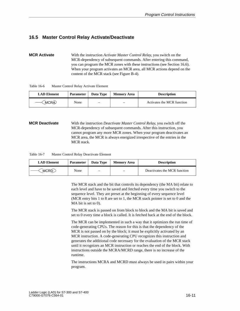
16-11Ladder Logic (LAD) for S7-300 and S7-400C79000-G7076-C564-01
16.5 Master Control Relay Activate/Deactivate
With the instruction Activate Master Control Relay, you switch on theMCR-dependency of subsequent commands. After entering this command,you can program the MCR zones with these instructions (see Section 16.6).When your program activates an MCR area, all MCR actions depend on thecontent of the MCR stack (see Figure B-4).
Table 16-6 Master Control Relay Activate Element
LAD Element Parameter Data Type Memory Area Description
MCRA None – – Activates the MCR function
With the instruction Deactivate Master Control Relay, you switch off theMCR-dependency of subsequent commands. After this instruction, youcannot program any more MCR zones. When your program deactivates anMCR area, the MCR is always energized irrespective of the entries in theMCR stack.
Table 16-7 Master Control Relay Deactivate Element
LAD Element Parameter Data Type Memory Area Description
MCRD None – – Deactivates the MCR function
The MCR stack and the bit that controls its dependency (the MA bit) relate toeach level and have to be saved and fetched every time you switch to thesequence level. They are preset at the beginning of every sequence level(MCR entry bits 1 to 8 are set to 1, the MCR stack pointer is set to 0 and theMA bit is set to 0).
The MCR stack is passed on from block to block and the MA bit is saved andset to 0 every time a block is called. It is fetched back at the end of the block.
The MCR can be implemented in such a way that it optimizes the run time ofcode-generating CPUs. The reason for this is that the dependency of theMCR is not passed on by the block; it must be explicitly activated by anMCR instruction. A code-generating CPU recognizes this instruction andgenerates the additional code necessary for the evaluation of the MCR stackuntil it recognizes an MCR instruction or reaches the end of the block. Withinstructions outside the MCRA/MCRD range, there is no increase of theruntime.
The instructions MCRA and MCRD must always be used in pairs within yourprogram.
MCR Activate
MCR Deactivate
Program Control Instructions
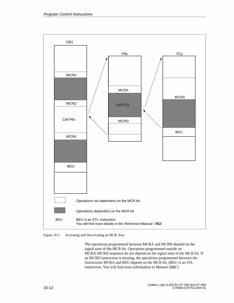
16-12Ladder Logic (LAD) for S7-300 and S7-400
C79000-G7076-C564-01
ÀÀÀÀÀÀÀÀÀÀÀÀÀÀÀÀÀÀÀÀÀÀÀÀÀÀÀÀÀÀÀÀÀÀÀÀ
ÀÀÀÀÀÀÀÀÀÀÀÀÀÀÀÀÀÀÀÀÀÀÀÀÀÀÀÀÀÀ
ÀÀÀÀÀÀÀÀÀÀÀÀÀÀÀÀÀÀÀÀÀÀÀÀÀÀÀÀÀÀÀÀÀÀÀÀ
ÀÀÀÀÀÀÀÀÀÀÀÀÀÀÀÀÀÀ
ÀÀÀÀÀÀÀÀÀÀÀÀÀÀÀÀÀÀÀÀÀÀÀÀÀÀÀÀÀÀÀÀÀÀÀ
OB1
MCRA
MCRD
MCRA
MCRA
MCRA
MCRD
BEU
BEU
Operations dependent on the MCR bit
Operations not dependent on the MCR bit
Call FBx
FBx FCy
Call FCy
BEU BEU is an STL instruction. You will find more details in the Reference Manual /102/
Figure 16-5 Activating and Deactivating an MCR Area
The operations programmed between MCRA and MCRD depend on thesignal state of the MCR bit. Operations programmed outside anMCRA-MCRD sequence do not depend on the signal state of the MCR bit. Ifan MCRD instruction is missing, the operations programmed between theinstructions MCRA and BEU depend on the MCR bit. (BEU is an STLinstruction. You will find more information in Manual /232/.)
Program Control Instructions
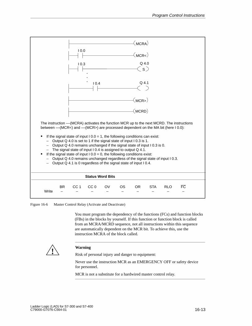
16-13Ladder Logic (LAD) for S7-300 and S7-400C79000-G7076-C564-01
The instruction ––(MCRA) activates the function MCR up to the next MCRD. The instructionsbetween ––(MCR<) and ––(MCR>) are processed dependent on the MA bit (here I 0.0): � If the signal state of input I 0.0 = 1, the following conditions can exist:
– Output Q 4.0 is set to 1 if the signal state of input I 0.3 is 1.– Output Q 4.0 remains unchanged if the signal state of input I 0.3 is 0.– The signal state of input I 0.4 is assigned to output Q 4.1.
� If the signal state of input I 0.0 = 0, the following conditions exist:– Output Q 4.0 remains unchanged regardless of the signal state of input I 0.3.– Output Q 4.1 is 0 regardless of the signal state of input I 0.4.
S
I 0.3 Q 4.0
I 0.4 Q 4.1
.
.
.
MCRA
MCR<I 0.0
MCR>
MCRD
Status Word Bits
BR CC 1 CC 0 OV OS OR STA RLO FCWrite – – – – – – – – –
Figure 16-6 Master Control Relay (Activate and Deactivate)
You must program the dependency of the functions (FCs) and function blocks(FBs) in the blocks by yourself. If this function or function block is calledfrom an MCRA/MCRD sequence, not all instructions within this sequenceare automatically dependent on the MCR bit. To achieve this, use theinstruction MCRA of the block called.
!Warning
Risk of personal injury and danger to equipment:
Never use the instruction MCR as an EMERGENCY OFF or safety devicefor personnel.
MCR is not a substitute for a hardwired master control relay.
Program Control Instructions
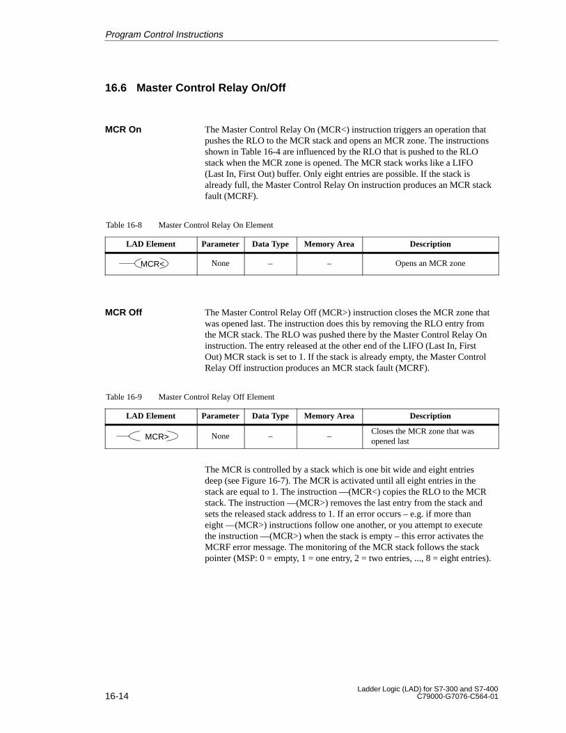
16-14Ladder Logic (LAD) for S7-300 and S7-400
C79000-G7076-C564-01
16.6 Master Control Relay On/Off
The Master Control Relay On (MCR<) instruction triggers an operation thatpushes the RLO to the MCR stack and opens an MCR zone. The instructionsshown in Table 16-4 are influenced by the RLO that is pushed to the RLOstack when the MCR zone is opened. The MCR stack works like a LIFO(Last In, First Out) buffer. Only eight entries are possible. If the stack isalready full, the Master Control Relay On instruction produces an MCR stackfault (MCRF).
Table 16-8 Master Control Relay On Element
LAD Element Parameter Data Type Memory Area Description
MCR< None – – Opens an MCR zone
The Master Control Relay Off (MCR>) instruction closes the MCR zone thatwas opened last. The instruction does this by removing the RLO entry fromthe MCR stack. The RLO was pushed there by the Master Control Relay Oninstruction. The entry released at the other end of the LIFO (Last In, FirstOut) MCR stack is set to 1. If the stack is already empty, the Master ControlRelay Off instruction produces an MCR stack fault (MCRF).
Table 16-9 Master Control Relay Off Element
LAD Element Parameter Data Type Memory Area Description
MCR> None – –Closes the MCR zone that wasopened last
The MCR is controlled by a stack which is one bit wide and eight entriesdeep (see Figure 16-7). The MCR is activated until all eight entries in thestack are equal to 1. The instruction ––(MCR<) copies the RLO to the MCRstack. The instruction ––(MCR>) removes the last entry from the stack andsets the released stack address to 1. If an error occurs – e.g. if more thaneight ––(MCR>) instructions follow one another, or you attempt to executethe instruction ––(MCR>) when the stack is empty – this error activates theMCRF error message. The monitoring of the MCR stack follows the stackpointer (MSP: 0 = empty, 1 = one entry, 2 = two entries, ..., 8 = eight entries).
MCR On
MCR Off
Program Control Instructions
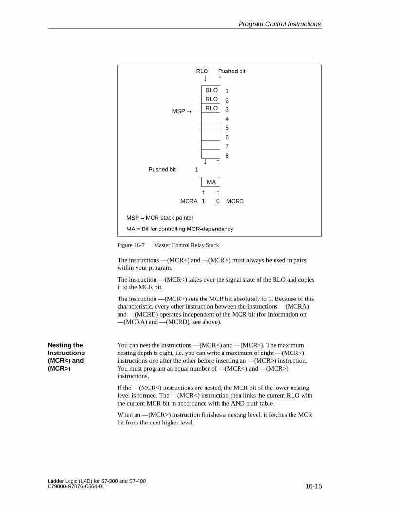
16-15Ladder Logic (LAD) for S7-300 and S7-400C79000-G7076-C564-01
RLO
RLO
RLOMSP �
MA
MCRA MCRD1 0
� �
1
2
3
4
5
6
7
8
RLO Pushed bit� �
� �
MSP = MCR stack pointer
MA = Bit for controlling MCR-dependency
Pushed bit 1
Figure 16-7 Master Control Relay Stack
The instructions ––(MCR<) and ––(MCR>) must always be used in pairswithin your program.
The instruction ––(MCR<) takes over the signal state of the RLO and copiesit to the MCR bit.
The instruction ––(MCR>) sets the MCR bit absolutely to 1. Because of thischaracteristic, every other instruction between the instructions ––(MCRA)and ––(MCRD) operates independent of the MCR bit (for information on––(MCRA) and ––(MCRD), see above).
You can nest the instructions ––(MCR<) and ––(MCR>). The maximumnesting depth is eight, i.e. you can write a maximum of eight ––(MCR<)instructions one after the other before inserting an ––(MCR>) instruction.You must program an equal number of ––(MCR<) and ––(MCR>)instructions.
If the ––(MCR<) instructions are nested, the MCR bit of the lower nestinglevel is formed. The ––(MCR<) instruction then links the current RLO withthe current MCR bit in accordance with the AND truth table.
When an ––(MCR>) instruction finishes a nesting level, it fetches the MCRbit from the next higher level.
Nesting theInstructions(MCR<) and(MCR>)
Program Control Instructions
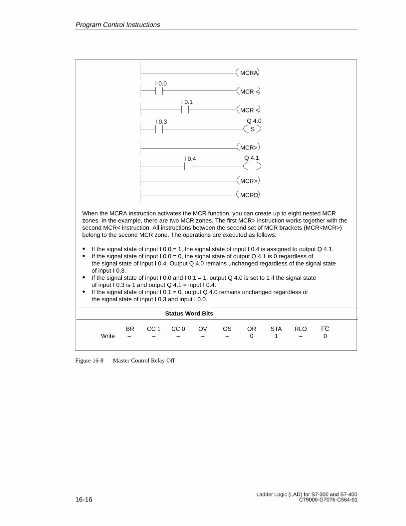
16-16Ladder Logic (LAD) for S7-300 and S7-400
C79000-G7076-C564-01
When the MCRA instruction activates the MCR function, you can create up to eight nested MCRzones. In the example, there are two MCR zones. The first MCR> instruction works together with thesecond MCR< instruction. All instructions between the second set of MCR brackets (MCR<MCR>)belong to the second MCR zone. The operations are executed as follows:
� If the signal state of input I 0.0 = 1, the signal state of input I 0.4 is assigned to output Q 4.1.� If the signal state of input I 0.0 = 0, the signal state of output Q 4.1 is 0 regardless of
the signal state of input I 0.4. Output Q 4.0 remains unchanged regardless of the signal stateof input I 0.3.
� If the signal state of input I 0.0 and I 0.1 = 1, output Q 4.0 is set to 1 if the signal stateof input I 0.3 is 1 and output Q 4.1 = input I 0.4.
� If the signal state of input I 0.1 = 0, output Q 4.0 remains unchanged regardless ofthe signal state of input I 0.3 and input I 0.0.
I 0.0
I 0.1
I 0.3 Q 4.0
Status Word Bits
BR CC 1 CC 0 OV OS OR STA RLO FCWrite – – – – – 0 1 – 0
S
I 0.4
MCR>
MCRD
MCR <
MCRA
MCR>
Q 4.1
MCR <
Figure 16-8 Master Control Relay Off
Program Control Instructions

Alphabetical Listing ofInstructions A
Programming Examples B
References C
Appendix

P-18Ladder Logic (LAD) for S7-300 and S7-400
C79000-G7076-C564-01
A-1Ladder Logic (LAD) for S7-300 and S7-400C79000-G7076-C564-01
Alphabetical Listing of Instructions
Section Description Page
A.1 Listing with International Names A-2
A.2 Listing with International Names and SIMATIC Equivalents A-5
A.3 Listing with SIMATIC Names A-9
A.4 Listing with SIMATIC Names and International Equivalents A-12
A.5 Listing with International Short Names and SIMATIC ShortNames
A-16
Chapter Overview
A
A-2Ladder Logic (LAD) for S7-300 and S7-400
C79000-G7076-C564-01
A.1 Listing with International Names
Table A-1 provides an alphabetical listing of instructions with internationalfull names. Next to each full name is its international short name and areference to the page on which the instruction is explained in this manual.
Table A-1 Ladder Logic Instructions Arranged Alphabetically by International Name, with Short Names
Full Name Short Name Page No.
Add Double Integer ADD_DI 7-3
Add Integer ADD_I 7-2
Add Real ADD_R 8-3
Address Negative Edge Detection NEG 4-22
Address Positive Edge Detection POS 4-21
Assign a Value MOVE 10-2
BCD to Double Integer BCD_DI 10-7
BCD to Integer BCD_I 10-4
Call FB from Box CALL_FB 16-4
Call FC from Box CALL_FC 16-4
Call FC SFC from Coil (without parameters) ––––(CALL) 16-2
Call System FB from Box CALL_SFB 16-4
Call System FC from Box CALL_SFC 16-4
Ceiling CEIL 10-17
Compare Double Integer (>, <, ==, <>, <=, >=) CMP>=D 9-3
Compare Integer (>, <, ==, <>, <=, >=) CMP>=I 9-2
Compare Real (>, <, ==, <>, <=, >=) CMP>=R 9-5
Divide Double Integer DIV_DI 7-9
Divide Integer DIV_I 7-8
Divide Real DIV_R 8-6
Double Integer to BCD DI_BCD 10-8
Double Integer to Real DI_R 10-9
Down Counter S_CD 6-7
Down Counter Coil ––––( CD ) 4-13
Exception Bit BR Memory BR –––| |––– 15-3
Exception Bit Overflow OV –––| |––– 15-7
Exception Bit Overflow Stored OS –––| |––– 15-9
Exception Bit Unordered UO –––| |––– 15-6
Extended Pulse S5 Timer S_PEXT 5-7
Extended Pulse Timer Coil –––( SE ) 4-15
Floor FLOOR 10-18
Integer to BCD I_BCD 10-5
Integer to Double Integer I_DI 10-6
Invert Power Flow –––| NOT |––– 4-7
Alphabetical Listing of Instructions
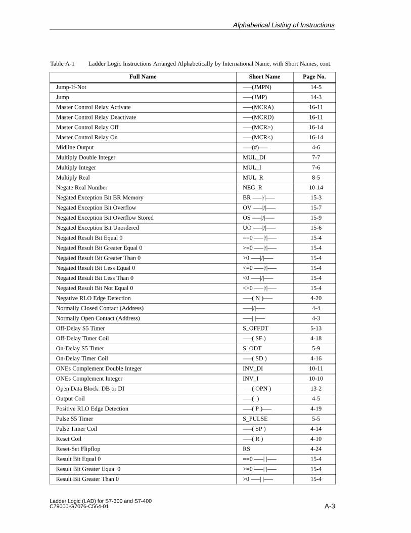
A-3Ladder Logic (LAD) for S7-300 and S7-400C79000-G7076-C564-01
Table A-1 Ladder Logic Instructions Arranged Alphabetically by International Name, with Short Names, cont.
Full Name Page No.Short Name
Jump-If-Not –––(JMPN) 14-5
Jump –––(JMP) 14-3
Master Control Relay Activate –––(MCRA) 16-11
Master Control Relay Deactivate –––(MCRD) 16-11
Master Control Relay Off –––(MCR>) 16-14
Master Control Relay On –––(MCR<) 16-14
Midline Output –––(#)––– 4-6
Multiply Double Integer MUL_DI 7-7
Multiply Integer MUL_I 7-6
Multiply Real MUL_R 8-5
Negate Real Number NEG_R 10-14
Negated Exception Bit BR Memory BR –––|/|––– 15-3
Negated Exception Bit Overflow OV –––|/|––– 15-7
Negated Exception Bit Overflow Stored OS –––|/|––– 15-9
Negated Exception Bit Unordered UO –––|/|––– 15-6
Negated Result Bit Equal 0 ==0 –––|/|––– 15-4
Negated Result Bit Greater Equal 0 >=0 –––|/|––– 15-4
Negated Result Bit Greater Than 0 >0 –––|/|––– 15-4
Negated Result Bit Less Equal 0 <=0 –––|/|––– 15-4
Negated Result Bit Less Than 0 <0 –––|/|––– 15-4
Negated Result Bit Not Equal 0 <>0 –––|/|––– 15-4
Negative RLO Edge Detection –––( N )––– 4-20
Normally Closed Contact (Address) –––|/|––– 4-4
Normally Open Contact (Address) –––| |––– 4-3
Off-Delay S5 Timer S_OFFDT 5-13
Off-Delay Timer Coil –––( SF ) 4-18
On-Delay S5 Timer S_ODT 5-9
On-Delay Timer Coil –––( SD ) 4-16
ONEs Complement Double Integer INV_DI 10-11
ONEs Complement Integer INV_I 10-10
Open Data Block: DB or DI –––( OPN ) 13-2
Output Coil –––( ) 4-5
Positive RLO Edge Detection –––( P )––– 4-19
Pulse S5 Timer S_PULSE 5-5
Pulse Timer Coil –––( SP ) 4-14
Reset Coil –––( R ) 4-10
Reset-Set Flipflop RS 4-24
Result Bit Equal 0 ==0 –––| |––– 15-4
Result Bit Greater Equal 0 >=0 –––| |––– 15-4
Result Bit Greater Than 0 >0 –––| |––– 15-4
Alphabetical Listing of Instructions
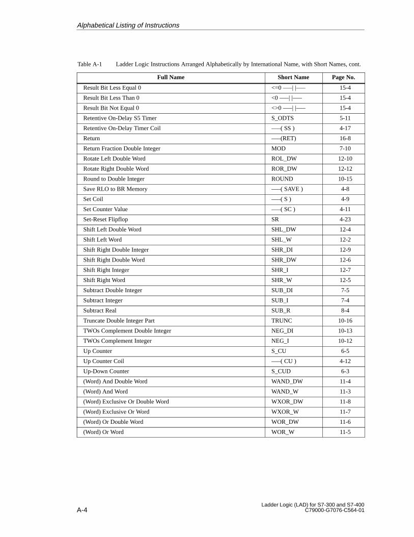
A-4Ladder Logic (LAD) for S7-300 and S7-400
C79000-G7076-C564-01
Table A-1 Ladder Logic Instructions Arranged Alphabetically by International Name, with Short Names, cont.
Full Name Page No.Short Name
Result Bit Less Equal 0 <=0 –––| |––– 15-4
Result Bit Less Than 0 <0 –––| |––– 15-4
Result Bit Not Equal 0 <>0 –––| |––– 15-4
Retentive On-Delay S5 Timer S_ODTS 5-11
Retentive On-Delay Timer Coil –––( SS ) 4-17
Return –––(RET) 16-8
Return Fraction Double Integer MOD 7-10
Rotate Left Double Word ROL_DW 12-10
Rotate Right Double Word ROR_DW 12-12
Round to Double Integer ROUND 10-15
Save RLO to BR Memory –––( SAVE ) 4-8
Set Coil –––( S ) 4-9
Set Counter Value –––( SC ) 4-11
Set-Reset Flipflop SR 4-23
Shift Left Double Word SHL_DW 12-4
Shift Left Word SHL_W 12-2
Shift Right Double Integer SHR_DI 12-9
Shift Right Double Word SHR_DW 12-6
Shift Right Integer SHR_I 12-7
Shift Right Word SHR_W 12-5
Subtract Double Integer SUB_DI 7-5
Subtract Integer SUB_I 7-4
Subtract Real SUB_R 8-4
Truncate Double Integer Part TRUNC 10-16
TWOs Complement Double Integer NEG_DI 10-13
TWOs Complement Integer NEG_I 10-12
Up Counter S_CU 6-5
Up Counter Coil –––( CU ) 4-12
Up-Down Counter S_CUD 6-3
(Word) And Double Word WAND_DW 11-4
(Word) And Word WAND_W 11-3
(Word) Exclusive Or Double Word WXOR_DW 11-8
(Word) Exclusive Or Word WXOR_W 11-7
(Word) Or Double Word WOR_DW 11-6
(Word) Or Word WOR_W 11-5
Alphabetical Listing of Instructions
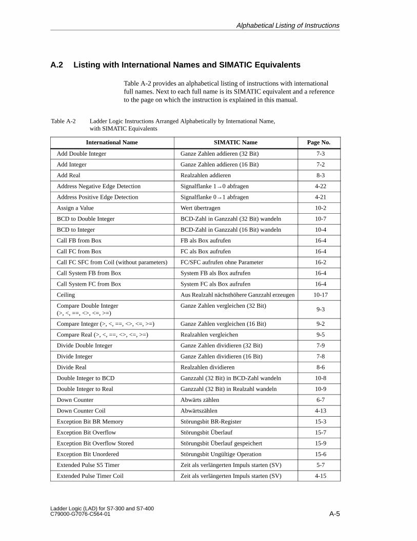
A-5Ladder Logic (LAD) for S7-300 and S7-400C79000-G7076-C564-01
A.2 Listing with International Names and SIMATIC Equivalents
Table A-2 provides an alphabetical listing of instructions with internationalfull names. Next to each full name is its SIMATIC equivalent and a referenceto the page on which the instruction is explained in this manual.
Table A-2 Ladder Logic Instructions Arranged Alphabetically by International Name,with SIMATIC Equivalents
International Name SIMATIC Name Page No.
Add Double Integer Ganze Zahlen addieren (32 Bit) 7-3
Add Integer Ganze Zahlen addieren (16 Bit) 7-2
Add Real Realzahlen addieren 8-3
Address Negative Edge Detection Signalflanke 1→0 abfragen 4-22
Address Positive Edge Detection Signalflanke 0→1 abfragen 4-21
Assign a Value Wert übertragen 10-2
BCD to Double Integer BCD-Zahl in Ganzzahl (32 Bit) wandeln 10-7
BCD to Integer BCD-Zahl in Ganzzahl (16 Bit) wandeln 10-4
Call FB from Box FB als Box aufrufen 16-4
Call FC from Box FC als Box aufrufen 16-4
Call FC SFC from Coil (without parameters) FC/SFC aufrufen ohne Parameter 16-2
Call System FB from Box System FB als Box aufrufen 16-4
Call System FC from Box System FC als Box aufrufen 16-4
Ceiling Aus Realzahl nächsthöhere Ganzzahl erzeugen 10-17
Compare Double Integer(>, <, ==, <>, <=, >=)
Ganze Zahlen vergleichen (32 Bit)9-3
Compare Integer (>, <, ==, <>, <=, >=) Ganze Zahlen vergleichen (16 Bit) 9-2
Compare Real (>, <, ==, <>, <=, >=) Realzahlen vergleichen 9-5
Divide Double Integer Ganze Zahlen dividieren (32 Bit) 7-9
Divide Integer Ganze Zahlen dividieren (16 Bit) 7-8
Divide Real Realzahlen dividieren 8-6
Double Integer to BCD Ganzzahl (32 Bit) in BCD-Zahl wandeln 10-8
Double Integer to Real Ganzzahl (32 Bit) in Realzahl wandeln 10-9
Down Counter Abwärts zählen 6-7
Down Counter Coil Abwärtszählen 4-13
Exception Bit BR Memory Störungsbit BR-Register 15-3
Exception Bit Overflow Störungsbit Überlauf 15-7
Exception Bit Overflow Stored Störungsbit Überlauf gespeichert 15-9
Exception Bit Unordered Störungsbit Ungültige Operation 15-6
Extended Pulse S5 Timer Zeit als verlängerten Impuls starten (SV) 5-7
Extended Pulse Timer Coil Zeit als verlängerten Impuls starten (SV) 4-15
Alphabetical Listing of Instructions
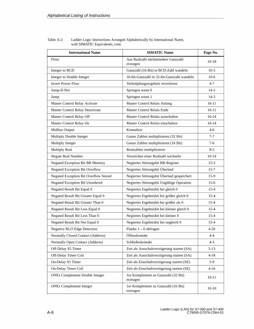
A-6Ladder Logic (LAD) for S7-300 and S7-400
C79000-G7076-C564-01
Table A-2 Ladder Logic Instructions Arranged Alphabetically by International Name,with SIMATIC Equivalents, cont.
International Name Page No.SIMATIC Name
Floor Aus Realzahl nächstniedere Ganzzahlerzeugen
10-18
Integer to BCD Ganzzahl (16 Bit) in BCD-Zahl wandeln 10-5
Integer to Double Integer 16-bit-Ganzzahl in 32-bit-Ganzzahl wandeln 10-6
Invert Power Flow Verknüpfungsergebnis invertieren 4-7
Jump-If-Not Springen wenn 0 14-5
Jump Springen wenn 1 14-3
Master Control Relay Activate Master Control Relais Anfang 16-11
Master Control Relay Deactivate Master Control Relais Ende 16-11
Master Control Relay Off Master Control Relais ausschalten 16-14
Master Control Relay On Master Control Relais einschalten 16-14
Midline Output Konnektor 4-6
Multiply Double Integer Ganze Zahlen multiplizieren (32 Bit) 7-7
Multiply Integer Ganze Zahlen multiplizieren (16 Bit) 7-6
Multiply Real Realzahlen multiplizieren 8-5
Negate Real Number Vorzeichen einer Realzahl wechseln 10-14
Negated Exception Bit BR Memory Negiertes Störungsbit BR-Register 15-3
Negated Exception Bit Overflow Negiertes Störungsbit Überlauf 15-7
Negated Exception Bit Overflow Stored Negiertes Störungsbit Überlauf gespeichert 15-9
Negated Exception Bit Unordered Negiertes Störungsbit Ungültige Operation 15-6
Negated Result Bit Equal 0 Negiertes Ergebnisbit bei gleich 0 15-4
Negated Result Bit Greater Equal 0 Negiertes Ergebnisbit bei größer gleich 0 15-4
Negated Result Bit Greater Than 0 Negiertes Ergebnisbit bei größer als 0 15-4
Negated Result Bit Less Equal 0 Negiertes Ergebnisbit bei kleiner gleich 0 15-4
Negated Result Bit Less Than 0 Negiertes Ergebnisbit bei kleiner 0 15-4
Negated Result Bit Not Equal 0 Negiertes Ergebnisbit bei ungleich 0 15-4
Negative RLO Edge Detection Flanke 1→0 abfragen 4-20
Normally Closed Contact (Address) Öffnerkontakt 4-4
Normally Open Contact (Address) Schließerkontakt 4-3
Off-Delay S5 Timer Zeit als Ausschaltverzögerung starten (SA) 5-13
Off-Delay Timer Coil Zeit als Ausschaltverzögerung starten (SA) 4-18
On-Delay S5 Timer Zeit als Einschaltverzögerung starten (SE) 5-9
On-Delay Timer Coil Zeit als Einschaltverzögerung starten (SE) 4-16
ONEs Complement Double Integer 1er Komplement zu Ganzzahl (32 Bit)erzeugen
10-11
ONEs Complement Integer 1er Komplement zu Ganzzahl (16 Bit)erzeugen
10-10
Alphabetical Listing of Instructions
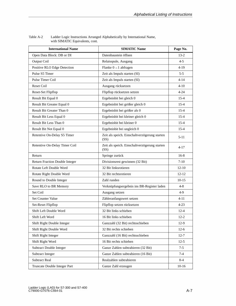
A-7Ladder Logic (LAD) for S7-300 and S7-400C79000-G7076-C564-01
Table A-2 Ladder Logic Instructions Arranged Alphabetically by International Name,with SIMATIC Equivalents, cont.
International Name Page No.SIMATIC Name
Open Data Block: DB or DI Datenbaustein öffnen 13-2
Output Coil Relaisspule, Ausgang 4-5
Positive RLO Edge Detection Flanke 0→1 abfragen 4-19
Pulse S5 Timer Zeit als Impuls starten (SI) 5-5
Pulse Timer Coil Zeit als Impuls starten (SI) 4-14
Reset Coil Ausgang rücksetzen 4-10
Reset-Set Flipflop Flipflop rücksetzen setzen 4-24
Result Bit Equal 0 Ergebnisbit bei gleich 0 15-4
Result Bit Greater Equal 0 Ergebnisbit bei größer gleich 0 15-4
Result Bit Greater Than 0 Ergebnisbit bei größer als 0 15-4
Result Bit Less Equal 0 Ergebnisbit bei kleiner gleich 0 15-4
Result Bit Less Than 0 Ergebnisbit bei kleiner 0 15-4
Result Bit Not Equal 0 Ergebnisbit bei ungleich 0 15-4
Retentive On-Delay S5 Timer Zeit als speich. Einschaltverzögerung starten(SS)
5-11
Retentive On-Delay Timer Coil Zeit als speich. Einschaltverzögerung starten(SS)
4-17
Return Springe zurück 16-8
Return Fraction Double Integer Divisionsrest gewinnen (32 Bit) 7-10
Rotate Left Double Word 32 Bit linksrotieren 12-10
Rotate Right Double Word 32 Bit rechtsrotieren 12-12
Round to Double Integer Zahl runden 10-15
Save RLO to BR Memory Verknüpfungsergebnis ins BR-Register laden 4-8
Set Coil Ausgang setzen 4-9
Set Counter Value Zähleranfangswert setzen 4-11
Set-Reset Flipflop Flipflop setzen rücksetzen 4-23
Shift Left Double Word 32 Bit links schieben 12-4
Shift Left Word 16 Bit links schieben 12-2
Shift Right Double Integer Ganzzahl (32 Bit) rechtsschieben 12-9
Shift Right Double Word 32 Bit rechts schieben 12-6
Shift Right Integer Ganzzahl (16 Bit) rechtsschieben 12-7
Shift Right Word 16 Bit rechts schieben 12-5
Subtract Double Integer Ganze Zahlen subtrahieren (32 Bit) 7-5
Subtract Integer Ganze Zahlen subtrahieren (16 Bit) 7-4
Subtract Real Realzahlen subtrahieren 8-4
Truncate Double Integer Part Ganze Zahl erzeugen 10-16
Alphabetical Listing of Instructions
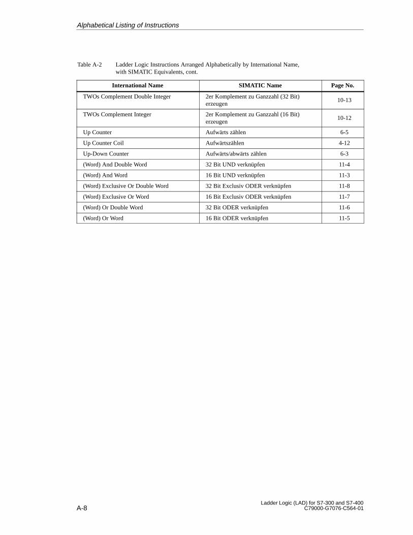
A-8Ladder Logic (LAD) for S7-300 and S7-400
C79000-G7076-C564-01
Table A-2 Ladder Logic Instructions Arranged Alphabetically by International Name,with SIMATIC Equivalents, cont.
International Name Page No.SIMATIC Name
TWOs Complement Double Integer 2er Komplement zu Ganzzahl (32 Bit)erzeugen
10-13
TWOs Complement Integer 2er Komplement zu Ganzzahl (16 Bit)erzeugen
10-12
Up Counter Aufwärts zählen 6-5
Up Counter Coil Aufwärtszählen 4-12
Up-Down Counter Aufwärts/abwärts zählen 6-3
(Word) And Double Word 32 Bit UND verknüpfen 11-4
(Word) And Word 16 Bit UND verknüpfen 11-3
(Word) Exclusive Or Double Word 32 Bit Exclusiv ODER verknüpfen 11-8
(Word) Exclusive Or Word 16 Bit Exclusiv ODER verknüpfen 11-7
(Word) Or Double Word 32 Bit ODER verknüpfen 11-6
(Word) Or Word 16 Bit ODER verknüpfen 11-5
Alphabetical Listing of Instructions
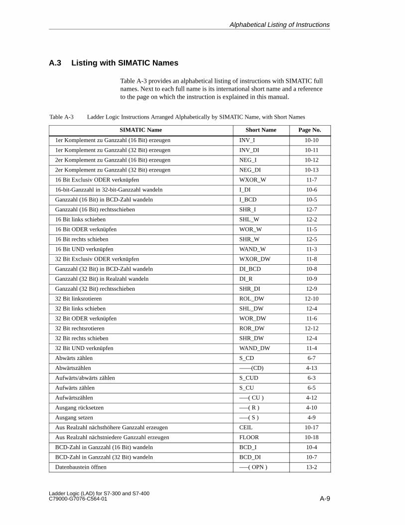
A-9Ladder Logic (LAD) for S7-300 and S7-400C79000-G7076-C564-01
A.3 Listing with SIMATIC Names
Table A-3 provides an alphabetical listing of instructions with SIMATIC fullnames. Next to each full name is its international short name and a referenceto the page on which the instruction is explained in this manual.
Table A-3 Ladder Logic Instructions Arranged Alphabetically by SIMATIC Name, with Short Names
SIMATIC Name Short Name Page No.
1er Komplement zu Ganzzahl (16 Bit) erzeugen INV_I 10-10
1er Komplement zu Ganzzahl (32 Bit) erzeugen INV_DI 10-11
2er Komplement zu Ganzzahl (16 Bit) erzeugen NEG_I 10-12
2er Komplement zu Ganzzahl (32 Bit) erzeugen NEG_DI 10-13
16 Bit Exclusiv ODER verknüpfen WXOR_W 11-7
16-bit-Ganzzahl in 32-bit-Ganzzahl wandeln I_DI 10-6
Ganzzahl (16 Bit) in BCD-Zahl wandeln I_BCD 10-5
Ganzzahl (16 Bit) rechtsschieben SHR_I 12-7
16 Bit links schieben SHL_W 12-2
16 Bit ODER verknüpfen WOR_W 11-5
16 Bit rechts schieben SHR_W 12-5
16 Bit UND verknüpfen WAND_W 11-3
32 Bit Exclusiv ODER verknüpfen WXOR_DW 11-8
Ganzzahl (32 Bit) in BCD-Zahl wandeln DI_BCD 10-8
Ganzzahl (32 Bit) in Realzahl wandeln DI_R 10-9
Ganzzahl (32 Bit) rechtsschieben SHR_DI 12-9
32 Bit linksrotieren ROL_DW 12-10
32 Bit links schieben SHL_DW 12-4
32 Bit ODER verknüpfen WOR_DW 11-6
32 Bit rechtsrotieren ROR_DW 12-12
32 Bit rechts schieben SHR_DW 12-4
32 Bit UND verknüpfen WAND_DW 11-4
Abwärts zählen S_CD 6-7
Abwärtszählen ––––(CD) 4-13
Aufwärts/abwärts zählen S_CUD 6-3
Aufwärts zählen S_CU 6-5
Aufwärtszählen –––( CU ) 4-12
Ausgang rücksetzen –––( R ) 4-10
Ausgang setzen –––( S ) 4-9
Aus Realzahl nächsthöhere Ganzzahl erzeugen CEIL 10-17
Aus Realzahl nächstniedere Ganzzahl erzeugen FLOOR 10-18
BCD-Zahl in Ganzzahl (16 Bit) wandeln BCD_I 10-4
BCD-Zahl in Ganzzahl (32 Bit) wandeln BCD_DI 10-7
Datenbaustein öffnen –––( OPN ) 13-2
Alphabetical Listing of Instructions
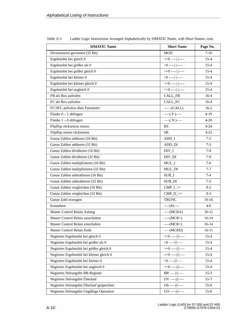
A-10Ladder Logic (LAD) for S7-300 and S7-400
C79000-G7076-C564-01
Table A-3 Ladder Logic Instructions Arranged Alphabetically by SIMATIC Name, with Short Names, cont.
SIMATIC Name Page No.Short Name
Divisionsrest gewinnen (32 Bit) MOD 7-10
Ergebnisbit bei gleich 0 ==0 –––| |––– 15-4
Ergebnisbit bei größer als 0 >0 –––| |––– 15-4
Ergebnisbit bei größer gleich 0 >=0 –––| |––– 15-4
Ergebnisbit bei kleiner 0 <0 –––| |––– 15-4
Ergebnisbit bei kleiner gleich 0 <=0 –––| |––– 15-4
Ergebnisbit bei ungleich 0 <>0 –––| |––– 15-4
FB als Box aufrufen CALL_FB 16-4
FC als Box aufrufen CALL_FC 16-4
FC/SFC aufrufen ohne Parameter ––––(CALL) 16-2
Flanke 0→1 abfragen –––( P )––– 4-19
Flanke 1→0 abfragen –––( N )––– 4-20
Flipflop rücksetzen setzen RS 4-24
Flipflop setzen rücksetzen SR 4-23
Ganze Zahlen addieren (16 Bit) ADD_I 7-2
Ganze Zahlen addieren (32 Bit) ADD_DI 7-3
Ganze Zahlen dividieren (16 Bit) DIV_I 7-8
Ganze Zahlen dividieren (32 Bit) DIV_DI 7-9
Ganze Zahlen multiplizieren (16 Bit) MUL_I 7-6
Ganze Zahlen multiplizieren (32 Bit) MUL_DI 7-7
Ganze Zahlen subtrahieren (16 Bit) SUB_I 7-4
Ganze Zahlen subtrahieren (32 Bit) SUB_DI 7-5
Ganze Zahlen vergleichen (16 Bit) CMP_I_>= 9-2
Ganze Zahlen vergleichen (32 Bit) CMP_D_>= 9-3
Ganze Zahl erzeugen TRUNC 10-16
Konnektor –––(#)––– 4-6
Master Control Relais Anfang –––(MCRA) 16-11
Master Control Relais ausschalten –––(MCR>) 16-14
Master Control Relais einschalten –––(MCR<) 16-14
Master Control Relais Ende –––(MCRD) 16-11
Negiertes Ergebnisbit bei gleich 0 ==0 –––|/|––– 15-4
Negiertes Ergebnisbit bei größer als 0 >0 –––|/|––– 15-4
Negiertes Ergebnisbit bei größer gleich 0 >=0 –––|/|––– 15-4
Negiertes Ergebnisbit bei kleiner gleich 0 <=0 –––|/|––– 15-4
Negiertes Ergebnisbit bei kleiner 0 <0 –––|/|––– 15-4
Negiertes Ergebnisbit bei ungleich 0 <>0 –––|/|––– 15-4
Negiertes Störungsbit BR-Register BR –––|/|––– 15-3
Negiertes Störungsbit Überlauf OV –––|/|––– 15-7
Negiertes Störungsbit Überlauf gespeichert OS –––|/|––– 15-9
Negiertes Störungsbit Ungültige Operation UO –––|/|––– 15-6
Alphabetical Listing of Instructions

A-11Ladder Logic (LAD) for S7-300 and S7-400C79000-G7076-C564-01
Table A-3 Ladder Logic Instructions Arranged Alphabetically by SIMATIC Name, with Short Names, cont.
SIMATIC Name Page No.Short Name
Öffnerkontakt –––|/|––– 4-4
Realzahlen addieren ADD_R 8-3
Realzahlen dividieren DIV_R 8-6
Realzahlen multiplizieren MUL_R 8-5
Realzahlen subtrahieren SUB_R 8-4
Realzahlen vergleichen CMP_R_>= 9-5
Relaisspule, Ausgang –––( ) 4-5
Schließerkontakt –––| |––– 4-3
Signalflanke 0→1 abfragen POS 4-21
Signalflanke 1→0 abfragen NEG 4-22
Springen wenn 0 –––(JMPN) 14-5
Springen wenn 1 –––(JMP) 14-3
Springe zurück –––(RET) 16-8
Störungsbit BR-Register BR –––| |––– 15-3
Störungsbit Überlauf OV –––| |––– 15-7
Störungsbit Überlauf gespeichert OS –––| |––– 15-9
Störungsbit Ungültige Operation UO –––| |––– 15-6
System FB als Box aufrufen CALL_SFB 16-4
System FC als Box aufrufen CALL_SFC 16-4
Verknüpfungsergebnis ins BR-Register laden –––( SAVE ) 4-8
Verknüpfungsergebnis invertieren –––| NOT |––– 4-7
Vorzeichen einer Realzahl wechseln NEG_R 10-14
Wert übertragen MOVE 10-2
Zahl runden ROUND 10-15
Zähleranfangswert setzen –––( SC ) 4-11
Zeit als Ausschaltverzögerung starten (SA) S_OFFDT 5-13
Zeit als Ausschaltverzögerung starten (SA) –––( SF ) 4-18
Zeit als Einschaltverzögerung starten (SE) S_ODT 5-9
Zeit als Einschaltverzögerung starten (SE) –––( SD ) 4-16
Zeit als Impuls starten (SI) S_PULSE 5-5
Zeit als Impuls starten (SI) –––( SP ) 4-14
Zeit als speich. Einschaltverzögerung starten (SS) S_ODTS 5-11
Zeit als speich. Einschaltverzögerung starten (SS) –––( SS ) 4-17
Zeit als verlängerten Impuls starten (SV) S_PEXT 5-7
Zeit als verlängerten Impuls starten (SV) –––( SE ) 4-15
Alphabetical Listing of Instructions
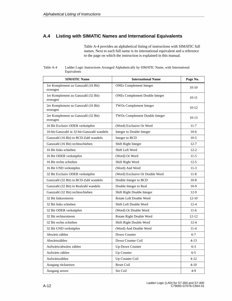
A-12Ladder Logic (LAD) for S7-300 and S7-400
C79000-G7076-C564-01
A.4 Listing with SIMATIC Names and International Equivalents
Table A-4 provides an alphabetical listing of instructions with SIMATIC fullnames. Next to each full name is its international equivalent and a referenceto the page on which the instruction is explained in this manual.
Table A-4 Ladder Logic Instructions Arranged Alphabetically by SIMATIC Name, with InternationalEquivalents
SIMATIC Name International Name Page No.
1er Komplement zu Ganzzahl (16 Bit)erzeugen
ONEs Complement Integer10-10
1er Komplement zu Ganzzahl (32 Bit)erzeugen
ONEs Complement Double Integer10-11
2er Komplement zu Ganzzahl (16 Bit)erzeugen
TWOs Complement Integer10-12
2er Komplement zu Ganzzahl (32 Bit)erzeugen
TWOs Complement Double Integer10-13
16 Bit Exclusiv ODER verknüpfen (Word) Exclusive Or Word 11-7
16-bit-Ganzzahl in 32-bit-Ganzzahl wandeln Integer to Double Integer 10-6
Ganzzahl (16 Bit) in BCD-Zahl wandeln Integer to BCD 10-5
Ganzzahl (16 Bit) rechtsschieben Shift Right Integer 12-7
16 Bit links schieben Shift Left Word 12-2
16 Bit ODER verknüpfen (Word) Or Word 11-5
16 Bit rechts schieben Shift Right Word 12-5
16 Bit UND verknüpfen (Word) And Word 11-3
32 Bit Exclusiv ODER verknüpfen (Word) Exclusive Or Double Word 11-8
Ganzzahl (32 Bit) in BCD-Zahl wandeln Double Integer to BCD 10-8
Ganzzahl (32 Bit) in Realzahl wandeln Double Integer to Real 10-9
Ganzzahl (32 Bit) rechtsschieben Shift Right Double Integer 12-9
32 Bit linksrotieren Rotate Left Double Word 12-10
32 Bit links schieben Shift Left Double Word 12-4
32 Bit ODER verknüpfen (Word) Or Double Word 11-6
32 Bit rechtsrotieren Rotate Right Double Word 12-12
32 Bit rechts schieben Shift Right Double Word 12-4
32 Bit UND verknüpfen (Word) And Double Word 11-4
Abwärts zählen Down Counter 6-7
Abwärtszählen Down Counter Coil 4-13
Aufwärts/abwärts zählen Up-Down Counter 6-3
Aufwärts zählen Up Counter 6-5
Aufwärtszählen Up Counter Coil 4-12
Ausgang rücksetzen Reset Coil 4-10
Ausgang setzen Set Coil 4-9
Alphabetical Listing of Instructions

A-13Ladder Logic (LAD) for S7-300 and S7-400C79000-G7076-C564-01
Table A-4 Ladder Logic Instructions Arranged Alphabetically by SIMATIC Name, with InternationalEquivalents, cont.
SIMATIC Name Page No.International Name
Aus Realzahl nächsthöhere Ganzzahl erzeugenCeiling 10-17
Aus Realzahl nächstniedere Ganzzahlerzeugen
Floor10-18
BCD-Zahl in Ganzzahl (16 Bit) wandeln BCD to Integer 10-4
BCD-Zahl in Ganzzahl (32 Bit) wandeln BCD to Double Integer 10-7
Datenbaustein öffnen Open Data Block: DB or DI 13-2
Divisionsrest gewinnen (32 Bit) Return Fraction Double Integer 7-10
Ergebnisbit bei gleich 0 Result Bit Equal 0 15-4
Ergebnisbit bei größer als 0 Result Bit Greater Than 0 15-4
Ergebnisbit bei größer gleich 0 Result Bit Greater Equal 0 15-4
Ergebnisbit bei kleiner 0 Result Bit Less Than 0 15-4
Ergebnisbit bei kleiner gleich 0 Result Bit Less Equal 0 15-4
Ergebnisbit bei ungleich 0 Result Bit Not Equal 0 15-4
FB als Box aufrufen Call FB from Box 16-4
FC als Box aufrufen Call FC from Box 16-4
FC/SFC aufrufen ohne Parameter Call FC SFC from Coil (without parameters) 16-2
Flanke 0→1 abfragen Positive RLO Edge Detection 4-19
Flanke 1→0 abfragen Negative RLO Edge Detection 4-20
Flipflop rücksetzen setzen Reset-Set Flipflop 4-24
Flipflop setzen rücksetzen Set-Reset Flipflop 4-23
Ganze Zahlen addieren (16 Bit) Add Integer 7-2
Ganze Zahlen addieren (32 Bit) Add Double Integer 7-3
Ganze Zahlen dividieren (16 Bit) Divide Integer 7-8
Ganze Zahlen dividieren (32 Bit) Divide Double Integer 7-9
Ganze Zahlen multiplizieren (16 Bit) Multiply Integer 7-6
Ganze Zahlen multiplizieren (32 Bit) Multiply Double Integer 7-7
Ganze Zahlen subtrahieren (16 Bit) Subtract Integer 7-4
Ganze Zahlen subtrahieren (32 Bit) Subtract Double Integer 7-5
Ganze Zahlen vergleichen (16 Bit) Compare Integer (>, <, ==, <>, <=, >=) 9-2
Ganze Zahlen vergleichen (32 Bit) Compare Double Integer(>, <, ==, <>, <=, >=)
9-3
Ganze Zahl erzeugen Truncate Double Integer Part 10-16
Konnektor Midline Output 4-6
Master Control Relais Anfang Master Control Relay Activate 16-11
Master Control Relais ausschalten Master Control Relay Off 16-14
Master Control Relais einschalten Master Control Relay On 16-14
Master Control Relais Ende Master Control Relay Deactivate 16-11
Alphabetical Listing of Instructions
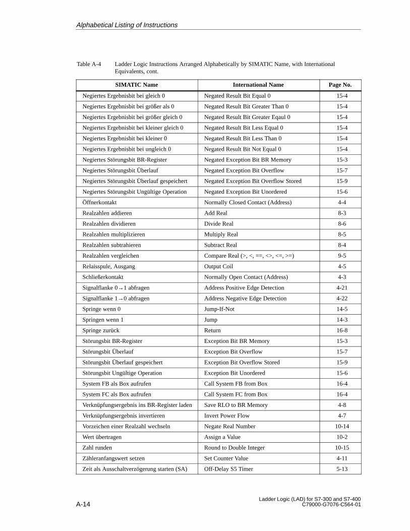
A-14Ladder Logic (LAD) for S7-300 and S7-400
C79000-G7076-C564-01
Table A-4 Ladder Logic Instructions Arranged Alphabetically by SIMATIC Name, with InternationalEquivalents, cont.
SIMATIC Name Page No.International Name
Negiertes Ergebnisbit bei gleich 0 Negated Result Bit Equal 0 15-4
Negiertes Ergebnisbit bei größer als 0 Negated Result Bit Greater Than 0 15-4
Negiertes Ergebnisbit bei größer gleich 0 Negated Result Bit Greater Eqaul 0 15-4
Negiertes Ergebnisbit bei kleiner gleich 0 Negated Result Bit Less Equal 0 15-4
Negiertes Ergebnisbit bei kleiner 0 Negated Result Bit Less Than 0 15-4
Negiertes Ergebnisbit bei ungleich 0 Negated Result Bit Not Equal 0 15-4
Negiertes Störungsbit BR-Register Negated Exception Bit BR Memory 15-3
Negiertes Störungsbit Überlauf Negated Exception Bit Overflow 15-7
Negiertes Störungsbit Überlauf gespeichert Negated Exception Bit Overflow Stored 15-9
Negiertes Störungsbit Ungültige Operation Negated Exception Bit Unordered 15-6
Öffnerkontakt Normally Closed Contact (Address) 4-4
Realzahlen addieren Add Real 8-3
Realzahlen dividieren Divide Real 8-6
Realzahlen multiplizieren Multiply Real 8-5
Realzahlen subtrahieren Subtract Real 8-4
Realzahlen vergleichen Compare Real (>, <, ==, <>, <=, >=) 9-5
Relaisspule, Ausgang Output Coil 4-5
Schließerkontakt Normally Open Contact (Address) 4-3
Signalflanke 0→1 abfragen Address Positive Edge Detection 4-21
Signalflanke 1→0 abfragen Address Negative Edge Detection 4-22
Springe wenn 0 Jump-If-Not 14-5
Springen wenn 1 Jump 14-3
Springe zurück Return 16-8
Störungsbit BR-Register Exception Bit BR Memory 15-3
Störungsbit Überlauf Exception Bit Overflow 15-7
Störungsbit Überlauf gespeichert Exception Bit Overflow Stored 15-9
Störungsbit Ungültige Operation Exception Bit Unordered 15-6
System FB als Box aufrufen Call System FB from Box 16-4
System FC als Box aufrufen Call System FC from Box 16-4
Verknüpfungsergebnis ins BR-Register laden Save RLO to BR Memory 4-8
Verknüpfungsergebnis invertieren Invert Power Flow 4-7
Vorzeichen einer Realzahl wechseln Negate Real Number 10-14
Wert übertragen Assign a Value 10-2
Zahl runden Round to Double Integer 10-15
Zähleranfangswert setzen Set Counter Value 4-11
Zeit als Ausschaltverzögerung starten (SA) Off-Delay S5 Timer 5-13
Alphabetical Listing of Instructions
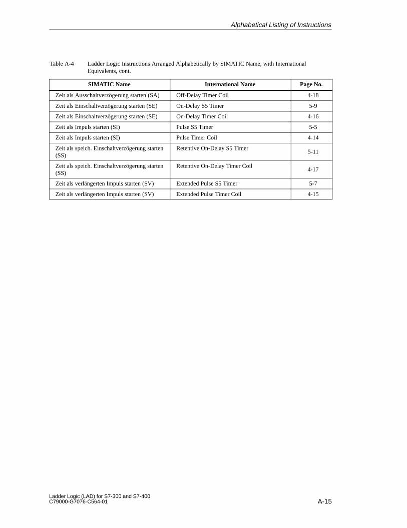
A-15Ladder Logic (LAD) for S7-300 and S7-400C79000-G7076-C564-01
Table A-4 Ladder Logic Instructions Arranged Alphabetically by SIMATIC Name, with InternationalEquivalents, cont.
SIMATIC Name Page No.International Name
Zeit als Ausschaltverzögerung starten (SA) Off-Delay Timer Coil 4-18
Zeit als Einschaltverzögerung starten (SE) On-Delay S5 Timer 5-9
Zeit als Einschaltverzögerung starten (SE) On-Delay Timer Coil 4-16
Zeit als Impuls starten (SI) Pulse S5 Timer 5-5
Zeit als Impuls starten (SI) Pulse Timer Coil 4-14
Zeit als speich. Einschaltverzögerung starten(SS)
Retentive On-Delay S5 Timer5-11
Zeit als speich. Einschaltverzögerung starten(SS)
Retentive On-Delay Timer Coil4-17
Zeit als verlängerten Impuls starten (SV) Extended Pulse S5 Timer 5-7
Zeit als verlängerten Impuls starten (SV) Extended Pulse Timer Coil 4-15
Alphabetical Listing of Instructions
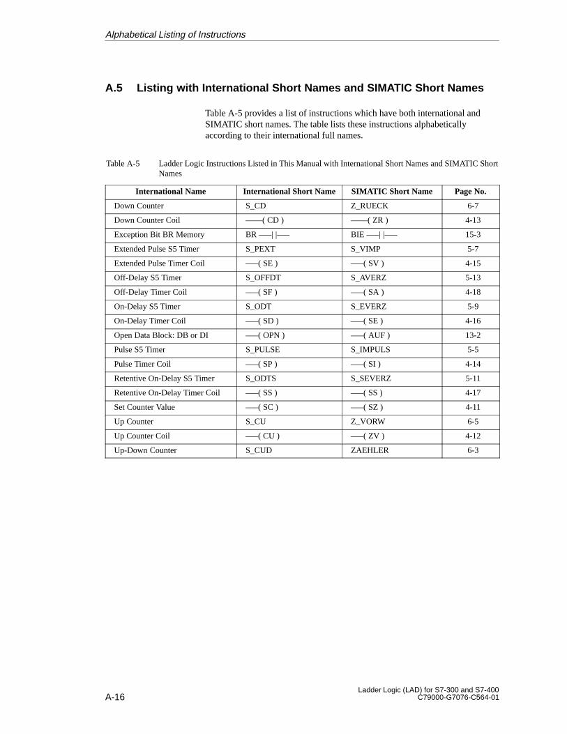
A-16Ladder Logic (LAD) for S7-300 and S7-400
C79000-G7076-C564-01
A.5 Listing with International Short Names and SIMATIC Short Names
Table A-5 provides a list of instructions which have both international andSIMATIC short names. The table lists these instructions alphabeticallyaccording to their international full names.
Table A-5 Ladder Logic Instructions Listed in This Manual with International Short Names and SIMATIC ShortNames
International Name International Short Name SIMATIC Short Name Page No.
Down Counter S_CD Z_RUECK 6-7
Down Counter Coil ––––( CD ) ––––( ZR ) 4-13
Exception Bit BR Memory BR –––| |––– BIE –––| |––– 15-3
Extended Pulse S5 Timer S_PEXT S_VIMP 5-7
Extended Pulse Timer Coil –––( SE ) –––( SV ) 4-15
Off-Delay S5 Timer S_OFFDT S_AVERZ 5-13
Off-Delay Timer Coil –––( SF ) –––( SA ) 4-18
On-Delay S5 Timer S_ODT S_EVERZ 5-9
On-Delay Timer Coil –––( SD ) –––( SE ) 4-16
Open Data Block: DB or DI –––( OPN ) –––( AUF ) 13-2
Pulse S5 Timer S_PULSE S_IMPULS 5-5
Pulse Timer Coil –––( SP ) –––( SI ) 4-14
Retentive On-Delay S5 Timer S_ODTS S_SEVERZ 5-11
Retentive On-Delay Timer Coil –––( SS ) –––( SS ) 4-17
Set Counter Value –––( SC ) –––( SZ ) 4-11
Up Counter S_CU Z_VORW 6-5
Up Counter Coil –––( CU ) –––( ZV ) 4-12
Up-Down Counter S_CUD ZAEHLER 6-3
Alphabetical Listing of Instructions
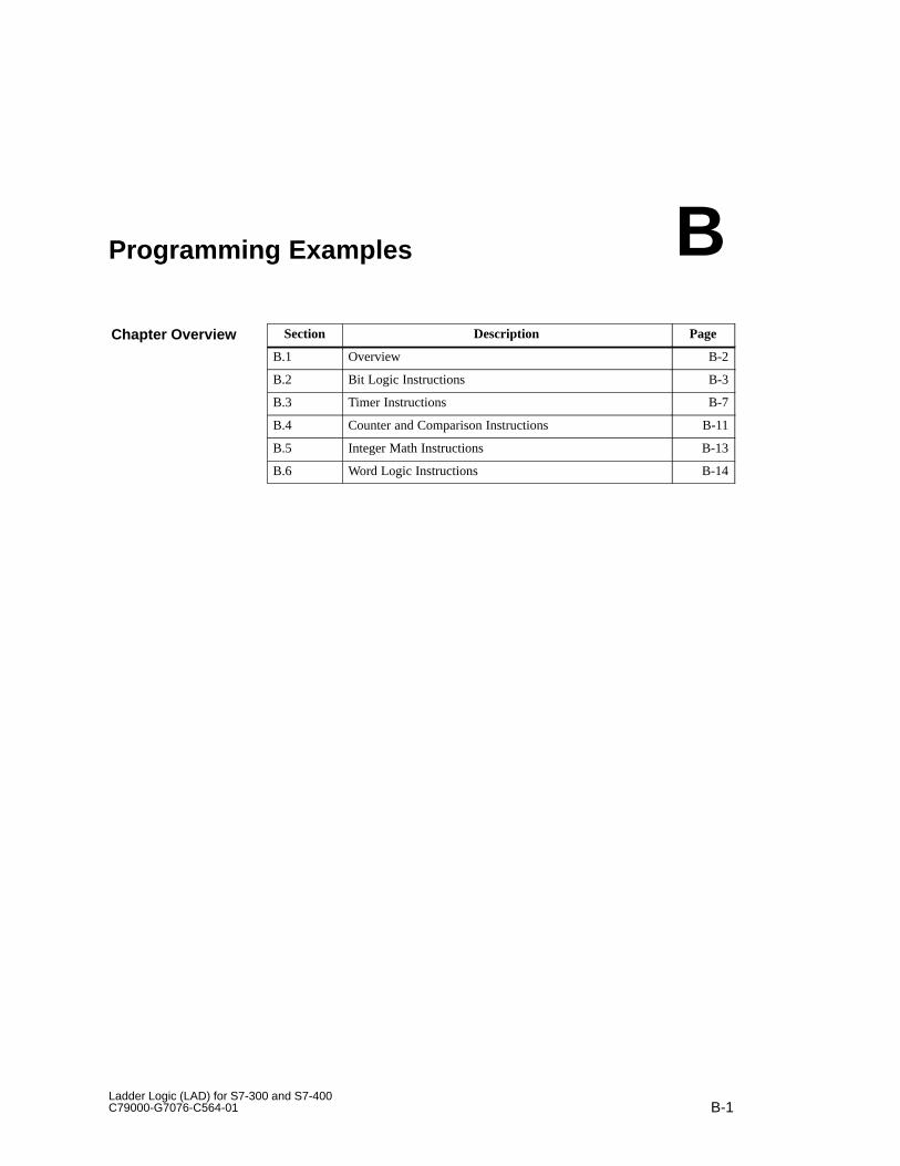
B-1Ladder Logic (LAD) for S7-300 and S7-400C79000-G7076-C564-01
Programming Examples
Section Description Page
B.1 Overview B-2
B.2 Bit Logic Instructions B-3
B.3 Timer Instructions B-7
B.4 Counter and Comparison Instructions B-11
B.5 Integer Math Instructions B-13
B.6 Word Logic Instructions B-14
Chapter Overview
B
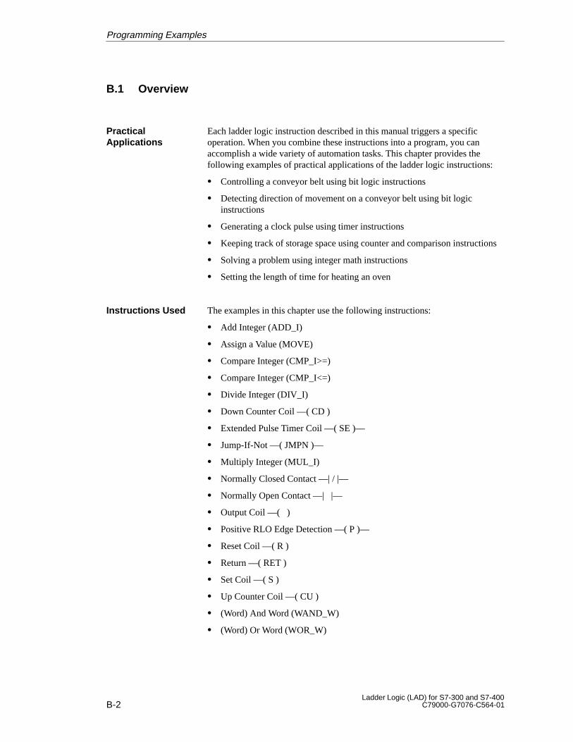
B-2Ladder Logic (LAD) for S7-300 and S7-400
C79000-G7076-C564-01
B.1 Overview
Each ladder logic instruction described in this manual triggers a specificoperation. When you combine these instructions into a program, you canaccomplish a wide variety of automation tasks. This chapter provides thefollowing examples of practical applications of the ladder logic instructions:
� Controlling a conveyor belt using bit logic instructions
� Detecting direction of movement on a conveyor belt using bit logicinstructions
� Generating a clock pulse using timer instructions
� Keeping track of storage space using counter and comparison instructions
� Solving a problem using integer math instructions
� Setting the length of time for heating an oven
The examples in this chapter use the following instructions:
� Add Integer (ADD_I)
� Assign a Value (MOVE)
� Compare Integer (CMP_I>=)
� Compare Integer (CMP_I<=)
� Divide Integer (DIV_I)
� Down Counter Coil ––( CD )
� Extended Pulse Timer Coil ––( SE )––
� Jump-If-Not ––( JMPN )––
� Multiply Integer (MUL_I)
� Normally Closed Contact ––| / |––
� Normally Open Contact ––| |––
� Output Coil ––( )
� Positive RLO Edge Detection ––( P )––
� Reset Coil ––( R )
� Return ––( RET )
� Set Coil ––( S )
� Up Counter Coil ––( CU )
� (Word) And Word (WAND_W)
� (Word) Or Word (WOR_W)
PracticalApplications
Instructions Used
Programming Examples
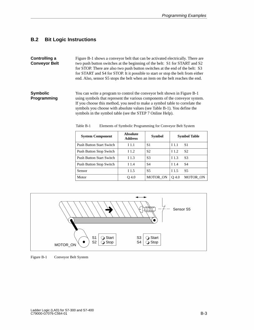
B-3Ladder Logic (LAD) for S7-300 and S7-400C79000-G7076-C564-01
B.2 Bit Logic Instructions
Figure B-1 shows a conveyor belt that can be activated electrically. There aretwo push button switches at the beginning of the belt: S1 for START and S2for STOP. There are also two push button switches at the end of the belt: S3for START and S4 for STOP. It it possible to start or stop the belt from eitherend. Also, sensor S5 stops the belt when an item on the belt reaches the end.
You can write a program to control the conveyor belt shown in Figure B-1using symbols that represent the various components of the conveyor system.If you choose this method, you need to make a symbol table to correlate thesymbols you choose with absolute values (see Table B-1). You define thesymbols in the symbol table (see the STEP 7 Online Help).
Table B-1 Elements of Symbolic Programming for Conveyor Belt System
System ComponentAbsoluteAddress
Symbol Symbol Table
Push Button Start Switch I 1.1 S1 I 1.1 S1
Push Button Stop Switch I 1.2 S2 I 1.2 S2
Push Button Start Switch I 1.3 S3 I 1.3 S3
Push Button Stop Switch I 1.4 S4 I 1.4 S4
Sensor I 1.5 S5 I 1.5 S5
Motor Q 4.0 MOTOR_ON Q 4.0 MOTOR_ON
MOTOR_ON
S1S2
� Start� Stop
S3S4
� Start� Stop
Sensor S5
Figure B-1 Conveyor Belt System
Controlling aConveyor Belt
SymbolicProgramming
Programming Examples
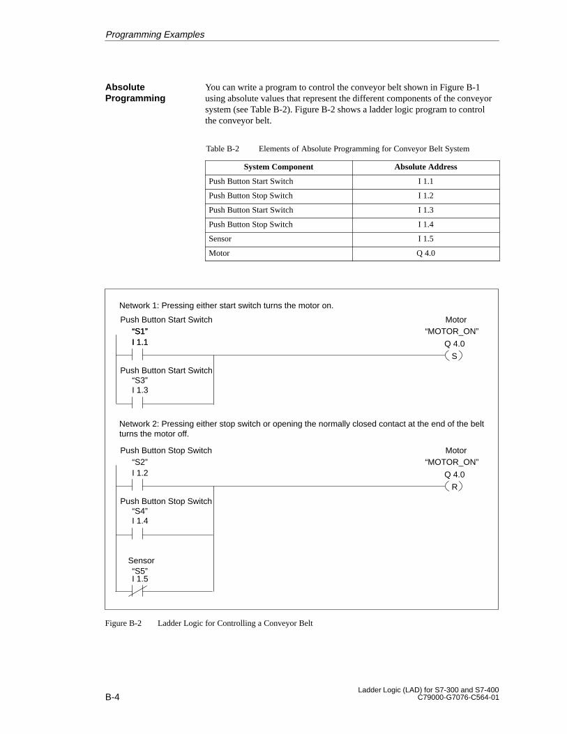
B-4Ladder Logic (LAD) for S7-300 and S7-400
C79000-G7076-C564-01
You can write a program to control the conveyor belt shown in Figure B-1using absolute values that represent the different components of the conveyorsystem (see Table B-2). Figure B-2 shows a ladder logic program to controlthe conveyor belt.
Table B-2 Elements of Absolute Programming for Conveyor Belt System
System Component Absolute Address
Push Button Start Switch I 1.1
Push Button Stop Switch I 1.2
Push Button Start Switch I 1.3
Push Button Stop Switch I 1.4
Sensor I 1.5
Motor Q 4.0
I 1.1 Q 4.0
Push Button Start Switch“S1”“S1”
S
Motor“MOTOR_ON”
Push Button Start Switch
I 1.1
“S3”I 1.3
Network 1: Pressing either start switch turns the motor on.
Network 2: Pressing either stop switch or opening the normally closed contact at the end of the beltturns the motor off.
Q 4.0
Push Button Stop Switch“S2”
R
Motor“MOTOR_ON”
Push Button Stop Switch
I 1.2
“S4”I 1.4
Sensor“S5”I 1.5
Figure B-2 Ladder Logic for Controlling a Conveyor Belt
AbsoluteProgramming
Programming Examples
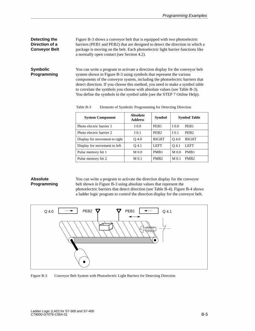
B-5Ladder Logic (LAD) for S7-300 and S7-400C79000-G7076-C564-01
Figure B-3 shows a conveyor belt that is equipped with two photoelectricbarriers (PEB1 and PEB2) that are designed to detect the direction in which apackage is moving on the belt. Each photoelectric light barrier functions likea normally open contact (see Section 4.2).
You can write a program to activate a direction display for the conveyor beltsystem shown in Figure B-3 using symbols that represent the variouscomponents of the conveyor system, including the photoelectric barriers thatdetect direction. If you choose this method, you need to make a symbol tableto correlate the symbols you choose with absolute values (see Table B-3).You define the symbols in the symbol table (see the STEP 7 Online Help).
Table B-3 Elements of Symbolic Programming for Detecting Direction
System ComponentAbsoluteAddress
Symbol Symbol Table
Photo electric barrier 1 I 0.0 PEB1 I 0.0 PEB1
Photo electric barrier 2 I 0.1 PEB2 I 0.1 PEB2
Display for movement to right Q 4.0 RIGHT Q 4.0 RIGHT
Display for movement to left Q 4.1 LEFT Q 4.1 LEFT
Pulse memory bit 1 M 0.0 PMB1 M 0.0 PMB1
Pulse memory bit 2 M 0.1 PMB2 M 0.1 PMB2
You can write a program to activate the direction display for the conveyorbelt shown in Figure B-3 using absolute values that represent thephotoelectric barriers that detect direction (see Table B-4). Figure B-4 showsa ladder logic program to control the direction display for the conveyor belt.
PEB1PEB2 Q 4.1Q 4.0
Figure B-3 Conveyor Belt System with Photoelectric Light Barriers for Detecting Direction
Detecting theDirection of aConveyor Belt
SymbolicProgramming
AbsoluteProgramming
Programming Examples
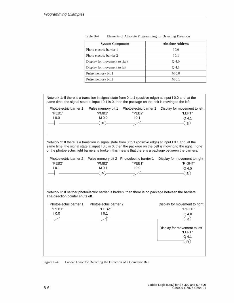
B-6Ladder Logic (LAD) for S7-300 and S7-400
C79000-G7076-C564-01
Table B-4 Elements of Absolute Programming for Detecting Direction
System Component Absolute Address
Photo electric barrier 1 I 0.0
Photo electric barrier 2 I 0.1
Display for movement to right Q 4.0
Display for movement to left Q 4.1
Pulse memory bit 1 M 0.0
Pulse memory bit 2 M 0.1
Q 4.1
Photoelectric barrier 1“PEB1”
S
Display for movement to left“LEFT”
I 0.0
Network 1: If there is a transition in signal state from 0 to 1 (positive edge) at input I 0.0 and, at thesame time, the signal state at input I 0.1 is 0, then the package on the belt is moving to the left.
Pulse memory bit 1 Photoelectric barrier 2
P
“PMB1” “PEB2”I 0.1M 0.0
Network 2: If there is a transition in signal state from 0 to 1 (positive edge) at input I 0.1 and, at thesame time, the signal state at input I 0.0 is 0, then the package on the belt is moving to the right. If oneof the photoelectric light barriers is broken, this means that there is a package between the barriers.
Q 4.0
Photoelectric barrier 2“PEB2”
S
Display for movement to right“RIGHT”
I 0.1
Pulse memory bit 2 Photoelectric barrier 1
P
“PMB2” “PEB1”I 0.0M 0.1
Network 3: If neither photoelectric barrier is broken, then there is no package between the barriers.The direction pointer shuts off.
Q 4.0
Photoelectric barrier 1“PEB1”
R
Display for movement to right“RIGHT”
I 0.0
Photoelectric barrier 2“PEB2”I 0.1
Display for movement to left
Q 4.1
R
“LEFT”
Figure B-4 Ladder Logic for Detecting the Direction of a Conveyor Belt
Programming Examples
B-7Ladder Logic (LAD) for S7-300 and S7-400C79000-G7076-C564-01
B.3 Timer Instructions
You can use a clock pulse generator or flasher relay when you need toproduce a signal that repeats periodically. A clock pulse generator is commonin a signalling system that controls the flashing of indicator lamps.
When you use the S7-300, you can implement the clock pulse generatorfunction by using time-driven processing in special organization blocks. Theexample shown in the following ladder logic program, however, illustratesthe use of timer functions to generate a clock pulse.
The sample program in Figure B-5 shows how to implement a freewheelingclock pulse generator by using a timer (pulse duty factor 1:1). The frequencyis divided into the values listed in Table B-5.
Clock PulseGenerator
Programming Examples
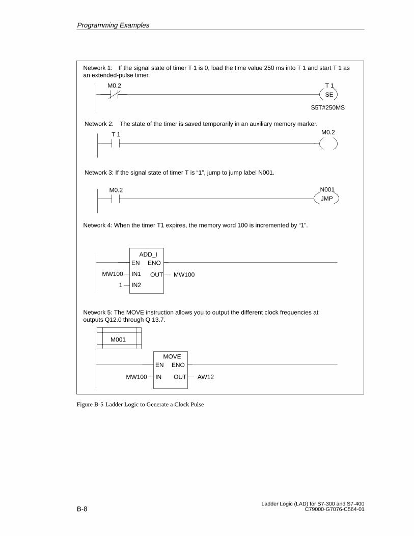
B-8Ladder Logic (LAD) for S7-300 and S7-400
C79000-G7076-C564-01
MW100
M0.2 T 1
SE
S5T#250MS
M0.2
Network 1: If the signal state of timer T 1 is 0, load the time value 250 ms into T 1 and start T 1 asan extended-pulse timer.
Network 4: When the timer T1 expires, the memory word 100 is incremented by “1”.
ADD_I
IN1
ENOEN
IN2
OUTMW100
1
MW100
Network 5: The MOVE instruction allows you to output the different clock frequencies atoutputs Q12.0 through Q 13.7.
MOVE
IN
ENOEN
OUT AW12
M001
T 1
Network 2: The state of the timer is saved temporarily in an auxiliary memory marker.
N001
JMP
Network 3: If the signal state of timer T is “1”, jump to jump label N001.
M0.2
Figure B-5 Ladder Logic to Generate a Clock Pulse
Programming Examples
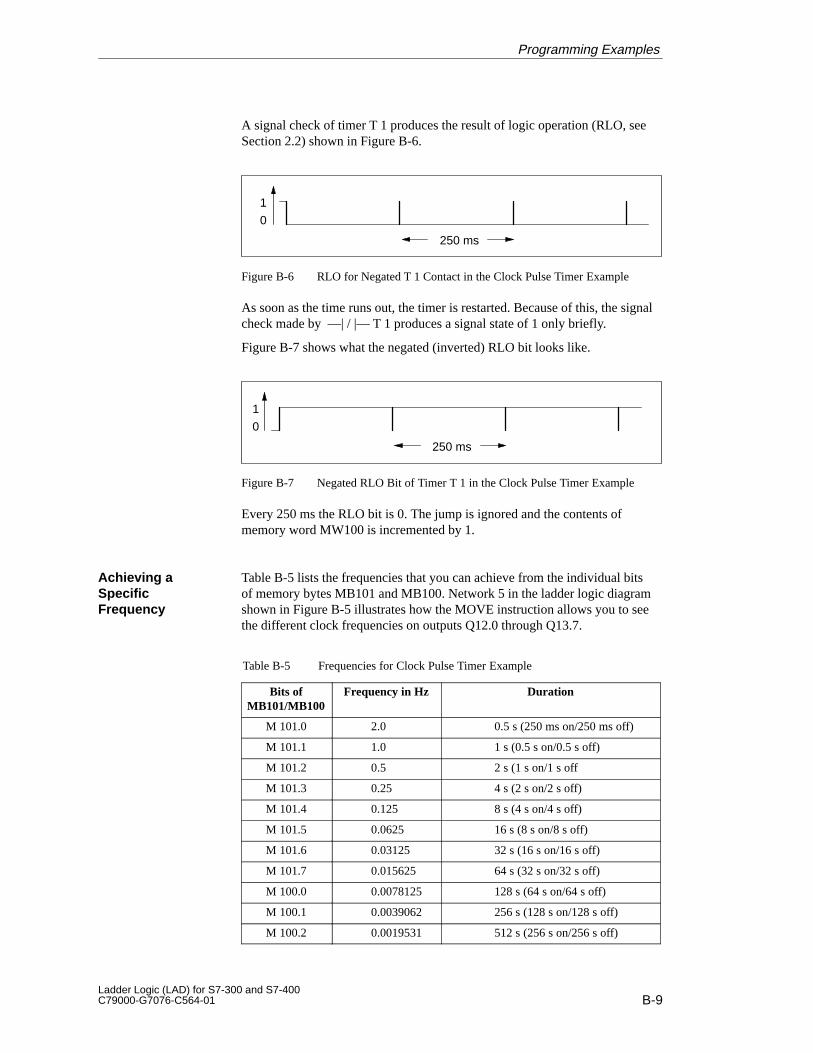
B-9Ladder Logic (LAD) for S7-300 and S7-400C79000-G7076-C564-01
A signal check of timer T 1 produces the result of logic operation (RLO, seeSection 2.2) shown in Figure B-6.
0
1
250 ms
Figure B-6 RLO for Negated T 1 Contact in the Clock Pulse Timer Example
As soon as the time runs out, the timer is restarted. Because of this, the signalcheck made by ––| / |–– T 1 produces a signal state of 1 only briefly.
Figure B-7 shows what the negated (inverted) RLO bit looks like.
0
1
250 ms
Figure B-7 Negated RLO Bit of Timer T 1 in the Clock Pulse Timer Example
Every 250 ms the RLO bit is 0. The jump is ignored and the contents ofmemory word MW100 is incremented by 1.
Table B-5 lists the frequencies that you can achieve from the individual bitsof memory bytes MB101 and MB100. Network 5 in the ladder logic diagramshown in Figure B-5 illustrates how the MOVE instruction allows you to seethe different clock frequencies on outputs Q12.0 through Q13.7.
Table B-5 Frequencies for Clock Pulse Timer Example
Bits ofMB101/MB100
Frequency in Hz Duration
M 101.0 2.0 0.5 s (250 ms on/250 ms off)
M 101.1 1.0 1 s (0.5 s on/0.5 s off)
M 101.2 0.5 2 s (1 s on/1 s off
M 101.3 0.25 4 s (2 s on/2 s off)
M 101.4 0.125 8 s (4 s on/4 s off)
M 101.5 0.0625 16 s (8 s on/8 s off)
M 101.6 0.03125 32 s (16 s on/16 s off)
M 101.7 0.015625 64 s (32 s on/32 s off)
M 100.0 0.0078125 128 s (64 s on/64 s off)
M 100.1 0.0039062 256 s (128 s on/128 s off)
M 100.2 0.0019531 512 s (256 s on/256 s off)
Achieving aSpecificFrequency
Programming Examples
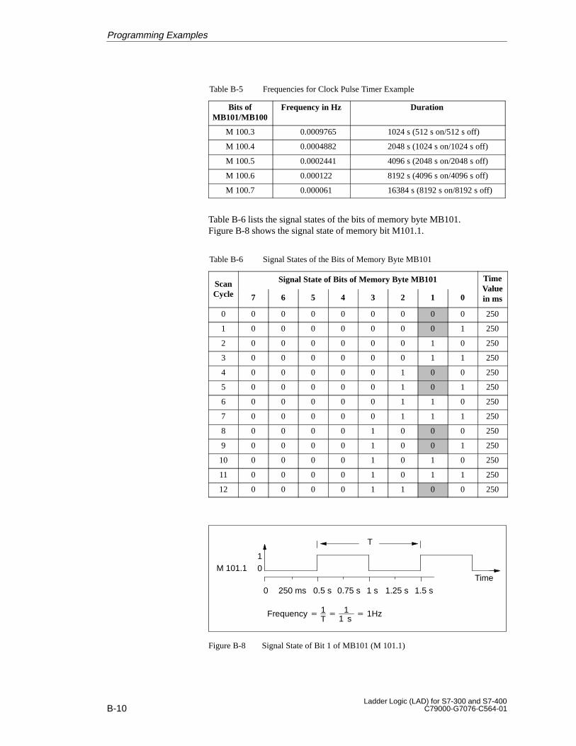
B-10Ladder Logic (LAD) for S7-300 and S7-400
C79000-G7076-C564-01
Table B-5 Frequencies for Clock Pulse Timer Example
Bits ofMB101/MB100
DurationFrequency in Hz
M 100.3 0.0009765 1024 s (512 s on/512 s off)
M 100.4 0.0004882 2048 s (1024 s on/1024 s off)
M 100.5 0.0002441 4096 s (2048 s on/2048 s off)
M 100.6 0.000122 8192 s (4096 s on/4096 s off)
M 100.7 0.000061 16384 s (8192 s on/8192 s off)
Table B-6 lists the signal states of the bits of memory byte MB101.Figure B-8 shows the signal state of memory bit M101.1.
Table B-6 Signal States of the Bits of Memory Byte MB101
Scan Signal State of Bits of Memory Byte MB101 TimeValue
Cycle 7 6 5 4 3 2 1 0Valuein ms
0 0 0 0 0 0 0 0 0 250
1 0 0 0 0 0 0 0 1 250
2 0 0 0 0 0 0 1 0 250
3 0 0 0 0 0 0 1 1 250
4 0 0 0 0 0 1 0 0 250
5 0 0 0 0 0 1 0 1 250
6 0 0 0 0 0 1 1 0 250
7 0 0 0 0 0 1 1 1 250
8 0 0 0 0 1 0 0 0 250
9 0 0 0 0 1 0 0 1 250
10 0 0 0 0 1 0 1 0 250
11 0 0 0 0 1 0 1 1 250
12 0 0 0 0 1 1 0 0 250
M 101.1
250 ms 0.5 s 0.75 s 1 s 1.25 s 1.5 s
T
Time01
Frequency� 1T�
11 s
� 1Hz
0
Figure B-8 Signal State of Bit 1 of MB101 (M 101.1)
Programming Examples
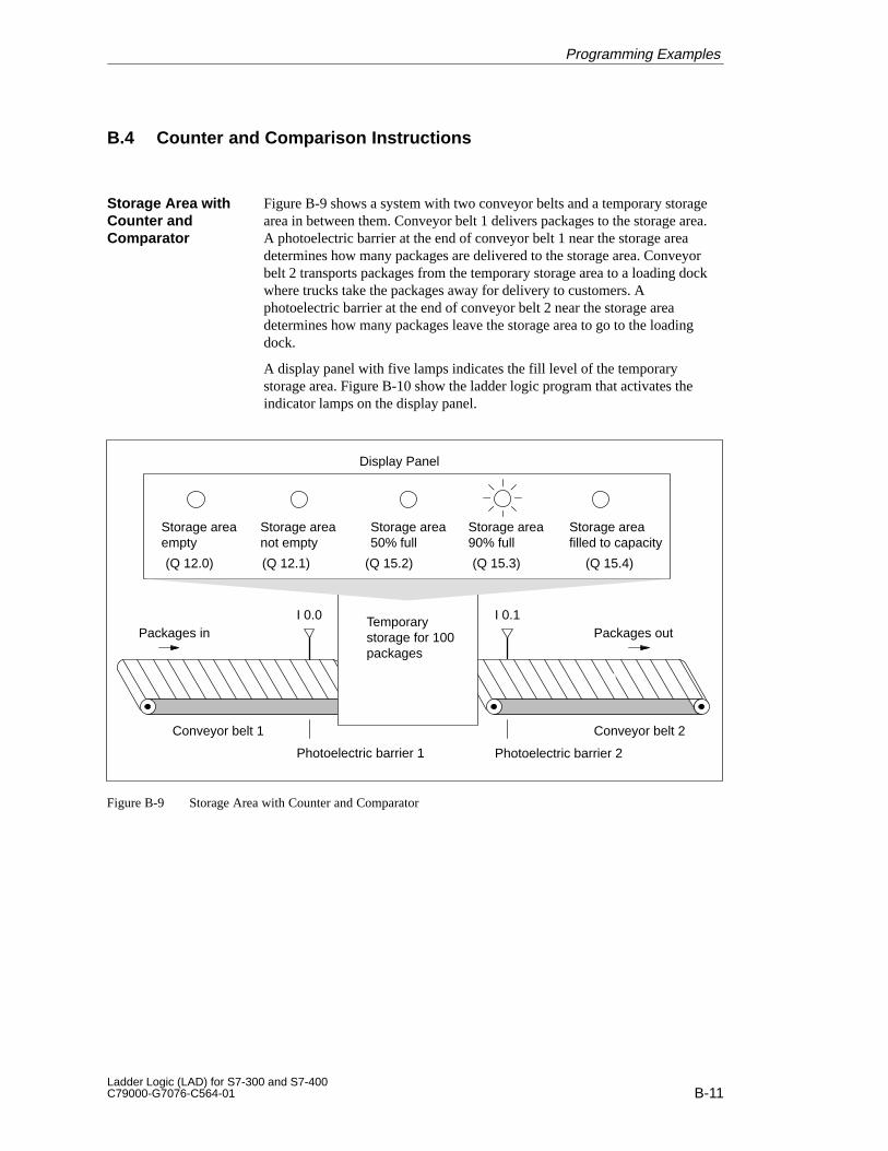
B-11Ladder Logic (LAD) for S7-300 and S7-400C79000-G7076-C564-01
B.4 Counter and Comparison Instructions
Figure B-9 shows a system with two conveyor belts and a temporary storagearea in between them. Conveyor belt 1 delivers packages to the storage area.A photoelectric barrier at the end of conveyor belt 1 near the storage areadetermines how many packages are delivered to the storage area. Conveyorbelt 2 transports packages from the temporary storage area to a loading dockwhere trucks take the packages away for delivery to customers. Aphotoelectric barrier at the end of conveyor belt 2 near the storage areadetermines how many packages leave the storage area to go to the loadingdock.
A display panel with five lamps indicates the fill level of the temporarystorage area. Figure B-10 show the ladder logic program that activates theindicator lamps on the display panel.
Storage areaempty
Display Panel
Storage areafilled to capacity
Storage area90% full
Storage area50% full
Storage areanot empty
Packages in Packages outI 0.0 I 0.1
Conveyor belt 2Conveyor belt 1
Photoelectric barrier 1 Photoelectric barrier 2
Temporarystorage for 100packages
(Q 12.0) (Q 12.1) (Q 15.2) (Q 15.3) (Q 15.4)
Figure B-9 Storage Area with Counter and Comparator
Storage Area withCounter andComparator
Programming Examples
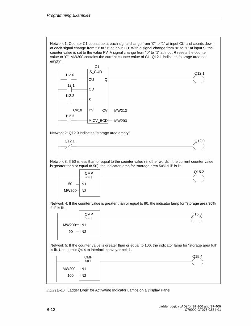
B-12Ladder Logic (LAD) for S7-300 and S7-400
C79000-G7076-C564-01
MW200
I12.0 Q12.1
Network 1: Counter C1 counts up at each signal change from “0” to “1” at input CU and counts downat each signal change from “0” to “1” at input CD. With a signal change from “0” to ”1” at input S, thecounter value is set to the value PV. A signal change from “0” to “1” at input R resets the countervalue to “0”. MW200 contains the current counter value of C1. Q12.1 indicates “storage area notempty”.
Q12.0
Network 2: Q12.0 indicates ”storage area empty”.
Q12.1
Network 3: If 50 is less than or equal to the counter value (in other words if the current counter valueis greater than or equal to 50), the indicator lamp for “storage area 50% full” is lit.
CMP
IN150
Q15.2
IN2
Network 4: If the counter value is greater than or equal to 90, the indicator lamp for “storage area 90%full” is lit.
CMP
IN1
>= I
90
MW200
Q15.3
IN2
<= I
Network 5: If the counter value is greater than or equal to 100, the indicator lamp for “storage area full”is lit. Use output Q4.4 to interlock conveyor belt 1.
CMP
IN1
>= I
100
MW200
Q15.4
IN2
S_CUD
CD
QCU
S
PV CV
R CV_BCDI12.3
I12.2
I12.1
C#10
C1
MW210
MW200
Figure B-10 Ladder Logic for Activating Indicator Lamps on a Display Panel
Programming Examples
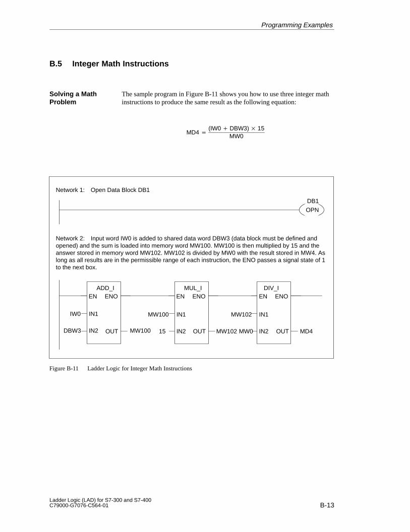
B-13Ladder Logic (LAD) for S7-300 and S7-400C79000-G7076-C564-01
B.5 Integer Math Instructions
The sample program in Figure B-11 shows you how to use three integer mathinstructions to produce the same result as the following equation:
MD4�(IW0�DBW3)� 15
MW0
DB1
OPN
Network 1: Open Data Block DB1
Network 2: Input word IW0 is added to shared data word DBW3 (data block must be defined andopened) and the sum is loaded into memory word MW100. MW100 is then multiplied by 15 and theanswer stored in memory word MW102. MW102 is divided by MW0 with the result stored in MW4. Aslong as all results are in the permissible range of each instruction, the ENO passes a signal state of 1to the next box.
ADD_I
IN1
ENOEN
IN2 OUTDBW3
IW0
MW100
MUL_I
IN1
ENOEN
IN2 OUT
MW100
15 MW102
DIV_I
IN1
ENOEN
IN2 OUT
MW102
MW0 MD4
Figure B-11 Ladder Logic for Integer Math Instructions
Solving a MathProblem
Programming Examples
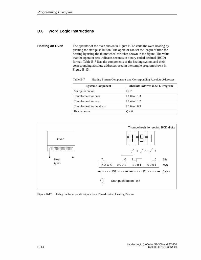
B-14Ladder Logic (LAD) for S7-300 and S7-400
C79000-G7076-C564-01
B.6 Word Logic Instructions
The operator of the oven shown in Figure B-12 starts the oven heating bypushing the start push button. The operator can set the length of time forheating by using the thumbwheel switches shown in the figure. The valuethat the operator sets indicates seconds in binary coded decimal (BCD)format. Table B-7 lists the components of the heating system and theircorresponding absolute addresses used in the sample program shown inFigure B-13.
Table B-7 Heating System Components and Corresponding Absolute Addresses
System Component Absolute Address in STL Program
Start push button I 0.7
Thumbwheel for ones I 1.0 to I 1.3
Thumbwheel for tens I 1.4 to I 1.7
Thumbwheel for hundreds I 0.0 to I 0.3
Heating starts Q 4.0
7....
OvenÎÎÎ
ÎÎÎÎÎÎ
ÎÎÎÎÎÎ
1 0 0 1 0 0 0 1X X X X 0 0 0 1
HeatQ 4.0
Thumbwheels for setting BCD digits
IW0
4 4 4
Start push button I 0.7
IB1IB0 Bytes
Bits7......0 ...0
Figure B-12 Using the Inputs and Outputs for a Time-Limited Heating Process
Heating an Oven
Programming Examples
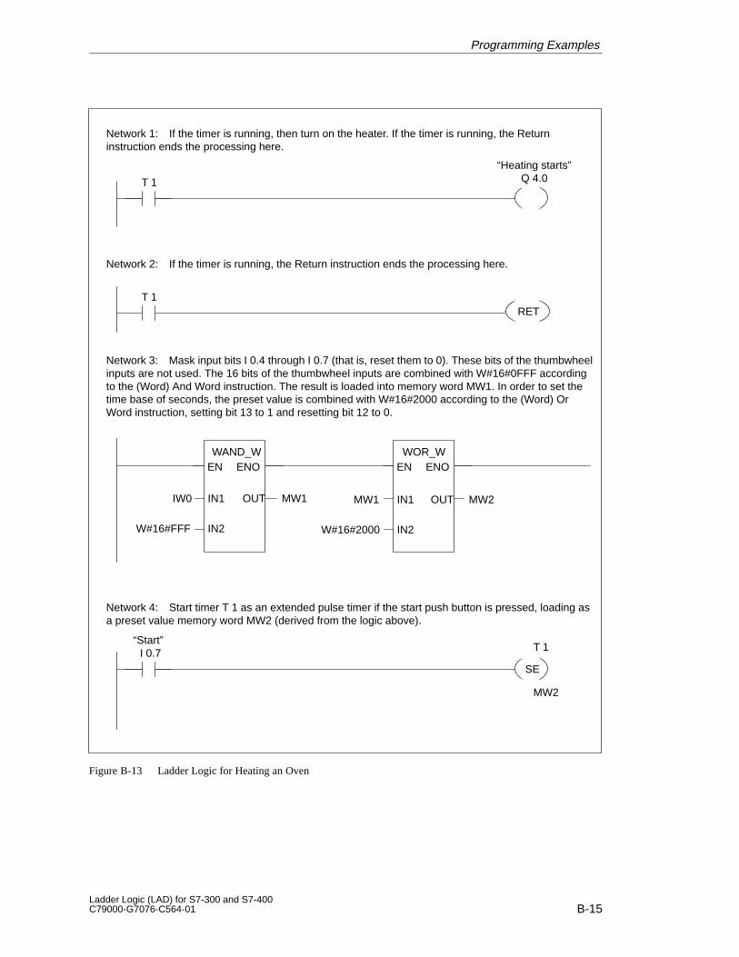
B-15Ladder Logic (LAD) for S7-300 and S7-400C79000-G7076-C564-01
T 1
“Heating starts”Q 4.0
RET
Network 1: If the timer is running, then turn on the heater. If the timer is running, the Returninstruction ends the processing here.
Network 3: Mask input bits I 0.4 through I 0.7 (that is, reset them to 0). These bits of the thumbwheelinputs are not used. The 16 bits of the thumbwheel inputs are combined with W#16#0FFF accordingto the (Word) And Word instruction. The result is loaded into memory word MW1. In order to set thetime base of seconds, the preset value is combined with W#16#2000 according to the (Word) OrWord instruction, setting bit 13 to 1 and resetting bit 12 to 0.
Network 4: Start timer T 1 as an extended pulse timer if the start push button is pressed, loading asa preset value memory word MW2 (derived from the logic above).
WAND_W
IN1
ENOEN
IN2
OUT
W#16#FFF
IW0 MW1
WOR_W
IN1
ENOEN
IN2
OUTMW1
W#16#2000
MW2
“Start”I 0.7 T 1
SE
MW2
T 1
Network 2: If the timer is running, the Return instruction ends the processing here.
Figure B-13 Ladder Logic for Heating an Oven
Programming Examples

B-16Ladder Logic (LAD) for S7-300 and S7-400
C79000-G7076-C564-01
Programming Examples

C-1Ladder Logic (LAD) for S7-300 and S7-400C79000-G7076-C564-01
References
/30/ Getting Started: Working with STEP 7 V5.0
/70/ Manual: S7-300 Programmable Controller, Hardware and Installation
/71/ Reference Manual: S7-300, M7-300 Programmable ControllersModule Specifications
/72/ Instruction List: S7-300 Programmable Controller
/100/ Manual: S7-400/M7-400 Programmable Controllers,Hardware and Installation
/101/ Reference Manual: S7-400/M7-400 Programmable ControllersModule Specifications
/102/ Instruction List: S7-400 Programmable Controller
/231/ Manual:Configuring Hardware and Communication Connections, STEP 7 V5.0
/232/ Reference Manual: Statement List (STL) for S7-300 and S7-400Programming
/234/ Manual: Programming with STEP 7 V5.0
/235/ Reference Manual: System Software for S7-300 and S7-400System and Standard Functions
/236/ Manual: Function Block Diagram (FBD) for S7-300 and 400, Programming
/250/ Manual: Structured Control Language (SCL) for S7-300/S7-400, Programming
/251/ Manual: S7-GRAPH for S7-300 and S7-400, Programming Sequential Control Systems
/252/ Manual: S7-HiGraph for S7-300 and S7-400, Programming State Graphs
/253/ Manual: C Programming for S7-300 and S7-400, Writing C Programs
/254/ Manual: Continuous Function Charts (CFC) for S7 and M7, Programming Continuous Function Charts
/270/ Manual: S7-PDIAG for S7-300 and S7-400“Configuring Process Diagnostics for LAD, STL, and FBD”
/271/ Manual: NETPRO, “Configuring Networks”
C
C-2Ladder Logic (LAD) for S7-300 and S7-400
C79000-G7076-C564-01
/800/ DOCPROCreating Wiring Diagrams (CD only)
/801/ TeleService for S7, C7 and M7Remote Maintenance for Automation Systems (CD only)
/802/ PLC Simulation for S7-300 and S7-400 (CD only)
/803/ Reference Manual: Standard Software for S7-300 and S7-400,STEP 7 Standard Functions, Part 2
References
Glossary-1Ladder Logic (LAD) for S7-300 and S7-400C79000-G7076-C564-01
Glossary
A
In absolute addressing, the memory location of the address to be processed isgiven.
Accumulators are registers in the CPU which act as intermediate buffers forload, transfer, comparison, math, and conversion operations.
Actual parameters replace the formal parameters when function blocks (FBs)and functions (FCs) are called.
Example: The formal parameter “Start” is replaced by the actual parameter“I3.6”.
An address is part of a STEP 7 statement and specifies what the processorshould execute the instruction on. Addresses can be absolute or symbolic.
An address identifier is the part of the address which contains various data.The data can include elements such as a value itself (data object) or the sizeof a value with which the instruction can, for example, perform a logicoperation. In the instruction statement “L IB10” IB is the address identifier(“I” indicates the memory input area and “B” indicates a byte in that area).
An array is a complex data type which consists of data elements of the sametype. These data elements can be elementary or complex.
B
The bit result is the link between bit and word-oriented processing. This is anefficient method to allow the binary interpretation of the result of a wordinstruction and to include it in a series of logic operations.
AbsoluteAddressing
Accumulator
Actual Parameter
Address
Address Identifier
Array
Bit Result (BR)
Glossary-2Ladder Logic (LAD) for S7-300 and S7-400
C79000-G7076-C564-01
C
All blocks must be called first before they can be processed. The sequenceand nesting of these calls within an organized block is called the callhierarchy.
The CC 1 and CC 0 bits (condition codes) provide information on thefollowing results or bits:
� Result of a math operation
� Result of a comparison
� Result of a digital operation
� Bits that have been shifted out by a shift or rotate command
Characteristic of the Ladder Logic programming language. Current pathscontain contacts and coils. Complex elements (for example, math functions)can also be inserted into current paths in the form of “boxes.” Current pathsare connected to power rails.
D
Data blocks (DBs) are areas in a user program which store user data. Thereare shared data blocks which can be accessed by all logic blocks and thereare instance data blocks which are associated with a certain function block(FB) call. In contrast to all other blocks, data blocks do not containinstructions.
Static data are local data of a function block which are stored in the instancedata block and, therefore, remain intact until the function block is processedagain.
A data type defines how the value of a variable or a constant should be usedin the user program.
In SIMATIC STEP 7 two data types are available to the user (IEC 1131–3):
� Elementary data types
� Complex data types
Complex data types are created by the user with the data type declaration.They do not have their own name and cannot, therefore, be used again. Theycan either be arrays or structures. The data types STRING and DATE ANDTIME are classed as complex data types.
Call Hierarchy
Condition CodesCC 1 and CC 0
Current Path
Data Block (DB)
Data, Static
Data Type
Data Type,Complex
Glossary
Glossary-3Ladder Logic (LAD) for S7-300 and S7-400C79000-G7076-C564-01
Elementary data types are preset data types according to IEC 1131–3.
Examples:
� Data type “BOOL” defines a binary variable (“Bit”)
� Data type “INT” defines a 16-bit fixed-point variable.
The declaration section is used for the declaration of the local data of a logicblock when programming in the Text Editor.
In direct addressing, the address contains the memory location of a valuewhich is to be used by the instruction.
Example:
The location Q4.0 defines bit 0 in byte 4 of the process-image output table.
F
First check of the result of logic operation.
Directory of the user interface of the SIMATIC Manager which can beopened and can hold other directories or objects.
A formal parameter is a placeholder for the actual parameter in logic blocks.In function blocks (FBs) and functions (FCs) the formal parameters aredeclared by the user, in system function blocks (SFBs) and system functions(SFCs) they are already available. When a block is called, formal parametersare assigned actual parameters, so the called block works with the currentvalues.The formal parameters are classed as local data. They can be input, output, orin/out parameters.
According to the International Electrotechnical Commission’s IEC 1131–3standard, functions are logic blocks without a ‘memory’ (meaning they donot have static data). A function allows you to transfer parameters in the userprogram, which means they are suitable for programming frequentlyrecurring, complex functions, such as calculations. Important: As a functionhas no memory, you must continue processing the calculated values directlyafter the function has been called.
Data Type,Elementary
Declaration
Direct Addressing
First Check Bit
Folder
Formal Parameter
Function (FC)
Glossary
Glossary-4Ladder Logic (LAD) for S7-300 and S7-400
C79000-G7076-C564-01
According to the International Electrotechnical Commission’s IEC 1131–3standard, function blocks are logic blocks with a ‘memory’ (meaning theyhave static data). A function block allows you to transfer parameters in theuser program, which means they are suitable for programming frequentlyrecurring, complex functions, such as closed-loop control and operatingmode selection. As a function block has a memory (instance data block), youcan access its parameters (for example, outputs) at any time and at any pointin the user program.
Function Block Diagram (FBD) is one of the programming languages inSTEP 5 and STEP 7. FBD represents logic in the boxes familiar fromBoolean algebra. In addition, complex functions (for example, mathfunctions) can be represented in direct connection with the logic box.Programs created with FBD can also be translated into other programminglanguages (for example, Ladder Logic).
I
In immediate addressing, the address contains the value with which theinstruction works.
Example: L.27 means load constant 27 into accumulator.
When a block is input incrementally, each line or element is checkedimmediately for errors (for example, syntax errors). If an error is detected, itis marked and must be corrected before programming is completed.Incremental input is possible in STL (Statement List), LAD (Ladder Logic),and FBD (Function Block Diagram).
An “instance” is the call of a function block. An instance data block isassigned to each call.
An instance data block stores the formal parameters and the static data offunction blocks. An instance data block can be assigned to one functionblock call or a call hierarchy of function blocks.
An instruction is part of a STEP 7 statement; it specifies what the processorshould do.
Function Block(FB)
Function BlockDiagram (FBD)
ImmediateAddressing
Input, Incremental
Instance
Instance DataBlock (DB)
Instruction
Glossary
Glossary-5Ladder Logic (LAD) for S7-300 and S7-400C79000-G7076-C564-01
K
Keywords are used when programming with source files to identify the startand end of a block and to select sections in the declaration section of blocks,the start of block comments and the start of titles.
L
Ladder Logic is a graphic programming language in STEP 5 and STEP 7. Itsrepresentation is standardized in compliance with DIN 19239 (internationalstandard IEC 1131-1). Ladder Logic representation corresponds to therepresentation of relay ladder logic diagrams. In contrast to Statement List(STL), LAD has a restricted set of instructions.
Logic blocks are blocks within SIMATIC S7 that contain a part of theSTEP 7 user program. In contrast, data blocks (DBs) only contain data. Thereare the following types of logic blocks: organization blocks (OBs), functionblocks (FBs), functions (FCs), system function blocks (SFBs), and systemfunctions (SFCs). Blocks are stored in the “Blocks” folder under the “S7Program” folder.
A logic string is that portion of a user program which begins with an FC bitthat has a signal state of 0 and which ends when an instruction or event resetsthe FC bit to 0. When the CPU executes the first instruction in a logic string,the FC bit is set to 1. Certain instructions such as output instructions (forexample, Set, Reset, or Assign) reset the FC bit to 0. See First Check Bitabove.
M
The Master Control Relay (MCR) is an American relay ladder logic masterswitch for energizing and de-energizing power flow (current path). Ade-energized current path corresponds to an instruction sequence that writes azero value instead of the calculated value, or, to an instruction sequence thatleaves the existing memory value unchanged.
In SIMATIC S7 a CPU has three memory areas:
� Load memory
� Work memory
� System memory
Keyword
Ladder Logic(LAD)
Logic Block
Logic String
Master ControlRelay
Memory Area
Glossary
Glossary-6Ladder Logic (LAD) for S7-300 and S7-400
C79000-G7076-C564-01
Mnemonic representation is an abbreviated form for displaying the names ofaddresses and programming instructions in the program (for example, “I”stands for “input”). STEP 7 supports the international representation (basedon the English language), and the SIMATIC representation (based on theGerman abbreviations of the instruction set and the SIMATIC addressingconventions).
N
Networks subdivide LAD and FBD blocks into complete current paths andStatement List (STL) blocks into clear units.
O
The status bit OV stands for overflow. An overflow can occur, for example,after a math operation.
P
You can use a pointer to identify the address of a variable. A pointer containsan identifier instead of a value. If you allocate an actual parameter type, youprovide the memory address. With STEP 7 you can either enter the pointer inpointer format or simply as an identifier (for example, M 50.0). In thefollowing example, the pointer format is shown with which data from M 50.0is accessed:
P#M50.0
A project is a folder for all objects in an automation task, irrespective of thenumber of stations, modules, and how they are connected in networks.
R
Reference data are used to check your S7 program and include thecross-reference list, the assignment lists, the program structure, the list ofunused addresses, and the list of addresses without symbols.
MnemonicRepresentation
Network
Overflow Bit
Pointer
Project
Reference Data
Glossary
Glossary-7Ladder Logic (LAD) for S7-300 and S7-400C79000-G7076-C564-01
The result of logic operation (RLO) is the result of the logic string which isused to process other binary signals. The execution of certain instructionsdepends entirely on their preceding RLO.
S
A folder for blocks, source files, and charts for S7 programmable controllers.The S7 program also includes the symbol table.
A shared data block is a DB whose address is loaded in the DB addressregister when it is opened. It provides storage and data for all logic blocks(FCs, FBs, or OBs) that are being executed.
In contrast, an instance DB is designed to be used as specific storage and datafor the FB with which it has been associated.
A source file (text file) is part of a program created either with a graphic or atext-oriented editor and is compiled into an executable S7 user program orthe machine code for M7.
An S7 source file is stored in the “Sources” folder under the “S7 program”folder.
Statement List (STL) is a textual representation of the STEP 7 programminglanguage, similar to machine code. STL is the assembler language of STEP 5and STEP 7. If you program in STL, the individual statements represent theactual steps in which the CPU executes the program.
A station is a device which can be connected to one or more subnets; forexample, the programmable controller, programming device, and operatorstation.
The status bit stores the value of a bit that is referenced. The status of a bitinstruction that has read access to the memory (A, AN, O, ON, X, XN) isalways the same as the value of the bit that this instruction checks (the bit onwhich it performs its logic operation). The status of a bit instruction that haswrite access to the memory (S, R, =) is the same as the value of the bit towhich the instruction writes or, if no writing takes place, the same as thevalue of the bit that the instruction references. The status bit has nosignificance for bit instructions that do not access the memory. Suchinstructions set the status bit to 1 (STA=1). The status bit is not checked byan instruction. It is interpreted during program test (program status) only.
Result of LogicOperation (RLO)
S7 Program
Shared Data Block(DB)
Source File
Statement List(STL)
Station
Status Bit
Glossary
Glossary-8Ladder Logic (LAD) for S7-300 and S7-400
C79000-G7076-C564-01
The status word is part of the register of the CPU. It contains statusinformation and error information which is displayed when specific STEP 7commands are executed. The status bits can be read and written on by theuser, the error bits can only be read.
The status bit OS stands for “stored overflow bit of the status word”. Anoverflow can take place, for example, after a math operation.
A symbol is a name which can be defined by the user subject to syntaxguidelines. After it has been declared (for example, as a variable, data type,jump label, block etc) the symbol can be used for programming and foroperator interface functions. Example: Address: I 5.0, data type: BOOL,Symbol: momentary contact switch / emergency stop.
A table in which the symbols of addresses for shared data and blocks areallocated. Examples: Emergency Stop (symbol) -I 1.7 (address) orclosed-loop control (symbol) - SFB24 (block).
In symbolic addressing, the address being processed is designated with asymbol (as opposed to an absolute address).
A system function is a function (without a memory) that is integrated in theS7 operating system and can, if necessary, be called from the STEP 7 userprogram like a function (FC).
A system function block (SFB) is a function (with a memory) that isintegrated in the S7 operating system and can, if necessary, be called fromthe STEP 7 user program like a function block (FB).
U
User data types are special data structures which you can create yourself anduse in the entire user program after they have been defined. They can be usedlike elementary or complex data types in the variable declaration of logicblocks (FCs, FBs, OBs) or as a template for creating data blocks with thesame data structure.
The user program contains all the statements and declarations and all the datafor signal processing which can be used to control a device or a process. It ispart of a programmable module (CPU, FM) and can be structured withsmaller units (blocks).
Status Word
Stored OverflowBit
Symbol
Symbol Table
SymbolicAddressing
System Function(SFC)
System FunctionBlock (SFB)
User Data Types(UDTs)
User Program
Glossary
Glossary-9Ladder Logic (LAD) for S7-300 and S7-400C79000-G7076-C564-01
The user program structure describes the call hierarchy of the blocks withinan S7 program and provides an overview of the blocks used and theirdependency.
V
The variable declaration table is used for declaring the local data of a logicblock, when programming takes place in the Incremental Editor.
The variable table is used to collect together the variables that you want tomonitor and modify and set their relevant formats.
User ProgramStructure
VariableDeclaration Table
Variable Table(VAT)
Glossary

Glossary-10Ladder Logic (LAD) for S7-300 and S7-400
C79000-G7076-C564-01
Glossary
Index-1Ladder Logic (LAD) for S7-300 and S7-400C79000-G7076-C564-01
Index
Symbols(Word) And Double Word (WAND_DW)
instruction, 11-4–11-5(Word) And Word (WAND_W) instruction,
11-3–11-4(Word) Exclusive Or Double Word
(WXOR_DW) instruction, 11-8–11-9(Word) Exclusive Or Word (WXOR_W)
instruction, 11-7–11-8(Word) Or Double Word (WOR_DW)
instruction, 11-6–11-7(Word) Or Word (WOR_W) instruction,
11-5–11-6––( ). See Output Coil instruction––(#)––. See Midline Output instruction––(CALL). See Call FC/SFC from Coil
instruction––(CD). See Down Counter Coil instruction––(CU). See Up Counter Coil instruction––(JMP). See Jump instruction––(JMPN). See Jump–If–Not instruction––(MCR<). See Master Control Relay On
instruction––(MCR>). See Master Control Relay Off
instruction––(N)––. See Negative RLO Edge Detection
instruction––(P)––. See Positive RLO Edge Detection
instruction––(R). See Reset Coil instruction––(RET). See Return instruction––(S). See Set Coil instruction––(SAVE). See Save RLO to BR Memory
instruction––(SC). See Set Counter Value instruction––(SD). See On-Delay Timer Coil instruction––(SE). See Extended Pulse Timer Coil
instruction––(SF). See Off-Delay Timer Coil instruction––(SP). See Pulse Timer Coil instruction
––(SS). See Retentive On-Delay Timer Coilinstruction
––(ZR). See Down Counter Coil instruction,SIMATIC short name
––(ZV). See Up Counter Coil instruction,SIMATIC short name
––| |––. See Normally Open Contact (Address)instruction
––| BIE |––. See Exception Bit BR Memoryinstruction, SIMATIC short name
––| BR |––. See Exception Bit BR Memoryinstruction
––| OV |––. See Exception Bit Overflowinstruction
––| OVS|––. See Exception Bit Overflow Storedinstruction
––| UO |––. See Exception Bit Unorderedinstruction
––|/|––. See Normally Closed Contact (Address)instruction
––|NOT|––. See Invert Power Flow instruction
AAbsolute addressing, practical application, B-4Absolute value, floating-point number, 8-8Accumulators
count value in, 6-2description, 2-12operation, 2-12time value in, 5-3
ACOS. See Arc cosineAdd Double Integer (ADD_DI) math
instruction, 7-3–7-4Add Integer (ADD_I) math instruction, 7-2–7-3Add Real (ADD_R) floating-point math
instruction, 8-3–8-4ADD_DI. See Add Double Integer math
instructionADD_I. See Add Integer math instruction
Index-2Ladder Logic (LAD) for S7-300 and S7-400
C79000-G7076-C564-01
ADD_R. See Add Real floating-point mathinstruction
Addressdescription of, 3-4element with, 2-2element with address and value, 2-2label for a jump instruction, 14-2types, 3-4
Address Negative Edge Detection (NEG)instruction, 4-22–4-23
Address Positive Edge Detection (POS)instruction, 4-21–4-22
Addressingabsolute, B-4definition of, 3-2ranges, 2-5symbolic, B-3
And, truth table, 2-9Arc cosine (ACOS), 8-13–8-15Arc sine (ASIN), 8-13–8-14Arc tangent (ATAN), 8-13Areas of memory
address ranges, 2-5bit memory, 2-4counter, 2-4data block, 2-4I/O (external I/O), 2-4local data, 2-4peripheral I/O. See Areas of memory, I/O
(external I/O)process-image input, 2-4process-image output, 2-4timer, 2-4
ASIN. See Arc sineAssign a Value (MOVE) instruction, 10-2–10-3ATAN. See Arc tangent
BBCD to Double Integer (BCD_DI) conversion
instruction, 10-7–10-8BCD to Integer (BCD_I) conversion instruction,
10-4–10-5BCD_DI. See BCD to Double Integer
conversion instructionBCD_I. See BCD to Integer conversion
instructionBCDF. See Errors, binary coded decimal
conversionBeginning of a logic string, 2-13
Binary result (BR)bit of status word, 2-16–2-17Exception Bit BR Memory ––| BR |––
instruction, 15-3saving the RLO to the binary result bit, 4-8
Bit logic, practical applications, B-3–B-6Bit logic instructions, 4-2–4-33
See also Status bit instructionsAddress Negative Edge Detection,
4-22–4-23Address Positive Edge Detection, 4-21–4-22Down Counter Coil ––(CD), 4-13Extended Pulse Timer Coil ––(SE), 4-15Invert Power Flow ––|NOT|––, 4-7Midline Output ––(#)––, 4-6–4-7Negative RLO Edge Detection ––(N)––,
4-20Normally Closed Contact (Address) ––|/|––,
4-4–4-5Normally Open Contact (Address) ––| |––,
4-3–4-4Off-Delay Timer Coil ––(SF), 4-18On-Delay Timer Coil ––(SD), 4-16Output Coil ––( )––, 4-5–4-6Positive RLO Edge Detection ––(P)––, 4-19practical applications, B-3–B-6Pulse Timer Coil ––(SP), 4-14–4-15Reset Coil ––(R), 4-10Reset Set Flipflop, 4-24–4-25Retentive On-Delay Timer Coil ––(SS), 4-17Save RLO to BR Memory, 4-8Set Coil ––(S), 4-9Set Counter Value ––(SC), 4-11Set Reset Flipflop, 4-23–4-24Up Counter Coil ––(CU), 4-12
Bit memory area of memory, 2-4address ranges, 2-5
Bits in the status word, changing, 2-12Blocks
abandoning, 16-8calling, 16-2–16-6
Boolean (BOOL), range, 3-3Boolean logic, 2-6–2-11Box
instruction as, 2-3restrictions for placing, 2-3
BR. See Binary resultByte, range, 3-3
Index
Index-3Ladder Logic (LAD) for S7-300 and S7-400C79000-G7076-C564-01
CCall FC/SFC from Coil ––(CALL) instruction,
16-2–16-3Calling function blocks
effect of the call on the bits of the statusword, 16-4
from a box, 16-4–16-6supplying parameters, 16-6
Calling functionseffect of the call on the bits of the status
word, 16-4from a box, 16-4–16-6supplying parameters, 16-6with the Call FC/SFC from Coil instruction,
16-2–16-3Calling system function blocks
effect of the call on the bits of the statusword, 16-4
from a box, 16-4–16-6supplying parameters, 16-6
Calling system functionseffect of the call on the bits of the status
word, 16-4supplying parameters, 16-6with the Call FC/SFC from Coil instruction,
16-2–16-3CC 1 and CC 0. See Condition codesCEIL. See Ceiling conversion instructionCeiling (CEIL) conversion instruction,
10-17–10-18Character (CHAR), range, 3-3Checking condition codes (CC 1 and CC 0),
2-14–2-15CMP_D. See Compare Double Integer
instructionCMP_I. See Compare Integer instructionCMP_R. See Compare Real instructionCoils, restrictions for placing, 2-3Compare Double Integer (CMP_D) instruction,
9-3–9-4Compare Integer (CMP_I) instruction, 9-2–9-3Compare Real (CMP_R) instruction, 9-5–9-6Comparing the result of a math function to 0,
15-4–15-5
Comparison instructionsCompare Double Integer, 9-3–9-4Compare Integer, 9-2–9-3Compare Real, 9-5–9-6practical applications, B-11–B-12
Condition codes (CC 1 and CC 0)as affected by floating-point math
instructions, 8-7as related to the Exception Bit Unordered
instruction, 15-6–15-7as related to the Result Bits instructions,
15-4–15-5bits of status word, 2-14–2-15
Contactsnormally closed, 2-7normally open, 2-6programming in parallel, 2-10–2-11programming in series, 2-8–2-9
Index
Index-4Ladder Logic (LAD) for S7-300 and S7-400
C79000-G7076-C564-01
Conversion instructionsBCD to Double Integer (BCD_DI),
10-7–10-8BCD to Integer (BCD_I), 10-4–10-5Ceiling (CEIL), 10-17–10-18Double Integer to BCD (DI_BCD),
10-8–10-9Double Integer to Real (DI_REAL),
10-9–10-10Floor (FLOOR), 10-18–10-19Integer to BCD (I_BCD), 10-5–10-6Integer to Double Integer (I_DINT),
10-6–10-7Negate Real Number (NEG_R),
10-14–10-15Ones Complement Double Integer
(INV_DI), 10-11–10-12Ones Complement Integer (INV_I),
10-10–10-11Round to Double Integer (ROUND),
10-15–10-16Truncate Double Integer Part (TRUNC),
10-16–10-17Twos Complement Double Integer
(NEG_DI), 10-13–10-14Twos Complement Integer (NEG_I),
10-12–10-13Count value
format, 6-2range, 6-2
Countersarea in memory, 6-2area of memory, 2-4
address ranges, 2-5count value
format, 6-2range, 6-2
instructions used with countersDown Counter Coil ––(CD), 4-13practical applications, B-11–B-12Set Counter Value ––(SC), 4-11Up Counter Coil ––(CU), 4-12Up-Down Counter (S_CUD), 6-3–6-4
number supported, 6-2Counting
down, 4-13, 6-7–6-8up, 4-12, 6-5–6-6up and down, 6-3–6-4
CPU registers, 2-12–2-16accumulators
count value in accumulator 1, 6-2operation of, 2-12time value in accumulator 1, 5-3
status word, 2-12–2-16
DData block (DB)
area of memory, 2-4address ranges, 2-5
instance, 16-6memory area, 2-3
Data types, 3-3Boolean (BOOL), 3-3BYTE, 3-3character (CHAR), 3-3date (D), 3-3double integer (DINT), 3-3double word (DWORD), 3-3integer (INT), 3-3REAL, 3-3S5 TIME, 3-3time (T), 3-3time of day (TOD), 3-3WORD, 3-3
DI_BCD. See Double Integer to BCDconversion instruction
DI_REAL. See Double Integer to Realconversion instruction
DIV_DI. See Divide Double Integer mathinstruction
DIV_I. See Divide Integer math instructionDIV_R. See Divide Real floating-point math
instructionDivide Double Integer (DIV_DI) math
instruction, 7-9–7-10Divide Integer (DIV_I) math instruction,
7-8–7-9Divide Real (DIV_R) floating-point math
instruction, 8-6–8-7Double integer (DINT), range, 3-3Double Integer to BCD (DI_BCD) conversion
instruction, 10-8–10-9Double Integer to Real (DI_REAL) conversion
instruction, 10-9–10-10
Index
Index-5Ladder Logic (LAD) for S7-300 and S7-400C79000-G7076-C564-01
Double integers, comparing two, 9-3–9-4Double word (DWORD), range, 3-3Down Counter (S_CD) instruction, 6-7–6-8Down Counter Coil ––(CD) instruction, 4-13
EEdge detection, 4-19–4-25Element, instruction as, 2-2EN. See Enable in parameterEN / ENO, meaning, 2-17Enable in (EN) parameter, 2-3Enable out (ENO) parameter, 2-3Enable output (ENO). See Binary resultENO. See Enable out parameterErrors, binary coded decimal conversion
(BCDF), 10-4, 10-7Examples, practical applications of instructions,
B-2–B-16Exception Bit BR Memory ––| BR |––
instruction, 15-3Exception Bit Overflow ––| OV |–– instruction,
15-7–15-8Exception Bit Overflow Stored ––| OS |––
instruction, 15-9–15-10Exception Bit Unordered ––| UO |–– instruction,
15-6–15-7as related to floating-point math, 15-6–15-7
Exponential value, floating-point number, 8-12Extended Pulse S5 Timer (S_PEXT), 5-7–5-8Extended Pulse Timer Coil ––(SE) instruction,
4-15
FFirst check (FC)
bit of status word, 2-13result of, 2-13
Flipflop, 4-23–4-26Floating-point math, as related to the Exception
Bit Unordered ––| UO |–– instruction,15-6–15-7
Floating–point numbers, data type for. See Realnumber, data type
Floating-point mathArc cosine (ACOS), 8-13–8-15Arc sine (ASIN), 8-13–8-14Arc tangent (ATAN), 8-13
Floating-point math instructions, 8-2–8-11Add Real (ADD_R), 8-3–8-4Divide Real (DIV_R), 8-6Multiply Real (MUL_R), 8-5–8-6Subtract Real (SUB_R), 8-4–8-5valid ranges of results, 8-7
FLOOR. See Floor conversion instructionFloor (FLOOR) conversion instruction,
10-18–10-19Format
count value, 6-2time value, 5-3
Function blocks (FBs)calling FBs from a box, 16-4–16-6supplying parameters, 16-6
Functions (FCs)calling FCs from a box, 16-4–16-6calling FCs with the Call FC/SFC from Coil
instruction, 16-2–16-3supplying parameters, 16-6
II/O (external I/O) area of memory, 2-4
address ranges, 2-5I_BCD. See Integer to BCD conversion
instructionI_DINT. See Integer to Double Integer
conversion instructionImage registers. See Process–imageInfluence on the status word
EN = 0, 2-17EN = 1, 2-17
Input parameters, as part of box structure, 2-3Instance data block (DI), 16-6Instruction, element as, 2-2
Index
Index-6Ladder Logic (LAD) for S7-300 and S7-400
C79000-G7076-C564-01
InstructionsSee also Operationsalphabetical listing, A-2–A-16
international full names withinternational short names, A-2–A-4
international names with SIMATICequivalents, A-5–A-8
international short names and SIMATICshort names, A-16
SIMATIC names with internationalequivalents, A-12–A-15
SIMATIC names with international shortnames, A-9–A-11
as box with parameters, 2-3as elements with address, 2-2as elements with address and value, 2-2bit logic, 4-2–4-33
practical applications, B-3–B-6comparison, practical applications,
B-11–B-12counter, practical applications, B-11–B-12dependent on the Master control Relay
(MCR), 16-10floating-point math, 8-2–8-11
valid ranges of results, 8-7integer math
practical applications, B-13–B-14valid range for results, 7-11
practical applications, B-2–B-16rotate, 12-10–12-13shift, 12-2–12-13shift and rotate, 12-2–12-18status bit, 15-2–15-12that evaluate the condition codes (CC 1 and
CC 0), 8-7that evaluate the overflow bit (OV) of the
status word, 8-7that evaluate the stored overflow bit (OS) of
the status word, 8-7timer, practical applications, B-7–B-10word logic, 11-2–11-14
practical applications, B-14–B-15Integer (INT), range, 3-3Integer math, valid range for results, 7-11
Integer math instructionsAdd Double Integer (ADD_DI), 7-3–7-4Add Integer (ADD_I), 7-2–7-3Divide Double Integer (DIV_DI), 7-9–7-10Divide Integer (DIV_I), 7-8–7-9Multiply Double Integer (MUL_DI), 7-7–7-8Multiply Integer (MUL_I), 7-6–7-7practical applications, B-13–B-14Return Fraction Double Integer (MOD_DI),
7-10–7-11Subtract Double Integer (SUB_DI), 7-5–7-6Subtract Integer (SUB_I), 7-4–7-5
Integer to BCD (I_BCD) conversion instruction,10-5–10-6
Integer to Double Integer (I_DINT) conversioninstruction, 10-6–10-7
Integers, comparing two, 9-2–9-3International full names for instructions,
alphabetical listing, with international shortnames, A-2–A-4
International names of instructions, alphabeticallisting, with SIMATIC equivalents, A-5–A-8
INV_DI. See Ones Complement Double Integerconversion instruction
INV_I. See Ones Complement Integerconversion instruction
Invert Power Flow ––|NOT|–– instruction, 4-7
JJump ––(JMP) instruction, 14-3–14-4Jump–If–Not ––(JMPN) instruction, 14-5
LLabel, 14-6
as address of a jump (logic control)instruction, 14-2
LAD. See Ladder LogicLadder Logic (LAD), definition of, 1-1Loading a count value
format, 6-2range, 3-3
Index
Index-7Ladder Logic (LAD) for S7-300 and S7-400C79000-G7076-C564-01
Loading a time valueformat, 5-2range, 3-3
Local data area of memory, 2-4address ranges, 2-5
Logarithm, natural, 8-11Logic control instructions
Jump ––(JMP), 14-3–14-4Jump–If–Not ––(JMPN), 14-5label as address, 14-2
Logic string (rung)beginning of, 2-13definition, 2-13
MMaster Control Relay (MCR)
dependency on, 16-10effect on Set Coil ––(S) and Reset Coil
––(R) instructions, 16-10Important notes, 16-9
Master Control Relay (MCR) instructions,16-10–16-18Master Control Relay Off ––(MCR>),
16-14–16-15Master Control Relay On ––(MCR<),
16-14–16-15nesting operations, 16-15
Master Control Relay Off ––(MCR>)instruction, 16-14–16-15
Master Control Relay On ––(MCR<)instruction, 16-14–16-15
MCR functions, Important notes, 16-9Memory areas, 2-3
address ranges, 2-5bit memory, 2-4counter, 2-4, 6-2data block, 2-4I/O (external I/O), 2-4local data, 2-4process-image input, 2-4process-image output, 2-4timer, 2-4
Midline Output ––(#)–– instruction, 4-6–4-7MOD_DI. See Return Fraction Double Integer
math instructionMOVE. See Assign a Value instructionMove instructions, Assign a Value (MOVE),
10-2–10-3MUL_DI. See Multiply Double Integer math
instructionMUL_I. See Multiply Integer math instruction
MUL_R. See Multiply Real floating-point mathinstruction
Multiply Double Integer (MUL_DI) mathinstruction, 7-7–7-8
Multiply Integer (MUL_I) math instruction,7-6–7-7
Multiply Real (MUL_R) floating-point mathinstruction, 8-5–8-6
NNatural logarithm, floating-point number, 8-11NCC. See Normally closed contactNEG. See Address Negative Edge Detection
instructionNEG_DI. See Twos Complement Double
Integer conversion instructionNEG_I. See Twos Complement Integer
conversion instructionNEG_R. See Negate Real Number conversion
instructionNegate Real Number (NEG_R) conversion
instruction, 10-14–10-15Negative RLO Edge Detection ––(N)––
instruction, 4-20Nesting operations, Master Control Relay
(MCR), 16-15NOC. See Normally open contactNormally closed contact, description, 2-7Normally Closed Contact (Address) ––|/|––
instruction, 4-4–4-5Normally open contact, description, 2-6Normally Open Contact (Address) ––| |––
instruction, 4-3–4-4
OOff-Delay S5 Timer (S_OFFDT), 5-13–5-14Off-Delay Timer Coil ––(SF) instruction, 4-18On-Delay S5 Timer (S_ODT), 5-9–5-11On-Delay Timer Coil ––(SD) instruction, 4-16Ones Complement Double Integer (INV_DI)
conversion instruction, 10-11–10-12Ones Complement Integer (INV_I) conversion
instruction, 10-10–10-11Operations. See InstructionsOR, bit of status word, 2-14Or
programming contacts in parallel, 2-10–2-11truth table, 2-11
Index
Index-8Ladder Logic (LAD) for S7-300 and S7-400
C79000-G7076-C564-01
Or branch, programming contacts in parallel,2-10–2-11
OS. See Stored overflowOutput Coil ––( ) instruction, 4-5–4-6Output parameters, as part of box structure, 2-3OV. See OverflowOverflow (OV)
as affected by floating-point mathinstructions, 8-7
bit of status word, 2-14Exception Bit Overflow ––| OV |––
instruction, 15-7–15-8
PParallel, programming contacts in, 2-10–2-11Parameters
enable in (EN), 2-3enable out (ENO), 2-3inputs and outputs as part of box structure,
2-3POS. See Address Positive Edge Detection
instructionPositive RLO Edge Detection ––(P)––
instruction, 4-19Power flow, 2-6
inverting, 4-7Process-image input area of memory, 2-4
address ranges, 2-5Process-image output area of memory, 2-4
address ranges, 2-5Program control instructions
Call FC/SFC from Coil ––(CALL),16-2–16-3
Master Control Relay Off ––(MCR>),16-14–16-15
Master Control Relay On ––(MCR<),16-14–16-15
Return ––(RET), 16-8Programming, practical applications, B-2–B-16Pulse S5 Timer (S_PULSE), 5-5–5-6Pulse Timer Coil ––(SP) instruction, 4-14–4-15
RReal number
comparing two real numbers, 9-5–9-6data type, 3-3range, 3-3
RegistersCPU, 2-12–2-16image. See Process–image
Reset Coil ––(R) instruction, 4-10Reset Set Flipflop (RS) instruction, 4-24–4-25Restrictions, in the placing boxes and coils, 2-3Result Bit instructions, 15-4–15-5Result of logic operation (RLO)
description, 2-6inverting, 4-7negating, 4-7status word bit, 2-9, 2-13–2-14
Retentive On-Delay S5 Timer (S_ODTS),5-11–5-12
Retentive On-Delay Timer Coil ––(SS)instruction, 4-17
Return ––(RET) instruction, 16-8Return Fraction Double Integer (MOD_DI)
math instruction, 7-10–7-11RLO. See Result of logic operationROL_DW. See Rotate Left Double Word
instructionROR_DW. See Rotate Right Double Word
instructionRotate instructions, 12-10–12-13
Rotate Left Double Word (ROL_DW),12-10–12-11
Rotate Right Double Word (ROR_DW),12-11–12-12
Rotate Left Double Word (ROL_DW)instruction, 12-10–12-11
Rotate Right Double Word (ROR_DW)instruction, 12-11–12-12
ROUND. See Round to Double Integerconversion instruction
Round to Double Integer (ROUND) conversioninstruction, 10-15–10-16
RS. See Reset Set Flipflop instructionRung. See Logic string
SS_AVERZ. See Off–Delay S5 Timer instruction,
SIMATIC short nameS_CD. See see Down Counter instructionS_CU. See Up-Down Counter (S_CUD)
instructionS_CUD. See Up-Down Counter instruction
Index
Index-9Ladder Logic (LAD) for S7-300 and S7-400C79000-G7076-C564-01
S_EVERZ. See On-Delay S5 Timer instruction,SIMATIC short name
S_IMPULS. See Pulse S5 Timer instruction,SIMATIC short name
S_ODT. See On-Delay S5 Timer (S_ODT)S_ODTS. See Retentive On-Delay S5 Timer
instructionS_OFFDT. See Off-Delay S5 Timer instructionS_PEXT. See Extended Pulse S5 Timer
instructionS_PULSE. See Pulse S5 Timer instructionS_SEVERZ. See Retentive On-Delay S5 Timer
instruction, SIMATIC short nameS_VIMP. See Extended Pulse S5 Timer
instruction, SIMATIC short nameS5 TIME
range, 3-3time base, 5-2–5-3time value, 5-2
Save RLO to BR Memory ––(SAVE)instruction, 4-8
Series, programming contacts in, 2-8–2-9Set Coil ––(S) instruction, 4-9Set Counter Value ––(SC) instruction, 4-11Set Reset Flipflop (SR) instruction, 4-23–4-24Setting a counter value, 4-11Shift and rotate instructions, 12-2–12-18Shift instructions, 12-2–12-13
Shift Left Double Word (SHL_DW),12-4–12-5
Shift Left Word (SHL_W), 12-2–12-3Shift Right Double Integer (SHR_DI),
12-9–12-10Shift Right Double Word (SHR_DW),
12-6–12-7Shift Right Integer (SHR_I), 12-7–12-8Shift Right Word (SHR_W), 12-5–12-6
Shift Left Double Word (SHL_DW) instruction,12-4–12-5
Shift Left Word (SHL_W) instruction,12-2–12-3
Shift Right Double Integer (SHR_DI)instruction, 12-9–12-10
Shift Right Double Word (SHR_DW)instruction, 12-6–12-7
Shift Right Integer (SHR_I) instruction,12-7–12-8
Shift Right Word (SHR_W) instruction,12-5–12-6
SHL_DW. See Shift Left Double Wordinstruction
SHL_W. See Shift Left Word instruction
SHR_DI. See Shift Right Double Integerinstruction
SHR_DW. See Shift Right Double Wordinstruction
SHR_I. See Shift Right Integer instructionSHR_W. See Shift Right Word instructionSIMATIC names of instructions, alphabetical
listingwith international equivalents, A-12–A-15with international short names, A-9–A-11
Square, floating-point number, 8-9–8-10Square root, floating-point number, 8-9–8-10SR. See Set Reset Flipflop instructionSTA. See Status, bit of status wordStarting a logic string, 2-13Status (STA), bit of status word, 2-14Status bit instructions, 15-2–15-12
Exception Bit BR Memory ––| BR |––, 15-3Exception Bit Overflow ––| OV |––,
15-7–15-8Exception Bit Overflow Stored ––| OS |––,
15-9–15-10Exception Bit Unordered ––| UO |––,
15-6–15-7Result Bits, 15-4–15-5result bits, checking condition codes (CC 1
and CC 0), 2-14–2-15
Index
Index-10Ladder Logic (LAD) for S7-300 and S7-400
C79000-G7076-C564-01
Status wordbinary result (BR) bit, 2-16–2-17, 15-3changing of the bits, 2-12condition codes (CC 1 and CC 0), 2-14–2-15condition codes (CC 1 and CC 0) as related
to the Exception Bit Unorderedinstruction, 15-6–15-7
condition codes (CC 1 and CC 0) as relatedto the Result Bits instructions, 15-4–15-5
description, 2-12–2-16effect of calling an FB, FC, SFB, or SFC on
the bits of the status word, 16-4first check (FC) bit, 2-13invalid range for the result of integer math,
7-11OR bit, 2-14overflow (OV) bit, 2-14overflow bit, 15-7–15-8result of logic operation (RLO) bit,
2-13–2-14status (STA) bit, 2-14status bit instructions, 15-2–15-12stored overflow (OS) bit, 2-14, 15-9–15-10structure, 2-12, 15-2valid range for the result of integer math,
7-11Stored overflow (OS)
as affected by floating-point mathinstructions, 8-7
bit of status word, 2-14Exception Bit Overflow Stored ––| OS |––
instruction, 15-9–15-10Structure, of ladder logic, 2-2–2-3STW. See Status wordSUB_DI. See Subtract Double Integer math
instructionSUB_I. See Subtract Integer math instructionSUB_R. See Subtract Real floating-point math
instructionSubtract Double Integer (SUB_DI) math
instruction, 7-5–7-6Subtract Integer (SUB_I) math instruction,
7-4–7-5Subtract Real (SUB_R) floating-point math
instruction, 8-4–8-5Symbolic addressing, practical example, B-3System function blocks (SFBs)
calling SFBs from a box, 16-4–16-6supplying parameters, 16-6
System functions (SFCs)calling SFCs from a box, 16-4–16-6calling SFCs with the Call FC/SFC from
Coil instruction, 16-2–16-3supplying parameters, 16-6
TTime base, reading, 5-3Time base for S5 TIME, 5-2–5-3Time of day (TOD), range, 3-3Time resolution. See Time base for S5 TIMETime value
format in accumulator 1, 5-3range, 5-2–5-3reading, 5-3syntax, 5-2
Timersarea of memory, 2-4
address ranges, 2-5components, 5-2–5-3instructions used with timers
Extended Pulse S5 Timer (S_PEXT),5-7–5-8
Extended Pulse Timer Coil ––(SE), 4-15Off-Delay S5 Timer (S_OFFDT),
5-13–5-14Off-Delay Timer Coil ––(SF), 4-18On-Delay S5 Timer (S_ODT). SeeOn-Delay Timer Coil ––(SD), 4-16practical applications, B-7–B-10Pulse S5 Timer (S_PULSE), 5-5–5-6Pulse Timer Coil ––(SP), 4-14–4-15Retentive On-Delay S5 Timer
(S_ODTS), 5-11–5-12Retentive On-Delay Timer Coil ––(SS),
4-17location in memory, 5-2memory area, 2-3number supported, 5-2reading the time and the time base, 5-3resolution. See Time base for S5 TIMEtime base for S5 TIME, 5-2–5-3time value, 5-2
range, 5-2–5-3syntax, 5-2
types, overview, 5-4Trigonometrical functions, angles, 8-13
Index
Index-11Ladder Logic (LAD) for S7-300 and S7-400C79000-G7076-C564-01
TRUNC. See Truncate Double Integer Partconversion instruction
Truncate Double Integer Part (TRUNC)conversion instruction, 10-16–10-17
Truth tableAnd, 2-9Or, 2-11
Twos Complement Double Integer (NEG_DI)conversion instruction, 10-13–10-14
Twos Complement Integer (NEG_I) conversioninstruction, 10-12–10-13
UUp Counter (S_CU) instruction, 6-5–6-6Up Counter Coil ––(CU) instruction, 4-12Up-Down Counter (S_CUD) instruction,
6-3–6-4
WWAND_DW. See (Word) And Double Word
instructionWAND_W. See (Word) And Word instructionWOR_DW. See (Word) Or Double Word
instructionWOR_W. See (Word) Or Word instruction
WORD, range, 3-3Word logic instructions, 11-2–11-14
(Word) And Double Word (WAND_DW),11-4–11-5
(Word) And Word (WAND_W), 11-3–11-4(Word) Exclusive Or Double Word
(WXOR_DW), 11-8–11-9(Word) Exclusive Or Word (WXOR_W),
11-7–11-8(Word) Or Double Word (WOR_DW),
11-6–11-7(Word) Or Word (WOR_W), 11-5–11-6practical applications, B-14–B-15
WXOR_DW. See (Word) Exclusive Or DoubleWord instruction
WXOR_W. See (Word) Exclusive Or Wordinstruction
ZZ_RUECK. See Down Counter instruction,
SIMATIC short nameZ_VORW. See Up Counter instruction,
SIMATIC short nameZAEHLER. See Up–Down Counter instruction,
SIMATIC short name
Index

Index-12Ladder Logic (LAD) for S7-300 and S7-400
C79000-G7076-C564-01
Index
Ladder Logic (LAD) for S7-300 and S7-400C79000-G7076-C564-01 1�
Siemens AG
A&D AS E81
Oestliche Rheinbrueckenstr. 50
D-76181 Karlsruhe
Federal Republic of Germany
Please check any industry that applies to you:
� Automotive
� Chemical
� Electrical Machinery
� Food
� Instrument and Control
� Nonelectrical Machinery
� Petrochemical
� Pharmaceutical
� Plastic
� Pulp and Paper
� Textiles
� Transportation
� Other _ _ _ _ _ _ _ _ _ _ _
From:
Your Name: _ _ _ _ _ _ _ _ _ _ _ _ _ _ _ _ _ _ _ _ _ _ _ _ _ _ _ _ _
Your Title: _ _ _ _ _ _ _ _ _ _ _ _ _ _ _ _ _ _ _ _ _ _ _ _ _ _ _ _ _
Company Name: _ _ _ _ _ _ _ _ _ _ _ _ _ _ _ _ _ _ _ _ _ _ _ _ _ _
Street: _ _ _ _ _ _ _ _ _ _ _ _ _ _ _ _ _ _ _ _ _ _ _ _ _ _
City, Zip Code_ _ _ _ _ _ _ _ _ _ _ _ _ _ _ _ _ _ _ _ _ _ _ _ _ _
Country: _ _ _ _ _ _ _ _ _ _ _ _ _ _ _ _ _ _ _ _ _ _ _ _ _ _
Phone: _ _ _ _ _ _ _ _ _ _ _ _ _ _ _ _ _ _ _ _ _ _ _ _ _ _

2Ladder Logic (LAD) for S7-300 and S7-400
C79000-G7076-C564-01
Additional comments:
_ _ _ _ _ _ _ _ _ _ _ _ _ _ _ _ _ _ _ _ _ _ _ _ _ _ _ _ _ _ _ _ _ _ _
_ _ _ _ _ _ _ _ _ _ _ _ _ _ _ _ _ _ _ _ _ _ _ _ _ _ _ _ _ _ _ _ _ _ _
_ _ _ _ _ _ _ _ _ _ _ _ _ _ _ _ _ _ _ _ _ _ _ _ _ _ _ _ _ _ _ _ _ _ _
_ _ _ _ _ _ _ _ _ _ _ _ _ _ _ _ _ _ _ _ _ _ _ _ _ _ _ _ _ _ _ _ _ _ _
_ _ _ _ _ _ _ _ _ _ _ _ _ _ _ _ _ _ _ _ _ _ _ _ _ _ _ _ _ _ _ _ _ _ _
_ _ _ _ _ _ _ _ _ _ _ _ _ _ _ _ _ _ _ _ _ _ _ _ _ _ _ _ _ _ _ _ _ _ _
_ _ _ _ _ _ _ _ _ _ _ _ _ _ _ _ _ _ _ _ _ _ _ _ _ _ _ _ _ _ _ _ _ _ _
_ _ _ _ _ _ _ _ _ _ _ _ _ _ _ _ _ _ _ _ _ _ _ _ _ _ _ _ _ _ _ _ _ _ _
_ _ _ _ _ _ _ _ _ _ _ _ _ _ _ _ _ _ _ _ _ _ _ _ _ _ _ _ _ _ _ _ _ _ _
_ _ _ _ _ _ _ _ _ _ _ _ _ _ _ _ _ _ _ _ _ _ _ _ _ _ _ _ _ _ _ _ _ _ _
_ _ _ _ _ _ _ _ _ _ _ _ _ _ _ _ _ _ _ _ _ _ _ _ _ _ _ _ _ _ _ _ _ _ _
_ _ _ _ _ _ _ _ _ _ _ _ _ _ _ _ _ _ _ _ _ _ _ _ _ _ _ _ _ _ _ _ _ _ _
Remarks Form
Your comments and recommendations will help us to improve the quality and usefulnessof our publications. Please take the first available opportunity to fil l out this questionnaireand return it to Siemens.
Please give each of the following questions your own personal mark within the rangefrom 1 (very good) to 5 (poor).
1. Do the contents meet your requirements?
2. Is the information you need easy to find?
3. Is the text easy to understand?
4. Does the level of technical detail meet your requirements?
5. Please rate the quality of the graphics/tables: