Embed Size (px)
Citation preview

Labs
Labs 1 through 9 are adapted from Clint Cole's Real Digital (where they're called
Projects 2 through 10), published by Digilent.
Your incentive to complete the labs (besides love of learning, and the fact that they're
kind of fun) is that the tests will include Verilog. While taking the tests, you may refer to
a copy of every Verilog module that you've written.
We use the Xilinx ISE software to describe and simulate our circuits, and to generate the
programming file for the FPGA. Most of the work for Labs 2 through 10 is in using this
software. If you'd like to work outside the lab, you may download a free (WebPACK)
version of this software from
http://www.xilinx.com/support/download/index.html/content/xilinx/en/downloadNav/desig
n-tools.html.
We use the Digilent Adept software to load the programming files onto our FPGAs. I'd
prefer to leave the FPGA boards in the lab, so you don't need to install Digilent Adept on
your own computer.

Lab 1 Names:
Introduction
In this lab project, you will download a .bit file to your board to configure the FPGA with eight
different logic circuits. The circuits use buttons and switches for inputs, and LEDs for outputs.
You must probe the logic circuits by applying all possible combinations of input signals, and
from the results write logic equations that describe the circuit’s behavior.
Set the blue "jumper" in the upper right corner of your board to PC mode.
Obtain the file “lab1_Basys2.bit” from
http://www.digilentinc.com/classroom/realdigital/M2/Lab1BitFiles.zip, and download it to your
Digilent board using the Digilent Adept software. (Click Browse to find the file, then Program.
Click Yes in response to any warning messages.) Your board will be configured with eight logic
circuits that drive the eight on-board LEDs. You must find logic equations to describe the
circuits. After the FPGA is configured with the bit file, apply all combinations of relevant inputs
(hint: see the input variable names on the top row of each truth table), and use the output LED
status to complete the following truth tables. Write a logic assignment equation that shows the
behavior of each circuit (the equations do not need to be minimum).
swt7 btn3 LED7
L L
L H
H L
H H
LED7 =
swt6 btn3 LED6
L L
L H
H L
H H
LED6 =
swt7 swt6 swt5 LED5
L L L
L L H
L H L
L H H
H L L
H L H
H H L
H H H
LED5 =
btn3 btn2 LED4
L L
L H
H L
H H
LED4 =

swt4 swt3 btn1 LED3
L L L
L L H
L H L
L H H
H L L
H L H
H H L
H H H
LED3 =
swt2 btn0 LED2
L L
L H
H L
H H
LED2 =
btn1 btn0 LED1
L L
L H
H L
H H
LED1 =
swt2 swt1 swt0 LED0
L L L
L L H
L H L
L H H
H L L
H L H
H H L
H H H
LED0 =
Lab 2
Problem 1: Complete Exercise 1 from Matthew Vonk's "IntroGuide to FPGA's." Problem 2: Use the Xilinx HDL tool to enter and synthesize a 4-input, 2-output logic system
that behaves according to the logic equations below. Assign the inputs A, B, C, and D to SW1, SW2, SW3, and SW4, and assign the X and Y outputs LD0 and LD1. Synthesize and implement the circuits.
Problem 3. Use the Xilinx HDL tool to enter, simulate, and synthesize a 3-input, 2-output
logic system that behaves according to the two logic equations shown. Assign
the inputs A, B, and C to SW1, SW2, and SW3, and assign the X and Y outputs
LD2 and LD3 (note that this circuit can be co-resident with the circuit in problem
2, since different LEDs are used as outputs).Simulate the source file by creating
and executing a Verilog test fixture. Note that the signal X is an output for one
equation, and an input for another - any signal used as both an input and an
output must use mode "inout".
Implement your circuit to the instructor.
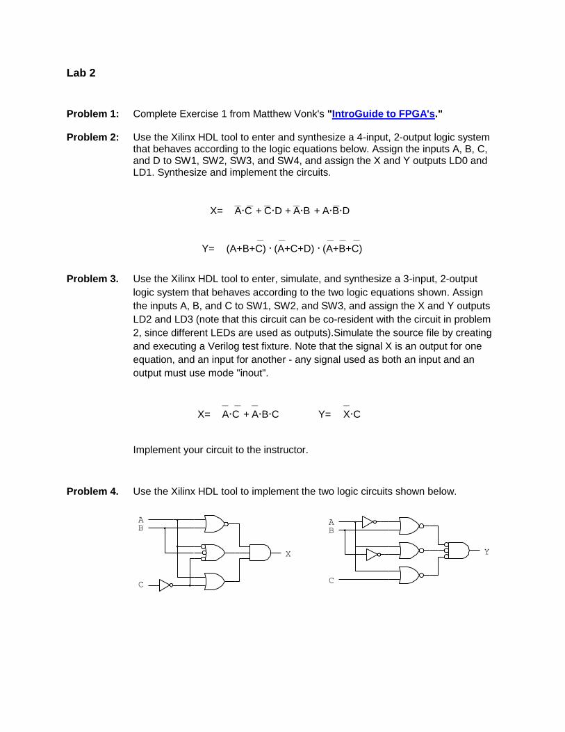
Problem 4. Use the Xilinx HDL tool to implement the two logic circuits shown below.
X= AC + CD + AB + ABD __ __ __ __ __
__ __ __ __ __
Y= (A+B+C) (A+C+D) (A+B+C)
__ __ __ __
X= AC + ABC Y= XC
BA
C
X
BA
C
Y
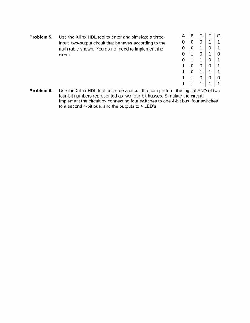
Problem 5. Use the Xilinx HDL tool to enter and simulate a three-
input, two-output circuit that behaves according to the
truth table shown. You do not need to implement the
circuit.
Problem 6. Use the Xilinx HDL tool to create a circuit that can perform the logical AND of two
four-bit numbers represented as two four-bit busses. Simulate the circuit. Implement the circuit by connecting four switches to one 4-bit bus, four switches to a second 4-bit bus, and the outputs to 4 LED’s.
A B C F G
0 0 0 1 1
0 0 1 0 1
0 1 0 1 0
0 1 1 0 1
1 0 0 0 1
1 0 1 1 1
1 1 0 0 0
1 1 1 1 1

Lab 3 This lab project presents several worded problems that serve as behavioral specifications for
digital circuits. Your job is to design, simulate, and download those circuits to your board.
Problem 1. Amy, Baker, Cathy, and David, the bean buyers for the "Overhead Coffee
Company", have designed a more complex voting system to decide when to buy
new beans. Design and implement a logic circuit that they can use to indicate
whether they should buy new beans. Use slide switches for vote entry (either
"buy" or "not buy"), and an LED to indicate when beans should be purchased. A
“buy” order is placed if:
Amy, Cathy, and David vote NO and Baker votes YES,
or Amy and David vote NO and the rest vote YES,
or Baker and David vote YES and the rest vote NO,
or Amy votes NO and the others vote YES,
or Baker votes NO and the others vote YES,
or Baker and Amy vote YES and the others vote NO,
or Cathy votes NO and the others vote YES,
or David votes NO and the others vote YES,
or Amy and Cathy vote YES and the others vote NO,
or they all vote YES.
Implement your circuit.
Problem 2. Define and simulate a circuit that can detect all prime numbers less than 16.
Assume that the four inputs to your circuit (B3B2B1B0) are used to form a four-bit
binary number in the range 0 to 15. Your circuit should illuminate an LED
whenever the input binary number is a prime number. One way to solve this
problem is to create a truth-table or K-map, and then place a '1' in the
appropriate row or cell to indicate a prime number. Verify your circuit's behavior
through simulation, then synthesize and download it to your board. Use four slide
switches as inputs, and a single LED as output. Note that this circuit can co-
reside in your board with the previous problem if you use a different LED for the
output.
Problem 3. Use twelve 1’s in three groups of four cells to specify a 5-input, one output circuit
to serve as your K-map battleship field in the diagram below. You may want to
print additional copies of the K-map to practice designing a circuit that you think
will be the hardest to guess. Find a minimum circuit, and enter and simulate it
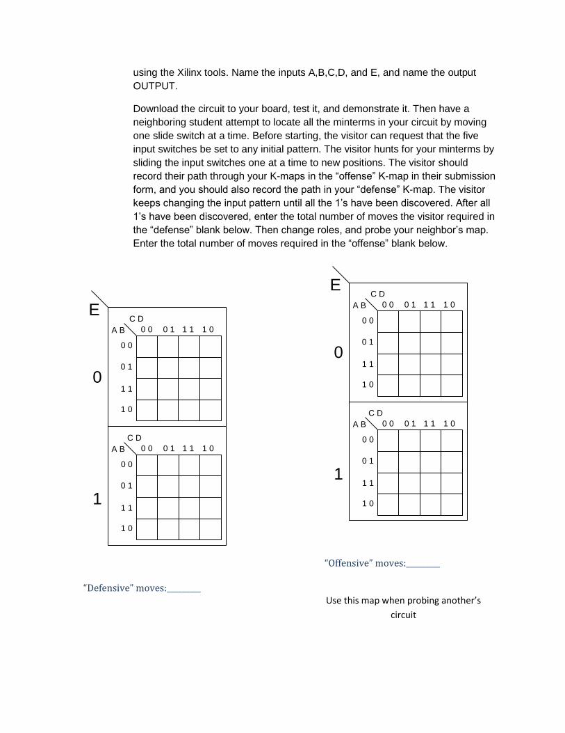
using the Xilinx tools. Name the inputs A,B,C,D, and E, and name the output
OUTPUT.
Download the circuit to your board, test it, and demonstrate it. Then have a
neighboring student attempt to locate all the minterms in your circuit by moving
one slide switch at a time. Before starting, the visitor can request that the five
input switches be set to any initial pattern. The visitor hunts for your minterms by
sliding the input switches one at a time to new positions. The visitor should
record their path through your K-maps in the “offense” K-map in their submission
form, and you should also record the path in your “defense” K-map. The visitor
keeps changing the input pattern until all the 1’s have been discovered. After all
1’s have been discovered, enter the total number of moves the visitor required in
the “defense” blank below. Then change roles, and probe your neighbor’s map.
Enter the total number of moves required in the “offense” blank below.
A B
C D
0 0 0 1 1 1 1 0
0 0
0 1
1 1
1 0
A B
C D
0 0 0 1 1 1 1 0
0 0
0 1
1 1
1 0
E
0
1
“Defensive” moves:_________
Use this map when someone else is
probing your circuit
A B
C D
0 0 0 1 1 1 1 0
0 0
0 1
1 1
1 0
A B
C D
0 0 0 1 1 1 1 0
0 0
0 1
1 1
1 0
E
0
1
“Offensive” moves:_________
Use this map when probing another’s
circuit

Lab 4 This lab project presents several more complex combinational logic systems that would be quite
challenging to implement using structural methods, but are rather simple using Verilog.
Problem 1: Six judges need a device to help indicate particular judgments. Each judge can
enter “good” or “bad” with a single switch - you job is to build a circuit that can indicate three separate conditions: A strong majority (i.e., 5 or 6 “good” votes); a simple majority (4 or more “good” votes), and a tie (exactly 3 “good” votes). Use LEDs to indicate the outputs.
Problem 2. A digital thermometer produces a continuously varying voltage signal between
0V and 5V, where 0V represents 0 degrees, and 5V represents 100 degrees.
The thermometer outputs an 8-bit binary number proportional to the temperature
– “00000000” represents 0 degrees, each increasing binary number from
“00000000” represents a temperature increase of 100/256 degrees, and
“11111111” represents 100 degrees. Design a circuit that outputs a logic high
signal whenever the temperature is between 50 and 60 degrees. Use switches to
emulate the thermometer's output, and an LED to indicate when the temperature
is in the desired range.
Problem 3. Design a circuit that can show an 8-bit 2's complement number multiplied by -1.
Use the eight slide switches to enter any number (positive or negative), and show
the answer on the 8 LED's.

BC
A
00 01 11 10
0 D D or E E xor F E xnor F
1 not D D nand E 1 0
Lab 5
Problem 1. Create a Verilog source file for a circuit that behaves according to the
requirements shown by the K-map below. Simulate the circuit using a Verilog test
fixture.
Problem 2. Design, simulate and implement a mux/de-mux circuit using the Xilinx tools and
the Digilent board that can communicate 8 data signals using only 4 wires (1 data
wire, and three bits to select one signal out of 8). Use three buttons to select the
data channel, slide switches to form the eight required data channel inputs, and 8
LEDs to show the output. An LED is lit only if the corresponding channel is
selected AND the corresponding switch is HIGH.
Problem 3. Design and implement a “bin2hex” seven-segment decoder circuit that can drive a single digit on the 4-digit 7sd device on the Digilent board (you are not required to simulate this circuit). Your decoder should display the decimal digits 0-9 for bit patterns 0000-1001, and A-F for bit patterns 1010-1111 (you will need to get a little bit creative to show all the hex digits – think about lower-case letters). Use four slide switches as inputs to select the pattern to be displayed. Recall you will need to drive the anode signal of the digit you wish to use to 3.3 V (you can drive the others to GND to ensure they are off – note that if you drive all anode signals to 3.3 V, then all four digits will show the same pattern). (Note: The circuits for Problems 3 and 4 can both be loaded into the board at the same time, if you wish).
Problem 4. Adding to your circuit from Problem 3, create a circuit that can drive a second
digit on the 7sd device with a new digit pattern defined by the other four slide switches on your board. Since there are only seven signals available to drive the digit segments, you need only one bin2hex component to drive those signals, and a 2:1 "bus multiplexor" to choose which set of switches are connected to the bin2hex component. The signal used select which switches drive the display can also be used to select which digit is enabled - using the same signal for both purposes ensures the correct data will always appear on the same display digit. A pushbutton can be used to drive the select signal.

Switches(3:0)
Switches(7:4)
AN0 AN2 AN3AN1
4
CA
CB
CC
CD
CE
CF
CG
A ‘0’ on AN2 and
AN3 turns these
digits off
The inverter allows a single digit to be driven at any time
Push-
button
2:1 Bus
Mux
bin2hex
S0
1
See if you can toggle the button quickly enough to make both displays appear continually illuminated (it is unlikely you will be able to do so). Imagine that you could toggle the button very quickly - faster than about 50 times per second. Each digit would appear to be continuously illuminated, even though each was really only driven for half the time. This works because the light-sensing apparatus in the human eye becomes "saturated" after only a few microseconds, and several milliseconds are required before the eye can respond to new stimulus. We will exploit this even further in Lab 9, where we will use a "sequential circuit" to build a circuit capable of driving all four digits.
Problem 5. Use the Xilinx tools to define and simulate an 8-bit shifter that can shift or rotate
left or right by 0, 1, 2, or 3 bit positions. Implement the circuit using the 8 slide switches as inputs to the shifter, and 8 LEDs as outputs from the shifter. Use the pushbuttons to control the functions of the shifter.

Lab 6 Problem 1. Design and simulate an 8-bit magnitude comparator.
Problem 2. Design and simulate a structural 8-bit adder, using a behavioral HA component
and seven behavioral FA components. ("Structural" means that you're creating
the desired behavior by assembling smaller components; you're not simply
describing the overall behavior with a + operator.)
Problem 3. Design and simulate a behavioral 8-bit adder that can produce a 9-bit result.
Show a case where the ninth bit is a '1'.
Problem 4: Implement a structural 4-bit adder/subtractor module. Use four slide switches to
set the A operand, four slide switches to set the B operand, and a pushbutton to
select add or subtract. Use five LEDs for circuit output. Check enough cases to
be sure your circuit works.
Problem 5: Design an underflow/overflow detect circuit that does not need to access the
carry-in signal to the most-significant bit, and add that circuit to your design from
problem 4. Drive an LED to show when an output is in error.
Problem 6. Implement a structural 4-bit multiplier using your HA, FA, and 8-bit behavioral adder as components. Simulate the multiplier using several representative cases stored in a test bench waveform file. Use eight slide switches as inputs (four switches per input) and the eight LED’s as outputs.

Problem 7: Design and implement a 4-bit ALU that can perform the operations shown. Assign inputs to slide switches and pushbuttons as you see fit, and assign outputs to LEDs or the 7sd.
Op Code Function
000 A PLUS B
001 A PLUS 1
010 A MINUS B
011 A MINUS 1
100 A XOR B
101 Not A
110 A OR B
111 A AND B

Lab 7
Problem 1. Implement the function Y = A’.B + A.C. Define the NOT, OR and two AND operations separately, and give each operation a 1ns delay. Simulate the circuit with all possible combinations of inputs. Answer the questions below.
Observe the outputs of the AND gates and the overall circuit output when B and C are both high, and A transitions from H to L and then from L to H (you may want to create another simulation to focus on this behavior). What output behavior do you notice when A transitions? What happens when A transitions and B or C are held at ‘0’?
How long is the output glitch? ______ Is it positive ( ) or negative ( ) (circle one)? Change the delay through the inverter to 2ns, and resimulate. Now how long is output glitch? ______ What can you say about the relationship between the inverter gate delay and the length of the timing glitch?
Based on this simple experiment, an SOP circuit can exhibit positive/negative glitches (circle one) when an input that arrives at one AND gate in a complemented form and another AND gate in uncomplemented form transitions from a _____ to a _____.
Problem 2. Enter the logic equation from problem 1 in the K-map below, and loop the
equation with redundant term included. Add the redundant term to the Xilinx circuit, re-simulate, and answer the questions.
B C A
00
01
11
10
0
1
F
Did adding the new gate to the circuit change the logical behavior of the circuit?
What effect did the new gate have on the output, particularly when A changes and B and C are both held high?
FSOP (original):
F SOP (new):

BC
A
00 01 11 10
A 0
1
F
Problem 3. Create a three-input POS circuit to illustrate the formation of a glitch. Drive the simulator to illustrate a glitch in the POS circuit, and answer the questions below.
A POS circuit can exhibit a positive/negative glitch (circle one) when an input that arrives at one OR gate in a complemented form and another OR gate in un-complemented form transitions from a _____ to a _____.
Write the POS equation you used to show the glitch:
Enter the equation in the K-map below, loop the original equation with the redundant term, add the redundant gate to your Xilinx circuit, and resimulate.
How did adding the new gate to the circuit change the logical behavior of the circuit?
What effect did the new gate have on the output, particularly when A changes and B and C are both held high?
Problem 4. Copy the SOP circuit above to a new file, and increase the delay of the output
OR gate. Simulate the circuit and answer the questions below.
How did adding delay to the output gate change the output transition? Does adding delay to the output gate change the circuit’s glitch behavior in any way?
F POS (new):

Problem 5. Create a circuit for Z = (A.B) . (A.C)'. Change the delay of the AND gate to 1ns and the NAND gate to 2ns. Simulate the circuit, inspect the output, and answer the questions below.
What kind of glitch did you observe? What input conditions are required for the glitch to form?
How long was the glitch, and how is its length related to timing delays in the AND and NAND gates?
Problem 6. Design and implement an 8-bit adder. Simulate the circuit in post-route mode
(select Simulation, then change "Behavioral to "Post-Route"), then have the instructor inspect your simulation output.
How long does it take for the adder result to be valid after the inputs change?
______ What is the maximum frequency this circuit could run at? _____

Lab 8 Problem 1. Create a NAND basic cell in the Xilinx tools using structural methods. Add a 1ns
gate delay to both NAND gates (for both rising and falling transitions). Label inputs S and R and the outputs Q and QN as appropriate. Create a test fixture to simulate the circuit, driving the inputs as specified below.
De-assert both inputs at the start of the simulation. At 100ns, asset S. At 200ns, de-assert S. At 300ns, assert R. At 400ns, de-assert R. At 500ns, assert both inputs. At 600ns, de-assert both inputs. At 700ns, assert both inputs. Identify the output features in the list below.
1. An undefined output 2. A set operation 3. A reset operation 4. A ‘0’ being stored in memory 5. A ‘1’ being stored in memory 6. A state where the Q and QN outputs are both driven to the same
value 7. A metastable state
Problem 2. Repeat problem 1, but use a NOR basic cell. Why are the basic cells outputs
undefined at the start of the simulation?
Complete the following table by placing the correct letter in the output column: A: set operation; B: reset operation; C: confounded outputs (both outputs at the same voltage); D: storing a value in memory; E: a metastable state.
Problem 3. Modify the test bench for the NAND basic cell by de-asserting S at 600ns and R
at 601ns, and resimulate. Comment on any differences in the output, and more importantly, give a reason for any differences seen.
Set Reset NAND Output NOR output
1 0 1 1
1 1 1 0
1 1 1 1
1 0 1 0
0 1 0 1
0 0 0 0
0 0 0 1
0 1 0 0

Problem 4. Starting with the NAND basic cell, create a new source file for a D-latch. Be sure the basic cell NAND gates have a 1ns gate delay. Simulate this circuit, and be sure to test all possible combinations of inputs to fully document the circuit’s function. At some point during the simulation, illustrate the property of D-latch transparency (i.e., show the circuit behavior when gate input is high, and the D input changes from L-H-L or H-L-H), and also illustrate a metastable state. Observe on the simulation waveform the following output behaviors: an undefined output, transparency, storing a ‘1’, storing a ‘0’, and metastability.
Problem 5. Create a behavioral source file for a rising-edge triggered D flip-flop. Name the
inputs D and CLK, and the output Q. Simulate the flip-flop, driving CLK and D appropriately. What do you notice about the output Q? Why?
Add an asynchronous reset, and assert the reset signal at the start of the simulation, de-asserting it after a small amount of time. Resimulate, and demonstrate the proper operation of your flip-flop. Modify the simulation, and try to force a metastable state. Can you force a metastable state?
Problem 6. Create a source file for a falling-edge triggered flip-flop with clock enable and preset. Simulate the FF, showing all pertinent operating states.
Problem 7. Create a source file for an 8-bit D register with both a synchronous reset (named
SRST) and an asynchronous reset (named ARST). Simulate the register, showing all pertinent operating states.
Problem 8: Create and simulate a source file for a T flip-flop. Show all pertinent operating
states in the simulation. Problem 9: Create and simulate a source file for a JK flip-flop.

Lab 9
Problem 1. Build a 4-bit binary counter with Enable and Terminal Count functions (Terminal
Count, or TC, is asserted in the last count state before the counter resets back to
all zeros). Simulate the counter, showing the TC and Enable functions.
Problem 2. Design a circuit that increments a digit (0 – F) shown on the seven-segment
display device once each second. The circuit has four pushbutton inputs: one
button starts the counter, a second button stops the counter, a third button
increments the counter, and the fourth button asynchronously resets all memory
devices in the design. The system has the block diagram shown below. Use the
4-bit counter from problem #1 as a component, and create components for a
clock divider, seven-segment display decoder, and a controller circuit.
Start
Controller
Stop
Inc
RSTClk
Run
4-bit counter
B0
B1
B2
B3
Cen
7-seg decoder
BTN1
BTN2
BTN3
BTN4
CA
CB
CC
CD
CE
CG
CF
RST
ClkClk pin
Clk divider
Problem 3. Build a 4-bit decimal counter with Enable and Terminal Count functions - you will
use this counter as a component in the next problem.
Problem 4. Build a 4-digit decimal stopwatch, with the least-significant digit counting a rate of
1KHz (1ms update rate), and the most-significant digit incrementing once per
second (each digit on the seven-segment display will be driven from a separate
decimal counter). Use the same controller as was used for Problem 2.
This circuit requires a scanning display controller which is discussed in your
board’s Reference Manual.
Lab 10
Problem 1. Create a circuit that displays the greatest common divisor of two four-bit numbers
read from a Verilog ROM (Example 68 from the book).
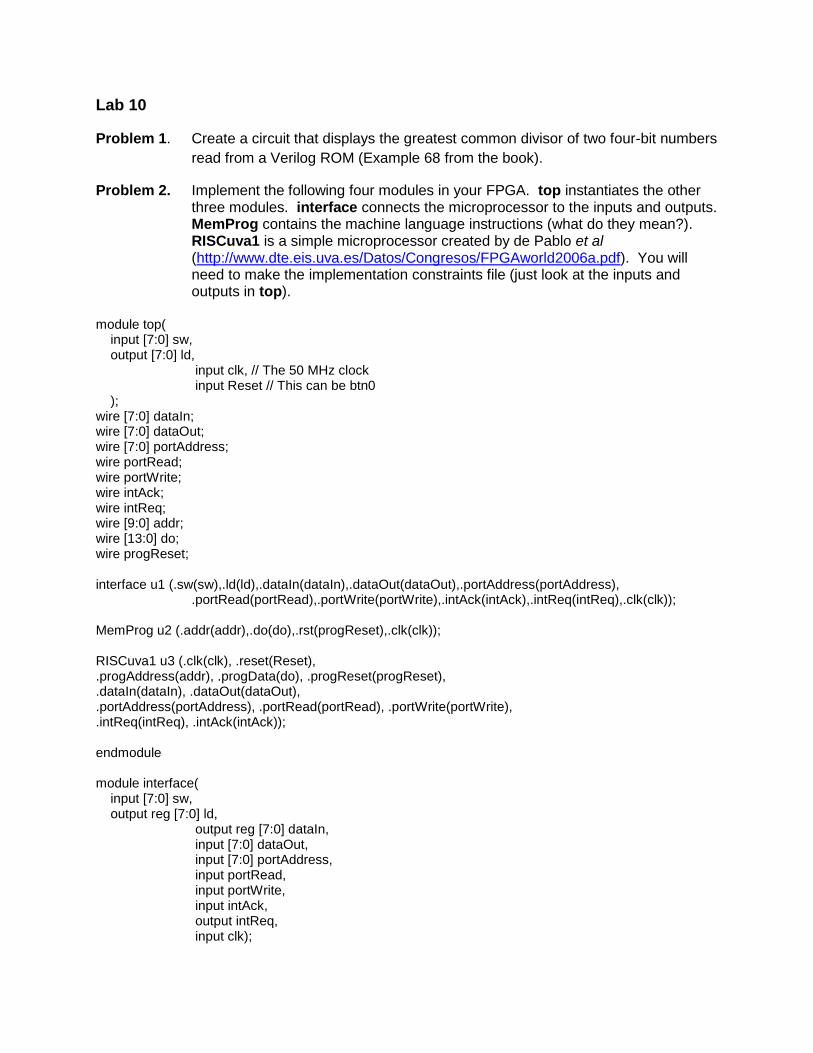
Problem 2. Implement the following four modules in your FPGA. top instantiates the other three modules. interface connects the microprocessor to the inputs and outputs. MemProg contains the machine language instructions (what do they mean?). RISCuva1 is a simple microprocessor created by de Pablo et al (http://www.dte.eis.uva.es/Datos/Congresos/FPGAworld2006a.pdf). You will need to make the implementation constraints file (just look at the inputs and outputs in top).
module top( input [7:0] sw, output [7:0] ld, input clk, // The 50 MHz clock input Reset // This can be btn0 ); wire [7:0] dataIn; wire [7:0] dataOut; wire [7:0] portAddress; wire portRead; wire portWrite; wire intAck; wire intReq; wire [9:0] addr; wire [13:0] do; wire progReset; interface u1 (.sw(sw),.ld(ld),.dataIn(dataIn),.dataOut(dataOut),.portAddress(portAddress), .portRead(portRead),.portWrite(portWrite),.intAck(intAck),.intReq(intReq),.clk(clk)); MemProg u2 (.addr(addr),.do(do),.rst(progReset),.clk(clk)); RISCuva1 u3 (.clk(clk), .reset(Reset), .progAddress(addr), .progData(do), .progReset(progReset), .dataIn(dataIn), .dataOut(dataOut), .portAddress(portAddress), .portRead(portRead), .portWrite(portWrite), .intReq(intReq), .intAck(intAck)); endmodule module interface( input [7:0] sw, output reg [7:0] ld, output reg [7:0] dataIn, input [7:0] dataOut, input [7:0] portAddress, input portRead, input portWrite, input intAck, output intReq, input clk);

always @(posedge clk) if ((portWrite==1)&(portAddress==225)) ld=dataOut; always@(*) if ((portRead==1)&(portAddress==224)) dataIn=sw; assign intReq=0; endmodule module MemProg(input [9:0] addr, output reg [13:0] do, input rst, input clk); always @ (posedge clk) if (rst==1) do<=14'b00000000000000; else case(addr) 0:do<=14'b11111000000000; 1:do<=14'b00111000010000; 2:do<=14'b00010000000000; endcase endmodule module RISCuva1 ( clk, reset, progAddress, progData, progReset, dataIn, dataOut, portAddress, portRead, portWrite, intReq, intAck ); // Inputs and outputs: input clk, reset; // Clock and Reset output [9:0] progAddress; // Up to 1K instructions (10 bits) input [13:0] progData; // Current instruction code output progReset; // Reset of Program Memory input [7:0] dataIn; // Data input (from an I/O port) output [7:0] dataOut; // Data output (through a port) output [7:0] portAddress; // Addressed I/O Port (0..255) output portRead; // Read signal output portWrite; // Write signal input intReq; // Interrupt request output intAck; // Interrupt Acknowledge // Instruction decoding from the instruction code: wire [13:0] opCode = progData; // Instruction code wire [1:0] opA = opCode[13:12]; // 1st operation code wire [1:0] opB = opCode[11:10]; // 2nd operation code wire [1:0] opC = opCode[ 9: 8]; // 3rd operation code wire [3:0] rM = opCode[ 7: 4]; // Source register wire [3:0] rN = opCode[ 3: 0]; // Destination register wire [9:0] immAddr = opCode[ 9:0]; // Address for jumps wire [7:0] immData = opCode[11:4]; // Immediate data wire [4:0] immPort = opCode[ 8:4]; // For direct access wire MISC = (opA == 2'b00); wire JP = (opA == 2'b01); wire LOAD = (opA == 2'b10); wire ALU = (opA == 2'b11); wire CALL = (opB == 2'b00);

wire GOTO = (opB == 2'b01); wire RETS = (opB == 2'b10); wire MOVOUT = (opB == 2'b11); wire RET = (opC == 2'b00); wire RETI = (opC == 2'b01); wire DI = (opC == 2'b10); wire EI = (opC == 2'b11); wire FLAG_Z = (opB == 2'b00); wire FLAG_NZ = (opB == 2'b01); wire FLAG_C = (opB == 2'b10); wire FLAG_NC = (opB == 2'b11); wire LOGIC = (opB == 2'b00); wire ARITH = (opB == 2'b01); wire SHIFT = (opB == 2'b10); wire MOVIN = (opB == 2'b11); wire MOV = (opC == 2'b00); wire XNOR = (opC == 2'b01); wire OR = (opC == 2'b10); wire AND = (opC == 2'b11); wire ADD = (opC == 2'b00); wire ADC = (opC == 2'b01); wire SUB = (opC == 2'b10); wire SBC = (opC == 2'b11); wire ASR = (opC == 2'b00); wire RRC = (opC == 2'b01); wire ROR = (opC == 2'b10); wire ROL = (opC == 2'b11); wire IND = (opC == 2'b00); wire SEQ = (opC == 2'b01); wire DIR = (opC >= 2'b10); // General Resources: reg zeroFlag, carryFlag; // DFFs used by flags wire [7:0] dataBus; // Data bus for all operations wire [2+9:0] stackValue; // Internal stack output // Register file (r0-r15) and operand buses: reg [7:0] registerFile[0:15]; // 16x8 dual-port memory always@(posedge clk) begin if (LOAD | ALU) registerFile[rN] <= dataBus; // Synchronous write end wire [7:0] busN = registerFile[rN]; // Async. read of rN wire [7:0] busM = registerFile[rM]; // Async. read of rM // Port signals for direct, indirect and sequential accesses: reg [7:0] nextPort; always@(posedge clk) begin if (portRead | portWrite) nextPort <= portAddress + 1; // For sequential use end assign dataOut = busN; // Output from rN assign portRead = ALU & MOVIN; // Read signal assign portWrite = MISC & MOVOUT; // Write signal assign portAddress = IND ? busM : // Indirect SEQ ? nextPort : // Sequent. {3'b111,immPort}; // Direct

// Logic ALU: AND, OR, XNOR and MOV. wire logicCarry = AND ? 1'b1 : OR ? 1'b0 : carryFlag; wire [7:0] logicALU = AND ? busN & busM : OR ? busN | busM : XNOR ? busN ~^ busM : busM ; // Arithmetic ALU: ADD, ADC, SUB and SBC. wire [7:0] arithALU, altM; wire arithCarry, x, y, z; assign x = ADD ? 1'b0 : ADC ? carryFlag : SUB ? 1'b1 : ~carryFlag; assign altM = (SUB | SBC) ? ~busM : busM; assign {z, arithALU, y} = {busN, 1'b1} + {altM, x}; assign arithCarry = (SUB | SBC) ? ~z : z; // Shifter: ASR, RRC, ROR and ROL. wire [7:0] shiftALU; wire shiftCarry; assign {shiftALU, shiftCarry} = ASR ? {busN[7], busN} : RRC ? {carryFlag, busN} : ROR ? {busN[0], busN} : {busN[6:0], busN[7], busN[7]}; // This data bus collects results from all sources: assign dataBus = (LOAD | MISC) ? immData : 8'bz; assign dataBus = (ALU | JP) & LOGIC ? logicALU : 8'bz; assign dataBus = (ALU | JP) & ARITH ? arithALU : 8'bz; assign dataBus = (ALU | JP) & SHIFT ? shiftALU : 8'bz; assign dataBus = (ALU | JP) & MOVIN ? dataIn : 8'bz; // Interrupt Controller: reg userEI, callingIRQ, intAck; wire mayIRQ = ! (MISC & RETS | MISC & MOVOUT | ALU & MOVIN); wire validIRQ = intReq & ~intAck & userEI & mayIRQ; wire [9:0] destIRQ = callingIRQ ? 10'h001 : 10'h000; always@(posedge clk or posedge reset) begin if (reset) userEI <= 0; else if (MISC & RETS & DI) userEI <= 0; else if (MISC & RETS & EI) userEI <= 1; if (reset) intAck <= 0; else if (validIRQ) intAck <= 1; else if (MISC & RETS & RETI) intAck <= 0; if (reset) callingIRQ <= 0; else callingIRQ <= validIRQ; end // Flag DFFs: always@(posedge clk) begin if (MISC & RETS & RETI) // Flags recovery when ‘reti’ {carryFlag,zeroFlag} <= stackValue[11:10]; else begin if (LOAD | ALU) // 'Z' changes with registers zeroFlag <= (dataBus == 8'h00); if (ALU & ~MOVIN) // but 'C' only with ALU ops carryFlag <= LOGIC ? logicCarry :

SHIFT ? shiftCarry : arithCarry ; end end // 'validFlag' evaluates one of four conditions for jumps. wire validFlag = FLAG_Z ? zeroFlag : FLAG_NZ ? ~zeroFlag : FLAG_C ? carryFlag : ~carryFlag ; // Program Counter (PC): the address of current instruction. reg [9:0] PC; wire [9:0] nextPC, incrPC; wire onRet = MISC & RETS & (RETI|RET); wire onJump = MISC & (GOTO | CALL) | JP & validFlag; assign incrPC = PC + (callingIRQ ? 0 : 1); assign nextPC = onRet ? stackValue[9:0] : 10'bz; assign nextPC = onJump ? immAddr | destIRQ : 10'bz; assign nextPC = !(onRet | onJump) ? incrPC : 10'bz; always@(posedge clk) begin PC <= nextPC; end // When using Xilinx BlockRAM as program memory: assign progAddress = nextPC; assign progReset = reset | validIRQ; // Internal stack for returning addresses (16 levels): reg [3:0] SP; // Stack Pointer register always@(posedge clk or posedge reset) begin if (reset) SP <= 0; else if (MISC & CALL) SP <= SP + 1; else if (MISC & RETS & (RETI|RET)) SP <= SP - 1; end wire [3:0] mySP = (CALL | GOTO) ? SP : SP - 1; reg [2+9:0] stackMem[0:15]; // Stack 16x12 memory always@(posedge clk) begin if (MISC & CALL) // Keep returning address and flags stackMem [mySP] <= {carryFlag, zeroFlag, incrPC}; end assign stackValue = stackMem[mySP]; endmodule /// RISCuva1 (all in one file!)
Problem 3. Modify the instructions in MemProg so that the output will equal the input plus 1.
You will need to store the number 1 in a register and then add.
Problem 4. Now modify the instructions so that the output equals the slide-switch input
unless BTN1 is pushed, in which case the output becomes 0. You will need to
modify top (adding an input) and interface. You must assign BTN1 (preceded
by 7 zeros) a different port number than the slide switches.