Embed Size (px)
Citation preview

Design with Microprocessors (DMP) – Lab. 2
1
Laboratory 2 – applications with simple I/O modules.
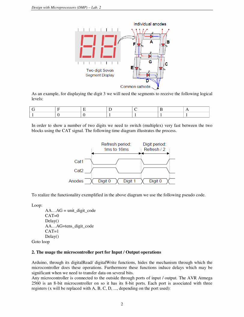
1. The 2x7 segment display
The PmodSSD (Seven Segment Display) from the figure bellow provides the possibility of displaying two characters. Each segment is a LED, which gives light if there is the right
combination of voltages on the segments anode and cathode (anode High, cathode LOW).
In order to reduce the number of pins necessary, the two digits cannot be lit simultaneously.
The selection between the two digits is done by the CAT signal (the C on the schema below). If this
signal is 0 the segments corresponding to the unities are giving light and if the CAT signal is 1 the
segments corresponding to the digit on the left are lit.
The signs denoted by the letters AA…AC correspond to the anodes of the segment LEDs.
The correspondence of these signals is indicated by the figure bellow:
Design with Microprocessors (DMP) – Lab. 2
2
As an example, for displaying the digit 3 we will need the segments to receive the following logical levels:
G F E D C B A
1 0 0 1 1 1 1
In order to show a number of two digits we need to switch (multiplex) very fast between the two
blocks using the CAT signal. The following time diagram illustrates the process.
To realize the functionality exemplified in the above diagram we use the following pseudo code.
Loop:
AA…AG = unit_digit_code
CAT=0
Delay()
AA…AG=tens_digit_code
CAT=1
Delay()
Goto loop
2. The usage the microcontroller port for Input / Output operations
Arduino, through its digitalRead/ digitalWrite functions, hides the mechanism through which the microcontroller does these operations. Furthermore these functions induce delays which may be
significant when we need to transfer data on several bits. Any microcontroller is connected to the outside through ports of input / output. The AVR Atmega
2560 is an 8-bit microcontroller on so it has its 8-bit ports. Each port is associated with three registers (x will be replaced with A, B, C, D, ..., depending on the port used):

Design with Microprocessors (DMP) – Lab. 2
3
– DDRx – direction reister
– PORTx – output register – PINx – register for input data
The direction register DDRx
DDRx (Data Direction Register) configures the data direction of the port pins (if a bit of a
port will be used for input or output). A written on a bit of 0 makes the pin DDRx
port corresponding to the input pin, and a bit set to 1 makes the corresponding pin to be
output pin.
Examples:
• In order to configure all the bits port A as input pins DDRA = 0b00000000;
• To configure all the bits of port A as output DDRA = 0b11111111;
• To configure the lower half of port B as output and the upper half as input DDRB = 0b00001111;
The input register PINx PINx (Port IN) is used to read data from the set the set of pins configured as input. To read data, these pins
must be set as input pins, setting all of DDRx bits to zero. Example: reading data from port A:
DDRA = 0; char a = PINA;
The output register PORTx
Register PORTx is used to transmit data to the microcontroller peripherals connected to the port x pins. For data output to be visible, corresponding bits of DDRx register must be set the direction of
value 1. Example: switching on half of the 8 LEDs connected to Port A DDRA = 0xFF
PORTA = 0b10101010
3. Connecting the Seven Segments display to the Arduino board
The assembly is done with the board unplugged from the PC. The first step is the introduction
of the display into the breadboard, gently without hitting or damaging the system. Then we will
connect the power wires in the half-columns corresponding to GND and VCC for the second
connector (J2) of the display. The other end of the powering wires will be connected to the 5V and
GND pins of the Arduino board. We are not required to apply extra voltage to the J1 connector.
For the wires corresponding to the anodes of the display AA…AG and for the cathode CAT, we
will connect successively wires that we will introduce into Arduinos digital pins starting from
position 22, 23,…29, corresponding to bits 0…7 of port A.
The integral assembly:

Design with Microprocessors (DMP) – Lab. 2
4
Details of how the wires are connected:
The connection of the signal wires:

Design with Microprocessors (DMP) – Lab. 2
5
Please Note:
The first two pins of the connector from the Arduino board are power pins. The digital pins
start from the second pair. Pay much attention of their position.
Create a new project (sketch) in Arduino, and copy the following code:
// Display on SSD
// connected at PORTA
// Table of values, or look up table (LUT) with the BCD codes for every digit from 0 to 9. Every bit
corresponds to a LED, 1 means the LED is lit and 0 means it is not giving light.
const unsigned char ssdlut[] = {0b00111111, 0b00000110, 0b01011011, 0b01001111, 0b01100110,
0b01101101, 0b01111101, 0b00000111, 0b01111111, 0b01101111};
// the size of the lut
const int lutsize = 10;
int cpos = 0; // current position
int cdigit = 0; // first digit from the two
unsigned char outvalue = 0;
void setup() { // setting port A as output
DDRA = 0b11111111; }
void loop() {
outvalue = cdigit>0 ? 0x80 : 0;
// which cathode are we choosing ? (00000000 sau 10000000)
// the cathode is wired to bit7 from port A, through this operation we are setting bit 7 on logical 1 or
//0, alternatively, the following bits will be attached through a logical OR operation in the following
//line of code
PORTA = (ssdlut[cpos] | outvalue); // we make an OR between the value from the LUT and the
selected cathode
cpos++; // we increment the current position
if (cpos>=lutsize) { // if we reached the final position
cpos = 0; // we come back at 0 cdigit^=1; // if the previus digit was 0 we make it a 1 and vice versa
}
// wait 0.5 sec delay(500);
}
This small program will display the digits from 0 to 9 on the first element and then do the same on
the second.

Design with Microprocessors (DMP) – Lab. 2
6
4. The Arduino Learning Shield
The „shields” are PCBs (Printed Circuit Boards) that can be placed over the Arduino boards, extending their capabilities. There is a large variety of shields, such as XBee shield, SD-Shield, H-
Bridge shield, etc. The mapping between the Arduino pins and the devices present on the shields should be carefully taken into account in when programming for proper mapping and conflicts
avoidance (the pins provided/used by the shield are specified in the product datasheet).
In this lab work we will use a learning shield, as seen in the figure below. The shield provides the
following resources:
- 1 seven segment display, with 4 digits
- 3 buttons (+ one reset button)
- 4 Leds
- 1 potentiometer for generating an analog signal
- 1 sound generator (buzzer)
The electric schematic for this shield can be downloaded from:
https://ardushop.ro/en/index.php?controller=attachment&id_attachment=40
Accessing the shield’s resources:
The buttons are connected to pins A1, A2 and A3. These buttons have pull-up resistors on the shield, and therefore their released state will generate a logic 1, and the pressed state will
generate a logic 0. There is no need for internal pull-up resistor activation.
The Leds are connected with the anode to VCC, and with the cathodes to pins 10, 11, 12
and 13. Thus, for lighting an LED a logic 0 must be written to the corresponding pin.
The 4x7 segments display is organized in a common anode configuration, with individual
cathodes for each digit segment, unlike the PMod SSD, where the segments have a common
cathode and separate anodes. Therefore, for lighting a digit we need to set the digit’s anode to logic
1, and the cathodes for the segments to be lit to zero.
For driving the four digits we’ll thus need 4 signals for the anodes, and 8 signals for the
cathodes (7 segments and the dot). These signals are not available for the programmer, but are
connected to two shift registers, as shown in the schematic below. The shift registers are connected
in series, the output of the anode register being connected with the input for the cathode register. As
a consequence, for writing a full configuration (selection of active digit + selection of segments to
light), only three signals are needed: - SDI – serial data in, connected to pin 8

Design with Microprocessors (DMP) – Lab. 2
7
- SFTCLK – shift clock, the clock signal for the data shifting, connected to pin 7
- LCHCLK – latch clock pin, the signal that allows reading the data, connected to pin 4.
For writing a digit, first the 8 bit cathode configuration must be transmitted, followed by 8 bits for
the anode configuration (with only one bit set to 1, for the active digit).
The following code is an example for using the 4x7 segment display:
int latchPin = 4; int clockPin =7;
int dataPin = 8; // SSD pins
const unsigned char ssdlut[] = {0b00111111, 0b00000110, 0b01011011, 0b01001111, 0b01100110,
0b01101101, 0b01111101, 0b00000111, 0b01111111, 0b01101111};
const unsigned char anodelut[] = {0b00000001, 0b00000010, 0b00000100, 0b00001000};
const unsigned char digits[] = {1,2,3,4}; // The number to be displayed is 1234. You can change it.
void setup ()
{
pinMode(latchPin,OUTPUT);
pinMode(clockPin,OUTPUT);
pinMode(dataPin,OUTPUT); // The three pins connected to the shift register must be output pins

Design with Microprocessors (DMP) – Lab. 2
8
}
void loop() {
for(char i=0; i<=3; i++) // For each of the 4 digits
{
unsigned char digit = digits[i]; // the current digit
unsigned char cathodes = ~ssdlut[digit]; // The cathodes of the current digit, we’ll negate the
value from the original LUT
digitalWrite(latchPin,LOW); // Activate the latch to allow writing
shiftOut(dataPin,clockPin,MSBFIRST, cathodes); // shift out the cathode byte
shiftOut(dataPin,clockPin,MSBFIRST, anodelut [i] ); // shift out the anode byte
digitalWrite(latchPin,HIGH); // De-activate the latch signal
delay(2); // Short wait
}
}
Analyzing the code:
- We will use the same LUT as in the previous example, but we have to complement the bits,
as now the bits activate the cathodes, on logic 0. - Arduino provides the function shiftOut, which transmits serially a byte on the dataPin,
generating a clock signal on clockPin. This function can be used with any two digital pins.
There are two ways of shifting out a byte: starting from bit 7 (MSBFIRST), or starting from
bit 0 (LSBFIRST). In our case, the MSBFIRST mode must be chosen, as it is important that
the bits of the cathodes correspond to the segments of the digits.
Results of running the program:

Design with Microprocessors (DMP) – Lab. 2
9
Individual Work
1) Build and run the first example from the document. 2) Fill in the LUT with the corresponding values for hexadecimal numbers (A,B,C,D,E). Test
the program with these kind of numbers. 3) Change the program so that you can show any number from 0 to 99 on the display, in a
decimal format. Take into account that it is not the same as its representation as digits on
half of byte (this thing is true in the case of hexadecimal numbers). For example, the number
16 is represented binary as 00010000, which will lead to the display of number 10. For
correctly displaying the decimal numbers the following steps will need to be realized:
-find the tens digit = the quotient from the division with 10
-find the unit digit = the remainder from the division with 10
CZ = nr div 10
CU = nr mod 10 = nr – (CZ*10)
4) Run the second example, using the Learning Shield.
5) Change the second example, to display any 4-digit decimal number. The number is provided
as int, not as individual digits. Make the number increment periodically. 6) Use the buttons on the Learning Shield. Use one button to increment the displayed number,
and another to decrement it. 7) Use the 4 digit display, and the buttons (on the Learning Shield) to make a chronometer that
counts seconds (2 digits) and hundredths of seconds (2 digits). Use one button for start, another for stop, and another for clear. Hint: use the function millis().