Embed Size (px)
Citation preview

FUJITSU SEMICONDUCTORDATA SHEET DS411-00004-0v02-E
ASSPISO/IEC 15693 Compliant FRAM EmbeddedHigh-speed RFID LSI
MB89R112
■ DESCRIPTIONThe MB89R112 is a vicinity type of RFID LSI device embedded with 9 Kbytes FRAM, which enables fastand frequent write operation.
■ FEATURES• Memory capacity of 9 Kbytes FRAM (including 8192 bytes of user area)• 32-byte/block configuration, 256 blocks• High-speed data transmission at 26.48 kbps• Fast command supported (data transmission at 52.97 kbps) (Transponder → Reader/Writer) • Carrier frequency at 13.56 MHz• Anti-collision function : 30 tags per second• Read/Write endurance : 1012 times• Data retention : 10 years ( + 85 °C) , 30 years ( + 70 °C)• 64-bit UID• FRAM memory data protection• Compliance with ISO/IEC 15693 (partly not supported*) • Compliance with ISO/IEC 18000-3 (Mode 1) (partly not supported*) • Serial Interface(SPI)
- Accessible area: User memory area can be read/written through SPI.- Access control with RF interface is prioritized- Power supply : 3.3 V (power is required for the memory access via SPI.)- Low power consumption: Operating current = 97 μA@2 MHz (Typ)
Standby current = 25 μA (Typ)- Power down mode: Power down current = 10 nA (Typ)- Package: 24-pin QFN (LCC-24P-M64)
* : Refer to “■USAGE NOTES”.
Note : FerVID family is a trademark of Fujitsu Semiconductor Limited, Japan.
TM
Copyright©2013 FUJITSU SEMICONDUCTOR LIMITED All rights reserved2013.5

MB89R112
■ BLOCK DIAGRAM
■ PIN ASSIGNMENT
Pin Number Pin Name Interface Direction Function Description
1 to 2 NC ⎯ ⎯ No connection pins (There is no internal connection.)
3 VSS Serial ⎯ Ground pin
4 VDD Serial ⎯ Supply Voltage pin
5 to 12 NC ⎯ ⎯ No connection pins (There is no internal connection.)
13 PWRP RF I/O Antenna pin
14 to 17 NC ⎯ ⎯ No connection pins (There is no internal connection.)
18 PWRM RF I/O Antenna pin
19 BUSY Serial O RF interface status pin
20 SPI Serial I SPI mode switch pin
21 SO Serial O Serial data output pin
22 SI Serial I Serial data input pin
23 SCK Serial I Serial clock pin
24 XCS Serial I Chip select pin
VDDVDD
R/W R/W
FRAMAnalog RF interface Digital control
Rectifier
Clock generator
Power supply voltage control
Modulator
Demodulator
SPI interface
I/O
Commands
FRAM access
Anti-collisionfunction
9 Kbytes
I/O
Commands
FRAM access
Converter
Clock
Data output
Data input
Data output
Data input Data output
Data input
Data output
Data input
Clock
Antenna
(TOP VIEW)
(LCC-24P-M64)
18 17 16 15 14 13
1 2 3 4 5 6
12
11
10
9
8
7
19
20
21
22
23
24
2 DS411-00004-0v02-E

MB89R112
■ RF INTERFACERF signal interface is compliant with ISO/IEC 15693.
■ SERIAL INTERFACEThis LSI has SPI (Serial Peripheral Interface) interface. It is able to access FRAM User memory through theSPI interface. In this case, the external power supply is required.
1. Pin Function Description
The Serial Pin and its function descriptions are shown in the table below.
• Pin function
Pin Number Pin Name Function Description
19 BUSY
RF Interface StatusWhen the VDD pin is set to ON during RF communication, BUSY will output “H”. In this status, serial communication will be ignored even if RF and serial communi-cations are both being performed at the same time, because the chip can only per-form RF communication when BUSY outputs “H”. Switching to the serial communication can be performed only when BUSY is “L”.
20 SPISPI Mode Switch pinThis is an input pin to control to switch to Serial communication mode. When SPI is “H”, the LSI can be transferred to Serial communication mode.
24 XCS
Chip Select pinThis is an input pin to select chip. When XCS is “H”, device is deselect (standby status) as long as the LSI is not write status internally. And SO becomes High-Z. In this case, inputs from all pins other than the antenna pin are ignored. When XCS is "L", the chip will be in selected state (active). XCS must fall before inputting op-code.
23 SCKSerial Clock pinThis is a clock input pin to input/output serial data. SI is loaded synchronously to a rising edge. SO is output synchronously to a falling edge.
22 SISerial Data Input pinThis is an input pin of serial data. It inputs op-code, address, and writing data.
21 SOSerial Data Output pinThis is an output pin of serial data. Reading data of FRAM memory are output. It is High-Z during standby.
4 VDD Supply Voltage pin: 3.3 V
3 VSS Ground pin
DS411-00004-0v02-E 3
MB89R112
2. Connection to SPI Interface
This LSI works as a slave of SPI. It can be connected to the microcontroller equipped with SPI port as shownin the figure below.
The external SPI controller shall monitor the BUSY signal. When a BUSY signal is “H”, the controller shallwait until “L” before performing SPI communication. When a BUSY signal is “H” and serial communicationis performed, the serial communication shall be ignored.
3. SPI Mode
MB89R112 supports the SPI mode 0 (CPOL = 0, CPHA = 0), and SPI mode 3 (CPOL = 1, CPHA = 1).
VDD
SPI SPIXCS XCSSCK SCK
SI MOSI
SO MISOBUSY BUSY
VSS VSS
MB89R112 Controller (External SPI access circuit)
7 6 5 4 3 2 1 0
MSB LSB
XCS
SCK
SI
7 6 5 4 3 2 1 0
MSB LSB
XCS
SCK
SI
SPI mode 0
SPI mode 3
4 DS411-00004-0v02-E

MB89R112
4. Arbitration between RF and SPI communication
This LSI has an access arbitration feature when there is access from both RF I/F and SPI I/F simultaneously.In this case, RF communication has priority. BUSY signal indicates that there is access from RF I/F, and it is validated when VDD is connected.
The controller needs to confirm the BUSY signal before changing to the SPI communication mode. Whenthe BUSY signal is in “H”, the SPI communication is ignored if the SPI communication is performed at thesame time because the LSI is executing RF communication. The BUSY pin outputs “H” if the VDD pin is turned on during RF communication as the figure shown below.
• Arbitration between RF and SPI communication
High-Z High-Z High-Z High-Z High-Z
SPISPI RFRF SPI
VDD
BUSY
SPI
XCS
SI/SCK
SO
Valid port
set to “L”
Internal rectificationpower supply
set to “L”
DS411-00004-0v02-E 5

MB89R112
5. Power Sequence in Serial Communication Mode
The power sequence in Serial communication mode is shown in the figure below.
After asserting VDD, check that BUSY is “L” and then assert SPI and XCS at the same time. Wait for 1 msor more after asserting XCS and then release XCS and begin serial communication. The timing specificationsfor the power sequence are shown in the following table. Refer to “■ COMMANDS OF SERIAL COMMUNI-CATION MODE” for details on the serial communication timing specifications.
• Serial communication power sequence
• Timing specifications during serial communication
Parameter Symbol Value (Min) Unit
SPI rising start time tSU 1000 μs
Power supply hold time tPH 0 μs
XCS level hold time at power ON tPU 1000 μs
XCS level hold time at power OFF tPD 0.06 μs
VDD
SPI
XCS
SCK/SI/SO
BUSY
tPU tPD
tSU tPH
Internal voltage
RF communication
set to “L”
set to “L”
set to “L”
(Refer to “■ COMMANDS OF SERIAL COMMUNICATION MODE”
for details)
Serial communication
6 DS411-00004-0v02-E

MB89R112
6. XCS Level Hold Time at Power ON/OFF
Power ON/OFF sequence while switching to the serial communication is shown in the figure below and XCSlevel hold time at power ON/OFF is shown in the table below.
If VDD falls down below 2.0 V, VDD is required to be started from 0 V to prevent malfunctions when the poweris turned on again.
• Power ON/OFF sequence in serial communication
If the device does not operate within the specified conditions of read cycle, write cycle or power on/offsequence, memory data can not be guaranteed.
Parameter SymbolValue
UnitMin Max
XCS level hold time at power OFF tpd 0.06 ⎯ μs
XCS level hold time at power ON tpu 1000 ⎯ μs
Power supply falling time tpi 10 ms
Power supply rising time trs 0.05 2 ms
VSS
XCS > VDD × 0.8* XCS > VDD × 0.8*
tpd tpu
trs
VIL (Max)
1.0 V
VIH (Min)
3.0 V
VDD
XCS : Don't careXCS XCS
VSS
VIL (Max)
1.0 V
VIH (Min)
3.0 V
VDD
tpi
*: XCS (Max)< VDD + 0.5 V
DS411-00004-0v02-E 7

MB89R112
■ MEMORY1. Memory Map
This section describes the FRAM memory, which is the internal memory of the MB89R112.
• FRAM Configuration
The FRAM has 8192 bytes for use as user area and 1024 bytes for use as system area. The user areas consist of 256 blocks. Each block can store 256 bits (32 bytes) of data.The block is the unit used for the writing and reading of FRAM data. The memory configuration of FRAM isshown below.
• FRAM memory configuration
• Lock Area
The following figure shows the area of Block Security Status and Read Lock Status of RF communicationcommand, SPI Read Lock and SPI Write Lock of SPI communication command.
Lock Status “1” means “Locked”, and “0” means “Not locked”.
Area Block Number (RF)
Logical address (SPI) Details
Access
RF communication
SPI communication
User area (8192 bytes)
00H to FFH (1block = 256bit)
0000H to 0FFFH (1address = 16bit)
User area Read/Write Read/Write
System area (1024 bytes)
Refer to “• Lock Area” for details. ⎯ Read
11EH 11E0H to 11EEHAFI, DSFID ⎯ Read
UID ⎯ Read
Block Number (RF)
Logical address(SPI) MSB LSB
RF lock status
BSS (Block
Security Status)
100H
1000H 0F 0E 0D · · · 03 2 1 01001H 1F 1E 1D · · · 13 12 11 10
1002H to 100EH EF to 20100FH FF FE FD · · · F3 F2 F1 F0
RLS (Read Lock
Status)101H
1010H 0F OE 0D · · · 03 2 1 01011H 1F 1E 1D · · · 13 12 11 10
1012H to 101EH EF to 20101FH FF FE FD · · · F3 F2 F1 F0
Serial lock
status
SRL (SPI Read
Lock)102H
1020H 0F 0E 0D · · · 03 2 1 01021H 1F 1E 1D · · · 13 12 11 10
1022H to 102EH EF to 20102FH FF FE FD · · · F3 F2 F1 F0
SWL (SPI Write
Lock)103H
1030H 0F 0E 0D · · · 03 2 1 01031H 1F 1E 1D · · · 13 12 11 10
1032H to 103EH EF to 20103FH FF FE FD · · · F3 F2 F1 F0
8 DS411-00004-0v02-E

MB89R112
• Data allocation in a block
Blocks “00H” to “FFH” are user area. The user area is defined as an area that can be accessed when thecorresponding block address is specified. The system area is defined as an area that can be accessed onlywith a specific command.
The system area contains UID, AFI, DSFID, and security status (can write or cannot write) data for individualblock. UID is fixed and cannot be updated. AFI and DSFID are written at the factory, and can be updatedand locked (disable to write) with commands.
RF 1block (32 byte) data allocation
Area Block Number(RF)
Logical address(SPI)
Logical address Data
(1addres = 16bit) 15 0
User area(8192 bytes)
00H 0000H to 000FH 0000H [15:0]
block0
10H 0010H to 001FH 0001H [31:16]
02H 0020H to 002FH 0002H [47:32]
03H 0030H to 003FH 0003H [63:48]
04H 0040H to 004FH 0004H [79:64]
0005H [95:80]
FEH 0FE0H to 0FEFH 0006H [111:96]
FFH 0FF0H to 0FFFH 0007H [127:112]
System area
(1024 bytes)
100H 1000H to 100FH 0008H [143:128]
101H 1010H to 101FH 0009H [159:144]
102H 1020H to 102FH 000AH [175:160]
103H 1030H to 103FH 000BH [191:176]
000CH [207:192]
11EH 11E0H to 11EFH 000DH [223:208]
11FH 11F0H to 11FFH 000EH [239:224]
000FH [255:240]
.
.
.
.
DS411-00004-0v02-E 9

MB89R112
2. MB89R112 memory access note
This product has different memory access methods between via RF and via SPI interface, furthermore FRAMmemory data handling is different as follows. Therefore, the data storage within one block should be dealtcarefully when user accesses to user area via RF and SPI.
• Data handling via RF memory access
One block 32-bytes is unit used for data Reading/Writing via RF, and data should be LSB first within one block.
• Data handling via SPI memory access
2-bytes is unit used for data Reading/Writing via SPI, and data should be MSB first within one block. Thereforedata handling via SPI memory access is reversal compared to the one via RF memory access.
• Example of Data allocation
When 32 bytes data write in block0 from RFDATA = 0001_0203_0405_0607_0809_0A0B_0C0D_0E0F_1011_1213_1415_1617_1819_1A1B_1C1D_1E1F H
Data order on RF AirDATA = 1FH→1EH→1DH→1CH→1BH ······ 04H→03H→02H→01H→00H
RF 1block (32byte) data allocation
Block Number (RF)
Logical address (1addres = 16bit)
Data
15 0
00H
0000H 1E1FH
0001H 1C1DH
0002H 1A1BH
0003H 1819H
0004H 1617H
0005H 1415H
0006H 1213H
0007H 1011H
0008H 0E0FH
0009H 0C0DH
000AH 0A0BH
000BH 0809H
000CH 0607H
000DH 0405H
000EH 0203H
000FH 0001H
When 32bytes data continuously read from bock0 via SPIDATA = 1E1F_1C1D_1A1B_1819_1617_1415_1213_1011_0F0E_0C0D_0A0B_0809_0607_0405_0203_0001 H
RFLSB First
SPIMSB First
10 DS411-00004-0v02-E

MB89R112
■ DATA ELEMENT DEFINITION1. Unique Identifier (UID)
The MB89R112 has a 64-bit unique identifier (UID) that complies with ISO/IEC 15693-3. The UID is used to distinguish a transponder from another transponder in the anti-collision algorithm described later.The UID consists of the 3 items shown in the following.
• An 8-bit data whose value is always “E0H” (bit 57 to bit 64)• An 8-bit IC manufacturer code whose value is always “08H”, and is defined by ISO/IEC 7816-6/AMI
(bit 49 to bit 56)• Unique 48-bit serial number assigned by FUJITSU SEMICONDUCTOR (bit 1 to bit 48)
Among the unique 48-bit serial number assigned by FUJITSU SEMICONDUCTOR, the 1 byte from bit 41to bit 48 defines MB89R112 code whose value is “05H”. And the 5 bytes from bit 1 to bit 40 define other serialnumber.
• Structure of UID
MSB LSB
64 57 56 49 48 41 40 1
“E0H”IC manufacturer
code “08H”
“05H” other serial number
Unique serial number assigned by FUJITSU SEMICONDUCTOR
DS411-00004-0v02-E 11

MB89R112
2. Application Family Identifier (AFI)
The application family identifier (AFI) identifies the type of application set by the transponder.The AFI can be written with a command. The AFI is 8-bit data and is stored in the system area of FRAM.The factory default setting of the AFI is “00H”.
• Types of AFI
* : Reserved for future use
Note : Both X value and Y value are “1” to “F”.
In the status of the AFI_flag setting;• If the AFI is not supported by the transponder, no response to all requests is returned.• If the AFI is supported by the transponder, the response is returned only if the value is in accord with
the AFI sent from a reader/writer.
3. Data Storage Format Identifier (DSFID)
The data storage format identifier (DSFID) indicates how data is structured in the transponder (LSI memorydevice). The DSFID can be programmed with a command.The DSFID is 8-bit data and is stored in the system area of FRAM. The factory default setting of the DSFIDis “00H”.
ApplicationFamily
(bit 8 to bit 5)
ApplicationSub-Family
(bit 4 to bit 1) Application Use Field Example/Note
“0” “0” All families and sub-families No applicative preselection
X “0” All sub-families of family X Wide applicative preselection
X Y Only the Yth sub-families of family X
“0” Y All families of Yth sub-families
“1” “0”, Y Transport Mass transit, bus, airline
“2” “0”, Y Financial IEP, banking, retail
“3” “0”, Y Identification Access control
“4” “0”, Y Telecommunication Public telephone, GSM
“5” “0”, Y Medical
“6” “0”, Y Multimedia Internet services
“7” “0”, Y Gaming
“8” “0”, Y Data storage Portable files
“9” “0”, YEAN-UCC system for application identifiers
Managed by ISO/IEC JTC1/SC31
“A” “0”, Y ISO/IEC JTC1/SC31Data identifiers as defined in ISO/IEC15418
“B” “0”, Y IATA Managed by ISO/IEC JTC1/SC31
“C” “0”, Y UPU Managed by ISO/IEC JTC1/SC31
“D” “0”, Y
RFU*
Managed by ISO/IEC JTC1/SC31
“E” “0”, Y Managed by ISO/IEC JTC1/SC31
“F” “0”, Y Managed by ISO/IEC JTC1/SC31
12 DS411-00004-0v02-E

MB89R112
4. Cyclic Redundancy Check (CRC)
When a frame is received, reception of correct data making up the frame is assumed only when the valueof the cyclic redundancy check (CRC) code is valid. For error-checking purposes, a 2-byte CRC code valueis inserted between data and the EOF signal.The value of CRC code is required from all the data contained between the SOF and CRC field in eachframe. Method of calculation is provided in ISO/IEC 13239. The details are provided in ISO/IEC 15693-3and ISO/IEC 18000-3 (Mode 1) . The initial value of the CRC code provided in ISO/IEC 15693-3 is “FFFFH”.The CRC code is transferred, beginning with the lowest-order bit in the lowest-order byte.
MSBitMSBit LSBitMSByteLSByte
LSBit
CRC 16 (8 Bits) CRC 16 (8 Bits)
First transmitted bit of the CRC
• CRC bit/byte transition order
DS411-00004-0v02-E 13

MB89R112
■ FUNCTION DESCRIPTION1. Communication from Reader/Writer to Transponder
(1) Modulation method
The MB89R112 supports both 10% ASK modulation and 100% ASK modulation.
Modulation index m is defined as m = (a - b)/(a + b) with reference to the modulated waveform shown below.The values a and b indicate, respectively, the maximum and minimum amplitude of magnetic field transmittedfrom a reader/writer.
Maximum and minimum values of t1, t2, t3 and t4 are shown in the table of “■RECOMMENDED OPERATINGCONDITIONS”. In this table, y is 0.05 (a-b) and the maximum value of hf and hr is 0.1(a-b).
y
y
t2
t1
0 V
t3
a b
hf
hr
13.56 MHz
• Modulation of the carrier for 10% ASK
a
b
t2
t1t3
t4
13.56 MHz
105 %
95 %
60 %
5 %
0 V
• Modulation of the carrier for 100% ASK
14 DS411-00004-0v02-E

MB89R112
(2) Data rate and data coding
The MB89R112 supports only 1 out of 4 mode for bit coding, not 1 out of 256 mode. In 1 out of 4 mode, 2-bit signals are coded in a period of 75.52 μs as shown in the following. When coding takes place, the datarate is 26.48 kbps (fc/512). Each signal is transmitted beginning with the lowest bit.
(3) Data frame
A data frame begins with a start of frame (SOF) signal and ends with an end of frame (EOF) signal. The MB89R112 is enabled to receive a frame from a reader/writer within 300 μs after the MB89R112 hassent a frame to the reader/writer. The MB89R112 is also enabled to receive a frame from a reader/writerwithin 1 ms after power has been supplied to the MB89R112.
9.44 μs
9.44 μs
9.44 μs
9.44 μs
9.44 μs75.52 μs
75.52 μs
75.52 μs
75.52 μs
28.32 μs
47.20 μs
66.08 μs
• “00B” pulse position
• “01B” pulse position (1 = LSB)
• “10B” pulse position (0 = LSB)
• “11B” pulse position
• Coding Method in 1 out of 4 Mode
SOF
9.44 μs
9.44 μs 9.44 μs
37.76 μs
37.76 μs
37.76 μs9.44 μs 9.44 μs
EOF
• Waveforms of SOF and EOF signals of a frame sent from a reader/writer
DS411-00004-0v02-E 15

MB89R112
2. Communication from Transponder to Reader/Writer• Minimum load modulation amplitude (Vlm) : 10 mV (based on ISO/IEC 10373-7)• Load modulation subcarrier frequency (fs) : 423.75 kHz(fc/32)
The MB89R112 supports only 1-subcarrier system.(Not the 2-subcarrier system.)
• Data rate : The MB89R112 supports the following 2 data rate modes : • Low data rate• High data rate
One of the 2 data rate modes is specified by the Data_rate_flag (described later) sent from the reader/writer. In low data rate mode, the data rate is 6.62 kbps (fc/2048); in high data rate mode, it is 26.48 kbps (fc/512).When receiving the Fast commands (Custom commands) , the communication starts from the transponder with the data rate that is twice as fast as normal data rate. In this case, the 2 data rate modes of low data rate and high data rate specified by the Data_rate_flag issupported. In Low data rate mode, the data rate is 13.24 kbps (fc/1024) ; in high data ratemode, it is 52.97 kbps (fc/256) .
(1) Bit coding
The Manchester coding is used for the bit coding. The following figures show the signals modulated in highdata rate mode when ISO command is received and the same signals when fast command is received. Inlow data rate mode of both ISO commands and fast commands, the number of pulses for subcarrier anddata transfer time are 4 times as large as the number in high data rate mode.
37.76 μs
37.76 μs
• Logic 0
• Logic 1
423.75 kHz subcarrier
18.88 μs (modulated) 18.88 μs
(not modulated)
423.75 kHz subcarrier
18.88 μs (not modulated) 18.88 μs (modulated)
• Signal waveforms by load modulation in high data rate mode (ISO commands)
18.88 μs
9.44 μs 9.44 μs
18.88 μs
9.44 μs 9.44 μs
• Logic 0
• Logic 1
• Signal waveforms by load modulation in high data rate response mode (fast commands)
16 DS411-00004-0v02-E

MB89R112
(2) Data frame
A data frame sent from a transponder starts with a start of frame (SOF) signal and ends with an end of frame(EOF) signal. The following figures show the SOF and EOF signals sent in high data rate mode when anISO command is received and the same signals when a fast command is received. In low data rate modeof both ISO commands and fast commands, the number of pulses in subcarrier and data transfer time are4 times as large as the number in high data rate mode. The reader/writer shall be ready to receive a framefrom the transponder within 300 μs after having sent a frame to the transponder.
3. FRAM Data Protection if Power Lost During Data Writing
MB89R112 accesses to FRAM with the unit of 2 bytes. When RF power is shut down during accessingFRAM, writing in FRAM is completed by the charges stored in a smoothing capacitor on the LSI and FRAMdata writing error is prevented.Therefore, the commands of 1 byte access such as Write AFI, Write DSFID and Lock command are protectedfrom the power down.On the other hand, the commands of more than 2 bytes access such as Write Single Block command maynot protect all the data from the power down during the access. In this case, it is recommended to confirmthe data correctness by a read command.
56.64 μs
37.76 μs 56.64 μs 56.64 μs
56.64 μs 37.76 μs
423.75 kHz subcarrier
• SOF
• EOF
• Waveforms of SOF and EOF signals of a frame sent from a transponder (ISO commands)
28.32 μs
28.32 μs 28.32 μs
28.32 μs 18.88 μs
18.88 μs
423.75 kHzSubcarrier
423.75 kHzSubcarrier
• SOF
• EOF
• Waveforms of SOF and EOF signals of a frame sent from a transponder (fast commands)
DS411-00004-0v02-E 17

MB89R112
4. Requests/Responses
A request is sent from the reader/writer to the transponder. In replying to the request, the transponder sendsa response to the reader/writer.Each request, and response, is transmitted in each single frame.
• Structure of requests and responses
A request consists of the following 5 fields : • Flag• Command code• Parameter (required or optional depending on the command)• Application data• CRC
A response consists of the following 4 fields : • Flag• Parameter (required or optional depending on the command)• Application data• CRC
Each byte is transferred, beginning with the lowest bit. When two or more bytes are transferred, transferbegins with the lowest one.
5. Operating Modes
The MB89R112 has the following 3 operating modes : Each mode specifies a different mechanism for how the transponder returns a response in replying to arequest from the reader/writer :
• Addressed mode
The MB89R112 enters Addressed mode when the Address_flag is set to “1”.
In Addressed mode, a request includes a UID (the Address_flag is set to “1” simultaneously), and only thetransponder that matches the UID in the request returns a response. If no transponder that matches the UIDexists, a response is not returned.
• Non-Addressed mode
The MB89R112 enters Non-Addressed mode when the Address_flag is set to “0”.
In Non-Addressed mode, a request does not include a UID. The transponders that receive the requestexecute processing and return its response in accordance with the requested command.
• Select mode
The MB89R112 enters Select mode when the Select_flag is set to “1”, and the Address_flag is set to “0”.
In Select mode, the request shall not contain a UID. When the transponders receive the command, only thetransponder in the select state executes processing and returns its response in accordance with the request-ed command.
18 DS411-00004-0v02-E

MB89R112
6. Request Format
The following figure shows a typical example of the request data format, and the following table shows thedefinition of request flag bits.
• Setting of Bit 1 to Bit 4
* : Reserved for future use
Note : “Inventory_flag” of bit 3 is determined whether “Inventory command” (select “1”) or other command (select “0”) is used.
• Setting of Bit 5 to Bit 8 (When Inventory command is selected [Inventory_flag = “1”])
* : Reserved for future use
• Setting of Bit 5 to Bit 8 (When the command other than Inventory command is selected [Inventory_flag = “0”])
* : Reserved for future use
Bit Flag name 1/0 State/Description
1 Sub-carrier_flag0 1-subcarrier selected
1 2-subcarrier selected (not supported)
2 Data_rate_flag0 Low data rate (6.62 kbps) selected
1 High data rate (26.48 kbps) selected
3 Inventory_flag0 Command other than Inventory command selected
1 Inventory command selected
4 Protocol_Extension_flag0 Protocol not extended
1 Protocol extended (RFU*)
Bit Flag name 1/0 State/Description
5 AFI_flag0 AFI not set
1AFI set (response when it is in accord with AFI of the transponder)
6 Nb_slots_flag0 16 slots (for one or more transponders)
1 1 slot (for one transponder)
7 Option_flag0 Command option not supported
1 Command option supported (not supported)
8 RFU*0 Set to “0”
1 ⎯
Bit Flag name 1/0 State/Description
5 Select_flag0 Command flag decided by the setting of bit 6 and later bits.
1Select mode (the response is sent by only the transponder in select state)
6 Address_flag0 Non-Addressed mode (UID not included in the command)
1 Addressed mode (UID included in the command)
7 Option_flag0
Command option not supported (for the command not supporting the Option_flag)
1 Command option supported
8 RFU*0 Set to “0”
1 ⎯
SOF CRC EOFFlag Command code Parameter Data
• Structure of the request frame
DS411-00004-0v02-E 19
MB89R112
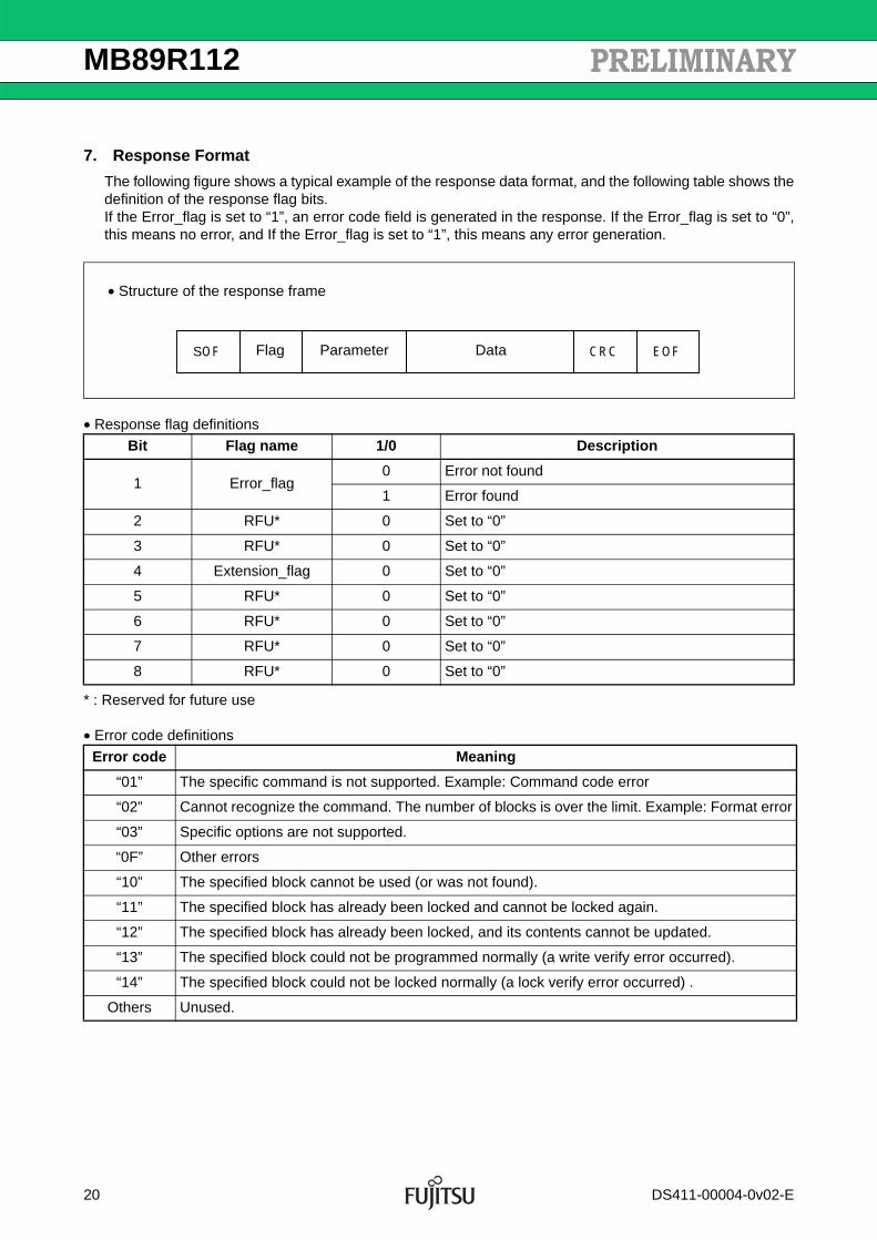
7. Response Format
The following figure shows a typical example of the response data format, and the following table shows thedefinition of the response flag bits.If the Error_flag is set to “1”, an error code field is generated in the response. If the Error_flag is set to “0”,this means no error, and If the Error_flag is set to “1”, this means any error generation.
• Response flag definitions
* : Reserved for future use
• Error code definitions
Bit Flag name 1/0 Description
1 Error_flag0 Error not found
1 Error found
2 RFU* 0 Set to “0”
3 RFU* 0 Set to “0”
4 Extension_flag 0 Set to “0”
5 RFU* 0 Set to “0”
6 RFU* 0 Set to “0”
7 RFU* 0 Set to “0”
8 RFU* 0 Set to “0”
Error code Meaning
“01” The specific command is not supported. Example: Command code error
“02” Cannot recognize the command. The number of blocks is over the limit. Example: Format error
“03” Specific options are not supported.
“0F” Other errors
“10” The specified block cannot be used (or was not found).
“11” The specified block has already been locked and cannot be locked again.
“12” The specified block has already been locked, and its contents cannot be updated.
“13” The specified block could not be programmed normally (a write verify error occurred).
“14” The specified block could not be locked normally (a lock verify error occurred) .
Others Unused.
SOF CRC EOFFlag Parameter Data
• Structure of the response frame
20 DS411-00004-0v02-E

MB89R112
8. Anti-Collision Algorithm
The MB89R112 executes an anti-collision sequence loop based on an algorithm that complies with ISO/IEC15693-3.
The Anti-collision algorithm is designed to examine the transponders located within reader/writer communi-cation areas on the basis of UID.
The reader/writer issues an Inventory command to transponders, and some transponders return responseswhile other transponders do not respond, according to the algorithm described in “10. Execution of InventoryCommand by a Transponder”.
9. Request Parameter
• Request Parameter Settings
Set the reader/writer as follows before issuing the Inventory command.
• The Nb_slots_flag (bit 6), which is a request flag, is set to the desired value : “0” : 16 slots (for plural transponders)“1” : 1 slot (for single transponder)
• A mask length and a mask value are added after the command code.
• The mask length represents the data length of the mask value in bits.
• The mask value is integer bytes of data, transmitted beginning with the lowest bit. If the mask data is not a multiple of 8 (bits) in length, 0 is padded on the MSB side of the mask value so that the data is in units of bytes.
The following figure shows an example of the mask value with padding. Since the mask length is 12 bits,the mask value is padded with 4 bits on the MSB side so that the mask data is in units of bytes (2 bytes =16 bits in this case).
If the AFI flag in the request flags is set in the format explained in “• Structure of the request frame of 6.Request Format”, an AFI field is added to the format. The command ends with transmission of an EOF signalas described in “1. Communication from Reader/Writer to Transponder”. Thereafter, processing in the firstslot starts immediately. To proceed to the next slot, the reader/writer sends an EOF signal.
• Format of the Command
SOF Flag Command code Optional AFI Mask length Mask value CRC EOF
8 bits 8 bits 8 bits 8 bits 0 to 64 bits 16 bits
MSB
Pad
LSB
0000 0100 1100 1111
Mask value
• Example of the Mask Value with Padding
DS411-00004-0v02-E 21

MB89R112
10. Execution of Inventory Command by a Transponder
A transponder returns a response to the reader/writer when its UID is equal to the value that consists of themask value and the number of slots. The mask value is sent in the Inventory command, and the number ofslots is determined by the number of times the EOF signal is transmitted.
• Algorithm for execution of processing by a transponder
The following figure shows the algorithm for the execution of processing by a transponder when an Inventorycommand is received. The next figure shows the relationship between the UID and the mask value.
Nb_slots_flag=1?
SN_length=0 SN_length=4
YES NO
YES
NO
Slot_Frame=SOF?
Slot_Frame=EOF?YES
Wait (Slot_Frame)
NO
YES
NO
YES
NO
SN = 0
NbS = 1 NbS = 16
SN = SN + 1
SN < NbS-1
NbS : Total number of slots (1 or 16)SN : Current slot numberLSB (value, n) : The “n” least significant bits of value& : Concatenation operatorSlot_Frame : SOF or EOF
LSB (UID, SN_length + mask length) = LSB (SN, SN_length) & LSB (mask,
mask length) ?
• Algorithm for Execution of Processing by a Transponder when Inventory Command
Response transmission
End of processing
End of processing
End of processing
22 DS411-00004-0v02-E

MB89R112
LSBMSB
Inventory command includes the mask value and mask length.The mask value is padded with “0” into the higher bit side so to make the byte-unit length (a multiple of 8 bits).
[Inventory command (the side of a reader/writer)]
Padding
000•••Mask value
(specified by the Inventory command)
Mask lengthSlot
counter
Number of slots Mask value (no padding)
Ignored Compared
Unique Identifier (UID)
[Unique Identifier (the side of a transponder) ]
If Inventory command is received, the slot counter is reset to “0”.
If EOF is received, the increment of the slot counter is started by the transponder.
The value is compared with the lowest bit in UID of the transponder.If the value is in accord with the mask value, the response is returned by the transponder.
• Comparison of the mask value and the number of slots with the UID
DS411-00004-0v02-E 23

MB89R112
11. Anti-Collision Sequence
• Execution of anti-collision sequence
The following steps summarize the main cases that can occur during a typical anti-collision sequence wherethe number of slots is 16.
1) The reader/writer sends an Inventory command. The Nb_slots_flag bit of the request flags is set to “0” to specify the number of slots.
2) In slot 0, transponder 1 transmits its response in the time t1_a from the detection of the rising edge of the EOF. In this case no collision occurs and the UID of transponder is received and registered by the reader/writer.
3) The reader/writer sends an EOF signal to switch to the next slot in the time t2_a after the response 1.
4) In slot 1, transponder 2 and transponder 3 transmit their response in the time t1_a from the detection of the rising edge of the EOF. In this case, the reader/writer cannot recognize the UIDs of the two transponders because the collision occurs, and the reader/writer remembers that a collision was detected in slot 1.
5) The reader/writer sends an EOF signal to switch to the next slot in the time t2_a after the responses.
6) In slot 2, no transponder transmits a response. The reader/writer does not detect any response, and sends an EOF signal to switch to the next slot in the time t3_a from the detection of the rising edge of the EOF.
7) In slot 3, transponder 4 and transponder 5 transmit their response in the time t1_a from the detection of the rising edge of the EOF, and another collision occurs.
8) The reader/writer sends a request (for example, a Read Single Block command, described later) to the transponder 1, which UID was already correctly received.
9) All transponders detect an SOF signal and exit the Anti-collision sequence. In this case, since the request is addressed to transponder 1 (Addressed mode), only transponder 1 transmits its response.
10) All transponders are ready to receive another request from the reader/writer. If the Inventory command is sent again, the Anti-collision sequence starts from slot 0.
Note : t1_a, t2_a, t3_a are specified in “12. Timing definitions”.
24 DS411-00004-0v02-E

MB89R112
Slot 0 Slot 1
(2)
(3)
(4)EOF
Response 1
Inventory command
No collision Collision
No response Collision
Response 2
Response 3
EOFSOF
t1_a t2_a t1_a t2_a
(1)
Slot 3Slot 2
(7)
(6)
EOF
Response 4
t1_a t2_at3_a
(5)
EOF EOF
Response 5
(9)
(8)
t1_at3_a
EOFSOF
Slot_Counter
Reader/writer
Reader/writer
Reader/writer
MB89R112
Slot_Counter
MB89R112
Slot_Counter
MB89R112
Status
Status
Status
Timing
Timing
Timing
Command (to Transponder1)
Response (Transponder1)
• Example of Anti-Collision Sequence
DS411-00004-0v02-E 25

MB89R112
12. Timing definitions
(1) Period during which the MB89R112 waits for the start of response transmission after an EOF signaltransmitted from the reader/writer : t1_a
After detection of an EOF signal sent from the reader/writer, MB89R112 must wait for a certain time (t1_a)before sending a response to the reader/writer. t1_a begins at the rising edge of the EOF pulse, and it isdefined as follows. The minimum value is 4320/fc (318.6 μs), the nominal value is 4352/fc (320.9 μs), andthe maximum value is 4384/fc (323.3 μs).
Even if the 10% ASK modulated signal from the reader/writer is detected within the time t1_a, the transponderignore the signal and wait for further time t1_a before starting to transmit.
(2) Period during which the MB89R112 ignores modulated signals after an EOF signal transmittedfrom the reader/writer : tmit
After detection of an EOF signal sent from the reader/writer, MB89R112 must ignore the 10% ASK modulatedsignals from the reader/writer for a time (tmit).tmit begins at the rising edge of the EOF pulse. The minimum value of tmit is defined as 4384/fc (323.3 μs)+ tnrt.In the above expression, tnrt stands for the response time of MB89R112.
(3) Period during which the reader/writer waits before sending a request : t2_a
When the reader/writer has received a response from the transponder to a previous request other thanInventory and Stay Quiet command, it shall wait a time t2_a before sending a subsequent request. Theminimum value of t2_a is 309.2 μs. It is defined in ISO/IEC 15693-3. And ISO/IEC 18000-3 (Mode 1) .
(4) Period during which the reader/writer waits before sending a request during execution of the In-ventory command : t2inv
While an Inventory command is being executed, the reader/writer sends an EOF signal when it shifts to thenext slot. In this case, the wait time is defined as follows depending on whether transponders return responses :
- Wait time applied when the reader/writer has received one or more responses : t2invwrIt is defined in ISO/IEC 15693-3. And ISO/IEC 18000-3 (Mode 1) that when the reader/writer has receivedone or more responses, the reader/writer must wait until responses from the transponders have beencompleted (that is, the reader/writer receives an EOF signal or tnrt passes). After that, the reader/writermust wait until t2_a passes before sending an EOF signal to switch to the next slot.
- Wait time applied when the reader/writer has not received any responses : t3_aWhen the reader/writer has not received any responses from the MB89R112, the reader/writer must waituntil t3_a passes before sending an EOF signal. In this case, t3_a begins at the rising edge of the EOFpulse that was sent previously. The minimum value of t3_a is defined as shown in the following table.
MB89R112 does not support the minimum value of t3_a as “4384/fc (323.3 μs) + tsof” when the reader/writer sends a 100% modulated EOF, which is defined in ISO/IEC 15693-3 and ISO/IEC 18000-3 (Mode 1).
(a) If the reader/writer sends a ASK10% modulated EOF, the minimum value of t3_a (ASK10%) is “4384/fc (323.3 μs + tnrt')
(b) If the reader/writer sends a ASK100% modulated EOF, the minimum value of t3_a (ASK100%) is“4384/fc (323.3 μs + tsof')
tnrt: The nominal response time of transponder
tsof: The time for transponder to transmit a SOF to the reader/writer
26 DS411-00004-0v02-E

MB89R112
• Timing specification
Min Typ Max
t1_a 4320/fc (318.6 μs) 4352/fc (320.9 μs) 4384/fc (323.3 μs)
tmit 4384/fc (323.3 μs) + tnrt ⎯ ⎯
t2_a 4192/fc (309.2 μs) ⎯ ⎯
t2invwr t2_a + tnrt ⎯ ⎯
t3_a (ASK10%) 4384/fc (323.3 μs) + tnrt ⎯ ⎯
t3_a (ASK100%) 4384/fc (323.3 μs) + tsof ⎯ ⎯
tnrt ⎯FastFast
Low data rateHigh data rateLow data rateHigh data rate
::::
15708.163927.047854.081963.52
msmsmsms
⎯
tsof ⎯FastFast
Low data rateHigh data rateLow data rateHigh data rate
::::
604.16151.04302.08
75.52
msmsmsms
⎯
No response
New command (or EOF signal)EOF
Inventory command
Reader/Writer
MB89R112
Timing
MB89R112 ASK signal handling
SOF
t1_a
tsof
tnrt
t3_a (ASK100 %)
t3_a (ASK10 %)
Reset t1_a after receiving
ASK 100 % signal
IgnoreASK 100 %
signal
Ignore ASK 10 % signal
Possible to receive ASK 100 % signal
Possible to receive ASK 10 % signal
• t3_a for ASK10% and ASK100% signal
DS411-00004-0v02-E 27

MB89R112
■ COMMANDS OF RF COMMUNICATION MODEThe following Mandatory and Optional commands defined by ISO/IEC 15693-3 are supported. (partly notsupported: Please refer to ■USAGE NOTES for details).
The following Custom commands are supported : • Fast command : Respond at double speed compared to ISO commands
• Command listCommand
code Command name Command Type Details
“01H” Inventory Mandatory Execute the Anti-collision sequence and get UID.
“02H” Stay Quiet Mandatory Enter the Quiet state.
“20H” Read Single Block OptionalRead the requested 1 block data in the user area/system area.
“21H” Write Single Block Optional Write the requested 1 block data in the user area.
“22H” Lock Block OptionalLock (disable to write) the requested 1 block in the user ar-ea.
“23H” Read Multiple Blocks OptionalRead the requested successive blocks data in the user area/system area (Up to 256 blocks).
“25H” Select Optional Enter the select (communication selected) state.
“26H” Reset to Ready Optional Enter the ready (communication enabled) state.
“27H” Write AFI Optional Write AFI (Application Family Identifier) data.
“28H” Lock AFI Optional Lock AFI data (disable to write).
“29H” Write DSFID Optional Write DSFID (Data Storage Format Identifier) data.
“2AH” Lock DSFID OptionalLock DSFID (Data Storage Format Identifier) data (disable to write).
“2BH” Get System Information OptionalRead the system information value (UID, DSFID, AFI, number of bytes per block, number of blocks in user area, and IC information).
“2CH”Get Multiple Block
Security StatusOptional Read the block security status stored in system area.
“B1H” Fast Inventory Custom Fast response Inventory command.
“BCH” Refresh System Blocks CustomWrite “00H” into the requested block in the user area/system area.
“C0H” Fast Read Single Block Custom Fast response Read Single Block command.
“C1H” Fast Write Single Block Custom Fast response Write Single Block command.
“C3H” Fast Read Multiple Blocks Custom Fast response Read Multiple Blocks command.
“D9H” Read Lock Block CustomLock (disable to write) the requested 1block in the user area.
“DAH”Get Multiple Read Lock
statusCustom Read the read Lock status stored in the system area.
28 DS411-00004-0v02-E

MB89R112
1. Description of Mandatory Commands
1-1. Inventory command
The Inventory command executes the anti-collision sequence. If an error is detected during execution of this command, a response indicating the error shall not be returned.
The Inventory_flag (bit 3) must be set to “1”. When the AFI_flag (bit 5) in the Inventory command frame is set as “1”, the response shall be returned inthe following cases.
• The AFI value of the transponder is in accord with the optional AFI value.• The 4 bits value MSB of the Optional AFI is “0H”, and the 4 bits value LSB of the Optional AFI is in
accord with the 4 bits value LSB of the transponder.• The 4 bits value LSB of the Optional AFI is “0H”, and the 4 bits value MSB of the Optional AFI is in
accord with the 4 bits value MSB of the transponder.• The optional AFI value is “00H”.
• Request
[Request from the reader/writer to the transponder]
• Response
[Response from the transponder to the reader/writer]
1-2. Stay Quiet command
On receiving the Stay Quiet command, the transponder enters the quiet state. The transponder does notreturn any responses, including an error indication.
In the quiet state, the transponder does not execute any request for which the Inventory_flag (bit 3) is set to“1” and executes only a command for which the Address_flag (bit 6) is set to “1”.The transponder exits the quiet state only in the following cases:
• The transponder enters the power-off state.• The transponder receives the Select command and enters the select state.• The transponder receives the Reset to Ready command and enters the ready state.
• Request
[Request from the reader/writer to the transponder]
• Response
[Response from the transponder to the reader/writer]
No response
SOF Flag Command (Inventory) Optional AFI Mask length Mask value CRC EOF
8 bits 8 bits (“01H”) 8 bits 8 bits 0 to 64 bits 16 bits
SOF Flag DSFID UID CRC EOF
8 bits (“00H”) 8 bits 64 bits 16 bits
SOF Flag Command(Stay Quiet) UID (necessary) CRC EOF
8 bits 8 bits (“02H”) 64 bits 16 bits
DS411-00004-0v02-E 29

MB89R112
2. Description of Optional Commands
2-1. Read Single Block command
On receiving the Read Single Block command, the transponder reads the data stored in the specified singleblock to the reader/writer.
If the Option_flag (bit 7) is “1”, the transponder adds block security status information in the response. If theOption_flag (bit 7) is “0”, the transponder returns only the data in the specified block to the reader/writer.
• Request
[Request from the reader/writer to the transponder]
• Response
[Response from the transponder to the reader/writer]
(1) When Error_flag set
(2) When Error_flag not set
2-2. Write Single Block command
On receiving the Write Single Block command, the transponder writes the single block data included in therequest to the specified block.
The transponder performs verification after writing and returns an error code if the writing has failed.If the Option_flag (bit 7) is “0”, the transponder shall return its response when it has completed the writeoperation starting after “t1nom (320.9 μs) + a multiple of 4096/fc (302.1 μs)” with total tolerance of ± 32/fc(2.4 μs) and latest within 20 ms. If it is “1”, transponder shall wait for the reception of an EOF from the reader/writer and upon such reception still return its response (However, if an EOF is not sent within 38 ms, thetime-out occurs and the transponder can receive another command).
• Request
[Request from the reader/writer to the transponder]
SOF Flag Command(Read Single Block)
UID (Addressed mode)
Number of blocks CRC EOF
8 bits 8 bits (“20H”) 64 bits 8 bits 16 bits
SOF Flag Error code CRC EOF
8 bits (“01H”) 8 bits 16 bits
SOF Flag Block security status (option) Data CRC EOF
8 bits (“00H”) 8 bits 256 bits 16 bits
SOF Flag Command(Write Single Block)
UID (Addressed mode)
Number of blocks Data CRC EOF
8 bits 8 bits (“21H”) 64 bits 8 bits 256 bits 16 bits
30 DS411-00004-0v02-E

MB89R112
• Response
[Response from the transponder to the reader/writer]
(1) When Error_flag set
(2) When Error_flag not set
2-3. Lock Block command
On receiving the Lock Block command, the transponder locks (write disable) permanently the data storedin one specified single block.
The transponder performs verification after writing and returns an error code if the writing has failed.
If the Option_flag (bit 7) is “0”, the transponder shall return its response when it has completed the lockoperation starting after “t1nom (320.9 μs) + a multiple of 4096/fc (302.1 μs)” with total tolerance of ± 32/fc(2.4 μs) and latest within 20 ms. If it is “1”, transponder shall wait for the reception of an EOF from the reader/writer and upon such reception still return its response. (However, if an EOF is not sent within 38 ms, thetime-out occurs and the transponder can receive another command.)
Once the Lock Block command has been received, data in the locked block cannot be changed by anycommand.
• Request
[Request from the reader/writer to the transponder]
• Response
[Response from the transponder to the reader/writer]
(1) When Error_flag set
(2) When Error_flag not set
SOF Flag Error code CRC EOF
8 bits (“01H”) 8 bits 16 bits
SOF Flag CRC EOF
8 bits (“00H”) 16 bits
SOF Flag Command(Lock Block)
UID (Addressed mode)
Number of blocks CRC EOF
8 bits 8 bits (“22H”) 64 bits 8 bits 16 bits
SOF Flag Error code CRC EOF
8 bits (“01H”) 8 bits 16 bits
SOF Flag CRC EOF
8 bits (“00H”) 16 bits
DS411-00004-0v02-E 31

MB89R112
2-4. Read Multiple Blocks Command
On receiving the Read Multiple Blocks command, the transponder reads the data stored in the specifiedsuccessive blocks to the reader/writer.
If the Option_flag (bit 7) is “1”, the transponder adds block security status information in the response. If theOption_flag (bit 7) is “0”, the transponder returns only the data in the specified blocks to the reader/writer. The value of the “number of blocks” field specified in the request is the expected number of blocks minus 1.Setting the number of blocks to “01H” makes a request to read 2 blocks. Setting the number of blocks to “00H”makes a request to read 1 block (the request having the same effect as the Read Single Block command).
• Request
[Request from the reader/writer to the transponder]
• Response
[Response from the transponder to the reader/writer]
(1) When Error_flag set
(2) When Error_flag not set
SOF Flag Command(Read Multiple Blocks)
UID (Addressed mode)
First block number
Number of blocks CRC EOF
8 bits 8 bits (“23H”) 64 bits 8 bits 8 bits 16 bits
SOF Flag Error code CRC EOF
8 bits (“01H”) 8 bits 16 bits
SOF Flag Block security status (option) Data CRC EOF
8 bits (“00H”) 8 bits 256 bits 16 bits
Repeated as required
32 DS411-00004-0v02-E

MB89R112
2-5. Select command
Of the transponders that received the Select command, only the transponder whose UID matches the UIDincluded in the request enters the select state and returns a response.
The other transponders, whose UIDs do not match the UID in the request, enter the ready state withoutreturning any response. The Select command is used only in Addressed mode.
• Request
[Request from the reader/writer to the transponder]
• Response
[Response from the transponder to the reader/writer]
(1) When Error_flag set
(2) When Error_flag not set
2-6. Reset to Ready command
On receiving the Reset to Ready command, the transponder enters the ready state.
• Request
[Request from the reader/writer to the transponder]
• Response
[Response from the transponder to the reader/writer]
(1) When Error_flag set
(2) When Error_flag not set
SOF Flag Command (Select) UID (necessary) CRC EOF
8 bits 8 bits (“25H”) 64 bits 16 bits
SOF Flag Error code CRC EOF
8 bits (“01H”) 8 bits 16 bits
SOF Flag CRC EOF
8 bits (“00H”) 16 bits
SOF Flag Command (Reset to Ready) UID (Addressed mode) CRC EOF
8 bits 8 bits (“26H”) 64 bits 16 bits
SOF Flag Error code CRC EOF
8 bits (“01H”) 8 bits 16 bits
SOF Flag CRC EOF
8 bits (“00H”) 16 bits
DS411-00004-0v02-E 33
MB89R112
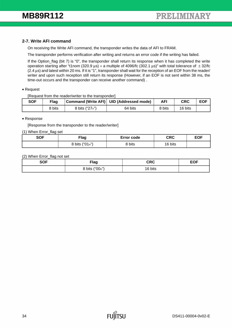
2-7. Write AFI command
On receiving the Write AFI command, the transponder writes the data of AFI to FRAM.
The transponder performs verification after writing and returns an error code if the writing has failed.
If the Option_flag (bit 7) is “0”, the transponder shall return its response when it has completed the writeoperation starting after “t1nom (320.9 μs) + a multiple of 4096/fc (302.1 μs)” with total tolerance of ± 32/fc(2.4 μs) and latest within 20 ms. If it is “1”, transponder shall wait for the reception of an EOF from the reader/writer and upon such reception still return its response (However, if an EOF is not sent within 38 ms, thetime-out occurs and the transponder can receive another command) .
• Request
[Request from the reader/writer to the transponder]
• Response
[Response from the transponder to the reader/writer]
(1) When Error_flag set
(2) When Error_flag not set
SOF Flag Command (Write AFI) UID (Addressed mode) AFI CRC EOF
8 bits 8 bits (“27H”) 64 bits 8 bits 16 bits
SOF Flag Error code CRC EOF
8 bits (“01H”) 8 bits 16 bits
SOF Flag CRC EOF
8 bits (“00H”) 16 bits
34 DS411-00004-0v02-E

MB89R112
2-8. Lock AFI command
On receiving the Lock AFI command, the transponder locks (write disable) permanently the data of AFI.
The transponder performs verification after writing and returns an error code if the writing has failed.
If the Option_flag (bit 7) is “0”, the transponder shall return its response when it has completed the lockoperation starting after “t1nom (320.9 μs) + a multiple of 4096/fc (302.1 μs)” with total tolerance of ±32/fc(2.4 μs) and latest within 20 ms. If it is “1”, transponder shall wait for the reception of an EOF from the reader/writer and upon such reception still return its response (However, if an EOF is not sent within 38 ms, thetime-out occurs and the transponder can receive another command) .
Once the Lock AFI command has been received, the data of AFI cannot be changed by the any command.
• Request
[Request from the reader/writer to the transponder]
• Response
[Response from the transponder to the reader/writer]
(1) When Error_flag set
(2) When Error_flag not set
SOF Flag Command (Lock AFI) UID (Addressed mode) CRC EOF
8 bits 8 bits (“28H”) 64 bits 16 bits
SOF Flag Error code CRC EOF
8 bits (“01H”) 8 bits 16 bits
SOF Flag CRC EOF
8 bits (“00H”) 16 bits
DS411-00004-0v02-E 35

MB89R112
2-9. Write DSFID command
On receiving the Write DSFID command, the transponder writes the data of DSFID to FRAM.
The transponder performs verification after writing and returns an error code if the writing has failed.
If the Option_flag (bit 7) is “0”, the transponder shall return its response when it has completed the writeoperation starting after “t1nom (320.9 μs) + a multiple of 4096/fc (302.1 μs)” with total tolerance of ± 32/fc(2.4 μs) and latest within 20 ms. If it is “1”, transponder shall wait for the reception of an EOF from the reader/writer and upon such reception still return its response (However, if an EOF is not sent within 38 ms, thetime-out occurs and the transponder can receive another command) .
• Request
[Request from the reader/writer to the transponder]
• Response
[Response from the transponder to the reader/writer]
(1) When Error_flag set
(2) When Error_flag not set
SOF Flag Command (Write DSFID) UID (Addressed mode) DSFID CRC EOF
8 bits 8 bits (“29H”) 64 bits 8 bits 16 bits
SOF Flag Error code CRC EOF
8 bits (“01H”) 8 bits 16 bits
SOF Flag CRC EOF
8 bits (“00H”) 16 bits
36 DS411-00004-0v02-E

MB89R112
2-10. Lock DSFID command
On receiving the Lock DSFID command, the transponder locks (write disable) permanently the data of DSFID.
The transponder performs verification after writing and returns an error code if the writing has failed.
If the Option_flag (bit 7) is “0”, the transponder shall return its response when it has completed the lockoperation starting after “t1nom (320.9 μs) + a multiple of 4096/fc (302.1 μs)” with total tolerance of ± 32/fc(2.4 μs) and latest within 20 ms. If it is “1”, transponder shall wait for the reception of an EOF from the reader/writer and upon such reception still return its response (However, if an EOF is not sent within 38 ms, thetime-out occurs and the transponder can receive another command) .
Once the Lock DSFID command has been received, the data of DSFID cannot be changed by any command.
• Request
[Request from the reader/writer to the transponder]
• Response
[Response from the transponder to the reader/writer]
(1) When Error_flag set
(2) When Error_flag not set
SOF Flag Command (Lock DSFID) UID (Addressed mode) CRC EOF
8 bits 8 bits (“2AH”) 64 bits 16 bits
SOF Flag Error code CRC EOF
8 bits (“01H”) 8 bits 16 bits
SOF Flag CRC EOF
8 bits (“00H”) 16 bits
DS411-00004-0v02-E 37

MB89R112
2-11. Get System Information command
On receiving the Get System Information command, the transponder reads the chip information of UID, AFI,DSFID, and so on to the reader/writer as a response.
• Request
[Request from the reader/writer to the transponder]
• Response
[Response from the transponder to the reader/writer]
(1) When Error_flag set
(2) When Error_flag not set
The followings show the definitions of the Information flag and the memory size information (transpondermemory size information) included in the response of the Get System Information command. However, thesize of blocks and number of blocks in the user area shown in the memory size information about a tran-sponder indicate one less than the actual value.
• Definition of information flag
* : Reserved for future use
Note : For MB89R112, set “0FH” (set “1” for bit 1 to bit 4 and set “0” for bit 5 to bit 8) .
SOF Flag Command (Get System Information) UID (Addressed mode) CRC EOF
8 bits 8 bits (“2BH”) 64 bits 16 bits
SOF Flag Error code CRC EOF
8 bits (“01H”) 8 bits 16 bits
SOF Flag Information flag UID DSFID AFI Memory size IC reference CRC EOF
8 bits (“00H”) 8 bits 64 bits 8 bits 8 bits 16 bits 8 bits 16 bits
Bit Flag name State Description
1 DSFID0 DSFID does not exist.
1 DSFID is supported.
2 AFI0 AFI does not exist.
1 AFI is supported.
3 Memory size0 Memory size information does not exist.
1 Memory size information is supported.
4 IC reference0 IC reference information does not exist.
1 IC reference information is supported.
5 RFU* ⎯
Set to “0”6 RFU* ⎯7 RFU* ⎯8 RFU* ⎯
38 DS411-00004-0v02-E

MB89R112
• Memory size information about a transponder
* : Reserved for future use
Note : The memory size of the MB89R112 which consists of 256 blocks (32 bytes per block) in the user area, the memory size information is hexadecimal “1FFFH”.
2-12. Get Multiple Block Security Status Command
On receiving the Get Multiple Block Security Status command, the transponder reads the block securitystatus stored in a system area to the reader/writer as a response.
Up to 256 blocks of data can be read for one request. The number of blocks specified in this request mustbe the value that is 1 block less than the actual number of the blocks whose security status is to be obtained.
The first block number specified in this request must be a multiple of 8.
• Request
[Request from the reader/writer to the transponder]
• Response
[Response from the transponder to the reader/writer]
(1) When Error_flag set
(2) When Error_flag not set
SOF FlagCommand
(Get Multiple Block Security Status)
UID (Addressed mode)
First block number
Number of blocks CRC EOF
8 bits 8 bits (“2CH”) 64 bits 8 bits 8 bits 16 bits
SOF Flag Error code CRC EOF
8 bits (“01H”) 8 bits 16 bits
SOF Flag Block security status CRC EOF
8 bits (“00H”)8 bits
(repeated as required)16 bits
MSB LSB
16 14 13 9 8 1
RFU* Size of blocks (Number of bytes in 1 block)Number of blocks in
the user area
DS411-00004-0v02-E 39

MB89R112
3. Description of Custom Command
The IC manufacturing code is required to use a Custom command. The IC manufacturing code for theMB89R112 is “08H”.
3-1. Fast Inventory Command
The Fast Inventory command is the same as the Inventory Command that executes the anti-collision se-quence.
The data rate in the response is twice as defined in ISO/IEC 15693.
If error is detected during execution of this command, a response indicating the error shall not be returned.
The Inventory_flag (bit 3) must be set to “1”. When the AFI_flag (bit 5) in the Inventory command frame is set as “1”, the response shall be returned inthe following cases.
• The AFI value of the transponder is in accord with the optional AFI value.• The 4 bits value MSB of the Optional AFI is “0H”, and the 4 bits value LSB of the Optional AFI is in
accord with the 4 bits value LSB of the transponder.• The 4 bits value LSB of the Optional AFI is “0H”, and the 4 bits value MSB of the Optional AFI is in
accord with the 4 bits value MSB of the transponder.• The optional AFI value is “00H”.
• Request
[Request from the reader/writer to the transponder]
• Response
[Response from the transponder to the reader/writer]
SOF Flag Command(Fast Inventory)
IC manufacturer code (necessary)
Optional AFI
Mask length
Mask value CRC EOF
8 bits 8 bits (“B1H”) 8 bits (“08H”) 8 bits 8 bits 0 to 64 bits 16 bits
SOF Flag DSFID UID CRC EOF
8 bits (“00H”) 8 bits 64 bits 16 bits
40 DS411-00004-0v02-E

MB89R112
3-2. Refresh System Blocks Command
The Refresh System Blocks command write “00H” into the requested area of FRAM.
When the requested area is in the system area, “00H” shall be written into excepting UID area.
If the requested area is user area , there is no limitation to execute the Refresh System Blocks command.However if the requested area is system area, the Refresh System Blocks command can be executed onlyonce.
If the Option_flag (bit 7) is “0”, the transponder shall return its response when it has completed the lockoperation starting after “t1nom (320.9 μs) + a multiple of 4096/fc (302.1 μs)” with total tolerance of ± 32/fc(2.4 μs) and latest within 20 ms. If it is “1”, the transponder shall wait for the reception of an EOF from thereader/writer, and upon such reception still return its response. (However, if an EOF is not sent within 38ms, the time-out occurs and the transponder can receive another command. )
• Request
[Request from the reader/writer to the transponder]
• Response
[Response from the transponder to the reader/writer]
(1) When Error_flag set
(2) When Error_flag not set
Bank Number The Block for Refresh
00H User area 00H to 3FH
01H User area 40H to 7FH
02H User area 80H to BFH
03H User area C0H to FFH
FFH System area (The UID area is excluded.)
Except the above Prohibition of a setup (A 10H error reply is returned. )
SOF Flag Command (Refresh System Blocks)
IC manufacturer code
UID (Addressed mode)
Bank Number CRC EOF
8 bits 8 bits (“BCH”) 8 bits (“08H”) 64 bits 8 bits 16 bits
SOF Flag Error code CRC EOF
8 bits (“01H”) 8 bits 16 bits
SOF Flag CRC EOF
8 bits (“00H”) 16 bits
DS411-00004-0v02-E 41

MB89R112
3-3. Fast Read Single Block Command
The Fast Read Single Block command is the same as the Read Single Block command that reads the datastored in the specific single block. The data rate in the response is twice as defined in ISO/IEC 15693.
If the Option_flag (bit 7) is “1”, the transponder adds block security status information in the response. If theOption_flag (bit 7) is “0”, the transponder returns only the data in the specified block to the reader/writer.
• Request
[Request from the reader/writer to the transponder]
• Response
[Response from the transponder to the reader/writer]
(1) When Error_flag set
(2) When Error_flag not set
3-4. Fast Write Single Block Command
The Fast Write Single Block command is the same as the Write Single Block command that writes the singleblock data included in the request. The data rate in the response is twice as defined in ISO/IEC 15693.
The transponder performs verification after writing and returns an error code if the writing has failed. If the Option_flag (bit 7) is “0”, the transponder shall return its response when it has completed the writeoperation starting after “t1nom (320.9 μs) + a multiple of 4096/fc (302.1 μs)” with total tolerance of ±32/fc(2.4 μs) and latest within 20 ms. If it is “1”, transponder shall wait for the reception of an EOF from the reader/writer and upon such reception still return its response (However, if an EOF is not sent within 38 ms, thetime-out occurs and the transponder can receive another command) .
• Request
[Request from the reader/writer to the transponder]
• Response
[Response from the transponder to the reader/writer]
(1) When Error_flag set
(2) When Error_flag not set
SOF Flag Command(Fast Read Single Block)
IC manufacturer code (necessary)
UID (Addressed mode)
Block number CRC EOF
8 bits 8 bits (“C0H”) 8 bits (“08H”) 64 bits 8 bits 16 bits
SOF Flag Error code CRC EOF
8 bits (“01H”) 8 bits 16 bits
SOF Flag Block security status(option) Data CRC EOF
8 bits (“00H”) 8 bits 256 bits 16 bits
SOF Flag Command (Fast Write Single Block)
IC manufacturer code (necessary)
UID (Addressed
mode)
Block number Data CRC EOF
8 bits 8 bits (“C1H”) 8 bits (“08H”) 64 bits 8 bits 256 bits 16 bits
SOF Flag Error code CRC EOF
8 bits (“01H”) 8 bits 16 bits
SOF Flag CRC EOF
8 bits (“00H”) 16 bits
42 DS411-00004-0v02-E

MB89R112
3-5. Fast Read Multiple Blocks Command
The Fast Read Multiple Blocks command is the same as the Read Multiple Blocks command that reads thedata of the specified successive blocks.
Up to 256 blocks of data can be read for one request. The data rate in the response is twice as defined inISO/IEC 15693.
If the Option_flag (bit 7) is “1”, the transponder adds block security status information in the response. If theOption_flag (bit 7) is “0”, the transponder returns only the data in the specified blocks to the reader/writer.The value of the “number of blocks” field specified in the request is the expected number of blocks minus 1.Setting the number of blocks to “01H” makes a request to read 2 blocks. Setting the number of blocks to “00H”makes a request to read 1 block (the request having the same effect as the Fast Read Single Block command).
• Request
[Request from the reader/writer to the transponder]
• Response
[Response from the transponder to the reader/writer]
(1) When Error_flag set
(2) When Error_flag not set
SOF FlagCommand(Fast Read
Multiple Blocks)
IC manufacturer code (necessary)
UID (Addressed
mode)
First block
number
Number of
blocksCRC EOF
8 bits 8 bits (“C3H”) 8 bits (“08H”) 64 bits 8 bits 8 bits 16 bits
SOF Flag Error code CRC EOF
8 bits (“01H”) 8 bits 16 bits
SOF Flag Block security status(option) Data CRC EOF
8 bits (“00H”) 8 bits 256 bits 16 bits
Repeated as required
DS411-00004-0v02-E 43

MB89R112
3-6. Read Lock Block Command
On receiving the Read Lock Block command, the transponder locks (read disable) permanently the datastored in one specified single-block. The transponder performs verification after writing and returns an errorcode if the writing has failed.
If the Option_flag (bit 7) is “0”, the transponder shall return its response when it has completed the lockoperation starting after “t1nom (320.9 μs) + a multiple of 4096/fc (302.1μs)” with total tolerance of ± 32/fc(2.4 μs) and latest within 20 ms. If it is “1”,the transponder shall wait for the reception of an EOF from thereader/writer, and upon such reception still return its response (However, if an EOF is not sent within 38 ms,the time-out occurs and the transponder can receive another command).
Once the Read Lock Block command has been received, data in the locked block cannot read by the ReadSingle Block command. On the other hand, if the locked block is accessed as part of the selected blocks bythe Read Multiple Blocks command, the data of the locked block is indicated as “00H” among the batch ofthe data.
• Request
[Request from the reader/writer to the transponder]
• Response
[Response from the transponder to the reader/writer] (1) When Error_flag set
(2) When Error_flag not set
SOF Flag Command (Read Lock Block)
IC manufacturer code
UID (Addressed mode)
Block number CRC EOF
8 bits 8 bits (“D9H”) 8 bits (“08H”) 64 bits 8 bits 16 bits
SOF Flag Error code CRC EOF
8 bits (“01H”) 8 bits 16 bits
SOF Flag CRC EOF
8 bits (“00H”) 16 bits
44 DS411-00004-0v02-E

MB89R112
3-7. Get Multiple Read Lock Status Command
On receiving the Get Multiple Read Lock Status command, the transponder reads the Read Lock status stored in the system area.
Up to 256 blocks of status can be read for one request. The number of blocks specified in this request mustbe the value that is 1 block less than the actual number of whose security status is to be obtained.
The first block number specified in this request must be a multiple of 8.
• Request
[Request from the reader/writer to the transponder]
• Response
[Response from the transponder to the reader/writer](1) When Error_flag set
(2) When Error_flag not set
SOF FlagCommand
(Get Multiple Read Lock Status)
IC manufacturer
code
UID (Ad-
dressed mode)
First block
number
Number of blocks CRC EOF
8 bits 8 bits (“DAH”) 8 bits (“08H”) 64 bits 8 bits 8 bits 16 bits
SOF Flag Error code CRC EOF
8 bits (“01H”) 8 bits 16 bits
SOF Flag Read Lock Status CRC EOF
8 bits8 bits
(repeated as required)16 bits
DS411-00004-0v02-E 45

MB89R112
4. Command Execution Time
4-1. Write Single Block Command Execution Time
The minimum time (processing in the Addressed mode) required to complete data writing to all user areas(8192 bytes) of the FRAM and verification with the Write Single Block command is estimated to be 4.0 seconds.
4-2. Read Multiple Blocks Command Execution Time
The minimum time (processing in the Addressed mode) required to complete data reading for all user areas(8192 bytes) of the FRAM with the Read Multiple Blocks command is estimated to be 2.5 seconds.In addition, with the Fast Read Multiple Blocks command is estimated to be 1.3 seconds.
46 DS411-00004-0v02-E

MB89R112
■ COMMANDS OF SERIAL COMMUNICATION MODEThis LSI accepts 5 commands specified in Op-code is an 8 bits code as shown in the table below.If other codes are inputted, the command is ignored. If XCS is risen during the input sequence of Op-code,the command cannot be executed.
• OP-code of Serial Interface
1. READ
The READ command is executed in units of 16 bits.
Op-code and 16 bits address are input through SI. The upper 3 address bits don't care. Then, the data isread through SO synchronously to the falling edge of SCK.
During the data reading, the SI value is invalid. The reading address is automatically incremented by each16-cycle clock input until XCS is rising. If the most significant address is reached, the counter rolls over to“0000H”. When the start address is specified in the user area. If the start address is specified in the lockinformation of system area (1000H to 103FH), the counter rolls over to “1000H”.
The rising edge of XCS terminate the READ operation.
The READ command can be executed in the User area and Lock status areas. If the specified blocks are inRead Locked, “0000H” is output instead of the data.
[SI input:Controller (external SPI access circuit) → MB89R112]
[SO output:MB89R112 → Controller (external SPI access circuit)](1) In the case of a 1-cycle read
(2) In the case of a continuous cycle read*
*: A continuous cycle read is continued until a stop or XCS of SCK negates (XCS = H).
Name Function OP-code
READ Read from the user area in units of 16 bits. 0000 0011
WRITE Write to the user area in units of 16 bits. 0000 0010
RD_LOCK Set up to the read prohibition area in the user area. 0000 1001
WR_LOCK Set up to the write prohibition area in the user area. 0000 1000
RD_UID Read the UID. 0000 1100
OP-code (READ) Address
8 bits (“03H” ) 16 bits
Data Out
16 bits
Data Out1 Data Out2
16 bits 16 bits ···
0
0 0 0 0 0 0
1
9 4 3 1 02. . .1 1
2 3
X X X 12 11 10
4 5 6 7 8 9 10 11 12 13 18 19 20 21 22 23 24 25 26 27 28 29 30 31 32 33 34 35 36 37 38 39
Invalid
Invalid
Data Out LSBLSB MSB
15 14 13 12 11 10 9 8 7 6 5 4 3 2 1 0
MSB
SO
SI
SCK
XCS
High-Z
16-bit AddressOP-CODE
DS411-00004-0v02-E 47

MB89R112
2. WRITE
The WRITE command is executed in units of 16 bits. Op-code and 16 bits address are input through SI. Theupper 3 address bits don't care. The writing address (“0FFFH”) is automatically incremented by each 16-cycle clock input until XCS is rising. If the most significant address is reached, the counter rolls over to“0000H”. The rising edge of XCS terminate the WRITE operation.
The WRITE command can be executed in the User area. If the specified blocks are in Write Locked, it cannotwrite and writing is disregarded.
[SI input: Controller (external SPI access circuit) → MB89R112](1) In the case of a 1-cycle write
(2) In the case of a continuous cycle write*
* : A continuous cycle write is continued until a stop or XCS of SCK negates (XCS = H).
[SO output:MB89R112 → Controller(external SPI access circuit)]
OP-code (WRITE) Address Data
8 bits (“02H”) 16 bits 16 bits
(WRITE) Address Data1 Data2
8 bits (“02H”) 16 bits 16 bits 16 bits ···
Data Out
Nothing (High-Z)
0
0 0 0 0 0 0
1
9 4 3 1 02. . .1 0
2 3
X X X 12 11 10
4 5 6 7 8 9 10 11 12 13 18 19 20 21 22 23 24 25 26 27 28 29 30 31 32 33 34 35 36 37 38 39
LSBLSB
Data In
MSB
15 14 13 12 11 10 9 8 7 6 5 4 3 2 1 0
MSB
SO
SI
SCK
XCS
High-Z
16-bit AddressOP-CODE
48 DS411-00004-0v02-E

MB89R112
3. RD_LOCK
The RD_LOCK command reads the FRAM memory cell array in blocks to restrict reading access. The OP-code of RD_LOCK, a 1-bit readable/unreadable specifier and a 8-bit block number are input to SI.The block is specified by the upper 8 bits.
[SI input:Controller (external SPI access circuit) → MB89R112]
[SO output: MB89R112 → Controller(external SPI access circuit)]
OP-code (RD_LOCK) Data In
8 bits (“09H”) 16 bits
Data Out
Nothing(High-Z)
Data In Function Remarks
Bit15 to Bit8 Specify the block number 00H to FFH (USER area)
Bit7 1: Read is impossible 0: Read is possible
Bit6 to Bit0 Unused (Don't Care)
0 1 2 3 4 5 6 7 8 9 10 11 12 13 14 15 16 17 18 19 20 21 22 23
SO
SI
SCK
XCS
High-Z
Data InOP-CODE
0 0 0 0 1 0 9 8 X X70 1 15 14 13 12 11 10 X X X X X
DS411-00004-0v02-E 49

MB89R112
4. WR_LOCK
The WR_LOCK command restricts writing access to the FRAM memory cell array in blocks. The OP-code of WR_LOCK, a 1-bit readable/unreadable specifier and a 8-bit block number are input to SI.The block is specified by the upper 8 bits.
[SI input: Controller (external SPI access circuit) → MB89R112]
[SO output:MB89R112 → Controller(external SPI access circuit)]
OP-code (WR_LOCK) Data In
8 bits (“08H”)
16 bits
Data Out
Nothing (High-Z)
Data In Function Remarks
Bit15 to Bit8 Specify the block number 00H to FFH (USER area)
Bit7 1: Write is impossible 0: Write is possible
Bit6 to Bit0 Unused (Don't Care)
0
0 0 0 0 1 0
1
9 8 X X70 0
2 3
15 14 13 12 11 10
4 5 6 7 8 9 10 11 12 13 14 15 16 17 18 19 20 21 22 23
X X X X
SO
SI
SCK
XCS
High-Z
X
Data InOP-CODE
50 DS411-00004-0v02-E

MB89R112
5. RD_UID
The RD_UID command reads UID (64 bits). After the OP-code of RD_UID is input to SI, a 64-cycle clock is input to SCK. In this case, the SI value isinvalid. SO is output synchronously to the falling edge of SCK. When, in the RD_UID command, UID (64 bits) is output, and then SCK continues to be sent before thestartup of XCS, SO maintains the output status of the last bit.
[SI input:Controller (external SPI access circuit) → MB89R112]
[SO output:MB89R112 → Controller (external SPI access circuit)]
OP-code (RD_UID)
8 bits (“0CH”)
Data Out
UID (64bit)
Data Out Function Remarks
Bit63 to Bit0 UID outputRefer to “■ DATA ELEMENT DEFINITION
1. Unique Identifier (UID)” for details.
0
0 0 0 0 1
1
. . .
. . .
1
2 3
0 0
4 5 6 7 8 9 10 11 12 13 14 63 64 65 66 67 68 69 70 71
Data Out (64bit)
Invalid
LSB
63 62 61 60 59 58 57 56 7 6 5 4 3 2 1 0
MSB
SO
SI
SCK
XCS
High-Z
OP-CODE
DS411-00004-0v02-E 51

MB89R112
■ STATE TRANSITION DIAGRAM• Definition of states for RF communication
Each state of MB89R112 is defined as follows.
• Power-off state : In the power-off state, a transponder cannot fulfill the function so that the voltage from a reader/writer is underpowered.
• Ready state : In the ready state, the MB89R112 can execute all commands if the Select_flag is not set.
• Quiet state : In the quiet state, the MB89R112 can execute the command for which the Inventory_flag is not set and the Address_flag is set.
• Select state : In the select state, the MB89R112 can execute the command for which the Select_flag is set.
As shown in figure below, the MB89R112 moves from one state to another according to the status of powerand by a command.
Power-off state Out of fieldOut of field
Out of field In field
Any other command where Select_flag = 1 is not set.
Ready state
Select command (UID) Reset to Ready command or Select command (different UID) .
Reset to Ready command
Stay Quiet command (UID)
Quiet state Select state
Stay Quiet command (UID)
Select command (UID)
Any other commandAny other commandwhere Address_flag = 1 is set and where Inventory_flag is not set.
• State transition diagram
52 DS411-00004-0v02-E

MB89R112
■ ABSOLUTE MAXIMUM RATINGS
WARNING: Semiconductor devices can be permanently damaged by application of stress (voltage, current, temperature, etc.) in excess of absolute maximum ratings. Do not exceed these ratings.
Parameter SymbolRating
Unit RemarksMin Max
Maximum input voltage Imax ⎯ 90 mAP-P Between PWRP-PWRM
Power supply voltage VDD ⎯ 4 V
Input voltage IRF ⎯ 30 mArms Antenna connected.
ESD voltage immunity |VESD|⎯ 2 kV Human Body Model
⎯ 200 V Machine Model
Storage temperature Tstg − 55 + 125 °C Excluding FRAM data retention guarantee
DS411-00004-0v02-E 53

MB89R112
■ RECOMMENDED OPERATING CONDITIONS
WARNING: The recommended operating conditions are required in order to ensure the normal operation of the semiconductor device. All of the device's electrical characteristics are warranted when the device is operated within these ranges.
Always use semiconductor devices within their recommended operating condition ranges. Operation outside these ranges may adversely affect reliability and could result in device failure.No warranty is made with respect to uses, operating conditions, or combinations not represented on the data sheet. Users considering application outside the listed conditions are advised to contact their representatives beforehand.
Note: However, because the communication characteristics is deeply related with the combination of antenna, reader/writer, and operating environment, this condition does not ensure the complete operation of transponders. Therefore it is recommended to confirm the communication characteristics with the actual antenna and reader/writer beforehand.
The values are confirmed with a reference antenna in the input capacitance 23 pF products, and its parameters are as follows.
External size : 75 mm × 46 mmNumber of turns : 6Width of conductor : 1 mmSpace between 2 conductors : 0.4 mm
Parameter SymbolValue
Unit RemarksMin Typ Max
Minimum antenna input voltage VRF ⎯ 7.5 10.2 VP-P Antenna connected.
ASK modulation index (10%) m 10 ⎯ 30 %
ASK modulation index (100%) m 95 ⎯ 100 %
ASK pulse width (10%)
t1 6.00 ⎯ 9.44 μs
t2 3.0 ⎯ t1 μs
t3 0 ⎯ 4.5 μs
ASK pulse width (100%)
t1 6.00 ⎯ 9.44 μs
t2 2.1 ⎯ t1 μs
t3 0 ⎯ 4.5 μs
t4 0 ⎯ 0.8 μs
Input frequency Fin 13.553 13.560 13.567 MHz
Operating temperature Ta − 20 ⎯ + 85 °C
Operating voltage VDD 3.0 3.3 3.6 V Serial communication
“H” level input voltage
SPI
VIH
VDD − 0.3 ⎯ VDD + 0.3 V
XCS, SCK, SI
VDD × 0.8 ⎯ VDD + 0.3 V
“L” level input voltage VIL − 0.3 ⎯ + 0.6 V
54 DS411-00004-0v02-E

MB89R112
■ ELECTRICAL CHARACTERISTICS
1. RF Communication
* : The capacitance value is an alternative value, which is distinguished with the part number. The values are controlled by PCM (Process Control Monitor) in the wafer.
2. Serial Communication
• DC Characteristics
Parameter SymbolValue
Unit RemarksMin Typ Max
Load modulation resistance RlSW ⎯ 1.1 ⎯ kΩ
Input capacitance*23pF
Cant21.85 23.00 24.15
pFVoltage between antennas = 2 Vrms96pF 86.4 96.0 105.6
Parameter Sym-bol
ValueUnit Remarks
Min Typ Max
Input leakage current ILI 0 ⎯ 5 μA VIN = 0 V to VDD
Output leakage current ILO 0 ⎯ 5 μAVOUT = 0 V to VDD, when output pin is Hi-Z
Power supply
Operating current ICC ⎯ 97200
(TBD)μA SCK = 2 MHz
Power down current 1 IPD1 ⎯ 0.01 5 (TBD) μASPI = 0 V or open XCS, SCK, SI = 0 V or VDD No RF reception
Power down current 2 IPD2 ⎯ 7 15 (TBD) μASPI = 0 V or openXCS, SCK, SI = 0 V or VDD RF receiving
Standby current ISB ⎯ 25 50 (TBD) μASPI = VDD
XCS, SCK, SI = 0 V or VDD
“H” level output voltage VOH VDD × 0.8 ⎯ VDD V IOH = − 1 mA
“L” level output voltage VOL 0 ⎯ 0.4 V IOL = 2 mA
SPI pin pull-down resistance RIN 0.8 1 1.2 MΩ VIN = VDD
DS411-00004-0v02-E 55

MB89R112
• AC Characteristics
Parameter SymbolValue
UnitMin Max
SCK clock frequency fCK ⎯ 2 MHz
Clock high time tCH 200 ⎯ ns
Clock low time tCL 30 ⎯ ns
Chip select set time tCSU 10 ⎯ ns
Chip select hold time tCSH 10 ⎯ ns
Output disable time tOD ⎯ 20 ns
Output data valid time tODV ⎯ 35 ns
Output hold time tOH 0 ⎯ ns
Deselect time tD 200 ⎯ ns
Data rise time tR ⎯ 50 ns
Data fall time tF ⎯ 50 ns
Data set up time tSU 10 ⎯ ns
Data hold time tH 10 ⎯ ns
High-Z High-Z
XCS
SCK
SI Valid in
tSU
tCH tCL
tCSH
tD
tODtOHtODV
tH
SO
: don’t care
tCSU
tFtR
• Serial data timing
56 DS411-00004-0v02-E

MB89R112
■ USAGE NOTES• Notes on the RF interface
- The performance of transponder is determined by not only LSI specification but also antenna design and reader/writer characteristics. Therefor it is recommended for the customers to optimize the antenna and reader/writer according to the required communication distance and usage environment.
- If the user intends to access multiple transponders from a reader/writer, the interference between transponders or between the reader/writer and a transponder may degrade communication performance (transmission distance and communication time) . Therefore, a user who intends to design a system using multiple transponders should consider this point.
• FRAM Characteristics
*1 : Total number of reading and writing defines the minimum value of endurance, as an FRAM memory operates with destructive readout mechanism.
*2 : Minimun values define retention time of the first reading/writing data right after shipment.
*3 : This value is calculated by reliability test results for reference as well.
• Differences of the function between ISO/IEC15693 and MB89R112.
The comparison of the function between ISO/IEC 15693 and MB89R112 is shown in the table below. MB89R112 does not support the following functions.• 1 out of 256 data coding• 2-subcarrier • Write Multiple Blocks command
ItemValue
Unit ParameterMin Max
Read/Write Endurance*1 ⎯ Times/byte Operation Ambient Temperature TA = + 85 °C
Data Retention*210 ⎯
YearsOperation Ambient Temperature TA = + 85 °C
30 ⎯ Operation Ambient Temperature TA = + 70 °C*3
DS411-00004-0v02-E 57

MB89R112
• MB89R112 functions compared with ISO/IEC15693Parameter ISO/IEC15693 specification MB89R112
Modulation10% ASK Support
100% ASK Support
Data coding1 out of 256 Not support
1 out of 4 Support
Subcarrier1-subcarrier Support
2-subcarrier Not support
Mandatory commandInventory command Support
Stay Quiet command Support
Optional command
Read Single Block command Support
Write Single Block command Support
Lock Block command Support
Read Multiple Blocks command Support
Write Multiple Blocks command Not support
Select command Support
Reset to Ready command Support
Write AFI command Support
Lock AFI command Support
Write DSFID command Support
Lock DSFID command Support
Get System Information command Support
Get Multiple Block Security Status command Support
58 DS411-00004-0v02-E

MB89R112
■ RECOMMENDED ASSEMBLY CONDITIONS (WAFER)The MB89R112 is recommended to be mounted in the following condition to maintain the data retentioncharacteristics of the FRAM memory when the chip is mounted.
- Mounting temperature of + 175 °C or lower, and 120 minutes or shorter when applied at high temperature, or- Mounting temperature of + 200 °C or lower, and 60 seconds or shorter when applied at high temperature
+175
+25
120
+200
+25
60
Tem
pera
ture
[ °C
]
Time [min]
Tem
pera
ture
[ °C
]
Time [s]
DS411-00004-0v02-E 59

MB89R112
■ REFLOW CONDITIONS AND FLOOR LIFE (PACKAGE) [ JEDEC MSL ] : Moisture Sensitivity Level 3 (IPC/JEDEC J-STD-020D)
Data written before reflow cannot be guaranteed. We recommend that Refresh System Blocks commandbe executed to initialize all FRAM memory areas after reflow.
60 DS411-00004-0v02-E

MB89R112
■ ORDERING INFOMATION
* : IC orientation
Part number Input capacitance Shipping method Marking of Failed Chips
MB89R112A1-DIAP15-JN 23pFWafer (After dicing) with Frame
Au Plating Bump Wafer thickness: 150 μm ± 25.4 μm
Wafer map
MB89R112A1-DIAP15-JNP1 23pF Bad mark
MB89R112A2-DIAP15-JN 96pF Wafer map
MB89R112A2-DIAP15-JNP1 96pF Bad mark
Part number Input capacitance Shipping method IC orientation
MB89R112B1QN-G-AMEFE1 23pF24-pin plastic QFN
(LCC-24P-M64) Tape & Reel
EF type*MB89R112B2QN-G-AMEFE1 96pF
MB89R112B1QN-G-AMERE1 23pF ER type*
MB89R112B2QN-G-AMERE1 96pF
(User Direction of Feed)
(User Direction of Feed)
(User Direction of Feed)(Reel side)
• EF type
• ER type Index mark
Index mark
(Reel side)
DS411-00004-0v02-E 61

MB89R112
■ PACKAGE DIMENSION
Please check the latest package dimension at the following URL.http://edevice.fujitsu.com/package/en-search/
Note : To secure the floating area under the center pad of a package at mounting on the printed board, do not attach a ground part on the board.
24-pin plastic QFN Lead pitch 0.50 mm
Package width ×package length
4.0 mm × 4.0 mm
Sealing method Plastic mold
Mounting height 0.75 mm MAX
Weight 0.035 g
24-pin plastic QFN(LCC-24P-M64)
(LCC-24P-M64)
C 2010 FUJITSU SEMICONDUCTOR LIMITED HMbc24-64Sc-1-1
INDEX AREA
(.157±.003)4.00±0.07
4.00±0.07(.157±.003)
2.60±0.10
0.50(.020)TYP (.016±.003)
0.40±0.07
1PIN CORNER(C0.30(C.012))
0.22±0.05(.009±.002)
(.028±.002)0.70±0.05
(0.15(.006))
(.102±.004)
2.60±0.10(.102±.004)
(0.05(.002)) MAX
Dimensions in mm (inches).Note: The values in parentheses are reference values.
62 DS411-00004-0v02-E

MB89R112
■ MAJOR CHANGES IN THIS EDITIONA change on a page is indicated by a vertical line drawn on the left side of that page.
Page Section Change Results
1
■ DESCRIPTION Revised the description.
■ FEATURES Revised the Data retention.10 years ( + 85 °C) → 10 years ( + 85 °C), 30 years ( + 70 °C)
2 ■ PIN ASSIGNMENT Revised the table.
7
■ SERIAL INTERFACE6. XCS Level Hold Time at Power ON/OFF
Added the following description:“If VDD falls down below 2.0 V, VDD is required to be started from 0 V to prevent malfunctions when the power is turned on again.”
Deleted the following description:“Note: Since power ON from middle-level may cause malfunction, VDD should rise from 0 V at power ON.”
Added the following description :“If the device does not operate within the specified conditions of read cycle, write cycle or power on/off sequence, memory data can not be guaranteed.”
8■ MEMORY1. Memory Map• FRAM memory configuration
Revised the table and moved the “Lock Area” under the this table. Revised the table of “Lock Area”.
32■ COMMAND OF RF COMMUNICATION MODE2-4. Read Multiple Blocks Command
Deleted the Note.
392-12. Get Multiple Block Security Status Command
Revised the following description:“64 blocks” → “256 blocks”
43 3-5. Fast Read Multiple Blocks Command Deleted the Note.
453-7. Get Multiple Read Lock Status Com-mand
Added the following description: “Up to 256 blocks of status can be read for one request.”
54■ RECOMMENDED OPERATING CON-DITIONS
Revised the value of “Minimum antenna input voltage”. (Typ) 6.2, (Max) 6.5 → (Typ) 7.5, (Max) 10.2
57■ USAGE NOTES• FRAM Characteristics
Revised the description.
59
■ RECOMMENDED ASSEMBLY CONDI-TIONS (WAFER)
Deleted the following description:“FUJITSU SEMICONDUCTOR does not guarantee that the data written in FRAM before assembly is still retained after assembly. After assembly, the user will have to clear the data in the system area specified by Refresh System Blocks Command.”
60
■ REFLOW CONDITIONS AND FLOOR LIFE (PACKAGE)
Revised the condition to JEDEC compliant.
Added the following description:“Data written before reflow cannot be guaranteed. We recommend that Refresh System Blocks command be executed to initialize all FRAM memory areas after re-flow.”
DS411-00004-0v02-E 63

MB89R112
FUJITSU SEMICONDUCTOR LIMITEDNomura Fudosan Shin-yokohama Bldg. 10-23, Shin-yokohama 2-Chome,Kohoku-ku Yokohama Kanagawa 222-0033, JapanTel: +81-45-415-5858http://jp.fujitsu.com/fsl/en/
For further information please contact:
North and South AmericaFUJITSU SEMICONDUCTOR AMERICA, INC.1250 E. Arques Avenue, M/S 333Sunnyvale, CA 94085-5401, U.S.A.Tel: +1-408-737-5600 Fax: +1-408-737-5999http://us.fujitsu.com/micro/
EuropeFUJITSU SEMICONDUCTOR EUROPE GmbHPittlerstrasse 47, 63225 Langen, GermanyTel: +49-6103-690-0 Fax: +49-6103-690-122http://emea.fujitsu.com/semiconductor/
KoreaFUJITSU SEMICONDUCTOR KOREA LTD.902 Kosmo Tower Building, 1002 Daechi-Dong,Gangnam-Gu, Seoul 135-280, Republic of KoreaTel: +82-2-3484-7100 Fax: +82-2-3484-7111http://www.fujitsu.com/kr/fsk/
Asia PacificFUJITSU SEMICONDUCTOR ASIA PTE. LTD.151 Lorong Chuan,#05-08 New Tech Park 556741 SingaporeTel : +65-6281-0770 Fax : +65-6281-0220http://sg.fujitsu.com/semiconductor/
FUJITSU SEMICONDUCTOR SHANGHAI CO., LTD.30F, Kerry Parkside, 1155 Fang Dian Road, Pudong District,Shanghai 201204, ChinaTel : +86-21-6146-3688 Fax : +86-21-6146-3660http://cn.fujitsu.com/fss/
FUJITSU SEMICONDUCTOR PACIFIC ASIA LTD.2/F, Green 18 Building, Hong Kong Science Park,Shatin, N.T., Hong KongTel : +852-2736-3232 Fax : +852-2314-4207http://cn.fujitsu.com/fsp/
All Rights Reserved.FUJITSU SEMICONDUCTOR LIMITED, its subsidiaries and affiliates (collectively, "FUJITSU SEMICONDUCTOR") reserves the right to make changes to the information contained in this document without notice. Please contact your FUJITSU SEMICONDUCTOR sales representatives before order of FUJITSU SEMICONDUCTOR device. Information contained in this document, such as descriptions of function and application circuit examples is presented solely for reference to examples of operations and uses of FUJITSU SEMICONDUCTOR device. FUJITSU SEMICONDUCTOR disclaimsany and all warranties of any kind, whether express or implied, related to such information, including, without limitation, quality, accuracy, performance, proper operation of the device or non-infringement. If you develop equipment or product incorporating theFUJITSU SEMICONDUCTOR device based on such information, you must assume any responsibility or liability arising out of orin connection with such information or any use thereof. FUJITSU SEMICONDUCTOR assumes no responsibility or liability for anydamages whatsoever arising out of or in connection with such information or any use thereof. Nothing contained in this document shall be construed as granting or conferring any right under any patents, copyrights, or any otherintellectual property rights of FUJITSU SEMICONDUCTOR or any third party by license or otherwise, express or implied. FUJITSU SEMICONDUCTOR assumes no responsibility or liability for any infringement of any intellectual property rights or otherrights of third parties resulting from or in connection with the information contained herein or use thereof. The products described in this document are designed, developed and manufactured as contemplated for general use including without limitation, ordinary industrial use, general office use, personal use, and household use, but are not designed, developed andmanufactured as contemplated (1) for use accompanying fatal risks or dangers that, unless extremely high levels of safety is secured,could lead directly to death, personal injury, severe physical damage or other loss (including, without limitation, use in nuclear facility, aircraft flight control system, air traffic control system, mass transport control system, medical life support system and military application), or (2) for use requiring extremely high level of reliability (including, without limitation, submersible repeaterand artificial satellite). FUJITSU SEMICONDUCTOR shall not be liable for you and/or any third party for any claims or damagesarising out of or in connection with above-mentioned uses of the products. Any semiconductor devices fail or malfunction with some probability. You are responsible for providing adequate designs and safeguards against injury, damage or loss from such failures or malfunctions, by incorporating safety design measures into your facility, equipments and products such as redundancy, fire protection, and prevention of overcurrent levels and other abnormal operating conditions. The products and technical information described in this document are subject to the Foreign Exchange and Foreign Trade ControlLaw of Japan, and may be subject to export or import laws or regulations in U.S. or other countries. You are responsible for ensuringcompliance with such laws and regulations relating to export or re-export of the products and technical information described herein. All company names, brand names and trademarks herein are property of their respective owners.
Edited: Sales Promotion Department