Embed Size (px)
Citation preview

IRGPS66160DPbF
1 www.irf.com © 2014 International Rectifier Submit Datasheet Feedback November 13, 2014
Base part number Package Type Standard Pack Orderable Part Number Form Quantity
IRGPS66160DPbF Super 247 Tube 25 IRGPS66160DPbF
Absolute Maximum Ratings
Parameter Max. Units
VCES Collector-to-Emitter Voltage 600 V IC @ TC = 25°C Continuous Collector Current 240 IC @ TC = 100°C Continuous Collector Current 160 ICM Pulse Collector Current, VGE = 15V 360 ILM Clamped Inductive Load Current, VGE = 20V 480
IFRM @ TC = 100°C Diode Repetitive Peak Forward Current 80
IFM Diode Maximum Forward Current 480
VGE Continuous Gate-to-Emitter Voltage ±20 V PD @ TC = 25°C Maximum Power Dissipation 750
W PD @ TC = 100°C Maximum Power Dissipation 375 TJ Operating Junction and -40 to +175
°C TSTG Storage Temperature Range Soldering Temperature, for 10 sec. 300 (0.063 in. (1.6mm) from case)
A
Thermal Resistance Parameter Min. Typ. Max. Units RJC (IGBT) Thermal Resistance Junction-to-Case-(each IGBT) ––– ––– 0.20
°C/W RCS Thermal Resistance, Case-to-Sink (flat, greased surface) ––– 0.24 –––
RJA Thermal Resistance, Junction-to-Ambient (typical socket mount) ––– ––– 40
RJC (Diode) Thermal Resistance Junction-to-Case-(each Diode) ––– ––– 1.37
VCES = 600V
IC = 160A, TC =100°C
tSC 5µs, TJ(max) = 175°C
VCE(ON) typ. = 1.65V @ IC = 120A
Applications Welding H Bridge Converters
Features Benefits
Low VCE(ON) and Switching Losses High Efficiency in a Wide Range of Applications
Optimized Diode for Full Bridge Hard Switch Converters Optimized for Welding and H Bridge Converters
Square RBSOA and Maximum Temperature of 175°C Improved Reliability due to Rugged Hard Switching Performance and High Power Capability
5µs Short Circuit Enables Short Circuit Protection Operation Positive VCE (ON) Temperature Co-efficient Excellent Current Sharing in Parallel Operation Lead-free, RoHS compliant Environmentally friendly
G C E Gate Collector Emitter
Insulated Gate Bipolar Transistor with Ultrafast Soft Recovery Diode
E
G
n-channel
C
IRGPS66160DPbF Super 247

IRGPS66160DPbF
Electrical Characteristics @ TJ = 25°C (unless otherwise specified)
Parameter Min. Typ. Max. Units Conditions
V(BR)CES Collector-to-Emitter Breakdown Voltage 600 — — V VGE = 0V, IC = 100µA V(BR)CES/TJ Temperature Coeff. of Breakdown Voltage — 0.54 — V/°C VGE = 0V, IC = 4.0mA (25°C-175°C)
VCE(on) Collector-to-Emitter Saturation Voltage — 1.65 1.95
V IC = 120A, VGE = 15V, TJ = 25°C
— 1.95 — IC = 120A, VGE = 15V, TJ = 150°C — 2.0 — IC = 120A, VGE = 15V, TJ = 175°C
VGE(th) Gate Threshold Voltage 4.0 — 6.5 V VCE = VGE, IC = 5.6mA
VGE(th)/TJ Threshold Voltage Temperature Coeff. — -16 — mV/°C VCE = VGE, IC = 5.6mA (25°C-175°C)
gfe Forward Transconductance — 86 — S VCE = 50V, IC = 120A, PW = 20µs
ICES Collector-to-Emitter Leakage Current — 1.0 150 VGE = 0V, VCE = 600V — 2000 — VGE = 0V, VCE = 600V, TJ = 175°C
IGES Gate-to-Emitter Leakage Current — — ±400 nA VGE = ±20V
VF Diode Forward Voltage Drop — 1.80 2.60
V IF = 24A
— 1.30 — IF = 24A, TJ = 175°C Switching Characteristics @ TJ = 25°C (unless otherwise specified)
Parameter Min. Typ. Max Units Conditions
Qg Total Gate Charge (turn-on) — 220 — nC
IC = 120A Qge Gate-to-Emitter Charge (turn-on) — 60 — VGE = 15V Qgc Gate-to-Collector Charge (turn-on) — 90 — VCC = 400V Eon Turn-On Switching Loss — 4470 —
µJ IC = 120A, VCC = 400V, VGE=15V
RG = 4.7, L= 66µH, TJ = 25°C
Energy losses include tail & diode reverse recovery
Eoff Turn-Off Switching Loss — 3430 — Etotal Total Switching Loss — 7900 — td(on) Turn-On delay time — 80 —
ns tr Rise time — 75 — td(off) Turn-Off delay time — 190 — tf Fall time — 40 — Eon Turn-On Switching Loss — 5360 —
µJ IC = 120A, VCC = 400V, VGE=15V
RG = 4.7, L= 66µH, TJ = 175°C
Energy losses include tail & diode reverse recovery
Eoff Turn-Off Switching Loss — 4390 — Etotal Total Switching Loss — 9750 — td(on) Turn-On delay time — 80 —
ns tr Rise time — 130 — td(off) Turn-Off delay time — 260 — tf Fall time — 90 — Cies Input Capacitance — 7660 — VGE = 0V Coes Output Capacitance — 470 — pF VCC = 30V Cres Reverse Transfer Capacitance — 250 — f = 1.0MHz
RBSOA Reverse Bias Safe Operating Area TJ = 175°C, IC = 480A
FULL SQUARE VCC = 480V, Vp ≤ 600V VGE = +20V to 0V
SCSOA Short Circuit Safe Operating Area 5 — — µs TJ = 150°C,VCC = 400V, Vp ≤ 600V VGE = +15V to 0V
Erec Reverse Recovery Energy of the Diode — 420 — µJ TJ = 175°C trr Diode Reverse Recovery Time — 95 — ns VCC = 400V, IF = 24A, VGE = 15V Irr Peak Reverse Recovery Current — 34 — A Rg = 4.7L=200µH, Ls=150nH
µA
Notes: VCC = 80% (VCES), VGE = 20V, Rg = 4.7L=66µH.
R is measured at TJ of approximately 90°C. Refer to AN-1086 for guidelines for measuring V(BR)CES safely. Pulse width limited by max. junction temperature. Values influenced by parasitic L and C in measurement. fsw =40KHz, refer to figure 26.
2 www.irf.com © 2014 International Rectifier Submit Datasheet Feedback November 13, 2014

IRGPS66160DPbF
Fig. 5 - Reverse Bias SOA TJ = 175°C; VGE = 20V
25 50 75 100 125 150 175
TC (°C)
0
50
100
150
200
250
I C (
A)
25 50 75 100 125 150 175
TC (°C)
0
100
200
300
400
500
600
700
800
Pto
t (W
)
1 10 100 1000
VCE (V)
0.1
1
10
100
1000
I C (
A)
10µsec
100µsec
Tc = 25°CTj = 175°CSingle Pulse
DC
1msec
Fig. 4 - Forward SOA TC = 25°C; TJ ≤ 175°C; VGE = 15V
Fig. 2 - Maximum DC Collector Current vs. Case Temperature
10 100 1000
VCE (V)
1
10
100
1000
I C (
A)
Fig. 3 - Power Dissipation vs. Case Temperature
0.1 1 10 100
f , Frequency ( kHz )
0
50
100
150
200
250
Load
Cur
rent
( A
)
For both:Duty cycle : 50%Tj = 175°CTcase = 100°CGate drive as specifiedPower Dissipation = 375W
Fig. 1 - Typical Load Current vs. Frequency (Load Current = IRMS of fundamental)
I
Square Wave:
VCC
Diode as specified
3 www.irf.com © 2014 International Rectifier Submit Datasheet Feedback November 13, 2014

IRGPS66160DPbF
Fig. 10 - Typical VCE vs. VGE TJ = -40°C
4 www.irf.com © 2014 International Rectifier Submit Datasheet Feedback November 13, 2014
Fig. 11 - Typical VCE vs. VGE TJ = 25°C
Fig. 6 - Typ. IGBT Output Characteristics TJ = -40°C; tp = 20µs
Fig. 7 - Typ. IGBT Output Characteristics TJ = 25°C; tp = 20µs
0 2 4 6 8 10
VCE (V)
0
80
160
240
320
400
480I C
E (
A)
VGE = 18VVGE = 15VVGE = 12VVGE = 10VVGE = 8.0V
0 2 4 6 8 10
VCE (V)
0
80
160
240
320
400
480
I CE
(A
)
VGE = 18VVGE = 15VVGE = 12VVGE = 10VVGE = 8.0V
0 2 4 6 8 10
VCE (V)
0
80
160
240
320
400
480
I CE
(A
)
VGE = 18VVGE = 15VVGE = 12VVGE = 10VVGE = 8.0V
0.0 1.0 2.0 3.0 4.0 5.0 6.0 7.0
VF (V)
0
80
160
240
320
400
480
I F (
A)
-40°C25°C175°C
5 10 15 20
VGE (V)
0
2
4
6
8
VC
E (
V)
ICE = 60A
ICE = 120A
ICE = 240A
Fig. 8 - Typ. IGBT Output Characteristics TJ = 175°C; tp = 20µs
5 10 15 20
VGE (V)
0
2
4
6
8
VC
E (
V)
ICE = 60A
ICE = 120A
ICE = 240A
Fig. 9 - Typ. Diode Forward Voltage Drop Characteristics

IRGPS66160DPbF
Fig. 16 - Typ. Energy Loss vs. RG TJ = 175°C; VCE = 400V, ICE = 120A; VGE = 15V
Fig. 15 - Typ. Switching Time vs. IC
TJ = 175°C; VCE = 400V, RG = 4.7; VGE = 15V
5 10 15 20
VGE (V)
0
2
4
6
8
VC
E (
V)
ICE = 60A
ICE = 120A
ICE = 240A
2 4 6 8 10 12 14 16
VGE (V)
0
80
160
240
320
400
480
I CE
(A
)
TJ = 25°C
TJ = 175°C
0 50 100 150 200 250
IC (A)
10
100
1000
Sw
ich
ing
Tim
e (n
s)tR
tdOFF
tF
tdON
Fig. 13 - Typ. Transfer Characteristics VCE = 50V; tp = 20µs
0 20 40 60 80 100
RG ()
10
100
1000
10000
Sw
ich
ing
Tim
e (n
s)
tR
tdOFF
tF
tdON
Fig. 17 - Typ. Switching Time vs. RG TJ = 175°C; VCE = 400V, ICE = 120A; VGE = 15V
0 50 100 150 200 250
IC (A)
0
5000
10000
15000
20000
25000
30000
Ene
rgy
(J)
EOFF
EON
Fig. 12 - Typical VCE vs. VGE
TJ = 175°C
Fig. 14 - Typ. Energy Loss vs. IC
TJ = 175°C; ; VCE = 400V, RG = 4.7 ; VGE = 15V
0 20 40 60 80 100
Rg ()
0
5000
10000
15000
20000
25000
30000
Ene
rgy
(J)
EOFF
EON
5 www.irf.com © 2014 International Rectifier Submit Datasheet Feedback November 13, 2014
IRGPS66160DPbF
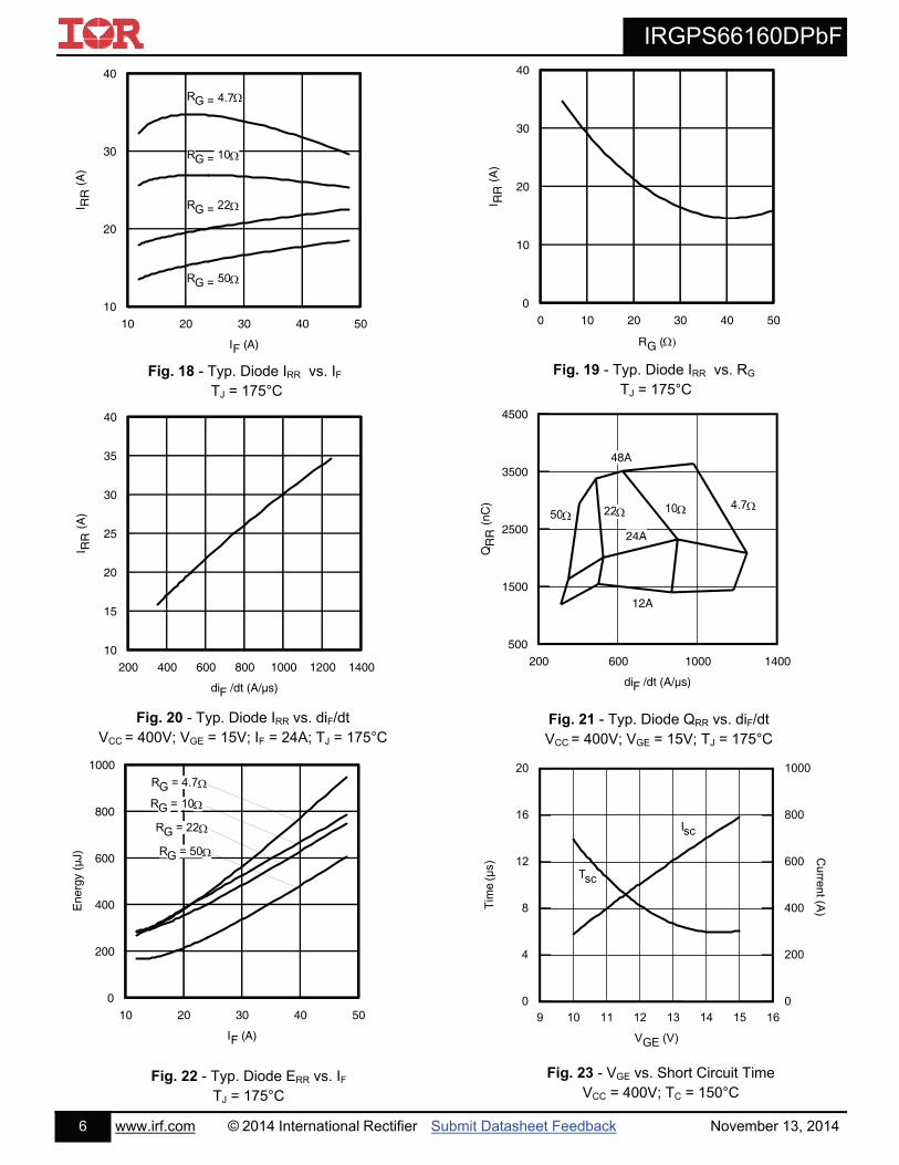
Fig. 22 - Typ. Diode ERR vs. IF TJ = 175°C
Fig. 21 - Typ. Diode QRR vs. diF/dt VCC = 400V; VGE = 15V; TJ = 175°C
Fig. 23 - VGE vs. Short Circuit Time VCC = 400V; TC = 150°C
10 20 30 40 50
IF (A)
10
20
30
40I R
R (
A)
RG = 50
RG = 10
RG = 4.7
RG = 22
0 10 20 30 40 50
RG (
0
10
20
30
40
I RR
(A
)
200 400 600 800 1000 1200 1400
diF /dt (A/µs)
10
15
20
25
30
35
40
I RR
(A
)
Fig. 18 - Typ. Diode IRR vs. IF TJ = 175°C
200 600 1000 1400
diF /dt (A/µs)
500
1500
2500
3500
4500
QR
R (
nC)
22 10504.7
24A
48A
12A
Fig. 19 - Typ. Diode IRR vs. RG TJ = 175°C
10 20 30 40 50
IF (A)
0
200
400
600
800
1000
Ene
rgy
(µJ)
RG = 10
RG = 4.7
RG = 50
RG = 22
Fig. 20 - Typ. Diode IRR vs. diF/dt VCC = 400V; VGE = 15V; IF = 24A; TJ = 175°C
9 10 11 12 13 14 15 16
VGE (V)
0
4
8
12
16
20
Tim
e (µ
s)
0
200
400
600
800
1000
Cu
rrent (A
)
Tsc
Isc
6 www.irf.com © 2014 International Rectifier Submit Datasheet Feedback November 13, 2014

IRGPS66160DPbF
7 www.irf.com © 2014 International Rectifier Submit Datasheet Feedback November 13, 2014
Fig. 27 - Maximum Transient Thermal Impedance, Junction-to-Case (IGBT)
0 100 200 300 400 500 600
VCE (V)
10
100
1000
10000
100000
Cap
acita
nce
(pF
)
Cies
Coes
Cres
Fig. 24 - Typ. Capacitance vs. VCE VGE= 0V; f = 1MHz
0 50 100 150 200 250
Q G, Total Gate Charge (nC)
0
2
4
6
8
10
12
14
16
VG
E, G
ate-
to-E
mitt
er V
olta
ge
(V) VCES = 400V
VCES = 300V
Fig. 25 - Typical Gate Charge vs. VGE ICE = 120A
1E-006 1E-005 0.0001 0.001 0.01 0.1 1
t1 , Rectangular Pulse Duration (sec)
0.0001
0.001
0.01
0.1
1
The
rmal
Res
pons
e (
Z thJ
C )
0.20
0.10
D = 0.50
0.020.01
0.05
SINGLE PULSE( THERMAL RESPONSE )
Notes:1. Duty Factor D = t1/t22. Peak Tj = P dm x Zthjc + Tc
J
J
1
12
23
3
R1
R1R2
R2R3
R3
Ci= iRiCi= iRi
C
C
4
4
R4
R4
Ri (°C/W) i (sec)
0.00487 0.000014
0.05032 0.000114
0.09091 0.003734
0.05519 0.017034
100 125 150 175
Case Temperature (°C)
0
40
80
120
160
200
Rep
etiti
ve P
eak
Cur
rent
(A
)
D=0.3
D=0.2
D=0.1
Fig 26. Maximum Diode Repetitive Forward Peak Current vs. Case Temperature

IRGPS66160DPbF
Fig. 28 - Maximum Transient Thermal Impedance, Junction-to-Case (DIODE)
1E-006 1E-005 0.0001 0.001 0.01 0.1 1
t1 , Rectangular Pulse Duration (sec)
0.0001
0.001
0.01
0.1
1
10
The
rmal
Res
pon
se (
Z th
JC )
0.200.10
D = 0.50
0.020.01
0.05
SINGLE PULSE( THERMAL RESPONSE )
Notes:1. Duty Factor D = t1/t22. Peak Tj = P dm x Zthjc + Tc
J
J
1
12
23
3
R1
R1R2
R2R3
R3
Ci= iRiCi= iRi
C
C
4
4
R4
R4
Ri (°C/W) i (sec)
0.02893 0.000034
0.43845 0.000326
0.60287 0.003626
0.30143 0.02205
8 www.irf.com © 2014 International Rectifier Submit Datasheet Feedback November 13, 2014

IRGPS66160DPbF
Fig.C.T.1 - Gate Charge Circuit (turn-off) Fig.C.T.2 - RBSOA Circuit
Fig.C.T.3 - S.C. SOA Circuit Fig.C.T.4 - Switching Loss Circuit
Fig.C.T.5 - Resistive Load Circuit Fig.C.T.6 - BVCES Filter Circuit
0
1K
VCCDUT
L
L
Rg
80 V
DUT VCC
+-
DC
4X
DUT
VCC
RSH
L
Rg
VCCDUT /DRIVER
diode clamp /DUT
-5V
Rg
VCCDUT
R = VCC
ICM
G force
C sense
100K
DUT0.0075µF
D1 22K
E force
C force
E sense
9 www.irf.com © 2014 International Rectifier Submit Datasheet Feedback November 13, 2014

IRGPS66160DPbF
Fig. WF1 - Typ. Turn-off Loss Waveform @ TJ = 175°C using Fig. CT.4
Fig. WF2 - Typ. Turn-on Loss Waveform @ TJ = 175°C using Fig. CT.4
Fig. WF4 - Typ. S.C. Waveform
@ TJ = 150°C using Fig. CT.3
Fig. WF3 - Typ. Diode Recovery Waveform @ TJ = 175°C using Fig. CT.4
-30
0
30
60
90
120
150
180
210
-100
0
100
200
300
400
500
600
700
-0.7 -0.2 0.3 0.8 1.3I C
E(A
)
VC
E(V
)
time(µs)
90% ICE
10% VCE
10% ICE
Eoff Loss
tf
-30
0
30
60
90
120
150
180
210
-100
0
100
200
300
400
500
600
700
-0.7 -0.2 0.3 0.8 1.3
I CE
(A)
VC
E(V
)
time (µs)
TEST CURRENT
90% ICE
10% VCE
10%ICE
tr
Eon Loss
-40
-30
-20
-10
0
10
20
30
-0.20 0.00 0.20 0.40 0.60
I F(A
)
time (µS)
PeakIRR
tRR
QRR
-100
0
100
200
300
400
500
600
700
800
900
-100
0
100
200
300
400
500
600
700
800
900
-4.0 0.0 4.0 8.0
Ice
(A)
Vce
(V
)
Time (uS)
VCE
ICE
10 www.irf.com © 2014 International Rectifier Submit Datasheet Feedback November 13, 2014

IRGPS66160DPbF
Super 247 Package Outline Dimensions are shown in millimeters (inches)
Super 247 Part Marking Information
11 www.irf.com © 2014 International Rectifier Submit Datasheet Feedback November 13, 2014
Note: For the most current drawing please refer to IR website at http://www.irf.com/package/
Super 247 package is not recommended for Surface Mount Application.
ASSEMBLY LOT CODE
TOP
EXAMPLE: THIS IS AN IRFPS37N50A WITH ASSEMBLY LOT CODE 1789
INTERNATIONAL RECTIFIER LOGO
89
IRFPS37N50A
17
PART NUMBER
ASSEMBLED ON WW 19, 1997IN THE ASSEMBLY LINE "C"
Note: "P" in assembly line positionindicates "Lead-Free"
719C
DATE CODEYEAR 7 = 1997WEEK 19LINE C

IRGPS66160DPbF
IR WORLD HEADQUARTERS: 101 N. Sepulveda Blvd., El Segundo, California 90245, USA To contact International Rectifier, please visit http://www.irf.com/whoto-call/
Qualification Information†
Qualification Level Industrial
Super 247 N/A
RoHS Compliant Yes
Moisture Sensitivity Level
† Qualification standards can be found at International Rectifier’s web site: http://www.irf.com/product-info/reliability/
†† Applicable version of JEDEC standard at the time of product release.
Revision History Date Comments
Added IFM Diode Maximum Forward Current = 480A with the note on page 1.
Removed note from switching losses test condition on page 2. 11/13/2014
12 www.irf.com © 2014 International Rectifier Submit Datasheet Feedback November 13, 2014