Embed Size (px)
Citation preview
Introduction to MEMS(Lecture 5)
Prof. Dong-Weon LeeMEMS & Nanotechnology Laboratory
School of Mechanical Systems EngineeringChonnam National University
http://love.chonnam.ac.kr/[email protected]
Today
1. Wafer production
2. Crystal: Silicon
3. Wafer identification
4. Process overview
5. Photolithography
6. Alternative technologies for lithography ???

http://love.chonnam.ac.kr/[email protected]
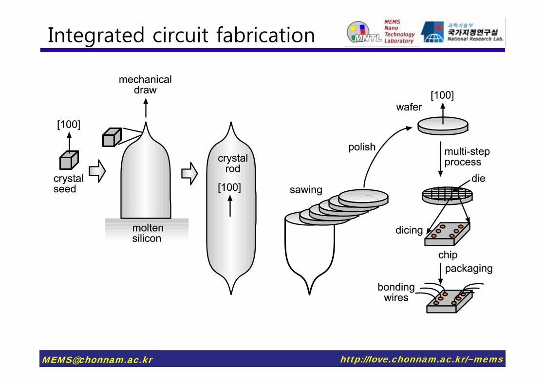
Silicon ingot
http://www.youtube.com/watch?v=cYj_vqcyI78http://www.youtube.com/watch?v=LWfCqpJzJYM&feature=related

http://love.chonnam.ac.kr/[email protected]
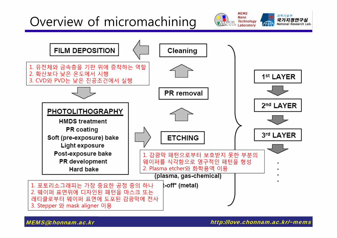
Overview of micromachining
1. 유전체와 금속층을 기판 위에 증착하는 역할2. 확산보다 낮은 온도에서 시행3. CVD와 PVD는 낮은 진공조건에서 실행
1. 유전체와 금속층을 기판 위에 증착하는역할2. 확산보다 낮은 온도에서 시행3. CVD와 PVD는 낮은 진공조건에서실행
1. 유전체와 금속층을 기판위에 증착하는 역할2. 확산보다 낮은 온도에서시행3. CVD와 PVD는 낮은
http://love.chonnam.ac.kr/[email protected]
Overview of micromachining
1. 포토리소그래피는 가장 중요한 공정 중의 하나2. 웨이퍼 표면위에 디자인된 패턴을 마스크 또는래티클로부터 웨이퍼 표면에 도포된 감광막에 전사3. Stepper 와 mask aligner 이용
1. 감광막 패턴으로부터 보호받지 못한 부분의웨이퍼를 식각함으로 영구적인 패턴을 형성2. Plasma etcher와 화학용액 이용
1. 유전체와 금속층을 기판 위에 증착하는 역할2. 확산보다 낮은 온도에서 시행3. CVD와 PVD는 낮은 진공조건에서 실행

http://love.chonnam.ac.kr/[email protected]
Clean room
Originally developed by NASA and the aerospace industry for satellite manufacturing. Clean rooms now in use for all MEMS and semiconductor manufacturing.

http://love.chonnam.ac.kr/[email protected]
DI water
• Water is the most prevalently used material in microfabricationprocesses, and is used mainly for rinsing and cleaning of wafers
• Approximately 6000 gallons of de-ionized(DI) water are required for each 6” CMOS wafer
• DI water must be manufactured on site to achieve the quality and purity levels required by modern microfabrication
• Each gallon of DI water may require as much as 4-6 gallons of raw city grade water to manufacture.
• DI water must be continuously recirculated in order to achieve the quality and purity levels
Clean water: de-ionized water

http://love.chonnam.ac.kr/[email protected]
HEPA filter
How Big of a Particle is Tolerable?– Example: 0.5 m CMOS technology
• Lateral Features:– pattern size = 0.5 m– pattern tolerance = 0.15 m– level-level registration = 0.15 m
• Vertical Features:– gate oxide thickness = 10 nm– film thicknesses = 250-500 nm– junction depths = 50-150 nm
Clean Room Air Filters• High Efficiency Particulate Air (HEPA) Filters
– most common type of clean room air filter– high efficiency, low pressure drop, good loading characteristics– uses glass fibers in a paper-like medium– are rated by their particle retention:
• A true HEPA-rated filter will retain 99.97 % of incident particles of 0.3 m.

http://love.chonnam.ac.kr/[email protected]
Characteristics of cleanroom
– Air is recirculated through HEPA filters with about 20 % make up• Vapors are entrained, so contamination potential is very high• Extensive gas detection and alarm systems are installed
– Temperature is controlled to 68 - 72 °F (20 ~ 22 °C)
– Humidity is controlled to 40 - 46 % RH
– Room is held at positive pressure• Typically 0.1 in H2O for Class 100, Class 1000, and Class 10,000• Positive pressure constantly blows dust OUT(Biohazard rooms operate at negative pressure to keep bugs IN)
• Doors open inward, so room pressure closes them shut• 0.1 in H2O = 3.6 x 10⁻³ psi = 0.52 lb/ft2
• This produces 9.1 lbs.(4.13kg) force on a 7’ x 30” door

http://love.chonnam.ac.kr/[email protected]
Types of cleanroom
Laminar Flow CleanroomTurbulent Cleanroom

http://love.chonnam.ac.kr/[email protected]
Dos and don’t in cleanroom
• Don’t:– touch your face or skin with gloves– touch building hardware, oily machinery, or wafer loading areas– lean on equipment– wear cosmetics, powders, or colognes– wear anything on fingers-- remove all rings and bracelets– use paper, pencils or markers that leave dust or lint
• Do:– change gloves whenever they get dirty or torn– use a fresh pair of gloves whenever handling wafers– wipe down wafer handling areas with isopropanol– use clean room paper and dust-free ball point pens

http://love.chonnam.ac.kr/[email protected]
기본적인 Cleaning 개념
유기물 제거 산화막 제거금속불순물 제거
이온성 불순물 제거 입자성 불순물 제거
산화막 제거 DI water Dry
RCA 1 (Organic dirt)
DI water(5):NH4OH(1), in a Pyrex beaker, and then heat to 70±5C on hot plate. Remove from hot plate and add a part of H2O2. Solution will bubble vigorously after 1–2 minutes, indicating that it is ready for use.
RCA 2 (metal ions: Au, Cu, Cr, Na etc.)
DI water(6):HCl(1) in a Pyrex beaker, and then heat to 70±5C on hot plate. Remove from hot plate and add 1 part of H2O2. Solution will bubble vigorously after 1–2 minutes, indicating that it is ready for use.
Cleaning process : wafer
RCA 1
RCA 2

http://love.chonnam.ac.kr/[email protected]
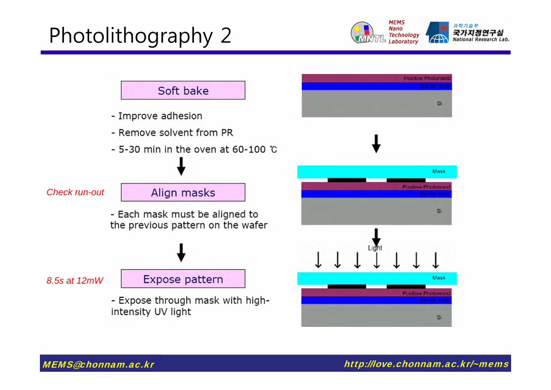
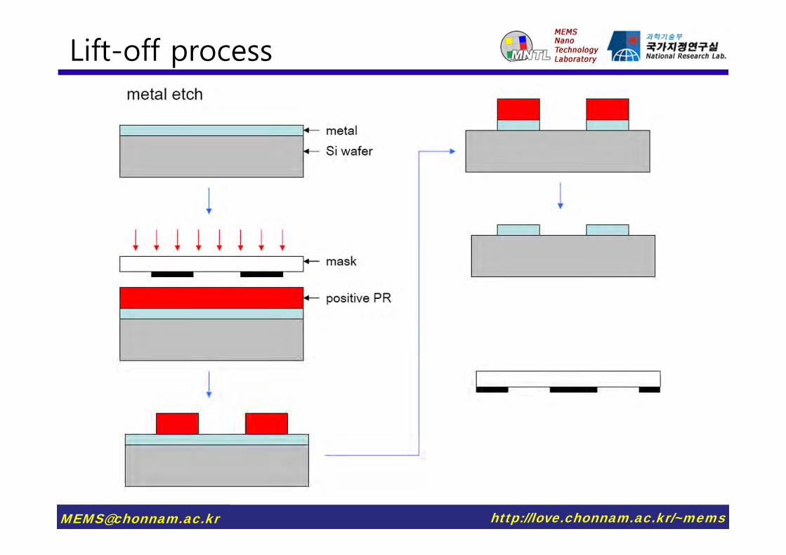
Steps in photolithography
1. Wafer cleaning
2. Apply adhesion promoter (HMDS)
3. Spin coat photoresist at 1000 – 10,000 rpm
4. “Soft bake” (90 – 120°C for 60 –120 sec) to remove solvent
5. Alignment
6. Exposure
7. Development
8. “Post bake” (100 – 180°C) to increase adhesion
9. Etch exposed regions
10. Strip resist
http://www.youtube.com/watch?v=9x3Lh1ZfggM&feature=related

http://love.chonnam.ac.kr/[email protected]
Key steps in photolithography
Photolithography: transfer patterns from a mask into photoresist

http://love.chonnam.ac.kr/[email protected]
Mercury bulbs (Hg Arc Lamp)
High pressure Hg Arc lamp spectrum

http://love.chonnam.ac.kr/[email protected]
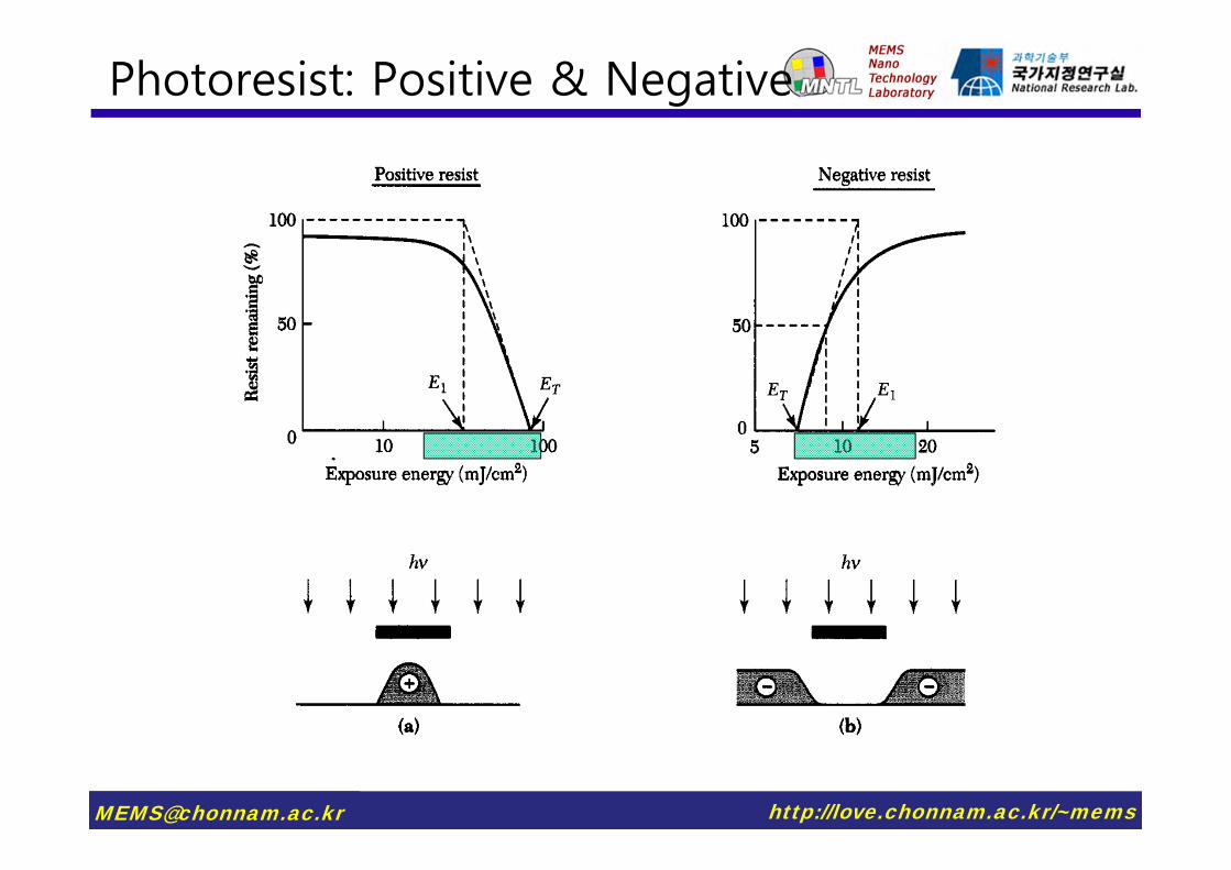
PhotolithographyPositive: gets more soluble after exposure
Negative: gets less soluble after exposure.
http://love.chonnam.ac.kr/[email protected]
Photoresist
- Photoresist is an organic polymer which becomes soluble when exposed or non-exposed to ultraviolet light (UV)
http://love.chonnam.ac.kr/[email protected]
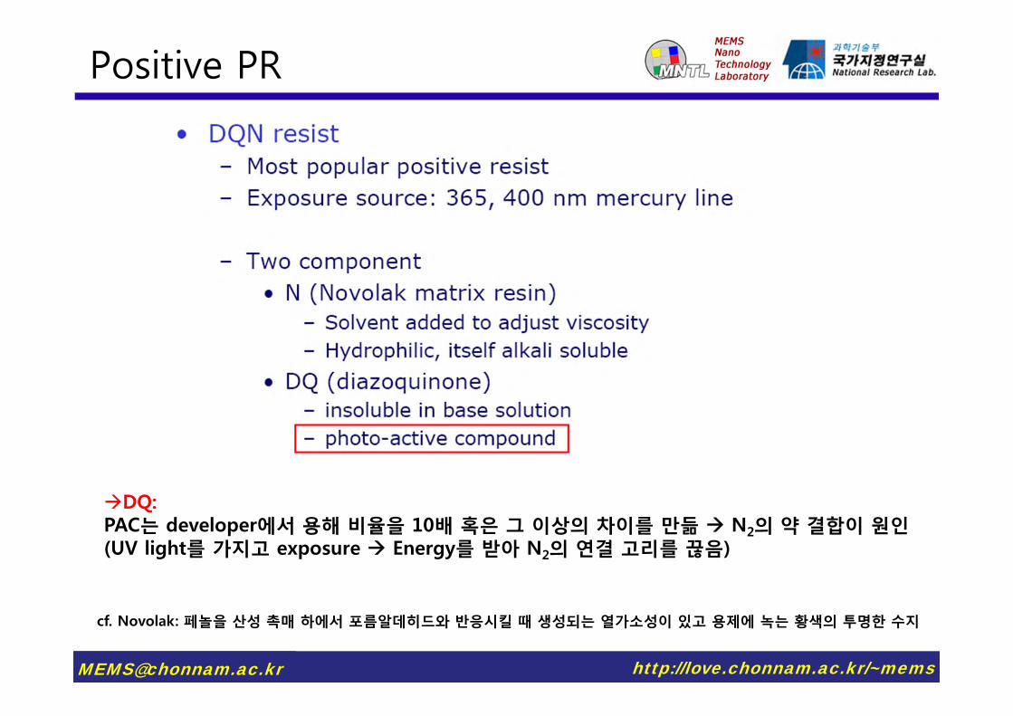
Positive PR
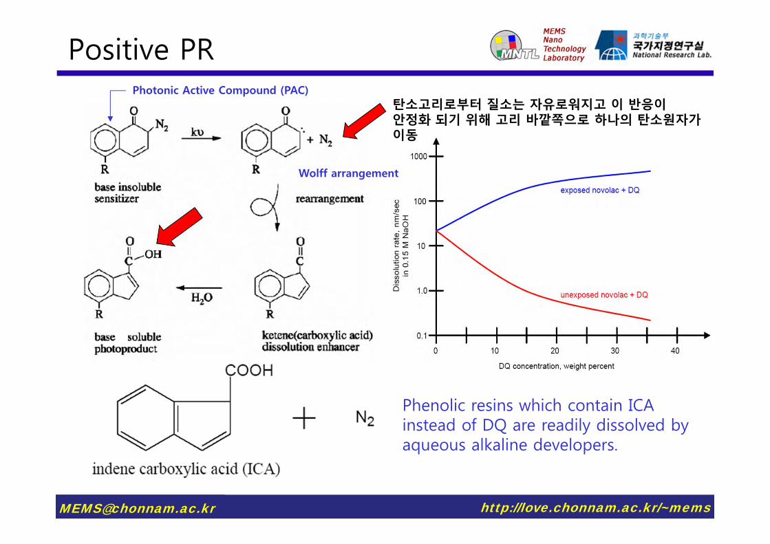
DQ:PAC는 developer에서 용해 비율을 10배 혹은 그 이상의 차이를 만듦 N2의 약 결합이 원인(UV light를 가지고 exposure Energy를 받아 N2의 연결 고리를 끊음)
cf. Novolak: 페놀을 산성 촉매 하에서 포름알데히드와 반응시킬 때 생성되는 열가소성이 있고 용제에 녹는 황색의 투명한 수지
http://love.chonnam.ac.kr/[email protected]
Phenolic resins which contain ICA instead of DQ are readily dissolved by aqueous alkaline developers.
Photonic Active Compound (PAC)
Wolff arrangement
탄소고리로부터 질소는 자유로워지고 이 반응이안정화 되기 위해 고리 바깥쪽으로 하나의 탄소원자가이동
Positive PR
http://love.chonnam.ac.kr/[email protected]
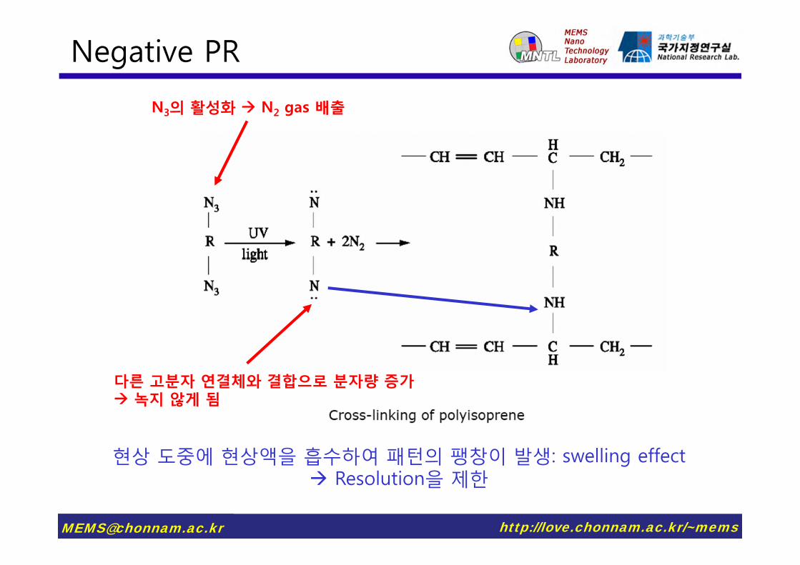
Negative PR
N3의 활성화 N2 gas 배출
다른 고분자 연결체와 결합으로 분자량 증가 녹지 않게 됨
현상 도중에 현상액을 흡수하여 패턴의 팽창이 발생: swelling effect Resolution을 제한

http://love.chonnam.ac.kr/[email protected]
Spin coating process
- Thickness of the photoresist depends on Concentration, Viscosity, Spin speed, Spin time
Spin speed
PR
thic
knes
s
Spin timePR
th
ickn
ess
- Photolithography stepsPhotoresist spinning, 1 to 50 mm spin coatOptical exposure through a photomaskDeveloping to dissolve exposed or unexposed resistBake to drive off solvents

http://love.chonnam.ac.kr/[email protected]
Photolithography 1: make a check list
Piranha, RCA 1 and RCA 2 cleaning
Ex. AZ 15121.2 m at 4000 rpm

http://love.chonnam.ac.kr/[email protected]
Soft bake목적: 용제(solvent)를 증발시켜 감광막을 건조시키고, 웨이퍼와의 접착력을 향상시키며, 열에 의한annealing effect로 응력을 완화장비Convection oven: 10 ~ 30분, 모든 웨이퍼에 동일 온도 유지 가능Infra-red oven: 3 ~ 4분, 웨이퍼에 종류에 따른 반사 및 흡수의 차이로 동일 온도 유지가 어려움Hot-plate: 0.5 ~ 1분, 가장 단시간에 가능, 진공흡착 등의 장비가 필요적정온도 유지 필요: 과소 Orange peel (Nega), mask 접착 (Posi, Nega)
과대 열 다중화에 의한 Scum 현상
Pattern size가 줄어들수록 soft bake의 온도와 시간은 매우 중요한 변수가됨
Photolithography 3
http://love.chonnam.ac.kr/[email protected]
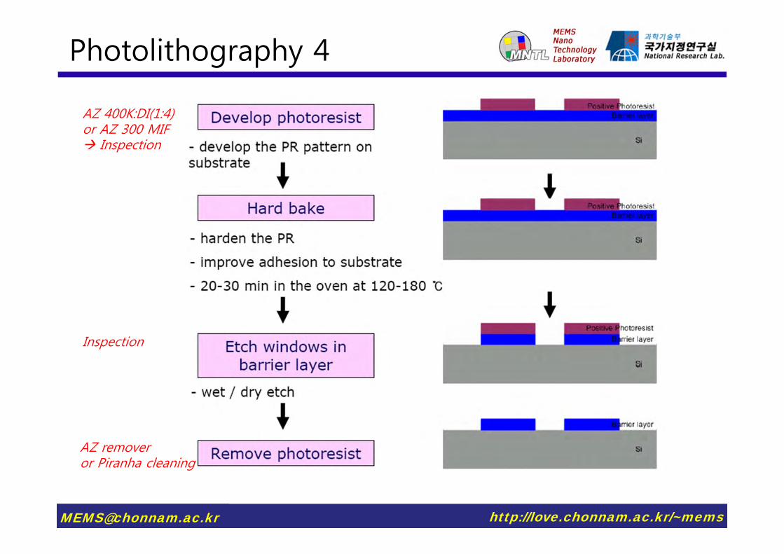
AZ 400K:DI(1:4)or AZ 300 MIF Inspection
AZ removeror Piranha cleaning
Inspection
Photolithography 4
http://love.chonnam.ac.kr/[email protected]
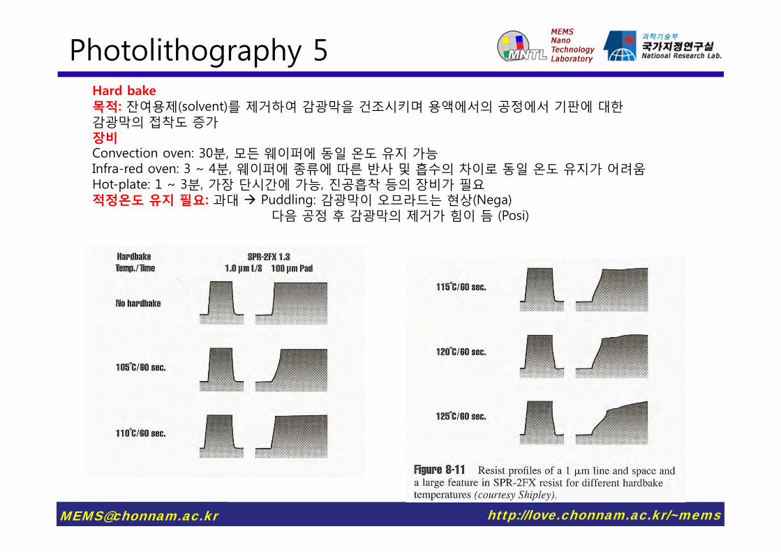
Hard bake목적: 잔여용제(solvent)를 제거하여 감광막을 건조시키며 용액에서의 공정에서 기판에 대한감광막의 접착도 증가장비Convection oven: 30분, 모든 웨이퍼에 동일 온도 유지 가능Infra-red oven: 3 ~ 4분, 웨이퍼에 종류에 따른 반사 및 흡수의 차이로 동일 온도 유지가 어려움Hot-plate: 1 ~ 3분, 가장 단시간에 가능, 진공흡착 등의 장비가 필요적정온도 유지 필요: 과대 Puddling: 감광막이 오므라드는 현상(Nega)
다음 공정 후 감광막의 제거가 힘이 듬 (Posi)
Photolithography 5
http://love.chonnam.ac.kr/[email protected]
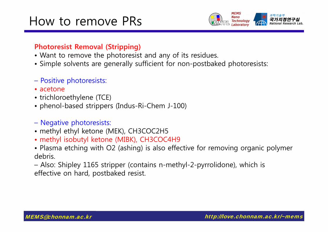
How to remove PRs
Photoresist Removal (Stripping)• Want to remove the photoresist and any of its residues.• Simple solvents are generally sufficient for non-postbaked photoresists:
– Positive photoresists:• acetone• trichloroethylene (TCE)• phenol-based strippers (Indus-Ri-Chem J-100)
– Negative photoresists:• methyl ethyl ketone (MEK), CH3COC2H5• methyl isobutyl ketone (MIBK), CH3COC4H9• Plasma etching with O2 (ashing) is also effective for removing organic polymer debris.– Also: Shipley 1165 stripper (contains n-methyl-2-pyrrolidone), which is effective on hard, postbaked resist.

http://love.chonnam.ac.kr/[email protected]
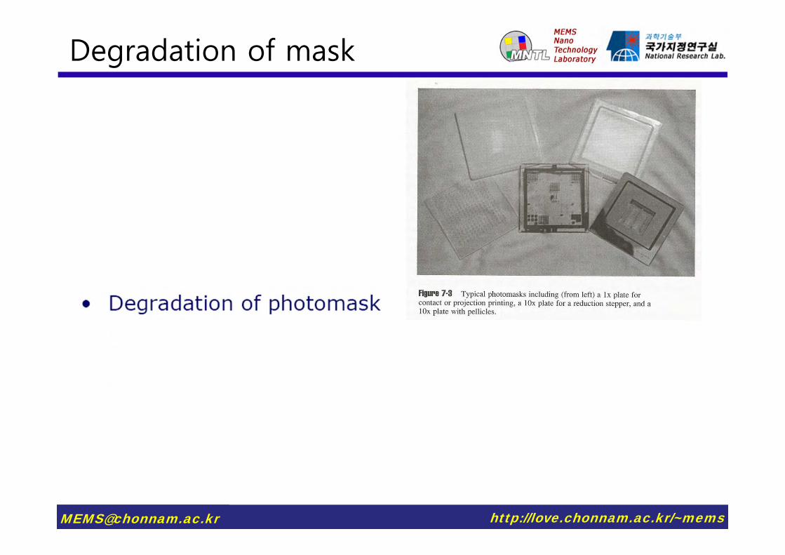
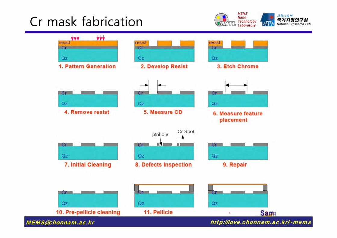
Photomask
- PhotomasksLayout generated from CAD file (GDSⅡ file)Mask reticle: chrome or emulsion on a glass or a quartz1-3 $k depends on mask materials
• Types:– film mask (200$/mask, cheapest)– photographic emulsion on soda lime glass– Fe2O3 on soda lime glass– Cr on soda lime glass– Cr on quartz glass (2000$/mask, most expensive, needed for deep UV litho)• Dimensions:– 4” x 4” x 0.060” for 3-inch wafers– 5” x 5” x 0.060” for 4-inch wafers• Polarity:– “light-field” = mostly clear, drawn feature = opaque– “dark-field” = mostly opaque, drawn feature = clear
http://love.chonnam.ac.kr/[email protected]
Limitation of UV-based litho.
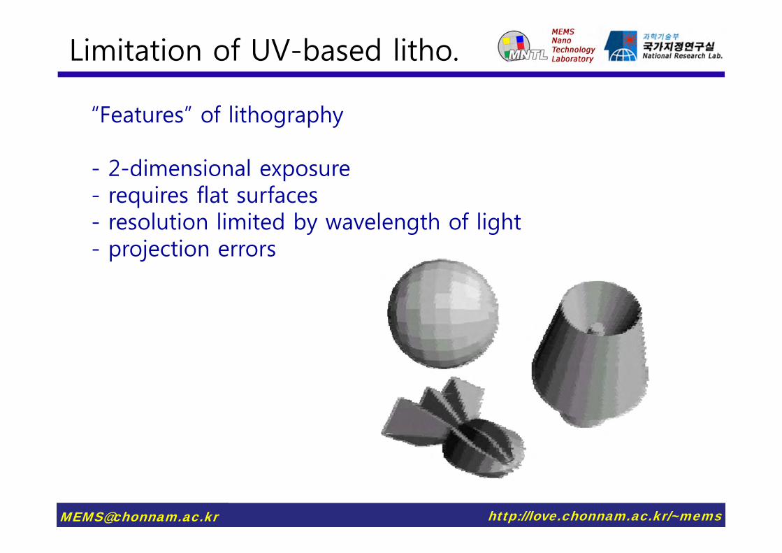
“Features” of lithography
- 2-dimensional exposure- requires flat surfaces- resolution limited by wavelength of light- projection errors

http://love.chonnam.ac.kr/[email protected]
Alignment process (P: Positive, N: Negative, A/B/C mask grade)
Mask to wafer align

http://love.chonnam.ac.kr/[email protected]
• Usually takes 1-5 seconds to align and expose on a modern stepper.• Human operators usually take 30-45 seconds with well-designed alignment marks.
Mask to wafer align

http://love.chonnam.ac.kr/[email protected]
Mask to wafer alignMultiple patterned layers of different materials
Report: Design of alignment marks (in case of 4 inch wafer)필요성, 작성방법, 위치, 어떠한 패턴을 이용하는지?, mark 크기 및 다양성, other considerations

http://love.chonnam.ac.kr/[email protected]
SPM-based lithographyDiameter Range 10 - 30 nm
Nanotube Length Range 500 - 3000 nm
Tip Angle +/- 5 deg
Resonant Frequency 300 KHz
Spring Constant 40 N/m
Cantilever Length 125 um
Reflective coating 30 nm Al on cantilever

http://love.chonnam.ac.kr/[email protected]
Summary: MEMS design & fabrication
Device/system design:Mechanics, electronics, electrostatics, fluidics
System analysis:Modeling, simulation
Process design:Chemistry and physics of fabrication
Fabrication:Clean room
Device/system testing:Microscope, probe station, SEM, laser vibrometer system, electronics
Problem;Compare with IC industry:No single standard process
Mask fabrication(1000 $/5 inch)