Embed Size (px)
Citation preview

INTEGRATED OPTICAL COMPONENTS PRODUCEDIN GaAs AND InP EPITAXIAL LAYERS USING
TRE PROTO-ELASTIC EFFECT
By
Trevor Mark Benson
A thesis presented for the Degreeof Doctor of Philosophy, Universityof Sheffield, Department ofElectronic and ElectricalEngineering, September 1982.

TEXTCUT OFF IN THE
ORIGINAL

SUMMARY
Studies have been made of optical waveguides produced
in GaAs and InP epitaxial layers. Of the possible waveguiding
mechanisms present in these devices the contribution from the
photo-elastic effect (strain-induced refractive index changes)
dominates. Stresses in evaporated metal films and their
control have been investigated.
Strain-induced waveguides have been used to produce a
novel directional-coupler structure with a short coupling
length (~2mm). In GaAs bias has been applied to control the
amount of light at the output of each of the two waveguides
forming these couplers and it has been possible to isolate
the light in either the excited or the coupled waveguide.
A new theoretical model, based on finite difference
techniques, has been developed and used to analyse strain-
induced, slab and rib waveguide structures. Results obtained
have been compared with those from other methods. Theoretical
predictions of guiding properties in GaAs strain-induced wave-
guides give good agreement with experimental results in all
cases. Optical waveguiding in InP layers using the same photo-
elastic mechanisms, assessed experimentally, indicates that
the refractive index changes are similar to those in GaAs but
slightly larger. One of the first measurements of the non-
zero electro-optic coefficient, r~l, of InP is described.
Guiding properties vary little with time in both InP and GaAs.
The reflection of light guided in a single-mode photo-
elastic waveguide into a second perpendicular guide using a

vertical etched facet running at 450 to the direction of
propagation is proposed for providing bending with negligible
loss and some experimental results are reported.

ACKNOWLEDGEMENTS
The author is indebted to Professor P.N. Robson and
Dr. P.A. Houston for their invaluable help and enthusiastic
supervision of this project.
It is a pleasure to thank Drs. D.H. Newman, S. Ritchie,
M.W. Austin, L.D. Westbrook and A.J. Houghton at British
Telecom Research Laboratories, Martlesham Heath for many
stimulating discussions and helpful suggestions and for the
provision of InP and GaAs epitaxial material. The kindness
of Dr. D. Ashen of R.S.R.E., Dr. J. Roberts and Mr. J.H. Marsh
in growing material is gratefully acknowledged.
Special thanks are due to Dr. T. Murotani of the
Mitsubishi Electrical Corporation for advice and assistance
with InP device fabrication and to Dr. J. Buus of the Technical
University of Denmark for enlightening conversations on the
effective refractive index method. Dr. T. Searle of the
Department of Physics is also thanked for the loan of equipment.
Expert technical assistance received under the leader-
ship of Mr. P.G. Ridsdale, Mr. R. Cousin, Mr. I. Moulson and
Mr. H. Flower is very much appreciated. In addition the author
thanks many members of the academic staff and fellow research
students for help and advice.
The author's gratitude is extended to Mrs. B. Cowell
for her patience and diligence in typing this thesis swiftly
and accurately.
The work reported here was carried out under an SERC

CASE studentship in collaboration with British Telecom and
the author extends his thanks for this financial support.

PUBLISHED WORK
The following papers have been published on the results
of some of the work described in this thesis.
1. "Photoelastic Optical Directional Couplers in EpitaxialGaAs Layers".T.M. Benson, T. Murotani, P.A. Houston, P.N. Robson.Electronics Letters, 17, 237, 1981.
2. "Photoelestic Optical Waveguiding in InP Epitaxial Layers".T.M. Benson, T. Murotani, P.N. Robson, P.A. Houston,Presented at the 7th European Conference on OpticalCommunication, Copenhagen, Sept. 1981.Published in Conference Proceedings as Paper 9.4.
3. "Photoelastic Optical Directional Couplers in EpitaxialGaAs Layers at 1.15~m".T.M. Benson, T. Murotani, P.N. Robson, P.A. Houston.Presented at the 1st European Conference on IntegratedOptics, London, Sept. 1981.
4. "A Novel Electro-optically Controlled Directional CouplerSwitch in GaAs Epitaxial Layers at l.l5~m".T.M. Benson, T. Murotani, P.N. Robson, P.A. Houston.Accepted for publication in IEEE Transactions on ElectronDevices for the Special Issue on Optoelectronic Devices,Sept. 1982.

CONTENTS Page No.
CHAPTER 1 - INTRODUCTION 1
CHAPTER 2 - GUIDED-WAVE OPTICS 6
2.1 Dielectric Slab Waveguide2.1.1 Ray optical treatment of slab
waveguides2.1.2 Fundamentals of the electromagnetic
theory of dielectric waveguides
6
7
10
2.2 Three-Dimensional Waveguides2.2.1 Analysis of rectangular waveguides2.2.2 Effective index analysis of
directional couplers
121216
2.3 Finite Difference Calculations 172.3.1 The method of successive over-
relaxation 202.3.2 Higher-order modes 21
2.3.2.1 Orthogonality of the waveguidemodes 22
2.3.2.2 Higher-order modes 232.3.3 Finite difference solution of the
one-dimensional wave-equation 25
CHAPTER 3 - THIN FILM STRESSES AND THE PHOTO- 26ELASTIC EFFECT
3.1 Thin Film Stresses 263.1.1 Intrinsic and thermal stresses 263.1.2 Experimental determination of thin
film stresses 283.1.3 Experimental results and discussion 30
3.2 Strain Due to Discontinuities in the MetalFilms and the Photo-Elastic Effect 34
CHAPTER 4 - DEVICES AND THEIR FABRICATION 39
4.1 GaAs Devices 39
4.1.1 Stripe waveguides 414.1.2 Channel waveguides - novel directional-
coupler structures 434.1.3 Conventional channel-waveguide
directional-coupler structures 444.1.4 Bends through 900 45
4.1.4.1 Etching of the (lOa) surface in GaAs 464.1.4.2 Fabrication of waveguides 48

4.2 InP Waveguides
4.3 Cleaving and Mounting Devices4.3.1 Cleaving4.3.2 Mounting on headers
CHAPTER 5 - THE OPTICAL EQUIPMENT
5.1 The Optical Bench
5.2 Waveguide Coupling
5.3 The Detection System
CHAPTER 6 - RESULTS AND DISCUSSION6.1 The Finite-Difference Method and its
Comparison with some other Techniques6.2 Attenuation in Dielectric Waveguides6.3 Guiding Mechanisms in Metal Clad
Waveguides6.4 The Finite-Difference Method for
Strain Waveguides6.4.1 Slab waveguides6.4.2 Convergence of the finite-
difference method6.5 GaAs
6.5.16.5.26.5.3
WaveguidesGuiding at a remote metal edgeStripe waveguidesChannel (slot or metal-gap)waveguides - novel directional-coupler structuresSingle-mode channel waveguidesin close proximityEvaluation of 900 waveguiding
6.5.4
6.5.56.6 InP Devices
6.6.1 InP Schottky diodes6.6.2 InP waveguides
6.6.2.1 Stripe structures6.6.2.2 Channel structures
6.7 Strain-Induced Waveguiding With NoEpitaxial Layer
CHAPTER 7 - CONCLUSIONS
CHAPTER 8 - REFERENCES
Page No.
48
505050
52
52
53
53
55
5558
60
6262
62636366
69
79818282848485
86
95
98

Page No.
CHAPTER 9 - APPENDICES 104
9.1 Reflection of Plane Waves atPlane Interfaces
9.2 Computer Program For The Solution ofthe Eigenvalue Equation
9.3 Characteristic Equationsfor theEffective Index Analysis ofDirectional Couplers
9.4 Finite-Difference Form of PartialDerivatives
9.5 The Rayleigh Quotient9.6 A Method for Finding the Optimum
Acceleration Factor for S.O.R. (So)and a Practical Scheme ofComputer Solution
9.7 Loss in Waveguides9.8 Coupled Wave Theory of Directional-
Couplers
104
108
114
115116
118124
126

1.
CHAPTER 1
INTRODUCTION
Optical-fibre transmission has established itself as a
reliable and cost-effective technology capable of meeting the
rapidly increasing demand for high bit-rate communications.
Light as a carrier wave, modulated to carry data, offers an
enormous potential bandwidth for communications because of its
high frequency although practical bandwidth is limited by the
components of the fibre system.
The aim of integrated optics is to provide system
components such as switches, mixers and modulators using
light confined in thin dielectric films. The ultimate goal
is 'monolithic' integrated optics where light sources [1] and
detectors [2] are fabricated on the same substrate as the
other circuit components.
The simplest integrated optical components are passive
waveguides. These require the creation of a region with a
higher refractive index that its surroundings and can be
manufactured, for example, from glasses of different
composition[3]. To provide external control of the light in
the waveguide it is required to use materials in which local
refractive index changes can be induced via the electro-optic,
the acousto-optic or the magneto-optic effects. Of a host of
materials used to make individual devices [4] lithium niobate
(LiNb03) has the merits of a high electro-optic coefficient,
good acousto-optic properties and a well-developed technology
for waveguide formation based on titanium in-diffusion. It

2.
is unsuitable for monolithic integration, however, as no
LiNb03 source is available.
Gallium arsenide (GaAs) and related compounds therefore
hold a major advantage as sources in the right part of the
infra-red spectrum can be fabricated. GaAs based lasers or
light-emitting diodes (L.E.D's) are used as light sources for
multimode fibre systems installed world-wide [5],[6],[7].
The emitted wavelengths of 0.8-0.9~m enable silicon avalanche
photodiodes (A.P.D's) to be used as detectors.
By operating in a longer wavelength region (1.25-1.6~m)
fibre attenuation and material dispersion can be minimised [8].
The InGaAsP/lnP materials system has been exploited to produce
highly efficient light sources in this wavelength range.
Changing the composition alters the bandgap and hence the
emitting wavelength. More recent attention has been focussed
onto monomode fibre, where bandwidth is limited solely by
material chromatic dispersion, for higher transmission speeds
and longer distances [9],[10]. The chromatic dispersion of
silica fibre goes through a zero near 1.3~m and at this wave-
length there is no first-order limitation on bandwidth. The
continued improvement and acceptance of single-mode fibres
enhances the prospects for high data-rate systems employing
integrated optical terminal devices since the great majority
of integrated optical circuits and devices are single-mode
structures.
Direct modulation of semiconductor laser drive current
is the most convenient way of digital encoding. However,

3 •
under rapid modulation wavelength instability is
encountered [11]. Fast encoding by external guided-wave
modulators could overcome this limitation, allowing stable
continuous operation of the laser.
The electro-optic effect in GaAs allows for phase
modulation of TE propagating modes whereas TM modes are
unaffected. By exciting both TE and TM modes an external
analyser can be employed to convert the phase shift to
intensity modulation [12].
The directional-coupler switch provides for the modu-
lation of light in a waveguide by the transfer of the guided
light to a similar adjacent waveguide. The device length may
be chosen to give complete power transfer between the two
phase-synchronous guides. Field-induced refractive index
changes may then be used to destroy the phase synchronism
and thereby switch the light back to the initially excited
guide. The switching performance depends critically on the
phase matching between the waveguides and on device length.
Electro-optically controlled directional-coupler
(E.C.D.) switches have been fabricated in LiNb03 using in-
diffused waveguides [13] and in GaAs and GaAIAs using 'metal-
gap' guides [14], rib waveguides of the Schottky Barrier [15]
or M.O.S. [16] type and p+n-n+ channel-stop strip guides [17].
In the stepped ~8 reversal directional-coupler switch
[18] the sign of the refractive index step induced between
the two guides forming the directional coupler is reversed
halfway along the device. The advantage of multi-electrode

4.
pairs for a large-extinction ratio switch was first demonstrated
in LiNb03 [19]. In GaAs Leonberger and Bozler [20] reported
up to 99.7% cross-over (25dB) using a metal-gap structure with
two electrode pairs.
Modulator structures based on band-to-band absorption
effects at wavelengths near the bandgap [21] have also been
fabricated in GaAs but active Y-junction switches [22] and the
Mach-Zehnder interference modulator structure [23] have still
to be demonstrated in this material. Westbrook showed clearly
that passive single-mode optical waveguides can conveniently
be produced in GaAs epitaxial layers by strain-induced
refractive index changes [24]. In this thesis the nature of
the stress in evaporated metal films has been studied and the
findings of Westbrook confirmed. Ways in which the amount of
stress introduced may be controlled and time-dependent
annealing effects have been examined. Strain-induced wave-
guides have been used to produce a novel directional coupler
structure with a short coupling length (~2mm) and high
synchronism without rigid fabrication tolerances. It is also
shown that in GaAs waveguides formed by the epitaxy of low-
doped GaAs on a heavily-doped GaAs substrate strain-induced
refractive index changes must also be included to explain the
behaviour of 'metal-gap' E.D.C. devices.
A new theoretical model based on finite difference
techniques has been developed to analyse electromagnetic wave
propagation in waveguide structures in general but in the
inhomogeneous strain structures in particular. In addition
to using the technique to study strain waveguides a theoretical

5.
analysis of some rib-waveguide structures has been made to
allow comparison with other methods.
Optical waveguiding in InP layers using the same photo-
elastic mechanisms has been examined to assess possible
application to integrated optics in the long wavelength systems.
In GaAs guiding around bends has also been evaluated as
these will be essential for increasing device packing density
in envisaged integrated optical circuits. It is shown that
the refractive index changes forming the observed waveguides
are not large enough for fabricating curved waveguide sections
with radii of curvature comparable with integrated optics and
exhibiting tolerable loss. A method for forming bends in
waveguides by reflection off an etched vertical wall is
proposed therefore for providing waveguiding through a right
angle with negligible loss. Experimental results for thisstructure are presented.

6 •
CHAPTER 2
GUIDED-WAVE OPTICS
2.1 Dielectric Slab Waveguide
The dielectric slab form of optical waveguide,
illustrated in Fig.2.l, consists of a planar film of refractive
index n2 sandwiched between two regions with lower refractive
indices nl and n3 respectively. Light is confined by total
internal reflection at each of the material interfaces.
A study of the slab waveguide is useful in gaining an
understanding of the waveguiding properties of more complicated
dielectric waveguides. Its simple geometry enables the fipite
number of guided modes and the infinite number of radiation
modes to be described mathematically without difficulty and
obtained as solutions of boundary-value problems.
A ray-optical picture of light propagation in slab
waveguides is first outlined to gain a physical understanding.
Although this approach can provide a number of useful results
such as propagation constants and cut-off widths it is then
shown that a much more complete description is provided by
electromagnetic theory. The results obtained from the two
treatments are in complete agreement.
In the devices described in this thesis GaAs optical slab
waveguides are produced by growing epitaxial layers of n-
GaAs on an n+ GaAs substrate as in Fig. 2.2. The depression
of the refractive index 6n due to free carriers is given by [25]:
Ne2 A026n = (2.1)

z
-,"" n1o~------~~ ....------------------~~y""-'........"" n2
-h r=-':;__----------------
Fig.2.l Generalised dielectric slab waveguide showingnotation for axes and refractive indices.
Heavily doped+n -GaAs or InP
Low doped n-GaAsor InP
Fig.2.2 Slab waveguide due to free carriers as used inthis work.

7.
*where N is the number of free carriers per cubic metre, m
the carrier effective mass, e the electronic charge, Eo the
permittivity of free space, c the velocity of light in free
space, no the refractive index in the absence of free carriers
and Aa the free-space wavelength. Because of the large
difference between the doping levels the value of (n2-n3)
is taken as ~n for the substrate, calculated using (2.1).
Quality is good enough for material and interface perturbation
losses to be neglected.
2.1.1 Ray-optical treatment of slab waveguides
Consider the ray picture of Fig.2.3. For the guided
mode illustrated e must exceed the critical angles at both
interfaces to get total internal reflection. In the present
case therefore e must be greater than sin-1 (n3/n2), the
critical angle at P, since the critical angle at the substrate
interface is larger than the one at the air interface because
of the smaller refractive index difference.
The light trapped in the region of refractive index n2
may be considered to travel in a zig-zag path and, by
satisfying the requirement that the total phase shift sums to
2qn where q is an integer, the propagation constant 8 of a
guided mode may be found. S is related to the zig-zag angle
e by :-
(2.2)
where k = 2n/Ao.o
The critical angle and equation (2.2) produce bounds
for 8 such that :

NI .c0 I
~IIx
b'I'dNIb'.,-lN
(J)..c:4J
440til..-IcOe0s::
- --- (J):>ttl~b'.s:: (J).,-l '0~ g..c:
-- -- tIl'U(J)(J)'U'0 .,-l.,-l ::l::l b'0'1(J) I'd:>I'd 0~4J
,QO'II'd s::..-I.,-l1Il'Us::I'd 0
0..tH IIIo (J)
I-l~ I-l(J) 0.,-l u:>
III(J) (J)'0:>.,-l I'dU)~
M
N
N.., .
C C C b'.,-l~

8.
The determination of S requires knowledge of the phase
shifts 2¢s and 2¢c at the n2-n3 and n2-nl interfaces
respectively. In Appendix 9.1 expressions for the phase shifts
on reflection of a plane wave at plane interfaces are derived
for both TE and TM polarisations. It follows that in all cases
the angle ¢ is given by :-s
tan¢s = Jn22sin2e-n32/n2cose
for TE modes, and
(2.3)
jn22 sin2e-n32n2cose (2.4)
for TM modes. With nl replacing n3 the same relationships hold
for tan ¢c for a dielectric/dielectric interface between n2 and
the cover n 1.
Only a discrete set of angles e leads to a self-consistent
picture and "guided modes". Consider a guide cross-section
Z = constant and the phase shifts on moving from the x = -h
boundary to the one at x = 0 and then back with the reflected
wave. The total phase shift must equal a multiple of 2n for
self-consistency. Thus
2k n2hcose-2¢ -2¢ = 2qno s c (2.5)
where ¢ and ¢ are functions of e as mentioned.s c
From equations (2.2), (2.3) and (2.4)
2¢S = 2tan-1{ y 1 (S2-n / k 0 2)~ } (2 .6)n22ko2-S2
and 2¢ = 2tan-1{ y 3 (S2-n 12k 0 2)~ } (2.7)c n22ko2-S2

9 .
where2
Y. = (n2) for TM modes1. n.
1.
= 1 for TE modes
Defining
(2.8)
P 3 2 = B 2-n 3 2k 0 2
(2.5) becomes
q'IT (2.9)
Now kon2hcos8 = hq2 so,
(hq, -q'IT)
i.e.
tan (hq2-q'IT)= (~+~)q2 q2(1- Plp3YIY3)
q22
= g2 (Y IP 1+y 3P 3)
(q22-YIY3PIP3)(2.10)
(2.10) is an eigenvalue equation for the transverse propagationconstant q2.
For the case of a metal cover equations (2.3) and (2.4)
become (see Appendix 9.1)
(2.11)
for TE modes, andn2 (nc")2 cos8
(2.12)
for TM modes where nl = n l_jn " ~ -jn ".c c c

10.
2.1.2 Fundamentals of the electromagnetic theory ofdielectric waveguides
Maxwell's equations for time dependent fields in a
source-free region are :-
VxH =aDat (2.13)
aBVxE =-_.:_~ at (2.14)
V.H = 0 (2.15)
(2.16)'I.E = 0
where E, H, D and B are time dependent vectors of electric and~ ~ ~
magnetic field, electric displacement and magnetic induction
respectively.
Assume fields with a periodic time dependence of angular
frequency wand a loss less medium of dielectric constant £ and
permeability Uo. Now applying the curl operator to (2.14),using (2.13) to eliminate H and noting that B = UoH and D =EE gives :
a2E'Ix(VxE) = -UOE---at2
(2.17)
For any vector A
'Ix('VxA) = V(V.A)-V2A~ ~ ~
and using this) h.\\"'\ ~C'\~ ("4. .n) C"e..s\:.k1-.~, \.,\.
(2.18)
In the planar guide the modes are uniform in the y direction
so all derivatives with respect to yare zero. Assuming that
E = ni2Eo where i = 1,2,3 field solutions of the form

11.
E(x,y,z) = E (x,y)exp(-jB z)v v
can be found and may be interpreted as modes of the waveguide
with propagation constants B. The reduced form of the wave-vequation is :
(2.19 )
The remaining requirement is that tangential E and H fields be
continuous at the dielectric discontinuities. f=oC""-rE ~c)dQ.t;. \-'ne..
(\O~ .."te~o ~«...\~
('l..'~") ~~\c\.. ':Hx
BE= - -_y
w~o (2 .20)
and. dE
__L ____yw~o dX
(2.21)
For guided modes in slab waveguides power is largely confined
in the central layer of the guide which is satisfied for an
oscillatory solution in region 2 and evanescent tails in the
cladding regions. The field solutions obtained are :
E = Aexp (-p1x) x ~ 0y= A cos (q2X}+B.sin(q2x) 0 > x ~ -h
= [A cos (q2h)-Bsin (q2h)]exp{p 3 (x+h) }x< -h (2.22)
where A _SL=B P!
Pl, q2, P3r are as defined by (2.8) and q2 obeys the eigen-
value equation (2.10).
Similar forms of the wave-equation for the magnetic
field ~ may be derived from Maxwell's equations ~~ 1'tI\ t<\~~q_~.
Exact solutions of the eigenvalue equation (2.10) were

12.
obtained by a computer program listed in Appendix 9.2. For
the case where nI, n2 and n3 are real (lossless) the solution
is obtained by continuous bisection in the range (q-l)n <q2h
<qn where q is the solution number. In the case where nI, n2
or n3 are lossy the refractive index becomes complex and the
substitution of (n-jk) for n in (2.10) gives a complex form
of the eigenvalue equation. Numerical solution for the complex
propagation constants also yields the attenuation constants of
the guided modes. The computer program of Appendix 9.2 uses
Newton's method to solve the complex form of (2.10).
2.2 Three-Dimensional Waveguides
2.2.1 Analysis of rectangular waveguides
Propagation in the slab waveguide structures described
in section 2.1 has an exact mathematical solution. In many
applications, however, transverse waveguiding (that is in the
y direction) is also important. Examples of some of the types
of these three-dimensional waveguides have been discussed by
Kogelnik [26]. An exact analytical solution for such a
structure is not possible and for a rigorous solution to the
boundary value problem of a rectangular dielectric waveguide
recourse must be made to numerical analysis and the use of a
computer [27]. It is possible, however, to approximate the
problem by replacing it with two or more planar problems as
discussed in this section.
Consider the step-index rectangular waveguide config-
uration of Fig.2.4. The guiding region is the one with
refractive index n The propagation constant (S) for theml

"rt13
Fig.2.4 Waveguide cross-section subdivided for analysis bythe method of Marcatili [28]. Region i is thatwith refractive index n ..m1

13.
modes in this guide is given by
(32 = n 2 k 02 _q 2 _q 2ml x Y (2.23)
where n is the refractive index of the waveguide core andmlqx and qy are the transverse propagation constants.
The approximate analysis of Marcatili [28] is based on
the assumptions that field components in the two orthogonal
directions are independent of each other and at the edges of
the shaded regions of Fig.2.4 boundary conditions may be
relaxed. The simplification arises from observing that for
well guided modes the fields decay exponentially in regions
2-4. Therefore most of the power is contained in region 1,
a small part in regions 2-4 and little in the four shaded
regions. Clearly such an approximation holds only for modes
well guided with most of the light energy travelling in thewaveguide core.
Knox and Toulios [29] modified Marcatili's analysis
for modes which are less well guided by using an effective
refractive index to couple the two slab guides approximating
the original rectangular structure. The method is illustrated
in Fig.2.5 and was shown by the authors to give closer
agreement than Marcatili's method to the computer analysis of
Goell [27] near cut-off, a fact especially noticeable for
low-order modes. In practice the technique involves firstly
calculating the propagation constant of the slab guide formed
if one lets the long guide dimension approach infinity (Fig.2.5
(b». The propagation constant obtained (q ) is used toxdefine an effective refractive index, nefft, through

.+- a -----+I
y
tb+
ant3
bbt
I n
14-----.a-----..
m
c
Fig.2.5 Analysis of a rectangular dielectric waveguide bythe method of Knox and Toulios [29](a) Configuration of the waveguide(b) Slab waveguide with equivalent confinement
in the x direction(c) Equivalent slab guide with confinement in
the y direction. neff defined from (b).t

14.
n 2 k 2 = n 2k 2_q 2efft 0 tl 0 X (2.24)
A second slab guide is now formed filled with a material of
refractive index nefft by allowing the short guide dimension
to approach infinity (Fig.2.5(c». The propagation constant
of the slab guide so formed is taken as that representing theoriginal waveguide.
A slightly different approach has been applied to strip-
loaded guides by Furuta et al [30] and to metal-clad guides by
Yamamoto et al [31] who both use an equivalent refractive
index to reduce the structure to an equivalent rectangular
waveguide suitable for analysis by Marcatili's method.
The effective index approach has been further developed
by Itoh [32], McLevige et al [33] and Hamasaki and Nosu [34].
The assumption made by these authors is that if the aspect
ratio of the waveguide is large there is much strongerconfinement in the x direction shown in Fig. 2.5 and \("\~C2_wo.."~\k Co('c.. :
E (x,y) ~ E(y) cos{q .x + ~.}Y Xl 1 (2.25)
where i = I, II, III corresponds to the regions illustrated in
Fig. 2.5 (c).
The wave equation becomes
d2E__y + (k 2n.2 -q 2 -s 2) E = 0dy2 o 1 xi y
or using equation (2.24)
d2E__y + (k 2n 2 _(2)E = 0dy2 o effi y
(2.26)
(2.27)

15.
Thus the problem is finally reduced to solving analytically
the three dielectric slab regions (i = I, II, III), obtaining
an effective index for each region which together form a
lateral slab to be similarly solved. Intuitively a TM
solution in this composite guide would appear to be the
correct one but in practice there is very little difference
between TE and TM solutions as generally one is working a
long way from cut-off and the two modes are nearly degenerate.
The effective index analysis can be used in two ways
depending on which lateral propagation constant is calculated
first. A simple argument can be used to show that the method
is particularly useful if there is a large field variation
in one direction and a solution is first found for the larger
transverse propagation constant in the direction of strongest
guiding. The argument is based on the fact that the q and qx yterms in equation (2.23) may be regarded as perturbations on
then 2 ko2 term and in the effective index method the smallermlof q should be neglected to get a first-order approximationx,yto B which is subsequently improved.
The effective index method will be used in later sections
to analyse some waveguide properties. In particular the method
is compared in section 6.1 with results from computer solutions
for the case of rib waveguides of the configuration shown in
Fig.2.6. This particular structure cannot be analysed directly
by Marcatili's method because, although lateral waveguiding is
observed,there is no physical refractive index change in the
y direction.

n, '-,III
aII_.II
a)
x
'''' a-~_'~1I ][y
Ib)
Fig.2.6 Analysis of a general rib waveguide by theeffective index method.

16.
Buus [35] has also demonstrated good agreement of the
effective index method with a numerical method of calculation
[36] for semiconductor lasers having a gradual lateral
variation in complex permittivity.
2.2.2 Effective index analysis of directional couplers
An exact analytical solution for the coupling length
of rib and strain-induced directional-coupler structures isnot possible and again recourse must be made to a numerical
method or an approximate model lending itself to analytical
solution. A suitable approximation can be made using an
extension of the effective index method.
The device is divided into regions I, II, and III
shown in Fig.2.7 and, by assuming each region to be an infinite
slab in the y direction, effective guide indices NI' NIl and
NIII can be obtained as Si/ko where Si is the propagation
constant of the fundamental TE mode for each slab guide.
The coupling length is calculated by modelling the five-
layer structure of infinite extent in the x direction with
indices Ni' The coupling length, Lc' is taken as (Ss-BA)/n
where BS and BA are the propagation constants of the
symmetric and asymmetric TM modes of the double-guide system
(see Appendix 9.8). The characteristic equations for the
symmetric and asymmetric modes are (see Appendix 9.3)
tan[2aqz] *= ~{Y1Pl+Y3P3}{q22_Y1Y3P1P3* }
(2.28)
*where P3 = P3tanh{ P3(c-a)}
= P3/tanh{P3 (c-a)}
symmetric mode
asymmetric mode

I : I.---t--..-c-lI I I: I I
I
1I.
--2a-I
•--20-
I II
'-2Q .....I I
'-20--'I I
n :II II m
Fig.2.7 Analysis of a directional coupler by theeffective index method.

17.
NIl 2y. = (-)1 N.
1
i = I, III
and=N 2k"_S2
II 0
= 62 - NIII2ko"
2.3 Finite Difference Calculations
A method is described in this section for analysing
electromagnetic wave propagation in dielectric waveguides
where refractive index may vary in both directions of the
cross-section but is constant in the longitudinal direction
(assumed infinitely long).
The basis of the procedure used is to replace the wave
equation by finite difference relations in terms of the fieldsat discrete mesh points. Boundary conditions are enforced
by enclosing the waveguide within an arbitrarily determined
electric wall and full advantage taken of symmetry so that in
most of the structures studied only half the waveguide cross-
section is considered.
The finite difference techniques lead to a matrix
eigenvalue problem and the construction of a computer program
to calculate the field distribution and eigenvalue iteratively
is described here in detail.
The importance of finite difference methods lies in the
ease with which many operations and functions may be
represented. Operations are then performed somewhat approx-
imately in terms of values over a discrete set of points and
as the distance between points is made sufficiently small it

18.
is hoped that the approximation made becomes increasingly
accurate. As will become evident operations such as differ-
entiation and integration reduce to simple arithmetic forms
suitable for digital computation.
From equation (2.24) the wave equation for TE modes is
(2.29)
To apply the finite difference method the waveguide cross
section is cov~red with a rectangular mesh of size X and Y in
the x and y directions respectively. The different step
lengths were incorporated to facilitate the study of devices
with large aspect ratios. In place of the function Ey(X,y)
consider discrete values of E at mesh points only and replacey
the partial derivatives of (2.29) by the finite difference
expressions of Appendix 9.4.
Rearrangement of these expressions gives
E(I,J) = ~I+l,J)+E(I-l,J)+R2{E(I,J+l)+E(I,J-l)}2[l+R2]-ko2X2-{N2 (I,J)-N2}
(2.30 )
where R = X/Y, N(I,J) is the refractive index at the point
(IX,JY) and N is the effective refractive index of the guide.
Axes and dimensions were labelled as in Fig.2.8 giving
a waveguide of dimensions AX and 2BY with a centre line of
symmetry at J = 1. The following boundary conditions were
imposed :
E(O,J) = E(A,J) = E(I,B+l) = 0 (2.31)
Symmetry about the centre line was modelled by requiring

><
I
- _1- - - - - - - - -,- - - -. >
...-+en
-- --CW')
«:) _ N···Lj__j-.L------------;;_:-T - ---• ~ n~ ..,
L-~~+_------------------,_l----N
•N

19.
E(I,O) = E(I,2) for symmetric modes(2.32)
and E(l,l) = ° for asymmetric modes
It is shown in Appendix 9.5 that a variational
expression can be formed for the propagation constant S(=N/ko)
of the waveguide that yields a lower bound for 82 which
improves as the trial function for E approaches the actualymode distribution. This variational expression is the
Rayleigh Quotient and is
crosssection (2.33)
ff E 2 dxdyy
crosssection
A finite difference form of the Rayleigh Quotient is also
required. The integrand in the numerator is expressed as
E(I,J) {E(I+l,J) + E(I-l,J) - 2E(I,J)X2
+ E(I,J+l) + E(I,J-l-2E(I,J) + ko2N(I,J)E(I,J)}y2
::.:T(I,J) say (2.34)
The integration formula used to evaluate the numerator
and the denominator was the "trapezoidal rule" [37] since the
more accurate Simpson's 1/3 rule [37] was seen to give no
improvement in the solution of one-dimensional waveguides.
The trapezoidal rule gives :

20.
JJT(l,J)dXdYB A-I A-I T(l,l)= I I T(l,J)XY + I XY
J=2 1=1 1=1 2
= C sayand
J JEy2dxdyB A-I A-I 1..
= L }" LE ( I ,J)] 2 XY + }" E r r ,1) XYJ=2 1=1 1=1 2
= G say
(2.35)
(2.36)
If the value of the numerator is C and that of the denominator
G then from (2.33), (2.35) and (2.36)
(2.37)
from which a value of N can be substituted into (2.34).
In the practical solution of the wave equation the
starting point was to draw up the mesh and assign a refractive
index value to each mesh point. The eigenvalue was estimated
(usually as N3) and an approximate field value assigned to
every point. In most cases E was set initially to unityy
everywhere although better approximations speeded up convergence.
Equation (2.30) was then applied pagewise to each value
in turn and field values overwritten. After each complete
scan the latest field values were substituted into the Rayleigh
Quotient from which a better approximation to the eigenvalue
can be expected. The two processes were continued until a
satisfactory convergence on field values or eigenvalue was
attained.
2.3.1 The method of successive over-relaxation
The difference between any two successive E(I,J) values

21.
corresponds to a correction term to be applied in updating
the current estimate. The rate of convergence may be speeded
by overcorrecting at each stage by a factor S. The process
is known as successive over-relaxation (S.O.R.) and may be
shown to be convergent for any value of S in the range
o ~ S ~ 2 [38] with S~l over-relaxation results.
If over-relaxation is used the finite difference
equation (2.34) is modified to [39]:
E(I,J) = S {E(I+l,J)+E(I-l,J)+R2{E(I,J+l)+E(I,J-l)}}_(S_1)E(I,J)2[1+R2]-ko2X2{N2(I,J)-N2}
(2.38)
The main difficulty in applying the idea of S.O.R. is the
necessity for calculating the optimum accelerating factor (So)
automatically within the computer program.
In Appendix 9.6 a brief outline is given of the theory
benind the application of S.O.R. to the solution of (2.29) as
given by Sinnott [40], Sinnott et al [41] and Carre [42]. A
practical scheme is also presented there for efficiently
calculating the optimum accelerating factor. S values found
were in the range 1.6 - 1.9. The effectiveness of the method
will become apparent in section 6.4.2 where a comparison is
made of convergence with and without acceleration.
2.3.2 Higher-order modes
It is shown here that the modes of a dielectric waveguide
are orthogonal which allows an arbitrary field distribution
(~) to be expressed as a superposition of the waveguide modes
(~r)' This enables an approximation to higher-order mode

22.
solutions to be obtained.
2.3.2.1 Orthogonality of the waveguide modes
Orthogonality is easily proved by taking a pair of
eigenfunctions ¢ and ¢ satisfying the wave equation.r sThen
(2.39)
(2. 40)
Mulitplying (2.39) by ¢s and (2.40) by ¢r' subtracting and
integrating over the waveguide cross-section
(2.41)
from Green's theorem.
The contour integral is zero if at least one of the modes is
guided as guided mode field distributions are required to
decay exponentially towards infinity and the line integral
may extend over an infinitely large curve enclosing the wave-
guide. It follows that :
(2.42)
Orthogonality has been shown by Marcuse [43] to hold if both
modes are radiation modes although the proof is somewhat more
complicated and involves the oscillatory nature of the
radiation modes.

23.
For the case s = r solutions may be normalised in the
usual way so that
where 0rs is the Kronecker delta, being unity for r = sand
zero otherwise.
2.3.2.2 Higher-order modes
Consider a trial function ¢(x,y) satisfying the boundary
conditions of guided modes and having continuous derivatives
up to second order. Expanding ¢(x,y) in terms of the
orthonormal solutions of the wave equation with the enforced
synunetry as00
¢ = L ar¢rr=o
and noting that00
V2¢+ko2n2¢ = I ar¢r8rr=o
(2.44)
(2.45)
a Rayleigh Quotient can be formed for the function (<p-a <Po)o
using (2.33) as
f f (¢-ao¢o) [V2¢+ko 2n2¢-ao (V2¢o+ko 2n2¢o) ]dSB 2 ~ (2.46)
ff (¢-ao<Po)2dS
ff(al¢1+a2¢2+ ..)(a1812¢1+a2822¢2+ ...)dS=
Orthonormality of the ¢j leads to

24.
00
I a 28 2r=l r r
82 > 00
I a 2r=l r
00
L a (8 2-812)r=2 r r
81 2 + (2.47)= 00
l a 2
r=l r
Following the arguments of Appendix 9.S a lower bound to the
propagation constant of the next order mode with the required
symmetry is found.
Thus, to determine the mode of propagation constant 81
the function (~-ao~o) is used in the Rayleigh Quotient. It
is assumed that ¢o is known to a sufficient accuracy from a
previous finite difference solution.
The value of ao may easily be determined. Since
¢ = a ¢ 0 +a 1 ¢ 1 + ••••o
it follows from orthonormality that
(2.48)
This technique is used in section 6.1 where a rib waveguide
structure 1s analysed. If required, modes of higher order
still can be found, provided all the lower-order modes of the
relevant symmetry are known. This requires a large amount of
computer storage, however.

2.3.3 Finite difference solution of the one-dimensional·wave-eauat1on
The wave equation for the TE modes isa 2E~ - ( 8 2 -n 2 k 2) E = 0
(x) 0 y
In finite difference form with a step length h
yielding E1+l-EI-lE =I (2-A)
where
For this problem, from (2.33)00
00
which is easily expressed in finite difference form using
(2.50). The method is checked in section 6.4.1 against
analytical solutions for slab waveguides and regions of
constant refractive index. Integration was performed using
the trapezoidal rule with E(o) = E(B+l) = 0 as boundary
conditions. Integration using Simpson's rule gave little
improvement to results.
25.
(2.49)
(2.50)
(2.51)
(2.52)

26.
CHAPTER 3
THIN FILM STRESSES AND THE PHOTO-ELASTIC EFFECT
3.1 Thin Film Stresses
3.1.1 Intrinsic and thermal stresses
Stress in epitaxial films consists of two majorcomponents [44]. One is "intrinsic" stress which reflects
film structure in some way that is not well understood.
Inconsistency between the experimental data of different
workers indicates a dependence on film thickness, deposition
temperature and condensation rate. The second component of
stress dominates when the film thickness exceeds a few
hundred angstroms [45] and arises from the different thermal
expansion coefficients of the film and substrate and the
difference between deposition temperature (TD) and the
temperature at which stress measurements are made (T ).m
If the expansion coefficient of the metal film is afand it were free to contract then its length L alongx,y,zeach axis (x,y,z) would change by an amount
~L = L af(TD-T )x,y,z x,y,z m (3.1)
over the temperature range considered (in fact af varies
slightly with temperature). Similarly the substrate would
contract by :
~L' = L a (T -T )x,y,z x,y,z s D m ( 3 .2)
where a is the thermal expansion coefficient of the substrate.s

27.
Values of af for gold and aluminium are 1.4 x 10-sK-1 and
2.3 x lO-sK-1 respectively [46] and as for GaAs is 6 x 10⁻⁶
K-1[47].
The film is constrained from contracting and a strain
is generated equal and opposite to the differential contraction.
The strain components e' are given byxx,yy,zz
e' = e' = -(a. -a. )(T -T)yy zz f s D m(3.3)
e' = 0xx
The thin film stress (Of) is given approximately by
where Ef is Young's Modulus for the film. From the generalisedHooke's Law given in section 3.2 the stresses a are:xx,yy,zz
oxx,yy,zzvE'e
= ( 1+v) (1- 2v ) +E' e' xx,yy,zz
l+v ( 3 • 5)
where e = e' + e' + e'xx yy zz
E' and v are respectively Young's Modulus and Poisson's ratio
for the substrate. Letting e'yy = e'zz and e'xx = 0 gives
e' E'xx(1+v) (1- 2v )
-(a -a ) (T -T )E'f s D m= (l+v) (1-2v) ( 3 • 6 )
The distributed stresses ayy and 0zz throughout the substrate
balance the film stress of i.e.

28.
3.1.2 Experimental determination of thin film stresses
Stresses present in evaporated gold and aluminium films
were measured by observing the curvature of long thin GaAs
substrates, after film deposition, using a sodium interferencemicroscope.
Flat GaAs samples for the interferometric measurements
were prepared by thinning 400~m thick polished slices using
a 1 : 8 : 1 water : hydrogen peroxide : sulphuric acid etch
initially at room temperature. The samples were stuck
polished side down to a glass slide using black wax and pre-
etched in concentrated hydrochloric acid for about five
minutes to remove surface oxide. After rinsing in de-ionised
water and drying in a stream of nitrogen the samples were
etched. The beaker containing the etchant was placed in an
ultrasonic bath. With care to ensure that the wax protected
the polished surface throughout the course of the etch the
technique consistently produced samples with a uniform thick-
ness in the range 75 - l25~m.
The flatness of the polished face of the substrates
was checked before film evaporation and re-measured after
etching off the film. The substrate was found to be unaltered
in a control experiment in which it was heated by radiation
from an evaporation source without any metal in it.
The measurement technique assumes that the evaporated
film strains the substrate which bends until equilibrium is
reached. For a film on the top side of a substrate a concave
curvature is defined as tension in the film.

29.
The product of film stress (of) and its thickness (t)
is given by [48]:
E'd26p (1-v) (3.7)
where p is the radius of curvature of the bent substrate and
d its thickness. The radius of curvature is related to the
deflection 0 over length L by :
(3.8)
Over the same length, 0 is related to the lateral shift D in
the sodium interference fringes as
Df.o = (3.9)
where a is the fringe separation and A the wavelength of
sodium light. Fractional fringe shift could be measured
from photographs taken over a lmm section of the sample length.
For many samples the sodium interference microscope
could be adjusted so that up to five Newton's Rings were
observed over the field of view which could be photographed
and in these cases the radius of curvature was also
calculated from the radius of successive rings.
Brenner and Senderoff [49] review (3.7) in detail and
pOint out several approximations made. These include different
elastic moduli in film and substrate and stress relief in the
film as curvature changes. Experimentally stresses measured
in films evaporated onto substrates constrained from bending
during evaporation (by sticking their reverse side to a glass
slide with photoresist) were the same as those measured on

30.
similar unconstrained substrates. Brenner and Senderoff also
develop corrections to (3.7) for cases where film thickness
is an appreciable fraction of substrate thickness. The worst
error due to this in samples studied is 3%.
The discussion above assumes that stress is uniform
throughout the film thickness. However it was observed that
films peeled off some substrates and devices curled away from
the substrate indicating that film stress is not uniform.
Stress values found must therefore be regarded as some average
value.
Any thermal gradients across the substrate thickness
would induce a bending of the film-substrate combination which
may be interpreted as a stress. However, the temperature
difference between the two sample faces was estimated as beingless than lOCo
Evaporation rate was kept constant by using the same
source current although gold tended to run into the corners
of the source boat which it is thought are cooler than the
central part.
3.1.3 Experimental results and discussion
Fig.3.1 shows the experimental plot of aft against
film thickness t for an evaporated gold film. Approximating
the plot with a straight line gives a value of of = 3.5 X lOB
Nm-2• Using equation (3.6) this corresponds to a temperature
difference (TD-Tm) ~ 230oC. For evaporated aluminium films
the film stress increased with increasing film thickness up
to a maximum value of ~l x 10BNm-2 for a 2~m thickness. The

800
600
500
400
300
200
100
o 1 2 3Film thickness (~m)
Fig. 3.1 Plot of film stress-film thickness productagainst film thickness for gold films evap-orated on to GaAs substrates

31.
corresponding (To-Tm) from (3.6) is o::;30C. The temperature
TO at which the film forms is determined by thermal radiation
from the evaporation source and latent heat given up by the
condensing atoms. Maximum temperatures measured during
evaporations of l~m of gold and 2~m of aluminium were 19SoC
and Sooc respectively, in favourable agreement with calculated
values. Temperature measurements were made using a JohnsonMatthey "Thermafilm" platinum resistance thermometer.
The difference (To-Tm) was increased by evaporatingonto samples heated by placing them on a small metal block
attached to a soldering iron heating element. The block
temperature was determined using a copper-constantan thermo-
couple and could be varied by altering the heating-element
voltage. A Peltier cooling element was used to cool samples
during evaporation. Cooling of 300C was achieved and
maintained during evaporation of aluminium films. Films with
no measurable stress could be formed. Two samples showed
small compressive stresses.
Fig.3.2 shows a plot of film stress against temperature
prior to evaporation for l~m thick aluminium films. An
increase of film stress with temperature is observed at least
up to about II0oC. Although it is tempting to assume that a
constant stress value of 2.9 x IOBNm-2 is reached for higher
temperatures (which would be in agreement with the results of
Fig.3.1) as shown by the solid curve of Fig.3.2, it is
evident that in view of measurement errors a curve such as
the dotted one in this Figure could be drawn, indicating

4
3
2
1
"//
///
""/
//
//
//
/
"//
""/////
o 300100
/
200Temp. above room temperature (oC)
Fig. 3.2 Measured stress as a function of substratetemperature above room temperature for aluminiumfilms l~m thick evaporated on to GaAs substrates

32.
stress increases with temperature up to 300oC.
The experimental results of Fig.3.l and those of Fig.
3.2 using the solid curve agree closely with the interpretation
of Murbach and Wilman [50] who state that appreciable atomic
migration persists in the film until the temperature falls
below the recrystallisation temperature. On further cooling
the mechanical properties of the film return and cause the
observed tensile stress. The amount of stress developed
depends therefore on the difference between the recrystallis-
ation temperature, or the highest temperature reached if less
than this, and the final temperature (Tm). The recrystallis-
ation temperatures of Al and Au are l500C and 2000C [50] and
the corresponding stresses compare favourably with thoseobserved experimentally.
It should be remembered, however, that no direct
observation of film structure has been made so there is no
direct evidence that recrystallisation does in fact occur.
As the film stress is larger than the yield stress of bulk
material its value might be determined by the yield strength
at the deposition temperature and subsequent hardening on
cooling. Haworth [51] says these are, however, conditions
under which recrystallisation may occur. Neugebauer [52]
does report orientation approaching that of a single crystal
for gold films deposited at ~300oC on a rock-salt substrate
but completely random structure for deposition at temperatures
less than lSOoC. He also shows that a stress-strain curve
for the evaporated films has a gradient slightly smaller than
Young's Modulus for low stress but which remains steep even

33.
for high stresses. He concludes that this is due to a high
concentration of dislocations and other defects impeding but
not preventing dislocation motion even at high stresses.
This also explains an ultimate tensile strength larger than
in bulk material. Although plastic deformation was observable
at stresses very much less than the tensile stress, Neugebauer
reports that there is no sharp yield point.
It is evident that this part of the study needs further
careful experimental work to satisfactorily explain the results.
In particular a study of film structure is necessary.
In a further experiment an already evaporated sample
having a gold film was heated using the heating block whilst
observing fringes formed with the sodium interference microscope.
The sample temperature is assumed to be that of the heating
block. A linear plot of aft/temperature was found up to the
maximum temperature used of 90oe. Extrapolation predicted
aft = 0 at a temperature of ~240oe which can be interpreted
as the temperature at which tensile stress was first developed.
Annealing of samples with evaporated gold films at
temperatures of sooe, l400e and 200°C produced on the whole
no change in film stress. The temperatures used were chosen
as representative of those to which the device is subjected
during fabrication whilst avoiding the appreciable atomic
diffusion of a gold/GaAs system above 2500C [53] which may
cause stress relief. Samples removed from the evaporator
before cooling to room temperature showed stress some 20%
larger than expected but this extra component was rapidly
removed on annealing.

34.
Attempt3 made to evaporate metal films onto samples
initially cooled to near 77K by placing them on a stainless
steel reservoir containing liquid nitrogen were unsuccessful.
Both aluminium and gold condensed into long, fine "whiskers"
between source and samples.
3.2 Strain Due to Discontinuities in the Metal Filmsand the Photo-elastic Effect
In this section the effect of the metal stress on sub-
strate refractive index near discontinuities in the metal film
is examined.
Consider the discontinuity in a thin film under tension
as illustrated in Fig.3.3. To maintain equilibrium a force
F per unit length in the z direction is transmitted into the
crystal at the discontinuity. This force is strictly distri-
buted in a small region near the film edge but is considered
here to be concentrated directly at the edge. The force is
given by :
(3.10)
If the semiconductor is assumed elastically isotropic
and semi-infinite in the x direction the required stress
components in the GaAs are given by [54]
2F x2ya = - -xx 7T (X2+y2)2
2F y3a = - -yy 7T (x2+y2) 2
2F xy2a = a = - -xy yx 7T (X2+y2)2
(3.11)
(3.12)
(3.13)

N

35.
To find the related strain components a generalised Hooke's
Law is used giving [55]
1 {a -v(a +<1 )} (3.14)e =xx E' xx yy zz
1 {a -v (<1 +0 )} (3.15)e =yy E' yy xx zz
1 {a -v(a +0 )} (3.16)e =zz E' zz xx yy
In practice cubic crystals such as GaAs and InP are elastically
anisotropic. Isotropic average values for E' and v are taken
in the treatment used.
If the thin film discontinuity is assumed infinite in
the z direction, implying no displacement in that direction
(i.e. ezz = exz = eyz = 0), then from (3.16)
<1 = v(a +0 )zz xx yy (3.17)
and substitution into (3.14) and (3.15) gives
exx = (l+v) {(l-v)a -va }E' xx yy
e = (l+v) {(l-v)a -va }yy E' yy xx
(3.18)
(3.19)
If there are two or more discontinuities in the metal film the
strain components at a general point (x,y) may be found by
superimposing strain components found for each discontinuity
considered in turn.
The photo-elastic effect describes the dependency of
the dielectric constant (and refractive index) on strain.
The effect of the strain is to alter the relative dielectric
impermeability tensor B .. defined as [56] :1.J

36.
B ..IJdEi
= Eo --aD.J
(3. 20)
by an amount [57]
(3.21)
where the p.. are coefficients of the fourth rank photo-i j r s
elastic tensor.
For TM waves (polarisation in the x direction) the
refractive index nxx is given by
1n~xx
= (__1__ + P .e)xxrs rsno 2
(3.22)
As ~B is small compared to B this equation may be expanded to
first order giving
n '" noxx 1 pen 3 = n + An-2 xxrs· rs 0 0 u(3.23)
The perturbation in relative dielectric constant is
~E = 2no~n = -n ~p er 0 xxrs· rs (3.24)
Similarly for TE waves (polarisation is the y direction )
(3.25)
For the 43m crystals (such as GaAs and InP) there are three
independent photo-elastic constants PII, Pl2 and p~~ (using
reduced matrix notation [56]). These constants are given in
the literature for GaAs but are referred to the primary
crystallographic axes (x',y',z'). Therefore to determine the
coefficients referred to the axes of the device a tensor
transformation must be applied [24]. The relationship between

37.
the two sets of axes is shown in Fig.3.4. The x axis is
coincident with the x' but the y and z axes are rotated
through 450 with respect to the y' and z' axes. The photo-
elastic contribution to relative dielectric constant is then,
for TM modes :
(3.26)
and for TE modes
(3.27)
The non-zero photo-elastic coefficients of GaAs are [58]
pi} 0: -0.165, p} '2 = -O.l~O and Pl+~ ~ -0.072. No photo-elastic
coefficients have been reported for InP although some
information on them can be found from published data on thepiezobirefringence of the material [59]. The photo-elastic
,coefficients are related to the piezo-optic coefficients TI ••1J
by :
(3.28)
where the C'jk are the elastic stiffness constants. From the
data of Canal et al [59] (3.28) gives Pi ~ - PI~ = -0.007 and
Pl+~ = -0.051 for InP at a wavelength of 1.15~m using values
for the C'jk quoted by Neuberger [60]. Values of Pl~ - Pl~
= -0.036 and Pl+~ = -0.065 from similar piezobirefringence
measurements for GaAs [61] are in reasonable agreement with
the P'ij of Dixon [58]. At the wavelength used the P'ij
values for InP and GaAs are thought similar, therefore. The
sign of TI'n and {-rr}'1 -TT}' 2 ) reverses for both GaAs and InP
near the respective absorption edges, however.

010
-011 =y ,say
I/////
011= z ,soy ///
,III/
/
,
100, x
001
- --'
IIIIIIII
IIII/II
Fig.3.4 The relationship between x, y, z axes used andthe primary crystallographic axes.

38.
The effect of the strain on the dielectric constant
is illustrated by Fig.3.5 which shows the variation of £ r
with y for a TE mode at depths of 1, 2 and 4~m below a 14~m
wide channel with F = 1200 Nm-1 and a GaAs substrate*. It is
clear that the dielectric constant perturbation decreases
rapidly with increasing depth but it should be remembered that
the optical fields are contained within the first few microns
of the device by the free-carrier contribution to refractive
index in the n+ substrate.
Analysis of the waveguiding characteristics of strain-
induced refractive index profiles produced using several metal
film geometries is given in Chapter 6.
*Average values of El and v for GaAs are [24] 1.2 x 10¹¹Nm-2
and 0.23 respectively.

-15
20
10
-10
-20
-30
-40
-50
+- x = Lum
= 2J..1.m
y (microns)
Fig.3.5 The variation of Er with y for TE polarised wavesat depths of 1, 2 and 4J..1.mproduced beneath a l4p,mslot ( F = l200Nm-1).

39.
CHAPTER 4
DEVICES AND THEIR FABRICATION
4.1 GaAs Devices
The material used in the fabrication of GaAs devices
had a lightly-doped GaAs epitaxial layer grown on a heavily-doped n+ GaAs substrate (Nd~1018cm-3). Several slices were
used with slightly different doping in the epitaxial layer.
The following initial stages of processing were
identical for all GaAs devices :
(a) The wafers were stuck to a lapping block with dental wax
and lapped on a glass plate to a total thickness of l20~m
using an aqueous suspension of 3~m alumina grit. A finer(l~m) grit mixed with glycerol was then used to get a finish
with a dull shine. The l20~m thickness was chosen as the
best compromise to provide a sample both easy to cleave andhandle.
(b) The epitaxial layer surface was cleaned by rubbing gently
with strands of cotton pulled from a cotton bud and soaked in
trichloroethylene. The whole wafer was then cleaned by boiling
in a succession of solvents, usually three times each in tri-
chloroethylene, acetone and iso-propyl alcohol. Each solvent
in turn was allowed to boil for a few minutes before intro-
ducing the sample which was then left for 2-3 minutes.
(c) Some slices required the epitaxial layer thickness to be
reduced to a final value of about 2.7~m. This was done using
a 1 : 8 : 1 (H2S04 : H202 : H20) etch cooled to room temperature

40.
before use and agitated by placing the beaker containing the
etch into an ultrasonic bath. When preceded by a 5 minute etch
in HC!' to remove surface oxide [62] an etched surface
indistinguishable from the original epitaxial surface resulted.
The etch rate at 170C was 7.4~m/minute.
(d) In devices requiring subsequent electrical contact to the
Schottky electrodes a gold-germanium ohmic contact with 6%nickel by weight as a wetting agent was evaporated onto the n+
substrate. The total weight of the evaporation sources was
usually about 0.4g but all was not evaporated as the evaporants
alloyed with the molybednum boat used. The contacts were sub-
sequently alloyed for 2 minutes in a furnace set to a
temperature of 4500C through which pure hydrogen gas was passed.
The sample was held on a quartz boat incorporating a thermo-
couple. Alloying was timed from when monitored temperature
exceeded 400oC.
(e) Wafers were then cleaved into individual samples as
required. The natural ~110} cleavage planes were exploited.
Cleaving was performed by trapping the remote edge of the sample
with the point of a fine pair of tweezers. The body of the
tweezers was pOinted along the direction to be cleaved but
making an angle of about 450 with the plane of the slice.
Light pressure on the point of the tweezers then caused the
sample to lift slightly and cleave in the required place.
The following sections describe briefly the subsequent
fabrication of the various devices studied.

41.
4.1.1 Stripe waveguides
A device studied by Westbrook [24] and called the
electro-optic waveguide modulator by him has been further
investigated and will be referred to as a stripe waveguide.
The ideal structure is shown in Fig.4.1{a). The
stripe width is typically 20-30~m and consequently inhibits
direct bonding of a contact wire. Therefore in devices
requiring an electrical contact a wider stripe, isolated from
the semiconductor surface by a layer of negative photoresist,
was provided for bonding purposes giving the structure of
Fig. 4.1 (b).
Further processing for this structure was '-
(i) A stripe window of the required width was opened up
parallel to the cleaved sample edges in Waycoat H.R. negative
photoresist spun on the sample at 8000 r.p.m. for 30s. The
high spin speed was used to avoid build-up of the resist near
sample edges. Placing the sample off-centre on the spinner
was also helpful in this respect. To give the samples extra
strength they were stuck onto 2.5 cm square microscope cover
slips with a thin layer of positive photoresist spun for a
few seconds at 6000 r.p.m. Adhesion to the slide was improved
by baking at 600C under an infra-red (I.R.) lamp.
The negative photoresist was baked at 900C for 30
minutes before exposure to U.V. light through a suitably aligned
mask using a KSM mask aligner system. An exposure time of 3s
was followed by development under a flow of xylene from a
wash bottle. The sample was next removed from the glass slide
S:L IkLiJUli;V:~;=.1(
'1\/:
Schottky barrier stripe
n-GaAs
+n -GaAs
Schottkybarrier stripe
Negativephotoresist
n-GaAs
Ohmiccontact
Fig.4.l Schematic diagram of the stripe waveguide(a) shows the ideal device while (b) illustratesthe electrically active structure with a contactingstrip for application of bias.

42.
by soaking for a few seconds in ethyl acetate and sprayed with
n-buthyl acetate to ensure complete removal of the negative
photoresist from the window. The photoresist was subsequently
baked for 20 minutes at l350C.
{ii} A gold Schottky barrier film was evaporated onto the
epitaxial layer after a 5 minute etch in HCl to remove surface
oxide. The evaporation was performed at a residual pressureof <2.7 x 10-~ Pa {2 x 10⁻⁶ torr}. A fired molybdenum boat
containing melted gold wire provided the source. The thickness
t of the evaporated film was estimated from :
t = m (4.1)
where m is the mass of evaporant, r the source-substratedistance and p the density of the metal. Subsequent measure-
ment of film thickness using a "Talystep" showed actual thick-
ness to be 1.5 times larger than that predicted when all source
material was evaporated.
{iii} The sample was stuck to another glass slide with
positive photoresist and AZ1350H positive photoresist spun
onto the surface at 8000 r.p.m. for 30s. A 100~m mask was
delineated over the stripe window. A 5 minute pre-bake under
an I.R. lamp and a ISs exposure were used. The sample was
developed in a beaker containing AZ developer until the stripe
became visible {after 5-10s}. The sample was then rinsed
well in de-ionised water and blown dry in a stream of nitrogen.
(iv) Exposed gold was removed using a solution of potassium
iodide/iodine {Kl/l2}. The positive resist was next removed
by soaking in ethyl acetate and this also removed the device
from the cover slip.

43.
(v) The device was cleaved and mounted as described in
section 4.3.
It was shown in section 3.2 that the photo-elastic
effect produces guiding at a remote metal edge. Edge wave-
guides were fabricated by evaporating gold directly onto the
epitaxial layer as in (ii) and then delineating and etching
lOO-200~m stripes as in (iii) and (iv). Direct bonding to
the stripe is possible.
4.1.2 Channel waveguides - novel directional-couplerstructures
Channel structures were fabricated by evaporating gold
onto the semiconductor surface and etching through windows in
negative photoresist spun over the metal. The resist was then
removed using "Microstrip" a proprietory resist stripper.
With the thicker films severe undercutting of the photoresist
was noticed. For example, a 15~m channel would be formed when
etching a nominal 2~m film through a mask 7~m wide. By care-
fully controlling the etching time in the Kl/lz solution line
widths were found to be reproducible although photolithography
did not always succeed in giving the narrow window required
for an etched channel width of 7~m.
As demonstrated in Chapter 6 channels of intermediate
width show directional-coupler action. In these devices the
total metallised area was reduced by covering the channel and
surrounding gold with a positive resist stripe lOO-200~m wide
and further etching. Extra electrodes for applying bias in
the 68 configuration were formed by another photolithographic
and etching stage. This device is illustrated in Fig. 4.2 .

0)-o"0-1~tJ'I0):>cd~~0)~~cd..c:o~cdU
"0-1+l0..0
U"0-1+lIIIcd~0)
b+l0..c:~)-l
0)..c:+l
4-l0
ElcdI-lOlcd-Mro
III U0) III III +l "0-1
>tro -;a ..:x: o c +l~O cd cd 0 cd+lH ~ ~ +l "0-1 El+J+l I I ~ tJ'I 0)
o u ~ + 0 0) ..c:..cO) ~ U H UU~ Ul
Ulrll U tJ'I"0-1 cEl "0-1 N
..c: re0 "0-1 ..r
~ .t!) Ol
"0-1~

44.
Directional-coupler structures formed by the above
multiple photolithography and etching process nearly always
had one or more electrodes with poor Schottky barrier
properties, in particular a soft breakdown on reverse biasing.
A photolithographic mask was therefore designed to
enable the production of ~B devices using a one-step photo-
lithography and etching process. 75~m square bonding pads
were provided enabling the total Schottky area to be substantially
reduced.
4.1.3 Conventional channel-waveguide directional-coupler structures
These devices are fabricated by forming two single-mode
waveguides in close proximity as in Fig.4.3(a} (typically edgeseparation is 3~m}. Due to undercutting of the resist by the
etchant a mask-and-etch technique is not suitable for device
fabrication. Two other approaches were tried therefore :-
(i) The directional-coupler pattern was formed in photoresist
on the semiconductor surface and gold, or aluminium, then
evaporated over this to form the devices (Fig.4.3(b}).
In the earlier structures fabricated it was obvious
that the resist thickness of about l~m was limiting the effect-
ive thickness of the evaporated metal introducing strain into
the GaAs. By spinning up to four successive layers of AZ l350H
photoresist thickness was increased whilst avoiding build-up
at sample edges. After spinning, the device was left for 1
hour completed by an oven bake at 60°C before processing. No
significant degradation of line quality was observed.

+n -GaAs
Metal Schottkyelectrodes
(a)
Photoresistmask
n-GaAs
+n -GaAs
(b)
Fig.4.3 Directional-coupler structure formed by twosingle-mode channel waveguides in closeproximity. Ca) ideal _structure and Cb)practical structure.
/

45.
The method is similar to that used by Campbell et al
[14] who used an Si02 mask instead of the photoresist one.
(ii) After delineating the directional-coupler pattern as in
(i) the photoresist was exposed to U.V. light for 1 minute and
then loaded directly into the evaporator. Following evaporation
the device was boiled in acetone to hopefully "lift-off" the
photoresist and the fraction of the metal on top of it. It
is required that the thickness of the resist is greater than
that of the contact metal to ensure a discontinuity in the metal
film at the edge of the resist thus allowing the solvent to
reach the photoresist. Although this criterion was fulfilled,
limited success was encountered. Some aluminium films could
be "lifted-off" but not reproducibly. After heating the samples
to 800C in the evaporator to introduce more strain (see section
3.1) the photoresist remained firmly attached to the sample
even when subjected to ultrasonic agitation. It is thought
that the large aspect ratio of the guides is at least partly
to blame for the lack of success.
4.1.4 Bends through 900
Bent waveguides will be necessary to increase device
packing density in integrated optics circuits. Photo-elastic
waveguides have an advantage of identical guide cross-sections
in the (011) and (all) crystallographic directions. Curved
waveguide sections, however, prove inherently lossy.
Marcatili [63] derived a transcendental relation for
the attenuation per radian (a R) using an approach similar tocthat of his described in section 2.2.1. Numerical results

46.
based on the effective index method of Furuta [30] and curves
presented by Marcatili show that the difference 6n in effective
refractive index between the waveguide core and its surrounding
regions has to be at least 0.01 for losses of less than ldB/
radian at a radius of curvature compatible with integrated
optics. Index changes due to doping differences in GaAs and
strain effects are clearly not sufficiently large for curved
waveguide sections exhibiting tolerable loss.
The reflection of light guided in a single-mode photo-
el~stic waveguide into a second perpendicular guide using a
vertical etched facet running at 450 to the direction of
propagation is proposed for providing bending with negligible
loss. This device is illustrated in Fig.4.4.
4.1.4.1 Etching of the (100) surface in GaAs
Two different etchants were tried. The first was a
citric acid : hydrogen peroxide : water system developed by
Otsubo et al [64] for preferential etching of GaAs through
photoresist masks. The composition of the etching solution
was varied by changing the ratio k of 50 weight-per-cent citric
acid to 30 weight-per-cent H202. A solution k = 10 was found
to give good clean etching profiles. However, the etching
rate of 2sR S-1 made it unsuitable for etching walls of depth
10~m necessary to ensure complete reflection of the guided
light.
Iida and Ito [6S]report selective etching of GaAs using
the H2S0~ : H202 : H20 system. For reaction-limited etching of
the (100) face with a mask in the (010) or (0011 direction

-n:s.~-...cv>
oo0'\

47.
they found the etched wall to be nearly perpendicular to the
(100) surface. The walls exposed are the {lOa} planes.
When used at room temperature the etching solution
attacked the photoresist mask in places producing a jagged
edge. On cooling the etchant to 0-2oC the AZ l350H photoresist
was resistant to attack by the etchant and clean etching
profiles were obtained. Fig.4.5 shows the cross-sections
obtained for edges orientated along various crystal directions
using the 1 : 8 : 1 cooled etch. Etch depth measured for
different samples under a microscope and using a "Talystep"
displayed a linear increase with time showing the process to
be reaction rate limited. The etch rate is about 3~m min-l.
No dependency on dopant density in the GaAs was noted.
The H2S04 : H202 : H20 etchant was freshly made up for
each sample. Cooled etchant was produced by mixing 2.5ml H20
and 2.5ml H2S04 in a beaker surrounded by crushed ice which
was placed in a refrigerator for about 1 hour. 20ml H202
were then added and the whole etch cooled in the refrigerator
for a further 5 minutes. Samples were pre-etched in concen-
trated HCl for 5 minutes.
In studying etching profiles (and later in producing
devices) particular attention was paid to cleaning prior to
processing in order to give good photoresist adhesion and
reproducibility of results. After cleaning in solvents (as
section 4.1(b» the slices were washed in de-ionised water,
boiled in methanol and blown dry with a nitrogen gun. The
samples were then stuck to cover slips, etched in concentrated

011
-011
Fig.4.5 Sketches of etch profiles along various crystaldirections on (100) GaAs substrate etched with1 : 8 : 1 reaction-limited etch.

48.
HCl for 5 minutes, rinsed in de-ionised water, boiled in iso-
propyl alcohol and again blown dry with nitrogen. After drying
under an I.R. lamp for 15 minutes and blowing cool with nitrogen
AZ l350H photoresist was spun onto the sample at 6500 r.p.m.
The samples were processed as in section 4. Lv L'(LLd ), and following
development of the photoresist, post-baked under the I.R. lamp
for 15 minutes and then in an oven at 80-900C for another 15
minutes. This post-bake did not cause rounding in the vicinity
of the delineated edge and the corresponding degradation of
line quality found when post-baked in the oven for 20 minutes
at l30oC. The resulting edges were straight to better than
0.5j.Jm.
4.1.4.2 Fabrication of waveguides
Photo-elastic waveguides were fabricated by evaporating
l-2j.Jmof gold over 8Jlm wide stripes of AZ l350H photoresist.
The technique is as described in section 4.1.3(i).
4.2 InP Waveguides
The fabrication of devices using epitaxial InP layers
is almost identical to that for corresponding devices in GaAs.
The material used in fabricating the devices examined during
the present studies had a lightly-doped InP epitaxial layer
about 3Jlm thick grown on heavily-doped n+ InP substrates
(NO ~1018cm-3). During evaluation experiments L.P.E. layers
were used. In the main two epitaxial slices were used, one
grown by the halide process, the other by M.O.C.V.O. These
layers had carrier concentrations of INO-NAI = 1 x 1015cm-3
and IND-NA I = 1 x 1016cm-3 respectively.

49.
A slightly different cleaning process was adopted fromthat used for GaAs. After boiling in solvents the wafers wereetched in SH2S04 : IH202 : IH20 for 10 minutes at SOoC. Thisslow etch is often used to clean substrate surfaces beforeL.P.E. growth.
One important difference between InP and GaAs is thatlow leakage Schottky barriers to n-type InP are difficult tomake because of a low metal-semiconductor barrier height.Incorporation of an interfacial oxide layer in the Schottkybarrier structure and subsequent annealing of the oxidisedsurface can increase the barrier height by 0.3 - 0.4eV whilststill attaining a nearly ideal n-factor [66], [67]. Thusprior to evaporation the InP surface was oxidised in nitricacid for lOs at 700C under illumination from a 12W tungstenlamp. The thin oxide layer grown was subsequently alloyed into the InP for 30 minutes under nitrogen at 2S0oC. Schottkybarrier properties with and without the oxide layer presentare discussed further in section 6.6.1.
The presence of the oxide layer was beneficial in alsopreventing a reaction between the gold film and the InPobserved after etching of un-oxidised samples. The oxidelayer is thought to make negligible difference to strainfields.
For InP a slightly larger total thickness of 130~mwas found to be the best compromise for a sample both easy tocleave and handle.

50.
4.3 Cleaving and Mounting Devices
4.3.1 Cleaving
The coupling of light into and out of the waveguide
requires the device cross-section to be exposed. After fabri-
cation therefore sample ends were cleaved using the technique
described in section 4.1(e). With device thicknesses quoted,
lengths greater than 300~m could reproducibly be cleaved off
a sample 5mm long. The resulting cleaves were very clean and
generally free from cracks except at the point where the
tweezers contacted the semiconductor. In several channel
structures with large gold thicknesses localised cracks
developed under the channel itself on cleaving, possibly
because of the large strains there. Where such cracks were
observed devices were re-cleaved until a crack-free cleave
was attained.
In devices where a totally gold-covered sample was to
be cleaved gold films tended to peel off the sample on cleaving.
If a further layer of negative photoresist was spun over the
surface and baked for l~ hours at 1350C the photoresist became
brittle and would subsequently break cleanly along a cleave.
This caused the gold sandwiched between it and the sample to
likewise break cleanly. The technique was found particularly
helpful for cleaving of two perpendicular faces in the study
of waveguiding through 900•
4.3.2 Mounting on headers
All devices were mounted on headers, about 1.5cm long
and of width slightly smaller than the sample length, cut from

51.
printed-circuit board coated on one face with copper.
Passive structures were mounted using wax which was
melted onto the end of the header and wiped to a thin layer
using a filter paper. The sample was then placed on the surface
with the waveguide direction perpendicular to the longest
dimension of the header.
By cutting through the copper coating on the printed-
circuit board, using a fine saw, headers for electrically
active structures were provided with several electrically
isolated regions. The devices were fixed at their substrates
to a central metal pad with a conducting gold epoxy (trade
name "Ablebond" which was then cured for I hour at 140oC.
Electrical connection to the Schottky barrier was
effected by connecting a gold wire of 50~m diameter between
the electrode and an isolated region of the header. To do
this the header was placed on a heating stage and a pool of
epoxy was put onto it. The gold wire was bent into a
horizontal "s" shape and its free end dipped into the epoxy
with the aid of a micropositioner. Sufficient epoxy was
picked up to subsequently form a connection to the sample
electrode. With careful positioning the body of the wire
simultaneously dropped into the original pool of epoxy. The
epoxy was then cured as above and the bonding process repeated
until all connections were made. Fig.4.6 shows photographs
of a bonded wide-slot 68 directional-coupler.

Fig.4.6 Photographs showing bonding of gold wire leadsto wide-slot ~B directional counier and headerconfigurations.
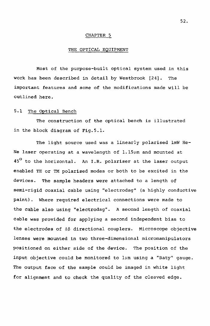
52.
CHAPTER 5
THE OPTICAL EQUIPMENT
Most of the purpose-built optical system used in this
work has been described in detail by Westbrook [24]. The
important features and some of the modifications made will be
outlined here.
5.1 The Optical Bench
The construction of the optical bench is illustrated
in the block diagram of Fig.S.l.
The light source used was a linearly polarised ImW He-
Ne laser operating at a wavelength of 1.15~m and mounted at450 to the horizontal. An I.R. polariser at the laser output
enabled TE or TM polarised modes or both to be excited in the
devices. The sample headers were attached to a length of
semi-rigid coaxial cable using "electrodag" (a highly conductive
paint). Where required electrical connections were made to
the cable also using "electrodag". A second length of coaxial
cable was provided for applying a second independent bias to
the electrodes of ~B directional couplers. Microscope objective
lenses were mounted in two three-dimensional micromanipulators
positioned on either side of the device. The position of the
input objective could be monitored to l~m using a "Baty" gauge.
The output face of the sample could be imaged in white light
for alignment and to check the quality of the cleaved edge.

II Q)
U goo00 Q)o :>
~o~
I I44
---,--' "-.,---
/
! 4 &I 0
~ -------- ~Q)E-!
1-+-1E --i>-- -i>-
10-1
·VI'd~oIII
sQ)a.0o00
_,.,_ .. 0.. ,... ~ 10-1~ Q)•.-1 +lo +l
1...---" _00 00 ~
"a.
" ~.~ ~,
"::<
, I 0," I
E-!... .."
..-+, ~, ,-., I "
I I,I >t, 10-1'0
10-1·0
:>+l•• .-1
E-! s::o
I,I)
10-1Q)s 00
:::itO~- N
LI'lQ)~z. ,..-IQ):r:
If)

53.
5.2 Waveguide Coupling
Light is coupled into and out of the waveguide by 'end-
fire' coupling. To avoid exciting radiation modes the
incident beam should match the profile of the guided mode to
be excited and be carefully aligned with the sample. Westbrook
shows that a 2.5~m diameter spot can be achieved by focussing
a laser beam with a x45 microscope objective provided that a
beam expander is positioned between this lens and the laser.
With this arrangement all the light emerges from the epitaxial
region. For many of the waveguides studied this spot was
sufficient to excite only guided modes. In some "weak" guides,_
however, it was found helpful to tailor the beam to further
match the elliptical shape of the guided modes. This was done
by using a narrow adjustable slit to diffract the expanded
beam. Unwanted slab modes could then be eliminated with care-
ful alignment.
5.3 The Detection System
In the main a detection system based on a Siemens XQll12
I.R. Vidicon tube installed in a LINK l09A camera was used.
The camera was positioned at the focal point of the output lens
and the Video-signal output displayed on a T.V. monitor.
Logic circuitry described by Westbrook [24] enabled
the information contained in a selected T.V. line to be displayed
on an oscilloscope. The circuitry counts line synchronising
pulses down from a pre-set line number and on reaching zero
applies a trigger pulse to the oscilloscope time base. If the
video signal is connected to the Y input of the oscilloscope

54.
the intensity information of the selected T.V. line can bedisplayed. Sampling the T.V. line with a box-car integratorallows a record of the oscilloscope display to be made on anX-y recorder.
The magnification of the output lens was '\,61and the_usable Vidicon target width 12.8mm. Each T.V. line scan lasts52~s, consequently each microsecond of video signal correspondsto (12.8 x 10⁻³/61 x 52) m i.e. ~4~mat the output waveguidecleave.
The light transfer characteristic or gamma of theVidicon tube was determined using a set of neutral densityfilters. The transmittances of these at 1.15~m were foundusing a spectrophotometer. The camera saturated when the laserwas focussed directly onto it with no sample present. Theneutral density filters were used in series, and in conjunctionwith several single-mode waveguides, to gauge the gamma of thecamera at lower light intensities. The electrical outputsignal was proportional to the input light intensity for cameravoltage settings up to the maximum used in making measurements.
A Roffin Ge photodiode (model 7462) was also used forlight intensity measurements. Using the neutral density filtersoutput current was shown to vary linearly with optical intensity.Laser output intensity measured using the photodiode remainedconstant with time after an initial warm-up period of about 30minutes.

55.
CHAPTER 6
RESULTS AND DISCUSSION
6.1 The Finite-Difference Method and Its ComparisonWith Some Other Techniques
This section presents and discusses the results of a
theoretical analysis of the rib waveguide structure shown in
Fig.6.l(a). Comparison is made between solutions obtained
using the effective index method, those given by the finite-
difference method and the results of Austin [68] who used a
variational method of solving the wave-equation developed at
the University of Glasgow and summarised by Macfadyen [69].
Values of effective refractive index (Neff)' for the
four TE modes supported by this structure as given by Austin
are :
N = 3.4061790
NI = 3.392070
N2 = 3.369115
N3 = 3.350042
The equivalent slab guide when solving using the effecti ve
index method is given in Fig.6.l(b) where NI = 3.357639 and
NIl = 3.411645. From the TM solutions for this structure the
effective refractive indices for the rib guide are :
N = 3.407891o
NI = 3.396829
N 2 :::l 3.379297
N3 = 3.359158

, I... a .,,I
fGaAs
+b c (a 1
n= 3·44 i iGaAIAsn = 3·35
'I... ---a--_..'
( b)
a= 311mb=1 ...mc.=O-4lJm
Fig.6.l Rib waveguide structure examined theoretically.

56.
For solution using the finite difference method the waveguide
was considered to be contained in a "box" of half-width 3wm
and depth 4wm. Increasing these dimensions did not alter
the calculated values of effective refractive index. If
refractive index values at mesh points falling on the boundary
between two regions are taken as the numerical average of the
values on either side of the boundary the following effective
refractive indices are found
N = 3.405947o
NI = 3.392044 x y O.lwm
N2 = 3.370022
N3 3.348966
and
N 3.406588o
NI 3.392964x Y = 0.05wrn
N2 3.371259
N3 3.350126
Closer agreement with analytical results was found for slab
waveguides using boundary refractive index values determined
from a consideration of stored energy and the continuity of
normal D and t~nGential E components at a dielectric boundary.
This leads to boundary refractive indices of :
(6 • 1)
for a boundary in the y direction, and
n = \/ 2n I 2 n 2 2 / (n1 2 +n 2 2 ) ( 6 .2)
for one in the x direction. The improvement in effective

57.
refractive index for a n/n+ slab waveguide can be seen in
for the structure of Fig.6.1(a).
Thus the numerical calculations all agree to within
0.001 «0.03%) for all modes. Effective refractive indices
obtained using the effective index method are in all cases
larger than those found using the finite-difference
technique. For the rectangular waveguide of Fig.2.4 a simple
argument can be used to show this is the case. The effective
index method overestimates the guiding by including the
"corner regions" twice giving transverse propagation constants
which are too small and a value of Neff which is too large.
This reasoning also explains why the results get worse for
higher-order modes and incidently close to cut-off [27].
If the product of field profiles in the x and y
directions from the effective index method is taken as an
initial guess to fields for use in the finite difference method
the correct solution is quickly iterated. The value of Neff

58.
obtained from the Rayleigh Quotient after one iteration is
too small because the guessed field profile is not the correct
one, being discontinuous at the rib walls (y = ±1.5~m).
However, because this value for Neff is too small and theeffective index method gives a value which is too large an
immediate error interval is specified for the correct result.
6.2 Attenuation in Dielectric Waveguides
Fig.6.2 presents published data on the attenuation
coefficient at a wavelength of 1.15~m as a function of n-type
doping for InP [70] and GaAs [71], [72] and shows InP to give
lower loss than similarly doped GaAs.
Fig.6.3 shows the calculated attenuation coefficient
(a) for the fundamental TE mode in an epitaxial layer with
Nd = 101Scm-3 on a more highly-doped substrate as a function
of guide thickness for both InP and GaAs. The calculation
of a from equation (2.10) was outlined in section 2.1.2. The
loss decreases slightly as substrate carrier concentration is
increased because the greater loss of the evanescent field in
the substrate is off-set by the better light confinement due
to a larger refractive index step. Attenuation increases
rapidly as the waveguide thickness is reduced to the cut-off
value as a result of optical fields extending further into
the substrate where loss is greater. Calculations using
metal claddings of gold and aluminium have also been
considered. Complex refractive indices of (0.34 - j6.4) for
gold and (1.5 - j12) for aluminium were extrapolated from
published data [74] as values at 1.15~m have not been reported.

a(cm-1)100.-------------------------------------~
10
1
//
//
/
//
/
/
/
//
//
//
//
//
//
//
//
//
/
InP
0·11-----------~--~--~----~----~--~~~10n
n-type carrier concentration (cm-3)
Fig.6.2 Attenuation coefficient at a wavelength of 1.15~m asa function of n-type doping.

2
4
3
1
\\\
\
\\- GaAs, n+ = 3 x 101 8cm-3
\
o 2 3Epitaxial layer thickness (um)
1
Fig.6.3 Variation of absorption coefficient with waveguidethicknes~ for the fundamental TE modes in InP andGaAs n/n slab wareguides. The_full curve for theGaAs guide with n = 3 x 1018cm 3 is given inFig.6.4.

59.
The large imaginary part of the refractive index of metals
reflects their high :~f(ecti vity. Fig.6.4 shows that for TEmodes attenuation for a metal-clad n/n+ waveguide is only
slightly higher than that for the equivalent unclad case, a
result of a small field in the vicinity of the metal.
For comparison purposes the variation of attenuation
coefficient with waveguide width was found for the GaAs/Gao.77
Alo.23AS waveguide discussed in section 6.2. The losses forthis waveguide, presented in Fig.6.S are due entirely to the
metal cladding with gold affording a reduction in loss when
compared to aluminium. The different behaviour of the two
slab waveguides is again governed by the refractive index
step at the guiding layer/substrate interface.
It is also possible to estimate loss in waveguides from
the field profiles calculated using the finite difference
method. As outlined in Appendix 9.7 the power attenuation
coefficient for the guide is given by
0. = __ ------ (6 • 3 )
The integrals can easily be evaluated in finite difference
form using the trapezoidal rule outlined in section 2.3.
Fig.6.6 shows a plot of a against epitaxial layer thickness+for an 8~m wide slot waveguide fabricated on n/n GaAs
(n = lOlsand l016cm-3, n+ '\1.2 x lOI8cm-3). Values are
slightly smaller than those for comparable slab waveguides
(Fig.6.3). This is thought to be because the strain-induced

15
a (em- 1 )
10
5
,\\\\\\\
_ - - AI CLAD
UNCLAD
\\\\\\\\4-.--™\\\",\\\\\\
\,,'\'\'\,
'\ .......~--~~, ," ............. ........ ................ ................ ..........._
-- --- --_
,\\\
o 1 2 3 4 5 6 1Epitaxial layer thickness (~m)
Fig.6.4 Variation of attenuation coefficient with waveguidethickness for+TE and TM modes in unclad and aluminium-clad GaAs n/n waveguides. In unclad guides a for TMmodes is slightly higher than for equivalent TE modes,the curve is omitted for clarity.

30
20
10
- -- AU CLAD-ALCLAD
FUNDAMENTALMODE
\,,,\\\,\,,\
FIRST MODE
o 4 52. 31Epitaxial layer thickness (~m)
Fig.6.5(a) Absorption coefficient variation with waveguidethickness for TE modes in a GaAs/GaAlAs waveguidewith gold and aluminium cover layers.

150
100
50
__ AU CLAD
--AL CLADFund.
,\\\\
Fund.' ,\\\.,
...."" ..... .... -
1 2 4 5oEpitaxial layer thickness (~m)
Fig.6.5(b) Absorption coefficient variation with waveguidethickness for TM modes in a GaAs/GaA1As waveguidewith gold and aluminium cover layers.

~:.1.
'"ex>
I -~ ~ ~U :1. m
'" '".... I ~0 ~ Ul 0....-i U Ul 4-1
III QJ~ Ul~ UlU QJ.,-l ~~ ~+l U
M .,-l~ ~Q) +l~m ~M QJ
~,. M m, m ....-i.,-lX ....-i
.. m m+l .,-l.,-l X0., m~ +l.,-l
o,QJ
N 4-1 .0",I
~ ~o o.,-lco+l ....UO~....-i:;j4-IX
mN
Ul....-im C'+*~ ~QJ- .,-l ..U QJ.,-l 'Cl4-1 .,-l4-I:;jQJb1o QJU :>
m~ ~0 I.,-l +l+l0m....-i:;j Ul~QJ QJ+l'Cl+l.,-l,::C~
N - ~
I ~~U b1.,-ld ~

60.
refractive index changes decrease into the crystal so causing
the fields to be guided more within the layer itself where
losses are lower. If this were so it would be expected that
losses due to the metal cover would become more significant,
as for GaAs/Gal Al As guides, and that by ignoring these the-x xfinite-difference method underestimates attenuation. It is
thought a reasonable approximation to ignore losses due to
the metal as most of the guided wave is confined under the
channel itself.
6.3 Guiding Mechanisms In Metal Clad Waveguides
Westbrook [24] pointed out that lateral waveguiding+he observed in epitaxial GaAs layers grown on n GaAs sub-
strates was not due to electro-optic effects [73] which, as
will become evident in section 6.5.1, would give different-guiding properties in the (011) and (011) crystallographic
directions and no guiding for TM polarised waves. Usingeffective index methods Westbrook also showed that inter-
diffusion at the metal-semiconductor interface [53] and small
variations in epitaxial thickness (caused for example by over-
etching with the KI/I2 gold etch) would lead to negligible
waveguiding.
The proposed slot waveguide structures show similarities
in design to the "metal-gap" waveguides of other workers [14],
[20] who proposed that lateral confinement is solely due to
a lower effective refractive index away from the slot arising
from the presence of the metal cladding alone. For a 2.5~m+thick GaAs epitaxial layer (n2 = 3.44) on an n GaAs substrate

61.
(n3 = 3.4375) effective indices calculated using (2.10), (2.24)
and the computer program of Appendix 9.2 are 3.437616 for an
air covering and 3.437600 for a gold covering. The effective
index difference (1.6 x 10⁻⁵) is not large enough to cause
the relatively strong lateral waveguiding observed.
Hamasaki and Nosu [34] reported an effective refractive
index difference of 4 x 10⁻⁴ for a "metal-gap" glass waveguide
with a 2~m thick guiding region of refractive index n2 = 1.57
and a substrate of refractive index n3 = 1.47. The larger
effective index step in this case is due to the greater
refractive index step at the n2/n3 interface which provides
greater confinement of the light within the guide and hence
in the vicinity of the metal. This was further studied by
calculating effective refractive indices for a GaAs waveguide
with a Gao.77Alo.23As confining layer which has a refractive
index of 3.35 [60]. This guide supports one TE slab mode for
GaAs thicknesses in the range 0.32 - 1.05~m. For a layer
thickness of 0.5~m the effective index difference betweenunclad and aluminium or gold clad regions is 5.7 x 10⁻³ and
for a thickness of l~m 1.8 x 10~3. The effect on optical
loss of the refractive index step between guiding layer and
substrate is discussed in section 6.1.2.
Thus, when discussing waveguides formed using different
impurity concentrations the effect of the metal on effective
refractive index may be ignored. However, when larger
refractive indices caused by material differences are used
this is no longer the case. When using the finite-difference
method of section 2.3 to model the experimental structures,

62.
therefore, only strain-induced refractive index changes and
those forming the original slab waveguide need be considered.
6.4 The Finite-Difference Method for Strain Waveguides
6.4.1 Slab waveguidesIn the development of the finite-difference method in
section 2.3 fields at the air/GaAs interface were equated to
zero (equation (2.31». The approximation can be made
because the dielectric slab waveguide is strongly asymmetric
Le.
and the normalised electric field strength at the nl/n2 inter-
face is practically zero. The assumption is tested here by
considering slab waveguides with the short-circuit condition
modelled analytically by allowing nl ~ o.Table 6.1 shows optical loss and Neff values
calculated from (2.24) and using finite difference methods
for an n/n+ GaAs slab waveguide (n+ ~1.2 x 10¹⁸). The
boundary condition of (6.1) gives a value of Neff closer to
the analytical one than using the arithmetic mean of the
refractive indices to either side.
6.4.2 Convergence of the finite-difference method
The number of iterations required for the finite-
difference calculations to converge to the required solution
depends on the number of mesh points and the accuracy of the
initial guess to the eigenvector. More iterations are
required for convergence when using a larger number of mesh
pOints as well as each individual iteration requiring more

63.
computer time. Table 6.2 presents values for the effective
indices NS and NA of the symmetric and asymmetric modes
calculated using the finite-difference technique for a l4~m
wide strain-induced waveguide with F = l200Nm-1 and different
mesh sizes. The refractive index variation with y at various
depths was given for this structure in Fig. 3.5. The
approximate number of iterations required for convergence to
six decimal places without the use of S.O.R. is also given
in Table 6.2. Although both NS and NA vary by ~2 x lO-~ on
halving the X mesh size the coupling length Lc calculated
using (9.55) changes only by ~O.lmm between X = O.25~m and
X = O.125~m.
In practice the use of S.O.R. reduces the number of
iterations required for convergence by a factor of about
three. This is illustrated in Fig.6.7 which shows calculated
effective index against number of iterations for the l4~m
slot structure described above for the case X = Y = O.25~m.
It can be seen from Fig.6.7 and Table 6.2 that the value of
the effective index increases as the field approximation
improves, either by having more mesh points or by continued
iteration. This is as predicted in Appendix 9.5.
6.5 GaAs Waveguides
6.5.1 Guiding at a remote metal edge
Fig.6.B shows the positional change £ calculatedr
from equation (3.26) for TE waves 1.5~m below a remote dis-
continuity such as that illustrated in Fig.3.3. 1.5~rn is
the approximate depth at which field strength of modes

oW0r-i
(!) Ul..c:oW S
:i.~~Or-i4-:
Ul ('(j
0 s:: ~Ln 0 (!)4-l(\J 0..-i ~ 0oW
('(j ::l UlH s:: (!)Cl) oM+J S::oWOM o H
0..-i ID4-1 oW 12.,
0 0 ('(j 0
· 0 H Hp:: (\J ~ ID P..
· (!) oW0
~0..-i tns::
U)lH OM
Z oro~" OMs:: ::l
0 0 tJ,
Ln0..-i IDoW :>0 ('(j
s:: ~::l4-1 ID.c('(j+J
Ul4-l
· 0 ('(j 0p:: 0· X s::0 (!) 0ro OMU) s::.wOM ::l.c r-i+J
Cl) 0
i":> Ul
0..-i
0oW ID0 U
Ln ('(j r::~ ID4-1 H(!) (!)H4-:
4-1 4-l4-1 (!) OMCl) :>'0
Z OM+J ID
0 OoW
0 Lf\ 0 Lf\ 0 Ln 0 Ln 0 t.n 0 t.n(!)oM
1+-1 r::£'<l (\J (\I 0 0 0- 0- co co I'- 4-1 OM<r <r <r ....1" <r <r ....:t £'<l r'0 £'<l r-n r'0 ~4-l....:t ....1" ....1 -cr ....:t <r -rr -cr ....1" ....:t ....:t <r. . . .IVl IVl l'n I'D I'D l'n I'[) l'n l'n I'n I'n l'n r-
1.0.ty\OMr>";

- ...
,III
1·5
r-I ', ,, "
I -,I ' ..........I
... ....... -,,I
--_-15 -10 -5 5 10 15
y (microns)--.... ..." .... .... ... ,
.... I'... ,... _
-1·5
FSSSSSSJ
Fig.6.S Positional change in Er for TE polarised waves ata depth of 1.5~m produced by a remote discontinuity(F = 360Nm-1)

64.
confined in the epitaxial layer is a maximum. In this
The waveguiding properties of the refractive index
changes produced by such a remote discontinuity were examined
using a lOO~m wide, O.6~m thick+, gold stripe. Single-mode
waveguiding was observed at each discontinuity for both TE
and TM polarisations. Fig.6.9 shows the TE polarised mode
observed experimentally together with the intensity profile
predicted by the finite-difference method.
The application of a reverse electrical bias to the
deposited metal Schottky electrode depletes the epitaxial
layer which quickly becomes punched-through. A large electric
field then fills the region under the Schottky diode and
fringing fields extend to the light-guiding region. The
electric field ~b is a solution of Poisson's equation:
Pd'l. E =--b £
(6 .4)
where Pd is the charge density.
For reverse bias voltages Vb greater than the punch-
through voltage the electric field is given to a good
approximation by
o > x > -h (6.5)
+All gold thicknesses quoted subsequently in this thesis arenominal values calculated from (4.1) to be consistent withWestbrook [24] and papers published on the present work. Asmentioned in section 4 film thicknesses estimated from (4.1)are ~1.5 times smaller than measured values. Measured filmthicknesses are used to calculate quoted figures for F.

Predicted by thefinite difference
method
- Experimental•
•
•
••
•
•• •
-5 0
.p'SSJ5 10 15
Fig.6.9 TE polarised mode profile found at the remotediscontinuity of Fig.6.8 and profile predictedby the finite-difference method.

65.
For TE waves the refractive index change produced through the
electro-optic effect by an electric field in the (100)
direction is [24] :
for 011 prOpagation~))
for 011 propagation)
(6.6)and
where r~l is the non-zero electro-optic coefficient in thereduced notation of Nye [56]. For GaAs r~l = 1.4 x 10⁻¹²mV-l
[25]. These is no electro-optic interaction with TM-like
modes [24].
As both TE and TM modes are guided by the strain-
induced refractive index changes the electro-optic interaction
with the TE waves may be measured. Equal amplitudes of each
mode were excited and the output focussed onto the Vidicon
camera. A crossed analyser was positioned between the sample
and camera and reverse bias applied to the Schottky barrier.
Fig.6.10 gives the resulting plot of intensity (normalised to
its maximum value) as a function of reverse bias for an edge
guide in a sample 4mm long. Total intensity was measured by
summing values taken from the oscilloscope for each T.V. line
on which the guided light showed. Relative intensity measure-
ments taken in this way gave agreement within ±5% with those
taken using the Ge photodiode.
If the field distributions of the TE and TM guided
modes are assumed the same the intensity varies as
(6.7)

1/1o1 • •
• •
• •
0·5
•
••
•o 10 20
Reverse bias Vb (volts)
Fig.6.lD The variation in the total near field intensity(TE and TM), caused by the interference of twoedge modes, as a function of bias voltage.

66.
where
(6.8)
and L is the sample length.
Using (6.7) to model the intensity distribution of
Fig.6.10 gives 6~as a function of Vb as presented in Fig.6.11.
The graph obtained is linear above z7V. The intercept voltage
Vb = 3.4V agrees with a calculated punch-through voltage of
3.9V for a 2.7~m epitaxial layer with a carrier concentration
Nd ~7 x 101~cm-3. The stripe direction was determined to be
in the (all) crystallographic direction from etch character-
istics (see section 4.1.4.1). Corresponding results were
found for edge guides running in the (all) direction.
6.5.2 Stripe waveguides
The device structure is illustrated in Fig.4.1 and was
studied in detail by Westbrook [24] who used stripe widths
between 17 and 29~m and gold thicknesses in the range 0.6 to1.Bum,
All devices exhibited transverse waveguiding for both
TE and TM polarisations, most with stripe widths between
about 17 and 30~rn in three separate regions of the cross-
section, others at the stripe edges only. Measurements were
made on two devices of Westbrook's (A6XA and A18YA) over a
period of 30 months. Fig.6.12 compares the guiding properties
of A18YA measured in November 1981 and by Westbrook in 1978.
It is clear that they have changed little. A summary of the
measurements made on this and other devices is given in
Table 6.3.

4
t:.!3 L
(radians)
3
2
1
,I
II, Reverse biasI
I (V)I
5 10 15 20 25oFig.G.ll Phase modulation characteristic obtained from
Fig.6.l0 using equation (6.7).

I,IIIII/
19781981
I\\\\\\\I
\
.....
\,\\,,\\\\,\ ,
.....' ... ..,.."
:\,\\\\\\\,\,\\\\\\
... -
\
\
-30 -20 20
IIII\,
-10 o 10
Fig.6.12 The three TM mode profiles of device A18YAmeasured in 1981 and by Westbrook [24] in 1978.

67.
The three guiding regions observed in the stripe devices
of width 17-30~m suggested that each of the three minima in
the ~£r profile of Fig.6.13 is capable of supporting a wave-
gUide mode. Westbrook analysed the guiding properties by
approximating the refractive-index profiles to ones for which
the wave equation can be solved analytically. He chose a
parabolic profile for the centre regions and l/cosh2 ones for
the edge regions. The experimental results he obtained showed
good agreement with his theoretical predictions.
To gain further insight into the validity of these approx-
imations the guiding properties of an edge waveguide (F = 360-1Nm ) were analysed using the l/cosh2 approximation, an
exponential one [26], [75] and a one-dimensional finite-
difference technique. Using the refractive index variation at
a depth of 2~m the intensity half-widths and effective
refractive indices of Table 6.4 were found. Effective indices
obtained using the finite-difference method at depths of 1.5~m
and 2.5~m are 3.440975 and 3.44064 respectively and corres-
ponding half-widths are 5~m and 6.3~m. For a full two-
dimensional analysis field profiles at each depth were in
precise agreement with the finite-difference values above and
a value of Neff = 3.43845 is obtained (this analysis includes
the substrate refractive index of 3.4375). Experimentally
determined half-widths were 7.6~m for a TE mode and 7.3~m for
a TM mode.
Finite-difference calculations for a 28~m stripe with
F = 360Nm-1 show light mainly guided in the edge region with
a secondary peak under the stripe centre having a maximum

Fig.6.l3
10
5
-20 -15 -10 -5 10 15 20
-5
-10
-15
5
Microns
The variation of E with y for TE polarised wavesrat a depth of 1.5~m produced beneath a 24~m widestripe (F = 360Nm-2)

68.
amplitude less than 20% of that in the edge mode. By artif-
icially forcing zero field "walls" at the stripe edges modes
with half-widths of ll~m and 12~m are found under a 27~m
stripe with F = 360Nm-1 and 1200Nm-1 respectively. The
parabolic profile approximation of Westbrook predicts a half-
width of lO.6~m for F = 360Nm-l•
In device lOFE80A6, with a lO~m stripe width, no central
guiding region was found. This is in agreement with strain-
induced refractive index changes since the central guiding
region vanishes for this stripe width as illustrated by the
perturbation in E for TE waves shown in Fig.6.14.r
It was shown in section 3.1 that by evaporating aluminium
onto a substrate pre-cooled using a Peltier cooling element
metal films with no measurable stress could be formed. A
stripe of width 12.7~m was formed in such a film using a 5 : 1orthophosphoric acid: acetic acid etch at 700C and a positive-
photoresist mask. No waveguiding was observed in this sample.
As the laser was coupled into slab modes a short distance to
either side of the stripe some bright and dark regions were
observed in the guiding layer. As the stripe was approached
the spacing of these increased until just the bright centre
region remained and finally this spread out and disappeared.
The origin of these regions is thought to be interference
between the incident light and that reflected from the region
under the stripe. This indicates some very slight change in
refractive index either due to the loading effect of the metal
on effective refractive index or to a small residual metal
stress not detectable by the method of section 3.1.

-15
10
5
-10 5 5 10 15
-5
-10
y (microns)
Fig.6.l4 The variation of Er with y for TE polarised wavesat a depth of 2~m_~roduced beneath a lO~m widestripe (F = 360Nm )

69.
The bright and dark interference bands were observed in
all the stripe samples examined but in general an edge wave-
guide was seen on approaching the stripe edge.
6.5.3 Channel (slot or metal-gap) waveguides - noveldirectional-coupler structures
The strain components and dielectric constant changes in
channel structures may be determined by superimposing those
found for each discontinuity considered on its own. Fig.6.lS
illustrates this at a depth of l.S~m for a l4~m wide slot with
F = l200Nm-1 and TE waves. Fig.6.l6 shows the positional
change in 6£ for a similar slot 7~m wide.r
Channels with widths between 6 and lO~m in O.6-2~m of
gold supported one TE and one TM mode directly under the
channel centre. Confinement improved as gold thickness was
increased. Fig.6.l7 shows the TE mode supported under a slot
lO~m wide, together with the profile of the fundamental mode
calculated using the finite-difference method (F = 600Nm-1).
The experimental intensity half-width of 9.6~m agrees
reasonably well with the predicted value of 7.S~m. The
effective refractive index calculated for the next mode in
this structure suggests that it is cut-off.
The intensity of the TE polarised light transmitted
through this device was measured using both the camera output
and the Ge photodiode for various sample lengths. To ensure
that the same amount of light was coupled into the guide the
device length was reduced by sequential cleaving at the output
side only and aligned by observing that the sample remained
in focus over all of the cross-section when viewed using white

5
".-//
~./
"../
/'
,"",I ,I ,
I "I
""
5 10 y (microns)
-5~77Z77/1 IZzzzzzzi
.'
Fig.6.lS Photoelastic contribution to dielectric constantat a depth of l.S~m for a l4~m slot withF = l200Nm-1• The dotted lines show thecontribution from each edge.

Fig.6.l6
-10
78
50
40
30
20
iO
-5
-10
-20
10 y (microns)5
Variation of E w i t.h y for TE polarised waves atra depth of l.5Mm produced beneath a 7Mmslot(F = l200Nm- 1 )

-20
Experimental --
-10•
• •
•
•
o
• Calculated
••
10 20Position(microns)
Fig.6.l7 Predicted and experimental profiles for the TEmode supported by a lO~m-wide channel in a l~mthick gold film.

70.
light from the back illuminator. Fig.6.lS gives the resulting
plot of loge (intensity) against sample length.
If the intensity varies as :
I = I exp(-aZ)o (6.9)
a value for the attenuation coefficient a of 1.7cm-1 is found
from the gradient of Fig.6.1S. This value is in good agreement
with the predictions made in section 6.2. The epitaxial layerthickness was 2.8~m and its carrier concentration 6-S x 1015cm-3.
Multiple reflections can be ignored as they contribute less
than 3% to the total output intensity even for the shortest
sample length used (2.5mm).
By extrapolating the straight line of Fig.6.1S to Z = 0
comparison can be made with the intensity of the incident
laser beam (found with a neutral density filter included in
the optical system). If 30% reflection is assumed at each
cleaved facet [76] an extra loss of ~10% is found. This can
be explained by imperfect matching between the exciting laser
beam and the guided- wave profile and the resulting excitation
of unwanted slab modes. Total insertion loss of a sample 2mm
long is therefore 5.5dB.
For a channel width of l5~m and a gold thickness of 2~m
two guiding regions were observed with a centre separation of
about l2~m. The two regions were observed simultaneously with
relative light intensities dependent upon the sample length.
The relative light intensity in the initially excited guide
followed closely a cos2 variation with sample length as in
Table 6.5. It follows from the discussion of Appendix 9.S

loge (intensi ty)
4· 5 ·Arbitraryunits
4
,"," ,
<, ,," -,
3·5
3,+-----~--__-+__--~~----~----;_-----r-----4--r_~o 2 5 6 81 3 4 7
Sample length (mm)
Fi~.6.l8 loge (intensity) as a function of sample lengthfor the waveguide described in Fig.6.l7.

71.
that the structure forms a novel, highly synchronous directionalcoupler. The coupling length, L , consistent with the experi-cmental results of Table 6.5 is (2.2 ±0.2)mm. Thus two synch-
ronous waveguides forming the directional coupler are the
respective edge guiding regions at each discontinuity forming
the channel. As the laser beam was scanned across the wave-
guide input slab guiding could be seen at first, then the
intensity pattern corresponding to exciting one guide, then
nothing, then the intensity pattern for excitation of the
second guide and finally slab guiding once more. The input
coupling lens moved about l2~m between excitation positions in
agreement with the guide separation measured from the near-
field intensity pattern.
Applying a bias to one electrode introduces a propagation
constant difference ~8 in one guide through the electro-optic
effect and so alters the amount of light in each guide at the
output facet. From the coupled-wave theory of Appendix 9.8
it is expected that the power in the initially excited guideobeys
(6.10)
where a2 = {C2 + (~f)2} and C is the coupling coefficient, C
= rr/2L. It was mentioned in section 4.1.2 that the totalcmetallised area of the device was reduced to give the con-
figuration of Fig.4.2. A guided mode could be excited at the
edge of each electrode remote from the channel and the electro-
optic interaction with the TE mode measured using the method
of section 6.5.1. This value of ~S can be used as an estimate

72.
of the phase change introduced between the two coupled TE waves
in the directional coupler on the application of bias to one
electrode. Equation (6.10) may then be used to estimate the
power in the initially excited guide as a function of bias;
giving the plot of Fig.6.l9 for a l5~m wide channel 1.9mm
long, assuming a coupling length of 2.4mm (which is within
the error limits of the Lc value measured by sequential cleaving).
This plot is consistent with the experimental results presentedin Fig.6.20.
The directional-coupler switch proposed by Kogelnik and
Schmidt [18], [19] in which the sign of ~S is reversed midway
along the sample length allows for electro-optic control of
the cross-over state (i.e. light at the device output is
confined to the non-excited or coupled guide) for a broad
range of sample lengths greater than Lc. This can only be
achieved for a sample length of (n+l)L where n is an integercfor normal biasing. In principle both switch states can be
achieved using a reversed ~B configuration but in practice
uniform biasing requires a lower value of ~B to achieve the
"straight through" state.
The device was realised by etching a 20~m gap in each
electrode perpendicular to the guiding channel. Bias voltage
may then be applied in such a way that the sign of ~B is
reversed along the sample length or kept the same. Extra loss
introduced by the gap was negligible.
Fig.6.21 presents experimental results on the transfer
of light with applied bias for a l5~m wide channel orientated
along the (011) crystallographic direction for a device with

~I/.)+>-'0>
0< 00-1- > iri• UJ
.....00
IJUJ-II- \.!)
-I 4"UJUJ000
-e- 0.0::-1
C'J t- < 0U 1:: 4"
II UJ Cl:W_JD__J UJ Z
\.!)~
0~
\.!)('J
D("\1
\.!)
0--.<,,_. Cl
0 0-. er:; ~ --0 L1"l -er !V1 (\1 0
C 0 0 0 c- O 0 0 Cl Cl
G

a
b
c
Fig.6.20 Near-field intensity ~attern at the output 0=a Lfiumwide channel 1.9mm long. At the vavecut deinput, the laser is focussed on the right-handgui0e (a) with zero bias light emerges mainlyfrom the unexcitec guide since sample length ~L .For biases of -2lV (b) and -30V (c) on the ri~h~-hand electrode the amount of light coupled to thenon-excited guide is reduced.

Q) . ...c:: c :>t.j.J 0 H.~ 0
J.O.j.J Q)
-> .j.J CIj..c::H.j.J
, '0 ~~:-> Q) 0"1 Q)
0< C} Ul·~ ~.'\1 r- • .-, .~~ CIj
• LW :-> '-...! r-f ,:: ~L.t; CD ;V; CIj 0IlL:...!
t :: S U'O._j f- H ClJ
._j • i'- Omr-fL:...!W· , '0 '::<3 0,
000 ::::.~ ~rv) 0 "r-I 0
• Cl:: _J L': Q) CIj U::\)f-<C • ,'\1 '0 S
L) ::L .~ H S11WO:: ~ 0 0L'._jO 0"1':: H_J w:Z 4-1
'0 ClJ... C) Q)..c::~.j.J .j.J
Cl .~ H,\.1 U ,:: ~
X .~ UL_~~ Q)./ c- Ulr-~ :>t ........
r-I Ul 0
.JC1 r-I CIj ~
CIj.~ ,::
• , Lfl .~..a .~.j.J .j.J.~ 4-1 ,::
L': ,:: 0 0:--'\J
.~ U
" ,::Q) 0 ClJ
Cl .c .~ .c,_.j.J .j.J .j.J
Cl U,:: ,:: ...~ ~r-I
If'.~ CIj
:>t +lr-e: .j.J CIj ,::
.r-i ClJ• Ul Ul S0 ,:: CIj.~
Q) HU: .j.J :>tClJ,:: .j.J 0;• L...-r--. .~ .~ X
Ul Q)Cl I .'J ClJ ,::.........
J.c Q) ClJ
<, .j.J .j.J H~, 0 ,:: CIj~ .~
C) 0- ~,.. r....Cl 0 Ul~ U' ..:r r'.I"j .'\1 Cl r-I .j.J
Cl C) Cl Cl 0 C__) Cl Cl Cl Cl +l CIj ,::0 .j.J.~r-I 0 0A-I .j.JA-I
r-IN
\D
0"1.~~

73.
electrode lengths 2.9mm (near the input) and 2.3mm (near the
output). Bias was applied in the normal ~S configuration and
unbiased electrodes were grounded. Fig.6.21 also gives a curve
calculated from (6.10). Biasing in the reverse ~S configur-
ation (Fig.6.22) gave an improved switching performance with
9% of the light emerging from the excited guide at a bias of
-20V. The best isolation obtained was 15dB in the crossed-
over state (3% of the intensity in the excited guide) using a
reverse ~S configuration with the bias on the first electrode
-15V and that on the second electrode -20V. The different
biases are required because of the unequal electrode lengths
enforced by a fabrication error. Families of curves taken
for this device by fixing the bias on the "input" electrode
at values between 0 and 30V and varying the bias on the
"output" electrode all showed good agreement with the pre-
dictions of coupled-wave theory.
A similar ~S directional-coupler switch was fabricatedwith a l4~m channel orientated along the (011) crystallo-
graphic direction. Electrode lengths for this device were
2.6 and 1.9mm. It was intended to make this device length
equal to 2L with a channel width of 15~m. Switching intocboth states was achieved as shown in Figs.6.23 and 6.24
although a rather large bias of -42V was required in the
normal ~S configuration to achieve 13dB isolation in the
"straight through" condition. Isolation of 16dB in the
crossed-over state (2.5% in the excited guide) was achieved
with the reversed ~S configuration.

000-['0
C\iC\iII II~(\J_J _J
l.U ll...!000['000
• t:.X 0::(\JI-f-
UUIIWWU_J_J_J W lJJ
o 0-
oco "-- -.0 Lfl ~ r<l (\J
o ci ci 0 0 c::i 0 0
o> o>
•
o
o.oLfl
I'-
0
Lfl
tn(\J
0
00cl
NN

.-lcO~0 S
~ s:: 0U) H+' <lJlH-' .c0 +J <lJ> :>
0< s:: HLrU-
0 0.-i ~• u.J
> III U-.:r m {/)
11 u.JcO {/)
_J I--
0.-i ~_J
III ..0 0
u.J u.J-cr ~
lIIaolH s::
-..00o 0.-i
.0:: _J - +J
~ I-- <C 0 s:: s::u~ 0 0
11WO::-cr
U_JO
0.-i U
_J u.J :z+JU Q)
IIIs::.c
- ~+Jf'Ii lH
cOH cO0 {/)+J[Vl cO s::<lJ
<lJ S'"Cl 0.-iIII
0.-i H- 0J ~ <lJOle.
Xra <lJ0
<lJ+J <lJ- 0J 0.-i $.-IU cOX<lJ {/)
- III +Js:: C
0.-i OM0
:>i A.0 +J :>;
oM $.-Itn . 0C s:: <lJ<lJO.c
-I+J OM +J
IIIC+J
0.-i cO <lJ0
$.-I :>...... '"Cl~cO<, I <lJ t:J"I ~,...... {/) 0.-i
0 OM 4-! ra0 0- W f'- -..0 lfI -, [Vl ('J 0
.-lC<lJcOOH0 0 0 0 0 0 0 ci 0 0 SUO-!
$.-I ~Oa::LOZ<JU
('V")
N
~.01
0.-irz.

~-r-! Ul
;JUl 0re! ;J
~ -r-! ~U) ..0 -r-!.... .jJ
0 4-l ~00
> 0 0
'0 o.0 U
~('\I .-
> 0 o (J)n -r-! ..c::II II • .jJ.jJ.-('\1
Ln U
....J ....J I"'-- ~ ..0J ;J.-I
l.U W4-l re!
LnOO 0 .jJ
~oo rO ~• 0:: 0:: • L1'l (J).- I- I-uu
Ul ElIiWW Ln re -r-!
u ....J....JI-l
_j l.U W ('\I OJ (J)C\J 'do.
-,-i ~0 ;J (J)0
tyI(J)
C\J 'd I-lLf' (J) re
.jJI"'-- -r-! UlU.jJ
• 0X ~(J) -r-!
Ln0
:>i~.-I
Ln .-lre! . :>i• C\J -r-! ~ I-l
I .jJ 0 0
0.r-! -r-! (J)
I· ~.jJ..c::
0-r-! cO .jJ
I-l~ ;J (J)
J .r-! tTl:>Ln -r-! re!
~4-l :3:I I"'-- .jJ ~
I .r-! 0 'd
·t 0 Ul U (J)~ .-I
Ln (J) en 0..jJ<J;JI Ln
~ 0-r-! "d U
I (J)0 I C\J 'd Ul El...... I (J) I-l 0<, I 0 Ul (J) I-l,.... -r-! :> 4-l
0 .-l OJ0 o- CD !'-- -o Ln -cr n 0J 0 re! I-l (J)
0. 0 e OJ
:>0 0 0 0 0 0 0 0 H
O..c:: ;JZ+l U
'<t'N
ID.ty\-r-!Ii.!

74.
When bias was applied in the normal 68 configuration to
the electrode pair near the excited waveguide some leakage of
light, from the directional coupler to the increased region of
refractive index under the biased electrode, was seen for
voltages greater than 25V. Thus as the light is transferred
back into the initially excited guide its field profile changes
not its maximum intensity. This is illustrated by the photo-
graphs of Fig.6.2S showing the transfer of light on application
of bias. Fig.6.2S(a), (b),(c) are for initial excitation of the
right-hand guide with bias applied to the left-hand electrode.
Fig.6.2S(d) shows similar information for initial excitation
of the left-hand guide with T.V. brightness controls and camera
gain adjusted to show more clearly the observed leakage under
the biased electrode.
For larger channel widths (>~20~m) it was found possible
to excite the asymmetric and symmetric modes forming the
directional-coupler separately. Directional-coupler action
could still be produced by careful beam alignment.
With less strain (film thickness <~l~m) a more general
illumination was seen when light was coupled into the slot.
In particular a single bright TE mode of half-width lO.6~m
was observed for central excitation in a channel of width l4~m,
F = 600Nm-1• Directional-coupler like action could be observed
with careful alignment of the input beam to either side of the
centre but was not as convincing as for larger film thicknesses.
No change in passive guiding properties has been noticed
in channel structures examined regularly over periods of up
to 18 months.

a
b
e
d
Fig.6.25 Transfer of light on application of bias inthe normal ~B confiquratior. for the devicedescribed in Fig.6.23. :n (a), (b), (c)the guide on the right-hand si~e is excitedat the input cleave and bias of (a) OV (b)-2SV and (c) -38V applied to the left-handelectrode. (d) shows similar informationfor initial excitation of the left-handguide and a bias of -33V. Note leakageunder the biased electroc1e.

75.
Experimentally determined values for the coupling length
for various slot widths and gold thicknesses are summarised
in Table 6.6. These values and the guiding properties of
channels with width between 14 and 20~m are now discussed in
the light of results from finite-difference calculations.
The asymmetric and symmetric TE mode profiles are found
by considering half the waveguide cross-section and applying
relevant boundary conditions at the symmetry plane as described
in section 2.3. Fig.6.26 shows the normalised TE amplitude
and intensity profiles at 1.5~m calculated for a l4~m slot
with F = l200Nm-1• From the amplitudes of the asymmetric and
symmetric modes output intensity patterns can be modelled.
Fig.6.27 shows the predicted intensity output profiles for
Z = 2nL , (2n-l)L , nL /2, 1.38L and 1.62L. From the super-c c c c cimposition of the computed symmetrical and asymmetrical normal
mode profiles (Fig.6.26(a) and (b» it was noted that a 25dB
isolation in each state, in agreement with the value reported
by Leonberger and Bozler [20], could be expected. Calculations
using eoupled-wave theory show that the experimental isolation
of better than l6dB in the crossed-over state is limited by
the unequal electrode lengths used. Du and Chen [77] show
that with equal bias in the reverse 68 configuration a cross-
talk level better than 20dB requires that ILI-L21 < 0.0198
(L1+L2).
From the calculated effective refractive indices NS and
NA of the symmetric and asymmetric modes the coupling length,
Le' for the directional coupler was found using (9.55).Fig.
6.28 shows the theoretical variation of Lc with F for a l4~m

1"' ,',r >, ,'\
I' <._,' "I I, \
: ', \I ,, I
, I,I,,,
I,,.• c t<'
,,,I,,
,I
1-'I 'I, \,
,I
..10
(microns)
oricrons
le,-10 ' ,0
II
,,\I,,\..
\, I,,I,,.,
,,-, e
-10 o(a) (b)
10(microns)
' .., ", .., ,,."I ,, ,,,,
,.-,,,,,I
,,IIIIIIIII,,,,I,,,
II
___ I
I,I
I,,I
,I
,,\
,,,, ,,\,I,II,I ,\ ,, I
, "I I, I\ ,, ,\ ,'11
".. ... ..,,I
,,,,II
,,,I,I\,,\ '-- ..
,,_,
'II •, ., ,
, II ,, ,I
I,,
,I,,\I\,\ ...'- - \
-10-10 o 10(microns)
oCd)(C)
Fig.6.26 Normalised wave profiles at a depth of 1.5~mcalculated for the fundamental symmetricaland asymmetrical modes in a l4~m wide slotdevice with F = l200Nm-1
(a) Amplitude of the symmetrical mode(b) Amplitude of the asymmetrical mode(c) Intensity of the symmetrical mode(d) Intensity of the asymmetrical mode
10(microns)
~10
crons)

2 2
.. .. ...... ...... .. U
.. ,.. .. H
~.. ,_
.. 0 at r--l
.. .. ...... I
.. .. ~.. N
.. .... .... .. II
lSI
0..Q
T
0
UH~N
II.... lSI
.... .. nj
.. ... r-0 CJ
H- 0.. 4-1
....(J) oQ) Hr--l N.r-i \04-10 ....-lHo,
Q)+J;:j
2o,+J
", ::l U0 H.. co.. ~ M+J.. .r-i r--l.. (J)
.. .. ~
.. Q) "Cl,... .. +J.. 0 cG
r: ~.. .- .. .Q- .r-i
.... '0 N
.. Q) <,
.. +J U
.. U H
.. .r-i ~'0Q)H U
0 0~
r I r-N
\0
tyI.r-i~

-...lez-L&..
00N
1.0
8N...
00Cl')-E
E"".s
Cl') N ... 0

76.
channel with a 2.S~m thick epitaxial layer together with experi-
mental values from Table 6.6. Small deviations in epitaxial
thickness in the experimental devices have been ignored. As
the confinement of each mode increases with F so the coupling
between the two guides is reduced and the coupling length
increased. The minimum observed in this curve may be explained
by imagining an effective index model as in section 2.2.2.
For a small refractive index difference NIl-NI Kogelnik [26]
shows that the effective refractive indices Ns and NA may be
written in terms of a normalised guide index b as :
NA ~ NI + bA (NIl-NI)S S
(6.11 )
where bAS
N"1. _ N 2
A IS=(N 2 N 2II- I
From (9.S5)
Lc(6 •12)
As F ~ 0 NI ~ NIl and Lc ~~. The increase in Lc as F ~ 00
described qualitatively above is also explained by this model
since F ~ 00 , b ~ band L ~~.SAcBy assuming a cos2(cz) variation in intensity in the
excited guide Fig.6.28 shows that with F nominally l200Nm-1
a 20% error in strain can be tolerated whilst still maintaining
a 90% cross-over condition at the nominal coupling length.
Using the thermal-stress model of section 3.1 this corresponds
to an operating temperature range of ±4SoC. In the directional-

77.
coupler of length 4.5mm described, however, light would switch
from being mainly in the coupled guide to the excited one for
a similar increase in F.
Fig.6.29 presents the theoretical variation of Lc with
slot width for F = 1200Nm-l, together with experimental data
from Table 6.6. In this case L increases as slot width iscincreased and coupling between the two guides is reduced.
Fig.6.30 illustrates the change of L with epitaxialcthickness. As the layer thickness is increased the field
maximum occurs deeper in the material where ~£ is smaller.r
Here lateral confinement is less and coupling lengths are
consequently reduced. The reduction of coupling length with
depth was confirmed by solving the wave-equation for NS and
NA for one-dimensional strain-induced refractive index profiles-1at various depths beneath a 14~m channel with F = 1200Nm .
It is interesting to note that Leonberger et al [78] found a
slight increase in coupling length with epitaxial layerthickness for their p+n-n+ channel-stop stripe guides. This
was confirmed by effective index calculations based on the
method of section 2.2.2.
Fig.6.31(a) (b) show intensity profiles of the symmetric
and asymmetric modes for a 14~m wide slot with F = 500Nm-l•
There is no central dip in the symmetric mode profile of Fig.
6.31(a) as for the F = 1200Nm-1 case of Fig.6.26. Excitation
of this symmetric mode (with a half-width of ~ll~m) would
explain the experimentally observed guiding for central
excitation in slots with metal thickness l~m or less.

N - -

oM
mc~u.-.c...
-EE:Y
cN -

0.-4 IIIc:
I 0... 1-1... -- 0-- ... .,.,f-- _- e--- III
..,,,...__--- ---- ... oU'0
-_ .....Q) .....III ...
0..... ,.......... ~ \
~ III 0 I
~e.c:,I 111
~ 0 0 tc: III,
>. 0) \III QI IIII .c:~ '0~o .-4 III- I c:
.QIIIIIl 0
.... )0)0 1-1
0'0 0.c:=' , .-4 .,.,f
"01II-iJ I ec: ..... ,"11:- ..... ..,
00. ----o-e --.... III --- - -_~ - _- 111-iJ ...... "Q) .. III '..~I =' ---- -- --et7' --->'Z Q) ----- --III J:J-8 g' .. 0
III 111 .,.,f _- ---"0__ - --II "0 _-- --III~~ _-,.
0 s ... 111~.c:o -_I
+11-1 ---- ----111 ..... 11-1 -- ---_QJ ) --~ t:7' ,....~c: \~O ..... \ 00 .....+I .-4~1n.-4 IC. ='
Q) In>'''0 Q) IIIoIJ ..... 1-I c.... ) 0!II Q) 0 ""Ce.-4 .-4 oIII ~ ..... , .....oIJ""~ I eC.-4 0 ,.... 1-1 . ,
III 0. en ... ..."0 a> ---QJ ~ >'''0 _- _, 111!II 0 ~ 0 _--..... 11-1 ..... 5..... In ..,-III In c: a> .., ..EQlQlen "'C+la> /ooc:.c: I 0 ta:z:e ......jJ ,
I\~ ,...
M ... ....-ID --- III-- It:7' --_ -..... -r&.. ...,
\
0~t

78.
Addition of equal amplitudes of each of these modes and squaring
the result gives the intensity distribution of Fig.6.31(c)
confirming the experimental observation that directional-
coupler like action could still be observed experimentally by
careful alignment of the exciting beam. Because the
directional-coupler behaviour is more distinct for larger F
this outweighs other advantages of working near the minimum
in the L IF curve of Fig.6.28.c
No propagating modes of higher order could be found in
the calculations for these structures.
After the metal film was removed from a slot-waveguide
sample there was no evidence for lateral waveguiding. In
another experiment a single-mode slot waveguide was formed
in a 2~m thick gold film and a further O.2~m of gold then
deposited over the whole surface to eliminate topographic
guiding effects. Waveguiding was still observed, although
the attenuation of the TM polarised mode in particular
appeared to increase slightly.
A 12.4~m "Nide slot waveguide produced in a "strain- free"
aluminium film using the method of section 4.1.3 showed no
lateral confinement for TE polarised waves. Slab modes were
seen for excitation on either side of the slab and some
interference effects similar to those described in section
6.5.2 for a "strain-free" stripe device. For TM polarised
waves no slab guiding was seen except for excitation
immediately under the ;:::hannelwhen evidence was seen for very
weak guiding.

79.
6.5.4 Single-mode channel waveguides in close proximity
Results for passive directional-coupler structures with
the geometry of Fig.4.3 are described in this section. The
aim of the present study is to show the importance of strain-
induced refractive index changes on device coupling length.
Fig.6.32 illustrates the variation of coupling length
with F for two 7~m wide channel guides separated by various
widths as calculated using the finite-difference technique.
Fig.6.33(a), (b) shows the predicted symmetric mode intensity
profiles for a l~m central electrode for F = l200Nm-1 and
300Nm-1 respectively. Comparing this Fig. with Fig.6.26 and
Fig.6.3l(a) shows the considerable difference to the profile
even such a narrow electrode makes. Table 6.7 presents
coupling lengths determined by the sequential cleaving method
of section 6.5.3 for directional-coupler structures with wave-
gUide widths ~8~m and separation 3-4~m. Coupling lengths
calculated from the finite-difference method, using measured
guide dimensions and a value of film stress determined from a
sample placed adjacent to the device during evaporation, are
shown for comparison.
In each case the separation of the guided modes was
about lS~m. For excitation directly under the central thin
electrode the device SSI with F ~lSONm-l (i.e. the smallest
film thickness) showed two peaks separated by ~12~m but of
lower intensity than for excitation of one or other guide.
Nothing was seen at the output for similar excitation in the
s~mples with larger values of F.

Le(nino
100r-------------~r_--------~---------- __/
10
/I /
I ', ,/
/ "I
',//'
F=1200Nm-1
/
///./
/
.I/
I /I ,
,/II /
/ ",,,
/
/
/
//
/
/
/
/ F=300 Nm-1
/
/
I
1~--_,-----+----~----+---~~--_+----~o 1 2 3 4 5 6Separation
I''!I
7
Fig.6.32 Variation of coupling length with edge separationand F for two 7~m wide channel guides.

...,/
........ '"_ ....-
,,II~- _""_,-_--_-----_-,-" "- .....
",I.......- --_ -.. -_
..._...... ..,
. ,,II
_",------~--------~--..... -_
,I
-....._-_ ----~-,,---_-__ -----_---_ ----- ---- -_ -_ - -_ -_ ..\
II

80.
In most cases the calculated coupling length agrees well
with those determined experimentally, the exception being
sample SS2. For this sample, however, examination under an
S.E.M. showed that the metal film thickness was greater than
that of the photoresist. In devices SS3 and SS4 therefore
multiple layers of photoresist were used for masking as
described in section 4.1.3. The other devices show a clear
trend of coupling length increasing with F indicating the
importance of strain. The increase between device SSI and
devices SS3 and SS4 is not, perhaps, as marked as might be
expected but is masked to a degree by a slightly smaller guide
separation arising from the thicker photoresist mask used.
Fig.6.34 shows the near-field intensity profiles recorded on
the X-Y plotter for various lengths of device SS3 and
excitation of each guide in turn.
In the small lengths of the samples remaining after the
sequential cleaving to determine coupling length no change in
guiding properties with time have been seen over a period of
up to 3 months.
No attempt was made to switch the devices using electro-
optically induced phase changes as such studies have already
been reported by Campbell et al [14] and Leonberger and
Bozler [20] who each quote coupling lengths which, using the
curves of Fig.6.32 suggest F ~ 300Nm-1• The metal films used
by these authors were electrodeposited so there is no thermal
component to film stress but it is feasible that the guiding
behaviour they observed was caused by refractive index changes
arising from an intrinsic film-stress component [44].

E'I!E
Ul an::3 co0•.-1 ""1-1 0rtj> •
=1-1 1-1o ::s ,II-I+J
II>t= ,
.-1-.-1 ,
.-I Q)rtj Q) "0 Q)+J"O •.-1 "0=-.-1 ::s •.-iQ) ::s tJ't ::s~tJ't tJ't•.-1 "0I-I.e:: , s:: 't1Q) 0 ~ rtj s::~rtj ..' .e:: rtj>< Q) -_ ... _ ..... .---- I .e::Q)II-! _------ +J I
.e:: +Jroo E t)) 4-lQ)
l~ -.-I Q)ro= E 1-1 r-I1-1 00-.-1 ~ 4-l 4-lO+J M _---- 0 0Q) rtj ,-'--I-I+J ~
= s::-.-I J:I '......_- ...... 0 0Ul 0 --- •.-1 •.-iQ) >< +J +J.-IQ) rtj rtj-roI +J +J11-1"0 -.-I '.-ie~ 0 0
>< ><~ Ii:! Ii:!('\")>ttl)+JtI)-.-IUlQ)s:: 0Q) •.-1 -+J>= Q)-.-Iro
roll-!.-10Q)-.-IUlII-I.e:: .. ......I+J ..__
I!I-It)) -----rtj= E ------ -~.Q)Q). Z r-I E
N.qt ~('\")
"\0 ns•tTl-roIr..

81.
6.5.5 Evaluation of 900 waveguidingInfra-red radiation from the laser was coupled into the
input waveguide by 'end-fire' coupling, using a x45 objectivelens in the usual manner. The small sample sizes meant that asimilar objective could not be brought physically close enoughto image the orthogonal output cleaved facet onto the Vidiconcamera. A long-working distance x20 microscope objective wastherefore used for this purpose. A xlO objective at the outputwas found to make preliminary alignment easier as it requireda smaller change in position to focus the guided light afterinitially imaging the waveguide with white light from the backilluminator.
The effectiveness of the reflection was first evaluatedby forming an etched edge on n/n+ GaAs material and cleavingin a position to dissect the "wall" formed. On subsequentexamination slab waveguiding was observed as far as the etchonly. In the vicinity of the exposed end of the edge noevidence of radiation into slab modes or other forms of losswas found, even using a high camera sensitivity.
Extra loss introduced by the reflection was estimatedby producing a straight waveguide section from an adjacentpiece of material using the same fabrication technique. Thelength of this waveguide was cleaved to match the total lengthof the two orthogonal guides in the bent structures. Lossmeasured in this way showed that for different devices between35 and 70% of the light was reflected into the second waveguideby the etched wall. Typical etch profiles are presented in

82.
Fig.6.35(a}, (b) and show some roughness of about 0.5~ inmagnitude. From an examination of waveguide structures underan S.E.M. (as for example in Fig.6.35(c» a qualitativerelationship between edge roughness near the point ofreflection and loss was found. The smoothness of the etchedwall is limited by the resolution of the optical photolitho-graphy used. Although the reflection technique has beensuccessfully demonstrated it is thought that reproducibilityand improvement of results will require better definition ofthe edge, perhaps using a combination of electron-beam litho-graphy and dry etching.
6.6 InP Devices
6.6.1 InP Schottky diodesThis section describes measurements to verify the work
of Wada [66], [67] on increased barrier height in Au/n-InPSchottky barriers incorporating an interfacial native oxide.Current-voltage (I/V) measurements were performed on 600~mdiameter circular diodes fabricated on epitaxial InP sliceswith carrier concentration 1 x 101Scm-3• Measurements weretaken either using a Tekronix 577 I-V curve tracer or anelectrometer (model Keithley 602) and in the dark as thecharacteristics were light-sensitive. Fig.6.36 shows a typicalforward-bias characteristic for an unoxidised device and adevice oxidised for lOs and subsequently annealed as describedin Chapter 4. Fig.6.37 shows the reverse-bias characteristicsfor the same devices.
The I/V results are analysed using the thermionic-emission

a
b
5IJm
c
Fig.6.35 Etch woll profiles Ca), Cb) and waveguidestructure (c) for I'ro~osed bent-waveguidestructure.

IF 102I
(A) I,,I,
I
103
UNOXIDISED
,II,
IIII
:~j.9.6.36 Forward I-V characteristics of unoxidised and~ox1d1sed Schottky barriers. Oxidation for lOswas followed by annealing at 250°C for 30 min.A = area

Ir 104 ~--------------------------------~
(A)
-710
UNOXIDISED
A=2.6X10⁻³ CM 2
1~1~--~~----~~--~--~~-4--~0·1 1 1M)
-810
-910
-10
10
100V r 'r \_'\j)
Fig.6.37 Reverse I-V characteristics for the sameSchottky barriers as in Fig.6.36.l\. == area

83.
model for a Schottky barrier given by Wada as
J J seV[exp( k T)-l]nr B
(6.13)
where the saturation current density
(6.14)
**A is the effective Richardson constant, for an effective mass* **m = 0.078 m , Ae
-2-28.4 Acm K ,kB is Boltzmann's constant,
V the applied voltage, and nr is an ideality factor which
accounts for departures from the simple thermionic-emission
model.
From the gradient of Fig.6.36 an ideality factor of 1.05
is obtained from (6.13) for both unoxidised and oxidised
barriers. Using (6.14) barrier heights of 0.46eV (unoxidised)
and 0.77eV (oxidised) are found from the current-axis inter-cepts. The reverse characteristics of Fig.6.37 show that due
to the oxidation leakage current is reduced considerably.
The results obtained show excellent agreement with those
of Wada who successfully applied a general theory of oxidised
Schottky barriers incorporating the effect of fixed charges
in the oxide layer to interpret his results.
A linear (capacitance C)-2/V characteristic taken on
another oxidised device confirms that the Schottky barrier
behaves normally but with an increased barrier height. The
technique is useful therefore for forming Schottky barrier
stripes for the waveguide structures described in Chapter 4.

84.
6.6.2 InP waveguides
6.6.2.1 Stripe structures
Schottky barrier stripe structures with various gold
thicknesses and stripe widths have been studied.
A 39~m wide stripe with a 2~ gold thickness showed two
very intense, well-confined- guiding regions one at each stripe
edge for both TE and TM polarisations. Further a broader, less-
intense guiding region could be excited directly under the
stripe centre for both polarisations. Fig.6.38 shows the three
TM polarised modes for this structure. The half-width
measured for the centre mode is l5~, those for the edge modes
6~.
Both TE and TM polarised modes are guided under the
Schottky barrier stripe at zero bias enabling the electro-optic
interaction with the TE waves to be measured using the technique
described in section 6.5.1. Fig.6.39 shows the resulting plot
of I<STE-BTM) IL = 6BL as a function of the bias voltage. Using(6.5) and (6.8) the non-zero electro-optic coefficient r41 ofInP was found to be (1.6 ± 0.4) x 10-12mV-1. This is in good
agreement with the value of 1.45 x 10⁻¹²mV-1 measured at l.06~m
by Tada and Suzuki [79J. The intercept on the voltage axis
agrees closely with that calculated as required to deplete
the epitaxial layer. It is larger than the intercept of Fig.
6.11 due to a thicker layer and a slightly higher carrier
concentration.
Stripes of width 27~ and gold thicknesses of 0.3,0.7
and 2~m also showed guiding at both stripe edges together with

20 urn
Fig.6.38 Experimental mode profiles for the three TMpolarised modes supported by the photo-elasticrefractive index changes from a 39~m wide goldstripe 2~ thick on n/n+ InP.

3
~BL(radians)
2
1
o 5 10 15 VbVolts
Fig.6.39 Phase modulation characteristic obtained fromthe interference of the TE and TM polarisedcentre guided modes of a 39~m wide gold stripeon n/n+ InP.

85.
less-intense but well-defined guiding under the stripe centre.
Figs. 6.40 and 6.41 are composite pictures of the three TM
polarised guided modes for the 2~m and 0.7~m gold thicknesses
respectively. The ease with which the guided modes could be
excited increased with gold thickness.
The results on stripe structures described so far may be
explained by a positional change in ~E similar to that shownr
for a similar stripe on GaAs in Fig.6.l3. The two edge guiding
regions only were observed in 16 and l8~m stripe devices with
2~m gold thicknesses and a 24~m stripe structure with a l~m
gold film. In these cases light input under the stripe was
expelled to either side probably because of the central
increase in refractive index being absent or too small to
support a guided mode.
A summary of the guiding properties of stripe waveguides
fabricated in InP is given in Table 6.8.
6.6.2.2 Channel structures
Channels less than 10~m wide showed single-mode wave-
guiding for both TE and TM polarised waves. Fig.6.42 gives
the guided mode profile for the TE mode beneath a 10~m wide
channel in a gold film 2~m thick. By observing the output
intensity for various sample lengths progressively reduced by
sequential cleaving at the output side the intensity attenuation
coefficient was measured as 1.2cm-1• This value is slightly
larger than expected from section 6.2 but a poor quality layer
(incorporating several "pin-holes") might account for this.
Channels of widths between l4~m and l8~m showed two

/\J \I \I \1 \I \r \IJJJIIII
. J
Ij
I
\\\\\
I\\\\
/ ...../ "-/
Fig.6.40 The three experimental TM modes for a 27~mwide gold stripe 2~m thick on n/n+ InP.

20 \-'''''
Fig.6.4l The three experimental TM mode profiles fora 27~m wide gold stripe O.7~m thick on n/n+InP.

10,((\.
Fig.6.42 Guided mode profile for the TE mode beneatha lO~m+wide channel in a gold film 2~m thickon n/n InP.

86.
guiding regions positioned under the channel itself. The two
regions were observed simultaneously with their relative
intensities dependent on the sample length. Fig.6.43(a), (b)
shows intensity profiles recorded on the X-Y plotter for a
2.lrnrnlength of a l5~m wide channel structure with a 2~m gold
film. At the input cleave light was coupled into the guide on
the right-hand side in Fig.6.43(a) and into that on the left-
hand side in Fi~.~.43(b). Fig.6.44 shows a similar profile
for a 2.6mm length of the same sample with the guide on the
left excited at the input cleave. The relative light intensity
in the initially excited guide plotted against sample length
followed closely a cos2 variation showing that, as for similar
GaAs structures, a highly synchronous directional coupler is
formed. A coupling length of (3.1 ± 0.4)mm consistent with the
cos2 intensity variation is larger than that of (2.2 ± 0.2)mm
for a similar channel in GaAs indicating confinement is tighter
in InP strain-induced waveguides. If the photo-elastic
coefficients are assumed the same in InP as for GaAs the
increase in confinement would be explained by a smaller value
of El and a larger value of v, calculated for InP from the
data of Neuberger [60] using the method of Kirkby et al [57],
and the subsequent increase in e and e from (3.14) andxx yy(3.15).
6.7 Strain-Induced Waveguiding With No Epitaxial Layer
It is apparent from the discussion of section 3.2 that
strain-induced refractive index changes decrease rapidly with
depth into the crystal as well as laterally. It is reasonable
to expect that some form of strain-induced waveguiding will be

E-W::iraN
'0ra Q)-Ws:: -...-I-...-I 0
:x:~ Q)Q)s:: Q)S::'Ora -...-I..r:: ;:::lI} o t:r>
.cQ)'O'0 s::-...-I ra
8:..c:
E-W::1.4-1Ln Q)~~4-1 ~0.0
..c:.w0' '0c Q)Q)-W
~-...-I0§ ~
~• Q)N'O
-...-Ira ;:::lt:r>
H0'04-1 s::raUJ..c:Q)~.w-...-I..c:4-It:r>
I~o -...-I .H 0:: Q)0. :>~ra~raQ).w-~
-...-I 0UJs::E-WQ) ~ ;:::l.w -...-I p,s:: 4-1 s::
-...-I -...-I-oQ) ~ Q)
..c:o..c:E-i t:r>-W
('V)
~~r»-,-j
~

Fig.6.44 TE intensity profile for a 2.6mm lengthof the guide described in Fig.6.43 withthe guide on the left excited at theinput cleave.

87.
present in a channel structure without the initial confinement
of the epitaxial layer and this is confirmed by finite-
difference calculations.
Experimentally, guiding was found in a short InP slot
device with a gold thickness of 2~m but confinement was poor
and there was much leakage of light into other parts of the
semiconductor. The finite-difference calculations suggest
that under an 8~m slot with F = l200Nm-1 most of the light
should be confined in the first lOf1m or so of the substrate
and under the slot. By using different box depths for these
calculations the guiding was shown not to be an artefact of
the imposed boundary conditions.

r-
_E ---+-1 ---!~ __;-+-...~---I-------I~ f--~---+-~_+-~-+-'-, I-~-:o .q<.q<.q<.q<.q<.q<.q<.........
I
m IcmQJEo
I -.-I If).j...lN
1]0.j...l-.-I~.::e
IC
lH 00-.-1
.j...l
'd mOr-!.c ;::1.j...l 0QJr-!:8 mo
rl rl rlm m m000-.-I -.., -.-I.j...l .j...l .j...l
>; >; :>-.r-! r-! r-!m m m~ I ~ ,§
I
cmQJ
! E
1(j) •EO..c:.j...l-.-I
l;cQJoCQJ~QJlHlH-.-ICl
o-.-I.j...llf)
(j)oc(j)~(j)lHlH-.-ICl
Q) QJ.j...l .j...l-.-I -.-IC C
f------+--N-f--r-!-+--O-+--O I :- - - : -i:1.0 1.0 1.0 1.0 If) If) If)
lH ~ ~ ~ ~ ~ ~ ~lH M M M M M M MQJ .q<.q<.q< ~.q< .q< .q<
Z •••
........E::1.
M M
I
If)
o
o m -- c
m
I"QJoCQJ~QJlHlH
!b
o o
I.1__
N
-_
o
I
m~olH
-oQJ
.j...lmr-!;:sor-!moxQJ-oC QJ-.-I 'd
-.-IQJ ;:s:> 0">
-.-I QJ.j...l :>o mm ~~lH.QQJ m~r-!
mQJ:>
-.-I.j...loQJlHlHQJ
-oCmmmor-!r-!mo-.-I.j...l
P..o
88.

Ulp..S::'"dor ~~I~I~I'
_H__ +--__ ~-_+_ - i---+----
Ho4-l
oH
I
. .o 0
!
oNN~~
1.0
----+-----~-+---~------~---
,::CZ
oNN~~
0'1 M M CON If) If) 1.0N N N N~ ~ ~ ~I~L~~~
I-----s---+-----+--lf)--I -- .L.::i If) N If) N N
Cl)
Z
o o 0 o o
I
L1")L1")
L1") NL1")
N~I~I
I
.o
.o
89.
Ul(l) S'"d::iO~Sri

0-[--1··· isU)I I:j_Q)........'0 co co co I-
·M ...-l ...-l ...-l ...-l~ ::! +1 +1 +1 +1Ob"l.~4J "...... .....~ 0 0 0 0U)oA.t
co...-l+1
I-...-l+1
I-...-l+1
oo o
...-l...-l+1
I I
coN
co l-N N
o...-l o...-l
N NN • • •...-l I- I- 0'1
o o
In
01
1
1
: I ~I
0'1 0'1, 0'1 CO IN N INN I~----4---~-ol ~+I---ro~--o~----...-l+-~~-+--~--~--+---
CO et) I- CO CO
.~ ~ ~ ~: I ~ ~ : :, ~ £ ~ £ ~ ~ :Q) :>t...-ll :>t c :>t:> ~ ~ 1 ~ ~ ~:> A.t ~ ~ ~ 19 19
Cl ~ -, ~ gl ~ ~ ~ g, ~ g ~ ~; ~ I- ~ ~ ~ 1~ 4; ----I ~ ---- ~ - ~ - ~ ---- N N ...-l ...-l
'-- __ --'- __ --L-i iii I _j
.o...-l
.C...-l
II
o• InCO CO
+loz
'0Q)+l
+l COO...-l +lZOO U) Z
.~
. .o 0
oo...-l/\
90.
~o

91.TABLE 6.4
:Method of calculation Neff t~(llm)2
Exponential approximation 3.44033 7.11/cosh2 approximation 3.44019 7.3One-dimensional finite difference 3.44077 6
'-.
Guiding Properties of an Edge Guide (F = 360Nm-1)
Analysed at Depth 211m by Various Methods.
TABLE 6.5
i
Sample Percentage of Light in co s? (Cz) i,Length excited guide at (L = 2.2mm) I
I(mm) Output Cleave (Experimental) c;I
---"12.1 <5 0.01 I3.4 rv50 0.575.6 35 0.437.6 40 0.439 95 0.98
-
Experimentally determined light intensity in the initiallyexcited guide for various lengths of a 151lm channel wave-
guide and proposed cos2 variation

T · \Ul
~~'1j -o '1j .jJ
s:: s:: s:: c O"IS::C1j C1j C1j H ",1 • 0:J 0 CV')
0 \.D co o 0.. Ul..jJ N L.{) ...., ...., 4-4 I ..c: C1js:: . · ...., .jJ",1Q) \.D \.D \.D \.D >.C1j b'>.Q
~....,.jJ C. Q) s:: C Q)ca
0 Ul ...., Ul Ul o ill .-1<]U b'> .Q b'> b'> E
"~ C1j "~ ",1
Io ",1 ill.-1
~ E-< ~ r... .jJ H .-1 C1j.-1 r- 0"1 0) 0..8
O)N Q) 0)...., 0).-1 .jJ 0., E HI0) Q) 0) . 0) .
!",1 X C1j 0
Cl)\.D Cl) Cl)\.D Cl)\.D ~ ill Cl)Z
---_ f-~-__l_
ItJ"l tJ"l
b'> s:: cc '1j ",1 '1j ",1
Io~ 0) :> 0) :>-o Ul C1j Ul C1jc C1j C1j Q) C1j C1j 0) '1j C1j
o~ o~ ..jJ .-1 0,1 .jJ .-1 I Q).jJ
\~ .Q C1j U .Q C1j U Ul C1j
'd '1j C1j'1j4-4 4-4
I.-1 4-4 .-1 o~
0 U o Q) C1j I o 0) C1j .QQ)H -o ",1 '1j ",1 '1j
'1j b'> o~ ..jJ b'> ",1 .jJ b'> 0,10 C :J I C s:: :J s:: C :J..c: o~ b'> 0) "~ b'> Q) ",1 b'>.jJ .jJ Q)
I:J .jJ Q) :J
I.jJ Q)
Q) .jJ :> 0' .jJ :> I 0' ..jJ :>:8 o~ C1j Q) o~ C1j 0) o~ C1j
~ ~ Cl) ~ ~ Cl) ~ ~
N I I·Lf) 0- \.D "<!' CV') "<!' 0"1
HU § . +1 . . . ·.-1 N N CV') "<!'
........ N·N- I- 0 0 0 0 0 0I 0 0 0 0 0 0
~ E N N N N N \.DZ ...., .-1 ...., ...., .-1........
(-"
..c:..jJ..jJ-O'1j E "" L.{) L.{) Lf) \.D
I
N.-10~ :::i. ...., .-1 ...., ...., .-1 NU)~ ........
i I I I I I
92.
.-1C1js::o
o~
.jJUillH
o~
Cl.jJ
o.-1Ul
Ul:Jo
o~
HC1j:> Ul
HH Q)0"'"4-40..
:JUl 0..c:u.jJr»C0).-1
b'>s::",1.-10..:JoU
.-1C1j.jJs::0)E
o~
HQ)0..X~

_------,-- _ ..- .__ .. --_~----~-
~§~
..r::+J co
'0 tJl ·aJ c co+J aJrtl~ N 0 I r-~ . N I::1 tJl ~ C' 1.0 1.0U s:: ·r-! ...-1 1.0rtl~U 0.,
::10U
-
~§
r-! ~rtl+J..r::S::+J r-! 1.0aJ tJlS c +1 Cl"..-i aJHr-! 1.0 I r-aJ . · 1.0p,tJl Lf"l 1.0 co~ s:: .r£l . ..-1 1.0
~P,::10U
-r~.....I 0 0 0 Lf"l
rx.. S Lf"l 0 Lf"l N~I r-!1.0 ~ r""J
- -----~.~--
aJr-!P.. r-! N r""J ~S U) U) U) U)
rtl U) U) U) U)U)
93.

00
~(j)(j)U)
~(j)(j)U)
s::(j) N(j) MU)
~ IJ~Tjo 0 olocOz z z Zn.
(j)Ul
I"-M
.oMI
1.0
co o
o
UlenQ)~~o.r-i..c:: ........+l E
:::t'O~Mot9
N N
Io
co.oM
~ Lf)• M
co
.---f-~
NM
N• I"-
0'\ M
r-.N
I1 1_ J
94 .

95.CHAPTER 7
CONCLUSIONS
It has been demonstrated that optical waveguides may
be produced in both GaAs and InP epitaxial layers through
the photo-elastic effect. Such waveguides have been exploited
to produce a novel directional-coupler structure for integrated
optics with the advantages of high phase synchronism and a
short coupling length (~2mm) without rigid tolerances on the
fabrication process. By applying reverse-bias in suitable
configurations one of these directional couplers could be
sVlitched to give either the straight-through or the crossed-
over state at the device output. The capacitance of each
electrode was ~2pF per mm. corresponding to a 3dB bandwidth
of 1.6GHz with a 50~ line system for a 2mm long coupler.
This bandwidth could be improved by reducing the electrode
width thereby lowering capacitance. However, to ensure
guiding properties under the channel are not affected by
strain-induced refractive index changes arising from the
remote metal edges, an electrode width of at least 15~m is
needed. The Schottky diode structure of Fig.4.2 can be used
as a microwave strip-line. Ono [80] proposed a modulator,
based on the novel directional coupler structure described I in
which a microwave modulation signal propagates along the line
together with the light wave. The proposed structure allows
for an increase in operation frequency above the limit
imposed by the time-constant of the diode.

96.
A new method of analysing electromagnetic wave propa-
gation in waveguides where refractive index may vary in both
directions of the cross-section but is constant in the
longitudinal direction has been developed. Using this method
of calculation, which is based on finite-difference techniques,
experimental results in GaAs have successfully been described
in terms of the strain-induced refractive index changes. The
importance of strain in directiona~couplerstructures formed
by having two "metal-gap" guides in close proximity has also
been demonstrated both experimentally and theoretically.
In InP epitaxial layers similar strain-induced wave-
guiding has been observed experimentally. Although refractive
index changes cannot be calculated the experimental results
indicate that these are slightly bigger than in GaAs, possibly
as a result of larger strains due to a smaller Young's modulus
and a larger Poisson's ratio in InP. By applying electrical
bias to a Schottky metal stripe under which a guided wave withequal amplitudes of the TE and TM polarised modes propagates
the non-zero electro-optic coefficient r41 of InP was
successfully measured. This was the second measurement of this
coefficient in the world and the first using this technique.
Strain-free devices have been fabricated by evaporating
aluminium films onto cooled substrates and confirm that the
dominant lateral-guiding mechanism is strain-induced refractive
index changes. This technique might be useful for eliminating
strain-effects in other devices incorporating evaporated films.
A proposed method for forming bends in waveguides by

97.
reflection off an etched vertical wall has been shown to be
practicable, although different masking and etching techniques,
possibly using electron beam lithography are required if the
negligible loss predicted theoretically is to be achieved.
The ease of fabrication of all these strain-induced
waveguides makes them ideal for producing other devices, for
example Y junctions and Mach Zehnder interferometers could be
made using strain-induced waveguides with suitable electrode
geometries. Further work is required to understand more fully
the nature of the stress in evaporated metal films. These
studies should include an examination of the film structure
during growth and on subsequent cooling.

98.
CHAPTER 8
REFERENCES
[1] I.G.A. Davies, A.R. Goodwin, P.A. Kirkby and R.F. Murison:"Semiconductor Light Sources", ElectricalCommunication (The Technical Journal of I.T.T.)~, 338, 1981.
[2] A.C. Carter :"Active Components for Long WavelengthFibre Optic Systems", Allen Clark Research Centre,(Plessey), Annual Review 1981 (page 48).
[3] J.E. Goell and R.D. Standley :"Sputtered Glass Waveguidefor Integrated Optical Circuits", Bell Syst. Tech.J.48, 3445, 1969.
[4] A.R. Billings :"Integrated Optics in Later GenerationOptical Communication Systems", Proc. IREE Aust.,137, 1979.
[5] S. Shimada :"Fully-Engineered and Non-Repeatered FibreOptic Inter-Office Transmission Systems", TechnicalDigest of 6th E.C.O.C. (York), 427, 1980.
[6] R. Bouillie, R. Auffret and G. Le Noane :"Tuileries-Philippe Auguste : The First Operational JunctionLine in France" Technical Digest of 7th E.C.O.C.(Copenhagen), 15.3, 1981.
[7] C.J. Lilly and D.R. Bissell :"Some initial Results andExperience of Operational Optical Fibre Systems inthe U.K.", Technical Digest of 7th E.C.O.C.(Copenhagen), 15.4, 1981.
[8] H.J.M. Otten :"Fibre-optic Communications", ElectronicComponents and Applications, 1, 87, 1981.
[9] D.H. Newman :"Devices for Fibre Systems", New Electronics,55, 1982.
[10] T. Kimura :"Single-mode Systems and Components for LongWavelengths", IEEE Trans. Circuits Syst. CAS-26,987, 1979.
[11] R.C. Alferness :"Guided-Wave Devices for Optical FibreCommunications", 1st European Conference onIntegrated Optics, 46, 1981.
[12] F.K. Reinhart, W.R. Sinclair, R.A. Logan :"SimpleHeterostructure As Gal As Phase Modulator withx -xSn02-Doped In203 Cladding Layer", Appl. Phys.Le t t. 29, 21, 1976.

99.
[13] M. Papuchon, Y. Combemale, X. Mathieu, D.B. Ostrowsky,L. Reiber, A.M. Roy, B. Sejourne and M. Werner:"Electrically Switched Optical Directional Coupler:Cobra", Appl. Phys. Lett., 'l:]_, 289, 1975.
[14] J.C. Campbell, F.A. Blum, D.W. Shaw and K.L. Lawley"GaAs Electro-optic Directional-Coupler Switch",Appl. Phys. Lett., ll, 202, 1975.
[15] A. Carenco, L. Menigaux, F. Alexandre, M. Abdalla andA. Brenac :"Directional-Coupler Switch in Molecular-Beam Epitaxy GaAs", App!. Phys. Lett., 2i, 755,1979.
[16] J.C. Shelton, F.K. Reinhart and R.A. Logan :"Rib WaveguideSwitches with M.O.S. Electro-optic Control forMonolithic Integrated Optics in GaAs-Al Gal As",x -xAppl. Opt., 12, 2548, 1978.
[17] F.J. L~o~b~rger, J.P. Donnelly and c.o. Bozler :"GaAsp n n Directional-Coupler Switch", Appl. Phys. Lett.,29,652,1976.
[18] H. Kogelnik and R.V. Schmidt :"Switched DirectionalCouplers with Alternating 6B", IEEE J. QuantumElectronics QE-12, 396, 1976.
[19] R.V. Schmidt and H. Kogelnik :"Electro-Optically SwitchedCoupler with Stepped 6B Reversal Using Ti-DiffusedLiNb03 Waveguides", App I. Phys. Lett., ~, 503, 1976.
[20] F.J. Leonberger and C.O. Bozler :"GaAs Directional-Coupler Switch with Stepped 6B Reversal", Appl.Phys. Lett., 2l, 223, 1977.
[21] G.E. Stillman, C.M. Wolfe, c.o. Bozler and J.A. Rossi:"Electroabsorption in GaAs and Its Application toWaveguide Detectors and Modulators", Appl. Phys.Le tt., ~ , 5 4 4, 1976.
[22] H. Sasaki and I. Anderson :"Theoretical and ExperimentalStudies on Active Y-Junctions in Optical Haveguides",IEEE J. Quantum Electronics, QE-14, 883, 1978.
[23] P.J.R. Laybourn and J. Lamb :"Integrated Optics: ATutorial Review", Radio and Electronic Engineer,g, 397, 1981.
[24] L.D. Westbrook :"Strain-Induced Optical Waveguiding inEpitaxial GaAs Layers", Ph.D. Thesis, University ofSheffield, 1979.
[25] E. Garmire :"Semiconductor Components for MonolithicApplications" in "Integrated Optics", ed. T. Tamir,Springer-Verlag, Second Edition 1979.

100.
[26] H. Kogelnik :"Theory of Dielectric Waveguides" in"Integrated Optics", ed. T. Tamir, Springer-Verlag,Second Edition 1979.
[27] J.E. Goell :"A Circular-Harmonic Computer Analysis ofDielectric Rectangular Waveguides", Bell Syst.Tech . J. ~, 2133, 1969.
[28] E.A.J. Marcatili :"Dielectric Rectangular Waveguide andDirectional Coupler for Integrated Optics", BellSyst. Tech. J. ~, 2071, 1969.
[29] R.M. Knox and P.P. Toulios :"Integrated Circuits for theMillimetre Through-Optical Frequency Range". Proc.MRI Symposium on Submillimetre Waves (ed. J. Fox),Polytechnic Press, Brooklyn, 1970.
[30] H. Furuta, H. Noda and A. Ihaya :"Novel Optical Have-guide for Integrated Optics", Appl. Opt. 13, 322,1974.
[31] Y. Yamamoto, T. Kamiya and H. Yanai :"PropagationCharacteristics of a Partially Metal-Clad OpticalGuide Metal-Clad Optical Strip Line", Appl. Opt.,_!i, 322, 1975.
[32] T. Itoh :"Inverted Strip Dielectric Waveguide forMillimetre-Wave Integrated Circuits", IEEE Trans.Microwave Theory and Techniques, MTT-24, 821, 1976.
[33] W. McLevige, T. Itoh and R.Mittra :"New HaveguideStructures for Millimetre-Wave and OpticalIntegrated Circuits", IEEE Trans. Microwave Theoryand Techniques, MTT-23, 788, 1975.
[34] J. Hamasaki and K. Nosu :"A Partially Meta1-Clad-Dielectric-Slab Waveguide for Integrated Optics",IEEE J. Quantum Electronics QE-IO, 822, 1974.
[35] J. Buus :"The Effective Index Method and Its Applicationto Semiconductor Lasers", IEEE J. QuantumElectronics, QE-18, 1083, 1982.
[36] J.K. Butler and J.B. Delaney :"A Rigorous Boundary ValueSolution For the Lateral Modes of Stripe GeometryInjection Lasers", IEEE J. Quantum Electronics QE-14,507, 1978.
[37] R.W. Hornbeck :"Numerical Methods", Quantum Publishers,1975.
[38] G. Forsythe and W.R. Wasow :"Finite-Difference MethodsFor Partial Differential Equations", J. Wiley andSons, 1959.

101.
[39] J.B. Davies and C.A. Muilwyk :"Numerical Solution ofUniform Hollow Waveguides With Boundaries ofArbitrary Shape", Proc. IEEE 113, 277, 1966.
[40] D.H. Sinnott: "The Computation of ~vaveguide Fields andCut-off Frequencies Using Finite DifferenceTechniques", Weapons Research Est., Australia,Technical Note PAD158, 1969.
[41] D.H. Sinnott, G.K. Cambrell, C. Carson and H.E. Green:"The Finite Difference Solution of MicrowaveCircuit Problems", IEEE Trans. Microwave Theoryand Techniques, MTT-17, 464, 1969.
[42] B.A. Carre :"The Determination of the Optimum AcceleratingFactor for Successive Over-Relaxation", Computer J,i, 73, 1961.
[43] D. Marcuse :"Light Transmission Optics", Van Nostrand,1972.
[44] R.W. Hoffman :"Mechanical Properties of Thin Fi Lms " ,in "Thin Films" American Society of Metals, 1964.
[45] J.D. Wilcock :"Stress in Thin Films", Ph.D. Thesis,Imperial College, University of London, 1967.
[46] R.M. Tennent :"Science Data Book", Oliver and Boyd, 1974.
[47] R. Feder and T. Light :"Precision Thermal ExpansionMeasurements of Semi-Insulating GaAs", J. Appl.Phys. 39, 4870, 1968.
[48] R.W. Hoffman :"The Mechanical Properties of Thin CondensedFilms", Phys. of Thin Films, i, 211, 1966.
[49] A. Brenner and S. Senderoff :"Calculation of Stress inElectrodeposits from the Curvature of a PlatedStrip", J. Res. Nat1. Bur. Std., 42,105, 1949.
[50] H.P. Murbach and H. Wilman :"The Origin of Stress inMetal Layers Condensed from the Vapour in HighVacuum", Proc. Phys. Soc., B66, 905, 1953.
[51] C.W. Haworth: Department of Metallurgy, University ofSheffield, Private Communication.
[52] C.A. Neugebauer :"Tensile Properties of Thin, EvaporatedGold Films", J. App1. Phy s ;, 11.,1096, 196.
[53] C.J. Madams, D.V. Morgan and M.J. Howes :"Out migrationof Gallium from Au-GaAs Interfaces", Elec. Lett.,11, 574, 1975.

102.
[54] A. Durelli, E. Phillips and C. Tsao :IIAnalysis of Stressand Strain", McGraw-Hill, 1958.
[55] E. Vol terra and J. Gaines :"Advanced Strength ofMaterials", Prentice-Hall, 1971.
[56] J.F. Nye :"Physical Properties of Crystals", Oxford, 1957.
[57] P.A. Kirkby, P.R. Selway and L.D. Westbrook :"Photo-elastic Waveguides and their Effect on Stripe-Geometry GaAs/Gal_xAlxAS Lasers", J. Appl. Phys.,50, 4567, 1979.
[58] R.W. Dixon :"Photoelastic Properties of Selected Materialsand Their Relevance for Applications to AcousticLight Modulators and Scanners", J. Appl. Phys., 38,5149, 1967. --
[59] F. Canal, M. Grimsditch and M. Cardona :"Piezobirefringencein GaP and InP", Solid State Comm., ~, 523, 1979.
[60] M. Neuberger :"Handbook of Electronic Materials Vol.2,III-V Semiconducting Compounds", Plenum, 1971.
[61] A. Feldman and D. Horowitz :"Dispersion of the Piezo-birefringence of GaAs", J. App1. Phys. 39,5597, 1968.
[62] A.C. Adams and B.R. Pruniaux :"Gallium Arsenide SurfaceFilm Evaluation by Ellipsometry and its Effect onSchottky Barriers", J. Electrochem. Soc., 120,408, 1973.
[63] E.A.J. Marcatili :"Bends in Optical Dielectric Guides",Bell Syst. Tech. J. ~, 2103, 1969.
[64] M. Otsubo, T. Oda, H. Kumabe and H. Miki :"PreferentialEtching of GaAs Through Photoresist Masks",J. Electrochem. Soc., 123, 676, 1976.
[65] S. Iida and K. Ito :"Selective Etching of Gallium ArsenideCrystals in H2S04-H202-H20 System", J. Electrochem.Soc., 118, 768, 1971.
[66] o. Wada :"Junctions, Barrier and Traps in InP", Ph.D.Thesis, University of Sheffield, 1979.
[67] o. h'ada and A. Majerfeld :"Low Leakage Nearly IdealSchottky Barriers to n-InP", Elect. Lett., !i,125, 1978.
[68] M.W. Austin: British Telecom Research Labs., MartleshamHeath. Private Communication.
[69] D.N. Macfadyen :"Components for Gallium ArsenideIntegrated Optics Fabricated by Wet ChemicalEtching", Ph.D. Thesis, University of Glasgow, 1980.

103.
[70] W.P. Dumke, t1.R. Lorenz and G.D. Pettit ;"Intra- andInterband Free-Carrier Absorption and theFundamental Absorption Edge in n-Type InP",Phys. Rev. B1, 4668, 1970.
[71] W.G. Spitzer and J.M. Whelan ;"Infrared Absorption andElectron Effictive Mass in n-Type GalliumArsenide", Phys. Rev. 114, 59, 1959.
[72] E.P. Rashevskeya and V.1. Fistul ;"Infra-red Absorptionof GaAs Doped with Group VI Impurities", Sov. Phys.Solid State, ~, 2849, 1968.
[73] C.F. Buhrer, L.R. Bloom and D.H. Baird ;"Electro-OpticLight Modulation with Cubic Crystals", Appl. Opt.3,839, 1963.
[74] D.E. Grayed. ;"American Institute of Physics Handbook",McGraw-Hill, 3rd Edition, 1972.
[75] E.M. Conwell ;"Modes in Optical Waveguides Formed byDiffusion", Appl. Phys. Lett., 23, 328, 1973.
[76] R.J. Elliott and A.F. Gibson :"An Introduction to SolidState Physics and its Applications", Macmillan, 1976.
[77] L.J. Du and C-L Chen ;"Stepped Switched OpticalDirectional Couplers with Unequal Section Lengths",SPIE, 176, 36, 1979.
[78] F.J. Leonberger, J.P. Donnelly and C.O. Bozler :"Wave-length Dependence of GaAs Directional Couplers andElectro-optic Switches", Appl. Opt., 17, 2250, 1978.
[79] K, Tada and N. Suzuki :"Linear Electro-optic Propertiesof InP", Jap. J. Appl. Phys., 1:2.,2295,1980.
[80] S. Ono: Internal Report, University of Sheffield,Department of Electronic & Electrical Engineering,1981.
[81] G. Stephenson :"Mathematical Methods for Science Students",Longman, 2nd Edition, 1973.
[82] H-G Unger :"Planar Optical Waveguides and Fibres",Clarendon Press, 1st Edition, 1977.

104.
CHAPTER 9
APPENDICES
9.1 Reflection of Plane Waves at Plane Interfaces
Consider a ray of light incident on the general boundary
between two regions with refractive indices nJ and n2 at an
angle 81 to the normal. Let E., Et and E be the electric1 r
field amplitudes of incident, transmitted and reflected rays
and H., Ht' H the corresponding magnetic field amplitudes.1 r
TE Polarisation
Matching E components :
(E. + E ) = Et1 r
(9 • 1)
Matching tangential H :
Ht cos82 (9 .2)
Also E.1 2lQ_=H. nJ1
Et D._Q_=Ht n2
n 0 =/G~
( 9. 3)
and( 9 • 4)
where

105.
From equations (9.2), (9.3) and (9.4)
n2 (E. + E )cos82l r
(9.5)From equation (9 • 1)
Hence Er
E.l
njcOS8j-n2COs82nzcos82+njcos8j (9.6)
Now
so cos82 (9.7)
ErE.l
( 9 • 8)
For total internal reflection at the interface njsin8j>n2equation (9.8) mav then be written as :
ErE.l
----------8 . I 2 . 262njcos +JJnj Sln j-n2
(9.9)
which is of the form
(a-jb/a+jb)
where tan ¢TE = b/a.
The phase shift is therefore 2¢TE where
(9.10)
"If n~ = -jn2 equation (9.9) becomes:
njcos8j -jjl+ nj2sin281E 11 112 )2r n2 (n
=E. njcos6j , nj2sin~ejl + j /1+
11 11
n 2 \/ (n2 )2
(9.11)

106.
and the new phase shift is 2¢TE where
(9.12)
TM Polarisation
Matching tangential H
H. + H = Ht1 r
(9.13)
Using equations (9.3) and (9.4) this gives
(9.14)
Matching tangential E
(9.15)
Eliminating Et from equations (9.14) and (9.15)
E rE.1
n2cos81-nlcos82= n2cos81+nlcos82
(9.16), 2
n2cos8J +!Il-(~) sin28Jn I n2
v
As in the TE case there is a phase shift 2¢ on totalTMinternal reflection where

107.
I 2 .22.:n 1 SIn e 1-n 2
nlCOSe1 (9.17)
If n,._ is purely imaginary (n;a, = -jn;,4") equation (9.16)
leads to
(n 2 ") 2 n 1 cos e 1 (9.18)
n 1 2 (n 2 " ) 2 +n 1 2 sin 2 e I
since the numerator becomes
-jn2~- COSel-nl

9.2 Computer Program for the Solution of the EigenvalueEquation
108.

PROGRAM( ITSI)INPUT l=CROOUTPUT 2=LPOTRACE 1ENDHASTER SLABSCOMPLEX CN(3),CGUESS,CMGUESS,CSOLN,CHSOLNCOMPLEX CEGAMMA,CFK,CMGAMMADIMENSION RK(3),DECUT(4),DMCUT(4)REAL MSOlNCOMMON UAVEL,PI,FK
5 PI=3.1415926510 READ(l ,15) CN15 FORMAT(2(2EO.O/),2EO.O)20 READ(l ,25) T,UAVEl2S FORMAT(EO.O/EO.O)30 READ( 1,35) NY35 FORMAT(Il)40 URITE(2,45) CN45 FORMAT(lH ,2(2Fl0.7,5X),2Fl0.7/1H50 URITE(2,55) T ,UAVEL,NY55 FORMAT(lH ,'SLAB THIC~NESS=",EI4.7/5511H ,'FREE SPACE UAVELENGTH=/,E14.715521H ,'MODE=',11)60 FK=2.0'PI/UAVEL65 CFK=CHPLX(FK,O.O)70 DO 80 J=1,375 RK(J)=REALICN(J)~CN(J»80 CONTINUE85 CALL EHODESIRKll),RK(2),RK(3),T,HODES)90 URITEI2,95) MODES95 FORMAT( lH ,'NO. TE MODES;;;',11)
100 DO 120 JK=l,4105 CALL ECUT iI~r:(1 i,RI\(2) ,RI:I3) , Jf(.DECUT (JI{))110 URITEI2,115) JK,DECUTIJf()115 FORMAT(IH ,'lE MODE ',11, CUT OFF UIDlH;;;',E14.7)120 CONTI NUE125 IFIT.LT.DECUTINY» GO TO 400130 CALL RBETAIRK(1),R~12),R~(J),T,NY,MODE5,ESOLN)135 CGUE5S=CHPLXIESOLN,O.0)140 CALL CNTEICN(I),CNI2),CNIJ),T,CGUESS,CSOLN)1 4 5 C EGA IiMA=CMP LX I 0 • ° , 1 • 0 ) *CS Q R T ( CN ( 2 ):ICN I 2 H C F 1-<*CF K - CS 0 L NI C 5 0 LI~ )150 URITE(2,155) NY,ESOLN,CSOLN,CEGAMMA155 FORMAT(lH ,'TE MODE /,11,' : '/1H ,'ESOLN=',E14.7,5X,1551'C50lN~',2E14.7/1H ,'GAMMA=',2EI4.7!lH ,'***,***.*t**t*t*,t***')160 CAL l F'l0 1 (F: f: ( 1 ),RI((2 ) , R f': ( 3 ) , ESOL N ,T )165 CALL MMODESCRf(l ),RK(2),RK(3',T,HDDMS)170 URITEI2,175) MDDMS175 FORMATllH ,"NO. TM MODES=',Il)180 DO 200 JMf(=1,4185 CAL L MC UT (R f( Cl) ,I;:f: C2) ,RK (3 ) , JM r( , DMCUT (J i1K ))190 URITEI2,19~) JMK,DMCU1(JM~)195 FOR MHTIl H " TM MOD [' ,I 1 , CUT OFF U I II TH= , E 14 .7 )200 CONTINUE210 IF(T.LT.DMCUTINY» GO TO 4002 2 0 CALL R B MTA (R1<I 1 ) , R f( ( 2 ) , RI: ( 3 ) , T ,N Y ,1,0 n11S , MSOL N )225 CMGUESS=CMPLXIMSDLN,O.O)230 CALL CNTM(CN(1),CN(2),CN(J),T,CMGUESS,CMSOLNJ235 CMGAMMA=CMPLX(O.O,l .O).CSQRT(CN(2)*CN(2)*CFK+CF~-CMSOLNtCMSOLN)240 URITE(2,245) NY,M50LN,CMSOLN,CMGAMMA245 FORMAT(lH ,'TM MODE ',11,' : '/lH ,'HSOLN~',E14.7,5X,2451'CMSOLN=',2EI4.7/1H ,'GAMMA=",2E14.7)2 5 5 CAL L f' L 01 (R f: I 1 ) , R f: ( 2 ) , F:f: ( 3 ) , MS 0 L N , T )260 GO TO 500400 URITE(2,405)405 FORHAT(lH ,'MODE CUT OFF')500 STOP
109.
END

SUBROUTINE EMODES(RK1,RK2,RK3,T2,NE2)COMMON UAVEL,PI,FK
CC THIS SUBROUTINE FINDS NO. TE MODESC
110.5 61 = 1.7 022=(RK2-RK3)~FK~FK
10 02=SORT(022)15 Pl=SORT( (RK2-RKl )*FK*FK-022)35 NE2=INT( (02*T2-ATAN( (GHPl )/02) )/PI+1.)50 RETURN
ENDSUBROUTINE ECUT iRKl ,Rf(2,RK3,NE2,D)COMMON UAVEL,PI,FK
5 61= 1.7 022=(RK2-RK3)*FK*FK
1002:;:SORT(022)1 5 P' = S o RT ( ( RK 2 - RK 1 ItF 1<~ F I{ - Q 2 2 )45 D=(ATANi (GHPl )/02)+FLOATiNE2-1 HF'I )/0265 RETURN
END
SUBROUTINE RBETA(RK1,RK2,RK3,T2,NX,NE2,GUESS)COMMON UAVEL,PI,FK
5 022=0.010 L=O15 IF(NX.GT.NE2) GO TO 110
CC THIS PART FINDS THE TE MODES BETWEEN 1 AND NE2C
110 (]2=iFLOAT(2*NX-ll~PIJi2.0'T2))-1.0E-}/T21150=SORTIRK2-RK3)'FK120 IF(0.LT.02) GO TO 170125 CALL FEIRK1,RK2,RK3,Q2,T2,Fl,F2)130 IFIF2.LT.O.O) GO TO 250140 OA=(FLOATIHX-l HPIIJT2150 !1B=!12160 60 TO 175170 OB=O172 OA=(FLOAl (NX-l )lPI )/12175 02=(OA+OB)!2.0177 L=L+l178 IF(L.GE.l00) GO TO 410180 IF(ABS«02-(l22)/Q2) .LE.l.0E-5) GO TO 40018 5 CAL L FE ( R f( 1,F:f; 2 , Rf(3 ,(J 2 ,T2 ,F1,F:2)190 IF(Fl.GE.0.O.AND.F2.LT.0.O) GO TO 230195 IF(Fl.LT.0.O.AND.F2.GE.0.0) GO TO 210200 IF«Fl-F2).LT.O.O) GO TO 230210 022=02215 OB=02220 GO TO 175230 022=Q2235 QA=02240 GO TO 175250 QA=Q2+2.0E-7JT2255 OB=(FLOAT(NX)~PI);T2260 IF(O.GE.OBI GO TO 175265 QB=O270 GO TO 175400 GUESS=02405 RETURN410 STOP
END

SUBROUTINE MNODES(RK1,RK2,RK3,T2,NE2)COMNON UAVEL,PI,FK
cC THIS SUBROUTINE FINDS NO. TM MODESC
111.
5 Gl=RK2/RKl7 022=(RK2-RK3)*FK*FK
10 Q2=SGRT(022)15 Pl=SORT«RK2-RK1)*FK*FK-022)35 NE2=INT( (02H2-ATAN( (GHPI )/G2) )/PI+l.)50 RETURN
ENDSUBROUTINE MCUT(RK1,RK2,RK3,NE2,D)COMMON UAVEL,PI,FK
5 Gl=RK2/RKl7 022=(RK2-RK3'*FK*FK
10 Q2=SORT(022)15 Pl=SORT«RK2-RK1)*FK*FK-022)45 D=(ATMH (GHPl liQ2 )+FLOAT(NE2-1 HPl )/0265 RETURN
END
SUBROUTINE RBMTA(RK1,RK2,RK3,T2,NX,NE2,GUESS)COMMON UAVEL,PI,FK
5 022=0.010 L=O15 IF(NX.GT.NE2) GO TO 110
CC THIS PART·FINDS THE TM NODES BETWEEN 1 AND NE2C
110 02= (FLOAT (2t NX-1 H F' 1/ (2 .01 T2 ))-1 .0E-7 /T 2115 Q=SQRTIRK2-RK3)*FK120 IF(Q.LT.02) GO TO 170125 CALL FM(RK1,RK2,RK3,02,T2,Fl,F21130 IF(F2.LT.O.O) GO TO 2501400A=(FLOAT(NX-l'*PI)/T2150 OB=G2160 GO TO 175170 OB=O172 QA~(FLOAT(NX-l)*PI)!T2175 G2=(OA+OB)/2.0177 L=L+l17B IF(L.GE.l00) GO TO 410180 IF(ABS«02-022)/Q2).LE.l.0E-S) GO TO 400185 CALL FM(RK1,RK2,RK3,Q2,T2,Fl,F21190 IF(Fl.GE.0.0.AND.F2.LT.0.O) GO TO 230195 IF(Fl.LT.0.0.AND.F2.GE.0.O) GO TO 210200 IF«Fl-F21.LT.0.O) GO TO 230210 Q22=02215 I1B=02220 GO TO 175230 022=02235 GA=02240 GO TO 175250 OA~02+2.0E-7/T2255 OB=(FLOAT(NXI*PI)!T2260 IF(O.GE.OB) GO TO 175265 GB=O270 GO TO 175400 GUESS=G2405 RETURN410 STOP
END

SUBROUTINE FE(R~:1 ,RK2,RK3,(12, T2,F1 ,F2)COMMON UAVEL,PI,FK
5 61=1.07 63=1.0
10 Pl=SORT«RK2-RK1)~FK~FK-02*02)15 P3=SORT«RK2-RK3)~FK'FK-Q2~Q2)35 F1=TAN(02*T2)40 F2=02*(Gl*Pl+G3*P3)J(02~02-Gl~G3*Pl*PJ)45 RETURN
ENDSUBROUTINE FM(RK1,RK2,RK3,02,T2,Fl,F2)COMMON UAVEL,PI,FK
5 61=RK2/RKI7 G3=RK2/RI<3
lOP 1 =S(1R T ( (R K 2 - RK 1 ):t F f( ;j; FI< - Q 2 oj; Q 2 )15 P3=SORT«RK2-RK3)tFK*FK-a2~02)35 Fl=TAN(02*T2)40 F2=02*(Gl~Pl+G3*P3)/(02*02-Gl*G3~P1*P3)45 RETURN
ENII
SUBROUTINE CNTMIRN1,RN2,RNJ,T2,GUESS,SOLN)COMPLEX RN1 ,RN2,RN3,GUESS,SOLN,P1 ,02,PJ,QQ2,FUNCT,DIFF,CFK,CT2COMPLEX CG1,CG3COMMON UAVEL,PI,FK
CC THIS SUBROUTINE SOLVES THE COMPLEX EIGENVALUE EQN. FOR TH MODESC
10 CFK=CMPLX(FK,O.OI12 CT2=CMPLX(T2,O.O)
cC (CFK,CT2 ARE FK,T2 IN COMPLEX NOTATION)c
30 SOLN=CHPLX(O.O,o.O)40 002=CMPLX(O.O,O.O)50 02=GUESS60 LN=l70 CG1=RN2*RN2/IRN1*RN1)75 CG3=RN2*RN2/IRN3*RN3)
1 0 0 P 1 =CS °RT ( C F ~(* CF I :, ( RN 2 oj; R N2 - RN i ·1; F: N 1 ) - Q 2 ;1; Q 2 )120 P3=CSQRT(CFK*CFK*(RN2*RN2-RN3*RN3)-Q2*a2)
C150 FUNCT=CSINIQ2*CT2)!CCOS(Q2*cr2)-Q2*(CGltP1+CG3~P3)J1501(Q2*02-CG1*P1*CG3*P3)
C170 DIFF=CT2/(CCOS(02*CT2)~CCOS(Q2~CT2»)-«a2tQ2-CG1*CG3*1701PltP3)t(CGltIPl-G2*02/Pl)+CG3*(P3-Q2*02/P3»-(Q2*(1702CG1*P1+CG3*P3»*(Q2*ICMPLX(2.0,O.0)+CGltCG3*(P1/P3+1 7 0 3 P 31 P 1 ) ) ) ) I ( ( a 2 ~.Q 2 - CG1H G3 .I. F' 11:F'3 H; ( a 2 * Q 2 - CGH CG3~ F' H F'3) )
C190 IF(CABS«02-[102)/Q2).LE.1.0E-9) GO TO 260200 IF(LN.GE.200) GO TO 270210 LN=LN+1212 URITE(2,213) Q2,FUNCT,DIFF213 FORMAT(!H ,3(3X,2EI4.7»220 002=02240 02=Q2-FUNCT/DIFF250 GO TO 100260 SOLN=Q2270 RETURN
END
112.

SUbi,:uUT 111i~ CI~ i 1:. .. i\l; i ,hrl,~, h Id, i _, (ciJL2:J, '::;iJLIC'
COMPLEX RN1,RN2,RN3,GUESS,SOLN,Pl ,Q2,P3,002,FUNCI,DIFF,CFK,CT2COMPLEX CG1,CG3COMMON UAVEL,PI,FK
CC THIS SUBROUTINE SOLVES THE COMPLEX EIGENVALUE EON. FOR IE MODESC
113.10 CFK=CMPLX(FK,O.O)12 CT2=CMPLX(T2,0.0)
CC (CFK,CT2 ARE FK,T2 IN COMPLEX NOTATION)C
30 SOLN=CMPLX(O.O,O.O)40 002=CMPLX(0.O,0.0)50 02=GUESS60 LN=l70 CG1=CMF'LX(1.0,O.0)75 CG3=CMF'LX(1.0,0.O)
100 P 1=CSQRT (CF r( t CF f(' ( RN 2·~RN 2-RN 1.~RN 1)-02·~Q 2 )120 F'3=CSORT(CFK~CFK~(RN2*RN2-RN3~RN3)-Q2*Q2)
C150 FUNCT=CSIN(Q2~CT2)iCCDS(Q2*CT2)-02~(CG1'PltCG3~P3)!1501(02~Q2-CG1~Pl~CGJ*P3)
C170 DIFF=CT2! (CCDS (Q2~CT2 HCCDS IQ2~CT2) )- ((02*Q2-CG HCGT~1701F'1*F'31*ICG1*(P1-Q2*02/P1 )+CG3*(P3-Q2*Q2/P3»-(Q2~(1702CG1*P1+CG3*P3)*(Q2*(CMPLX(2.0,O.0)+CG1*CG3~(Pl/P3+1703P 3/F' 1))))/ ((02tQ2-CG 1~CG3t F'HPJ H W2-Hl2-CG peG3 *P 1*F' J ) )
C190200210212213220240'J""'" ~I V260270
IF(CABS«Q2-QQ2)/Q2).LE.1.0E-9) GO TO 260IFILN.GE.200) GO TO 270LN=LN+lWRITE(2,213) Q2,FUNCT,DIFFFORHAT(1H .3(JX.2E14.7))002=0202=Q2-FUNCT/DIFFGO TO 100SOLN=02RETURNi=IJTISUBF:OUTlt~E F'LO[(Rl ,R2,R3,Q2,T2)DIMENSION A( I 01)COMMON UAVEL,PI,FKDATA BLANK,STAR,LINE!lH ,1H~,lHI/
2 F' 1 = 5 0 RT ( ( R2 - F:I )j. F f~,~F I< -ln~ Q :2 )3 P3=SQRT«R2-R])*F~tFK-Q2*02)4 Bi = I • 0 / S Q RT ( 1 • 0 + F' 1~ F' 1 " ( Q 2 Hl2 ) )5 URITE(2,10)
10 FORMAT(1H ,'X:Y',56X~"FIELD STRENGTH'15 X=-T220 IF(X.GE.O.O) GO TO 3525 FA=B1*EXPIP11X)30 GO TO 6035 IF(X.GE.T2) GO TO 5040 FA = B1 ·1 leo S ( fJ 2f X )+ ( F'1 / Q 2 )I S I I~ ((l2 H ) )45 GO TO 6050 IF(X.GE.(2.0*T2)) GO TO 1155 5 F A = B 1 ,.. ( COS I Cl2·~ T 2 ) + ( P i /Q 2 1 ·tSIN ( (] 2~·T 2 ) )i EX F' ( - F']' I X- T 2) )60 NA=NINT(FAt50.0)+5165 DO 75 J=1,1017G AiJ)=BLANI{75 CONTINUE80 A(NA)·=STAR85 A(51).::LINE90 URITE(2,100)X,A
100 FORMAT(lH ,E9.3,101A1)105 X=X+T2120.0110 GO TO 20115 RETURN
END

114.
9.3 Characteristic Equations for the Effective IndexAnalysis of Directional Couplers
For TM modes in the equivalent slab guides (Fig.2.7)
elementary solutions of Maxwell's equations are sought
describing waves that do not radiate away from the structure.
EXponential or hyperbolic functions are suitable in regions I
and III: sine or cosine functions in region II. Taking
advantage of symmetry, suitable mode profiles are:
y>{c+a)
H2{coS(q2 (y-c-a)) - Asinq2 (y-c-a)}
(c-a) < y <. (c+a)
(c-a) > y > (a-c)
H2 {COSq2 (y+c+a) + Asinq2 (y+c+a)} -c-a < y < a-c
HI exp Cp i (y+c+a)) y < -a-c.
PI, q2, P3, c 3nd a are as in section 2.2.2.
Asymmetric Mode
y > (a+c)
H2{coSq2 (y-c-a) - Asinq2 (y-c-a)} c-a <. y < a+c
c-a > y > a-c
-H2{COS~(y+c+a) + Asinq2 (y+c+a)} a-c > y > c-a
-HI exp{Pl (y+c+a)} y < -c-a
Matching Hand Ex zb_l_
N. 2~
(c-a) the characteristic equations (2.28) are derived.
ClH xay fields at y = (a+c) and x

115.
9.4 Finite-Difference Form of Partial Derivatives
Consider the following mesh points :
x = -h o h
From Taylor's Theorem 181]
(lcP (l2cjl(dx) 2cjl(x+dx) = ¢(x) + 3X (x)dx + 2! + .....(lx2
Thus
(9.19)
and8¢ Ih
(l2¢ h2¢C CPA - + I"2T +(lx ...
0 8x2 o .
Adding (9.19) and (9.20 )
82¢ ¢ +¢ -2¢B C A + h2D48x2 0 h2
(9.20)
(9.21 )
Where D4 is a combination of third-order partial derivatives
in the interval considered.

116.
9.S The Rayleigh Quotient
Multiplying the wave-equation for a trial field c/J(x,y)
by c/J(x,y)and integrating over the cross-section yields
rr{¢V2¢ + n2k2¢2 - N2k2¢2 }dS = 0) .
(9.22)
Replacing c/J by (¢+oc/J) and k2 by (k2+cSk2) and neglecting
second-order variations in ¢ gives
(9.23)
From Green's theorem:
and following the same arguments as in section 2.3.2.1 the
contour integral is zero for guided modes. So (9.23) becomes
(9.24)
(9.25)
Le. ok2 = 0
Orthonormality gives 00
\'/,
r=Oa 2r
00
(9.26)2' a 2
r
The S are such thatr

117.
It has been shown therefore that a variational expression for
the propagation constant S of a planar waveguide follows
from the wave-equation and is
If (~V2¢+ n2k2¢2)dS~2~) ?
IfQ2 dS
(9.27)
Equality holds if a = 0 for r > 0 i.e. if ¢ = ~o.r
(9.27) yields a lower bound for S2 which improves
as the trial function ~ approaches the actual mode distri-
bution. For ¢ = ~o the expression has a maximum value equal
to 62•
The improvement of the value of S2 as ¢ approaches
the actual mode distribution is illustrated by the results
of Fig.6.7.

118.
9.6 A Method for Find~the ODtimum Acceleration Factorfor S.O.R. (S ) and a Practical Scheme of ComputeroSolution
The problem of solving the wave-equation is reduced
by the finite difference operator to solving the matrix eigen-
value problem
A¢ = AcjJ (9.28)
for the smallest eigenvalue Ao and eigenvector CPo. If an
initial guess b. is made to the eigenvector an approximation1
w to Aa may be found from the Rayleigh Quotient as :
w =*b. Ab.1 1
*b. b.1 1
(9.29)
and a bi+l found from the relation
= Hb.1
where H is the S.O.R. matrix for solution of (A-w)b = O.
Sinnott 140] shows that the eigenvalues of the
matrix H converge to give b. = CPo and W = Aa. He also states1
that the optimum convergence to the required eigenvector is
attained when the largest subdominant eigenvalue A2 is a
double root of magnitude (S -1).o
S may be estimated from a value of A2 determinedo
whilst iterating with S < S as [42jo
So
2
2{ 1+ [1- 02+S-1) ]~2}_1A2S2
(9.30)
If a displacement vector r. defined as1
r. = b. - b. 11 1 1-

119.
is computed after a complete iteration then r41], r42]
> 2lim Ir·+ll
{ l }
I r. I, l
(9.31)
where Iri+ll is any norm of the vector ri+l.
The practical scheme used for solving waveguideproblems using S.O.R. is :
(1) Guess eigenvalue and eigenvector.
(2) Perform 5 iterations with S = 1 and then use the RayleighQuotient to improve the eigenvalue.
(3) Estimate \2 using the absolute values of the elements ofthe displacement vector
A norm of the root of the sum of the squares of b.l
elements has also been used successfully.
(4) Calculate S from (9.30) and reduce it slightly [41Jo
using the expression
Sm So
(2-S )o- --4- (9.32)
suggested by Carre r421.( 5) Set S = S , re-iterate 3 times and recalculate S .m 0
successive estimates of So differ by an amount 6Se suchIf
thatI /\ S I
e'U=-5) <
o0.05 (9.33)
then the value of S is deemed to be the correct one andono further estimate undertaken.

120.
(6) Proceed with iterations until convergence is obtained to
the accuracy required and then perform a few final sweeps
with S = 1 to smooth the field solution r 38] .
A feature was included in the computer program to avoid
attempting to take the square root of a negative number when
calculating S from (9.30).oThis occurs when A2 > 1 indicating
that S is too large and the solution is oscillating. The
difficulty was overcome by reducing S as in (9.32) to a
minimum value of one and then recalculating after subsequent
iterations.
All the features described are incorporated in the
following computer program for finding the symmetric mode in
a strain-induced slot waveguide.

100 REM PROG TO CALCUL~TE Rl ~~D FiND FIELDS110 U=3.14159120 PRINT'X STEP LENGTH MICRONS130 INPUT X140 PRINT 'Y STEP LENGTH MICRONS'150 INPUT Y160 X5=X170 Y5=YlBO PRINT 'INPUT FILM DEPTH(STEPS)'190 INPUT H200 PRINT 'BOX H~LF UIDTH STEPS B'21 0 I NF UT B220 PRINT 'BOX DEPTH ~ STEFS230 IfIF' U T H240 PRINT 'STLOT HALFUIDTH S STEPS:;50 I NF'lIT S
260 FRUIT 1'>270 INF'UT N2280 PRINT 'N3=290 INF'UT 113
300 PRINT 'INPUT 'U ~HIC~NESS ~ICRONS'310INF'UT
121.
350
F=60C·:tTV= .nE= 1200'JOD = 2 IF" ( 1 .. 'j ) ;' ( U 'E !
F'=XIi= 'r''fO=StF[I J M Ii ( 1 '::,0 • 1:5 'J 'FOR J=l TO 8Y = ( J - i ).1 F:FOR 1=1 TO H-iX=IctPGOSUfi 1510N ( I • J ) = Ii:' I ( 1 + N::: ~r ( • 0.' rE 1+ • 11 J rE: i )NEXT 1FOR l=H+l TO ':'-1X= I 'IF'GOSUB i:;10]
3603/0380390400410420430440450460470~80490500 N(I.Jl=N3·(1+~2 :'(.0~IE1'.113IE:1 \510 NEXT I52'J I=H530 GOSUB 15:j540 N ~H • J I -= .~~ -=' ._ i~ ~ t I • + ' r. -= .; iJ ~ I -,
: 50 riP T _'" 0" )
5005705:; 0 ~:= = -u.
J9':B::~1
PRINTI I; c' II T
. ~.- ~.~. - ,-• : ...,...... 'c ... _
650 G='J660B1=1670 Dll1 r, c. "_':'
6S0DIMEl (;S0.::0)670 FOR I = ~ 7:J H - ;7 0 0 F 0 ;:; J = .:' . c ',.;-10 UI.Ji='720 liEn "730 NEXT i

740 N=1i3730 h3=-1276082=1nOB7=F2780FoR1=OTOA790FORJ=OTOB800El (l,J)=E(I,J)810NEXTJ820NEXT I830D2=Dl840Dl=O8S0FOR 1=1 TO A-I860 FOR J=1 TO B870 E(O,J)=O890 E(A,J)=O890 S = E ( I + 1 ,J)+ E ( 1-1 ,J ) + (X /Y ) , 2 i ( E ( 1 , J + 1 )+ E ( I , J-1 ))900 ECI,JI=S/(2t( 1+(X/Y)-2)-~'2~X·2t(N(I.J)-2-N-2))
910ECl,J)=B2~E(],J)-IB2-1 )~El II,J)920 ECI,F+;)=0930 ECI,0)=EI1.2)
9 4 0 [I 1 = [11+ H 8 S ( E ' I • J ) I [ ; I • J ) - t: i (; . "i , tEl i I • J ) )950 I'EXT J96:) NEXT I970 P=F'+ i
980 Dl=SGRI[ll)990F5=F'5~11 000 F'8 = F' 8 + 11010 REM ROUOTIENT1 02 0 FOR I 0= 1 TO,; - 11030 FOR J=: TO B1040 GOSUB 1560105') C=C+[l1060 IIEXT~:1070 J=11080 GOSUB i ~,6ij1090 c=e+O/21100 NUT IlliO FOR 1=1 TO ,,-I1120 FOR J=2 TO B1130 F=EIl.JI '"1140 G=F+G1150 NEXT J1160 G=G+EI1,1 )':/:1170 NEXT I
1180N=saR(C/G)I'~~X)1190C=0120GG=O1210 iF F'5~50 ~HE~ 123012::0GO SUB 1:5"')1230IF P8<3 -HE~ 1:50124030 SUB 1 ~~'J1250 IF F' '0-2' TI1[i; , ."
1 260 GO TO ~ ~,:t,1~70f;:=11:80 F'~'1NT ti~ : ~i1 290 1F F' = 1 T H:::r; i:= 'J1 3 (0 (I 1 F F', ,J ;,~ E :; 1 .: 01310 GO 10 -~,_,1320 B2=1.,,;':;1330F7=E:21340 GO TO -0\'
1350 FRlrJT) .....',:'-=;.·~
122.
1360 F'~: ll~ T ,= "..1370 f'Rlrii :-1= .~1320 F'R 1 in H- :r11]00 f'R! til '- : t'

123.
1420 PRINT 'DO YOU UANT FIELD--TYPE Y OR N'1430 INPUT 1$1440 IF Zi=~N~THEN 15001450 1=61460 FOR J=l TO B1470 PRINT 'E(':I:J:')=':E(I,J)1480 NEXT J1500 END \b\O N -::.l)(.f'.'l.-t-lY ....'fc)"l.)I''l.
1520 M=(Xd2+(Y-YO)h2)A21530 El=D*«1-VJ*Xd2*«Y+YO)/N-(Y-YO)/M)-V*«Y+YO)A3/N-(Y-Y0)h3/M»1540 E2=D*«1-V)*«Y+YO)A3/N-(Y-YOJA3/H)-V*Xh2*CCY+YO)/N-CY-YO)/H»1550 RETURN1560 Q=E(I+l,J)+E(1-1,J)-2*E(I,J)+(X/Y)~2*(E(I,J+l)+E(I,J-l)-2*ECl!J))+(NCI,J)*K*XlA2*Ell,J)1570 (j:;:Q*EII,J)1580 RETURN1590F5=01 600 PRINT·'P = .' : F'1610PRINT'FACTOR=':B21 620 P R I NT·'N = .' : N1630RETURN1640Ll=Dl/D21650 Bl=B21660 P8=O1670B9=B71680IF B6=5 THEN18301690 IF«CL1+B1-1)A2)/CL1*B1*B1»)1 THEN 17501700 ii2=21(1+SQR(l-( (L1+Bl-1 )'·2/(LHB1*Bl»»1710B7=B2ii20 B2=B2-0.4*(2-B2)1730B5=(B7-B9)174060 TO 17801750PRINT '4007 OK FOR P=':P1760B2=B2-0.4*(2-B2)1765 IF B2(1 THEN 82=11770 RETURN1780 IF ABS(B5/(2-B7»(O.OS THEN 18001790RETURN1800B6=51810PRINT'4055 SATISFIED YHEN P=':P1820 PRINT'FACTOR=':B21830 RETURN

9.7 Loss in Waveguides
From Maxwell's equationaD
v x H = J + a~ = (cr+jw£)~
v x H = jw£ E- c-
where £ = (n-jk)2£oc
From the imaginary parts of (9.34) and (9.35)
o 2nk£o- =w
k oor = .2wn£o
The loss per unit volume is
where E is the maximum electric field amplitude and the
intensity from the time-averaged Poynting vector is
~ f E HdA)))
t. )where E 1 )= -H n 0 )
Writing I = Ioexp(-aZ)dII = -aZ
From (9.36) the power loss in distance dZ is
and using (9.37) and (9.39), (9.38) may be written as
124.
(9.34)
(9.35)
(9.36)
(9.37)
(9.38)
(9.39 )
(9.40)

125.
But w,ll1o£o = w/c = ko (9.41)
Hence et =2koJnkE
2dA(9.42)
JnE2dA

126.
9.8 Coupled Wave Theory of Directional-Couplers
Consider two waveguides (labelled a and b) whose
evanescent fields overlap and each of which would propagate
with normalised amplitude A satisfying the equation :
dAdZ = -j8A (9.43)
without the other waveguide present. Interaction between the
two modes of the waveguides couples the differential equations
for their mode amplitudes Aa and ~ so that :
~ = -j8 A -jCAdZ b--n a
))))))
(9.44)
where C is the coupling coefficient giving the extent of over-
lap of the modes.
Unger [82] shows that in the coupling region the two
modes of the uncoupled waveguides form two new modes propagating
independently with propagation constants
81 2 = (S,±a) (9.45),
8c1where = 2"(8a1+Bb1) (9.46)
2a2 = (fi81 +C 2 ) (9.47)
and fi811 (8al-8b1 ) (9.48)= 2"
It should be noted that fi8 = 2fi81• 8 ,Bb are the propagationa1 1constants of the waveguides a and b in the section of the wave-
guide considered. The extra subscript has been added because

127.
later the possibility of having a second section of waveguideis considered where the propagation constants for waves inguides a and bare Ba2 and Bb2 respectively. Bl is calledBS and B2 is called BA elsewhere in this thesis.
Combining the two modes given by (9.45) the generalsolution to (9.44) is :
Aa = AlexP(-jBIZ) + A2exp(-jB2Z)Bl-S S2-S
~ = ( cal) Alexp (-jSIZ) + cal
)))
A2exp(-jS2Z»
(9.49)
If at Z = 0 mode a is launched with unit power and mode b withno power then :
and the amplitudes in each waveguide mode along the couplingregion are determined using (9.49). In particular at Z = ~1
boB1 -j(3 21 )Aa (21 ) = (COs(Pl-j s Lno • ) e c )
et )) (9.50)
and -j(3 ~1 )
~(2d (_ .if sin<Pl) c )= eet
where <PI= etR-l.
For phase synchronism between both coupled modes boB1= 0and from (9.50) the power Pa in the excited guide is :
Pa = cos2 C~1 (9.51)
while it transfers the power
(9.52)

128.
All the power incident in mode a transfers to mode b at
distances :
z = (P+~)7fC P = 0,1,2 •.• (9.53)
The coupling length L is the shortest length for completecpower transfer between phase synchronous modes and is from
(9.53) :
Lcrr= 2C (9.54)
From (9.47) and (9.48)
(9.55)
In devices studied ~Bl is introduced by the applied bias. In
order to model directional-coupler structures having a reversed
~B electrode configuration consider a second region of the
guide of length L2 with a ~Bl of the same magnitude but of
reversed sign.
In this region 2
)))))
(9.56)
where now
(9.57)
Le.
and
and Z2 is measured from the front of the second section.

129.
As the sign of llSl is reversed
Sal = Sb2Sbl = Sa2
}
so SI Sa2 = llSl + a,}= llSlS2 - Sa2 - a,
(9.58)
(9.59)
Thus from (9.49), (9.50) and (9.59) :
Al 1+A2 1 'llSl )A (0) = = COS<Pl- ~ sin<pla2 a, ))
~2 (0) = (llS 1+a,) All+(llS~-a,)A2l )C )
'C )= -E sin<Pl )a,
)
(9.60)
Solving for All and A2l and putting Z2 = ~2 and <P2 = a,~2 yields:
))))) (9.61)
-jSc~2~sin<Plsin<P2+jsin(<Pl+<P2)]e )
*Pa(~2) = A (_Q,2)A (~2) )a2 a2)
1 2 )= [COS<PlCOS<P2+ - (llSi ._C2) sin<p 1sin<p2] 2 )a,2 )2
llSl sin2(<P2-<Pl))
+-- ) (9.62)a,2 ))
* )Pb(~2) = ~2 (~2)~2 (~2))
2 )
= 4C2llSl sin2<plsin2<p2 + C2 sin2 (<Pl+<P2) )a,2 a,2 )
N.B. P + Pb = l.a

130.
In a similar manner expressions may be derived for thepower in each guide at the output of a device with moresections or with the magnitude of 6S1 different for eachelectrode pair.


![1060 nm GaAs VCSELs for Extended Reach Optical ... · 1060 nm GaAs VCSELs for Extended Reach Optical Interconnects in Data Centers Ewa Simpanen ... standards for 500 m and above [12]](https://img.dokumen.tips/doc/110x75/5e499564235f120ea07cdf96/1060-nm-gaas-vcsels-for-extended-reach-optical-1060-nm-gaas-vcsels-for-extended.jpg)


![Optical characterization of type-I to type-II band alignment … · 2017-11-09 · GaAs/AlGaAs material system [2]. To date, many GaAs/ AlGaAs nanostructures, in particular QDs and](https://img.dokumen.tips/doc/110x75/5e99ea94c8c26a550d1cbb00/optical-characterization-of-type-i-to-type-ii-band-alignment-2017-11-09-gaasalgaas.jpg)