Embed Size (px)
Citation preview

Ecole nationale supérieure de physique, électronique, matériaux Phelma Bât. Grenoble INP - Minatec 3 Parvis Louis Néel - CS 50257 F-38016 Grenoble Cedex 01 Tél +33 (0)4 56 52 91 00 Fax +33 (0)4 56 52 91 03 http://phelma.grenoble-inp.fr
Théophile DUBREUIL
Nanotech Master 2020
CEA Grenoble
LETI, DCOS, SCME, LICL 17 Avenue des Martyrs, 38000 Grenoble, France
Innovative 3D Technology of a nonvolatile memory cell for In-Memory-Computing
from 24/02/20 to 28/08/20
Confidentiality : no
Under the supervision of :
- Company supervisor : Sylvain BARRAUD, [email protected]
Present at the defense : yes
- Phelma Tutor : Panagiota MORFOULI, [email protected]

Glossary
Abbreviation Signification Definition
NWFET Nanowire Field Effect Transistor
Novel type of transistor device with excellent electrostatic control
RRAM Resistive Random-Access Memory
Non-volatile memory devices based on reversible resistance change
1T1R One transistor one resistor Memory cell architecture where each memristor cell is paired with a transistor which plays the role of a selector
FinFET Fin-based Field Effect Transistor
Type of transistor where the channel is a vertical thin surrounded by the gate on three sides
BEOL Back End Of the Line Adjective qualifying a fabrication technique where a wafer upper metallic layers are used for device fabrication
OxRam Oxide-based Random-Access Memory
Type of memristor in which the reversible resistance change is caused by the creation/annealing of an oxygen vacancy filament in a thin oxide layer
IoT Internet of Things New networking type in which many different connected objects interact with each other
IMC In-Memory-Computing New computing paradigm where some of the data processing task is directly done in the memory
LRS Low Resistive State Lower stable resistance state in RRAM functioning (by opposition to HRS)
HRS High Resistive State Higher stable resistance state in RRAM functioning (by opposition to LRS)
GAA Gate-All-Around MOSFET design where the gate is enrobing the transistor channel on all sides yielding good electrostatic control
IT Information technologies Technological field where computers are used to store, transmit and manipulate data
TEM Transmission Electron Microscopy
Microscopy technique relying on electron transmission through very thin samples allowing sub-nm definition

EDS Energy Dispersive X-ray Spectroscopy
Spectroscopy technique based on X-ray diffraction used for chemical / elemental characterization
DIBL Drain-Induced Band Lowering
Short-channel effect in MOSFET associated with a reduction of the threshold voltage for higher drain voltages
DRAM Dynamic Random-Access Memory
Volatile memory type in which memory cells contain transistors coupled with small capacitors
Flash Flash Memory Non-volatile memory type where cells can be electrically erased and reprogrammed thanks to floating-gate transistors
NAND NAND Flash memory type where floating-gate transistors are connected in series
NOR NOR Flash memory type where floating-gate transistors are all connected to the ground
MIM Metal Insulator Metal (stack) Stack of materials that constitute the active part and the electrodes of RRAM memory cells
SET SET Regular transition from HRS to LRS in a RRAM cell
RESET RESET Regular transition from LRS to HRS in a RRAM cell
Forming Forming One-time operation of RRAM where the cell goes from its pristine state to LRS (first operation)
IC, ICC Compliance current Maximum current that can flow through a RRAM cell during the SET
Vresetstop, Vreset Reset voltage Maximum absolute voltage attained during RRAM cell RESET operation
MW Memory Window Resistance difference between RRAM LRS and HRS extremum states, the higher the MW the higher the RRAM performance
IsatN Normalized saturation current
Saturation current of MOSFETs normalized by the transistor gate width
Vt Threshold voltage Threshold voltage of MOSFETs
RMG Replacement Metal Gate Gate-last fabrication technique where the transistor metallic gate is deposited during the last process flow steps
SL Scouting Logic Novel In-Memory-Computing technique based on parallel reading

Table of contents
I) Introduction: .................................................................................................................................... 1
I)1) The My-CUBE project .................................................................................................................... 1
I)2) NWFET and RRAM characterization .............................................................................................. 3
II) Work Environment .............................................................................................................................. 5
II)1) CEA-LETI/DCOS/LICL ..................................................................................................................... 5
II)2) Cleanroom facilities ..................................................................................................................... 6
II)3) Characterization platform ............................................................................................................ 6
III) State of the art ................................................................................................................................... 6
III)1) Literature review ......................................................................................................................... 6
III)1)a) NWFET operation and electrical properties ........................................................................ 6
III)1)b) RRAM operation, materials and electrical properties ......................................................... 9
III)1)c) 1T1R Memory cells structure, architecture and My-CUBE memory pillar ......................... 16
III)1)d) Memristors-based logic functions : Scouting Logic ........................................................... 17
III)2) Internship objectives ................................................................................................................. 19
III)2)a) Electrical Characterization and device performance ......................................................... 19
III)2)b) Optimization of 1T1R cells and expected tradeoffs........................................................... 22
IV) Process flow / fabrication ................................................................................................................ 25
IV)1) Stacked-Nanowire FETs ............................................................................................................ 25
IV)2) BEOL fabricated OxRAM ........................................................................................................... 26
IV)3) 1T1R 3D RRAM architecture (MY-CUBE) .................................................................................. 27
V) Experimental Results......................................................................................................................... 29
V)1) NWFET Characterization ............................................................................................................ 29
V)1)a) NWFET operation................................................................................................................ 29
V)1)b) NWFET high-voltage tests .................................................................................................. 32
V)2) RRAM Characterization .............................................................................................................. 34
V)2)a) RRAM optimization ............................................................................................................. 34
V)2)b) In-Memory-Computing capabilities study .......................................................................... 36
VI) Conclusion ........................................................................................................................................ 40
Annexes ................................................................................................................................................. 41
I) Internship costs estimation ............................................................................................................ 41
Figures ................................................................................................................................................... 42
Bibliography ........................................................................................................................................... 43

1
I) Introduction:
I)1) The My-CUBE project
Data (from Latin “datum”) is nowadays a broad term qualifying the quantities, characters, or
symbols on which operations are performed by computers [1]. The way these “data” are handled
defines the performance of the computers: if it is transmitted quickly and efficiently, more operations
can be done in a smaller amount of time. Hereby lies the definition of computational speed. These
data have also to be stored by the computer in between operations.
Up to now, most computing machines have been relying on the so-called Von Neumann architecture:
the data storage (memory) and the data operating part (processor) are strictly distinct parts of the
computer and the data is constantly funneled between them [2] ( Figure 1). That philosophy has been
lasting for more than 70 years.
Figure 1: Von Neumann (L) VS My-CUBE (R) architecture (From F. Andrieu)
Nevertheless, with an ever-increasing computing power along with a huge quantity of data to
manage, this type of architecture is becoming a bottleneck to reach the highest computing
performances: we are constantly retrieving big volumes of data from the memory and the time lost is
now significant compared to the computation time. The other main limitation is the power budget of
computing devices: we cannot keep shrinking transistors, which increase the computation power at
the expense of power density anymore. In the future, it will be necessary to increase the global power-
efficiency prior to most of computing power progress. The transmission between the memory and the
processing part in the Von Neumann architecture is usually the most power-expensive part of any
computing system. These limitations in terms of speed and power constitute the so-called “memory
wall” and a completely new approach is required to avoid this bottleneck.
Indeed, the world is expected to face a so-called data deluge in the next years coming from
the scientific field [3] and from the private sector with the rise of the Internet of Things (IoT) [4]. With
State of the art Multi-core Architecture My-CUBE IMC Architecture

2
the IoT in particular, the amount of data generated is expected to become so vast that even promising
innovations in the field of transistors and memory technologies such as Nanowire FETs (NWFETs) or
Spin Transfer Torque - RAMs will not be able to bridge the gap alone.
One way of breaching the memory wall is the so-called “In Memory Computing” (IMC): we
decide to not resort to decentralized data storage anymore and to do the calculation at the same place
the data is stored. Consequently, we can no longer differentiate the processing from the memory part.
According to research works such as [5] or [6], the use of In Memory Computing coupled to monolithic
3D Integration & novel types of devices like RRAMs may result in a leap of several orders of magnitude
of energy-efficiency for computing systems (and benefits are likely to be even greater for data-
intensive computing). Such an approach will allow to fully benefit from the properties of innovations
such as RRAMs which are non-volatile memories that have a very low leakage current in an off state.
Resistive Random-Access Memories (RRAMs) are memories able to reversibly switch between a Low
Resistive State (LRS) and a High Resistive State (HRS). The value of the resistance state is coding the
information in the cell. The integration of RRAMs with CMOS for In-Memory-Computing is already
challenging for researchers and designers due to reliability issues caused by the cycle-to-cycle
variability and the endurance of the cells. New design and simulation methodologies are trying to
address these problems [6]. Some researchers demonstrated that a Back-End level integration of
RRAMs with CMOS devices was feasible and could already yield significant performance improvements
compared to existing hardware [7].
Figure 2: Overview of the My-CUBE matrix and detail of a pillar structure (model by S. Barraud)
The My-CUBE project is aiming one-step further. It is trying to integrate RRAMs with NWFETs
at the grain level. The end-goal is to demonstrate the benefits of this approach with a 1T1R array
prototype chip (Figure 2). 1T1R stands for “1 Transistor, 1 Resistor” which is a basic block where each
information-storing device (a RRAM here) is associated with a unique selector device (a NWFET here).
Indeed, NWFETs are a very promising alternative to replace bulk MOSFETs (and FinFETs) since they
benefit from the so-called Gate-All-Around (GAA) configuration: the channel is a suspended wire that
NWFET RRAM
1T1R Cell
Detail: Memory pillar structure

3
is completely enveloped by the gate, allowing for an excellent electrostatic control of their channel
and a very low leakage current [8] & [9]. Moreover, this kind of transistor is 3D-integration friendly.
The fine integration of these two energy-efficient hardware innovations is expected to yield a dramatic
increase of power performance for the devices: we expect to decrease by up to 20x the (delay x power)
metric of the as-designed chips.
The use of NWFETs as memory selector is challenging at different levels. First, NWFETs should
be able to monitor RRAMs. Indeed, NWFETs are limited in terms of driving current and the variability
(device to device) can still be an issue [8] & [10]. On the other hand, RRAMs do require a selector with
some minimum specifications in terms of driving current and voltage compatibility to operate properly
[11].
The fine characterization of NWFETs along with RRAMs is essential to understand how to pair these
two emerging technologies together in the frame of the project. In a first approach, it will be necessary
to extract the properties of existing NWFETs & RRAM stacks to figure out if they can be co-integrated
in a same 1T1R memory cell.
I)2) NWFET and RRAM characterization
Characterization is of the utmost importance in the My-CUBE project. It is necessary to address
integration challenges posed by driving RRAMs with Nanowire FETs. To this end, we evaluate the
electrical performances and the variability of the devices that have been fabricated in cleanrooms. This
task does not solely include performing electrical measurements, it also requires a fine comprehension
of the physics at stake. Indeed, we need to find what metrics are the most relevant for the device’s
behavior study in the first place. Once measurements have been carried out, it is also necessary to be
able to interpret their outcome.
Figure 3: My-CUBE Project Development Loop
Simulation
Modelling
Fabrication
Characterization Design
4
During the characterization work, we interact with other aspects of the My-CUBE project.
Firstly, we must be familiar with the design team’s work since it determines the specifications of the
devices we characterize. Secondly, we must share the characterization outcomes with the design and
simulation teams so that they can adapt their assumptions and their models. This is the reason why
the characterization is one of the most important steps of the Research Workflow Loop (Figure 3): we
analyze the results obtained thanks to the last simulation/modelling steps and we try to improve the
results by adapting the design and refining the simulations (closing the loop). To put it simply, electrical
characterization is a transversal step at the heart of the My-CUBE project development.
During this internship, there will be two main characterization tasks to perform: Firstly, we will
thoroughly investigate the operation of the RRAMs and NWFETs taken separately. The main reason for
characterizing the devices separately is that some parts of the devices will be merged in the 1T1R
structure so it may be impossible to differentiate the RRAM functioning from the NWFET behavior
accurately afterwards. The main objective of this step is to show that a functional 1T1R cell combining
RRAMs and NWFETs can be realized. Therefore, we will primarily investigate the compatibility of
parameters such as DC & AC characteristics, ION & IOFF currents, and access resistances for the two
elements.
Secondly, we will start to analyze more precisely the 1T1R Memory cell. The understanding of
the RRAM & NWFET devices will help to design the 1T1R cell with the best geometrical parameters.
We aim at optimizing the key features of the memory cell such as current, voltage & operating
frequency, which are related to the performance of the 1T1R cell in terms of endurance, speed,
memory window & retention. In this step, we will pay attention to the selection of the technological
processes, materials & designs to use for a successful integration in the 1T1R cell.
Figure 4: Gantt Diagram of the Internship
According to these guidelines, we propose the internship planning seen in Figure 4.
Unfortunately, the electrical characterization started in late due to the Nationwide Lockdown. Then,
the bibliographic Work and the analysis of automated tests results (realized before this internship)

5
have been expanded to prepare the electrical characterization task. A dedicated attention has been
paid to the selection of the best devices with good preliminary results for further investigation (DC/AC
characteristics). Reporting has also begun earlier during the internship to relief the last weeks of the
internship for more lab work. Some estimations concerning the internship monetary and
environmental costs can be found in the annexes.
We have seen that In-Memory-Computing could benefit from innovations such as NWFETs
coupled with RRAMs. During this internship, we will characterize these devices in order to integrate
them later in a 1T1R cell. In the following, we are going to describe the work environment in which
this work took place.
II) Work Environment
II)1) CEA-LETI/DCOS/LICL
This internship took place at the Commisariat à l’Energie Atomique et aux Energies Alternatives
(CEA) which is one of the main French research institutes specialized in Energy, Defense and security,
Health technologies & Information Technology (IT) applications. CEA Research projects in this field
includes micro & nanotechnologies integration, embedded applications as well as sensors and signal
processing. CEA is ranked as one of the world’s most innovative research institutes as of 2019 by
Thomson Reuters [12]. This work was realized in the Laboratoire d’Integration des Composants pour
la Logique (LICL) which is a lab belonging to the wider Laboratoire d'électronique et des technologies
de l'information (LETI), the information technology research division of CEA.
The missions of the LETI consist in developing and transferring novel technologies to industry,
with a particular focus on applications meant to improve the quality of life of individuals all around the
world. LETI is involved in a variety of tasks ranging from conducing basic research to manufacturing
challenges. LETI benefits from a strongly innovative environment and it helped to launch tens of new
spin-off companies [13].
Figure 5: CEA-LETI campus in Grenoble, France (L) and Cleanroom facilities (R) (from CEA-LETI)

6
In terms of size and infrastructure, the LETI employs more than 1,900 researchers who have
12,000 m² of cleanroom space at their disposal. The institute has also a strong publication record with
more than 3,000 patents emitted so far and more than 700 publications published in major scientific
reviews each year [14]. Finally, CEA-LETI is a recognized as a major player in the field of micro &
nanotechnologies taking part in strategic partnerships or research initiatives such as NanoVLSI Alliance
with Caltech (2007), IBM More Moore CMOS Alliance (2009) and Stanford System X Alliance (2016). It
is also part of the French Carnot Institute Network since 2006 [15].
II)2) Cleanroom facilities
CEA LETI research programs are supported by world-class cleanroom platforms. The 200mm
and 300mm nanoelectronics fabrication platforms cover a total area of more than 5600m2 and include
roughly 400 state-of-the-art fabrication equipment. These facilities are operated 24h/24h by several
dedicated teams. The expertise of the fabrication staff participates to the excellency of the
technological offer. External clients such as STMicroelectronics and Soitec also use these facilities for
exploratory R&D partnerships.
II)3) Characterization platform
Most of the characterization work realized during this internship took place at the nanocharacterization platform of CEA-LETI. This installation is exceptional with specific equipment that you can use at just a handful of other locations worldwide. The facility is centered around 40 pieces of heavy equipment such as TEMs, Ion-Beams, X-ray Beams which are operated by a staff of more than 80 researchers and technicians. Institutions such as Grenoble-based European Synchrotron Radiation Faciliy (ESRF), companies and corporations including IBM and STMicroelectronics also use it.
III) State of the art
III)1) Literature review
III)1)a) NWFET operation and electrical properties
III)1)a)i) The need for NWFETs
During the last 50 years, the available computational power in integrated circuits has been
approximately doubling every two years (Moore’s law). This remarkable improvement rate has been
relying on the continuous shrinking of MOSFETS. Indeed, reducing all geometrical dimensions of
transistors by a common scale factor allows keeping the same electrostatic field in the device channel
if the supply voltage is scaled accordingly. Scaling traditionally allows to reduce the drain current even
if this improvement is much smaller for recent nodes; scaling increases both the computational power
and the power efficiency without performance deterioration (Dennard happy scaling rule) [16].
7
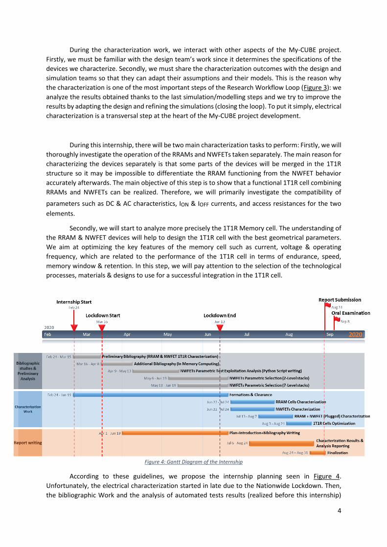
Figure 6: 42 Years of microprocessor trend data (from [17])
Since 2006, this trend has come to a halt. The number of transistors per chip is still increasing
but the Dennard Scaling Rule is not true anymore and the power efficiency & performance are
plateauing. Indeed, let us consider the power P used by a CMOS chip [18]:
𝑃 = αQfCV2 + 𝑉𝐼𝑙𝑒𝑎𝑘𝑎𝑔𝑒 ,
Equation 1: CMOS Power Consumption
with α the activity factor (proportion of the circuit in activity), Q the number of transistors, f
the operating frequency, C the capacitance, V the operating voltage and Ileakage the leakage current.
The static-power term in Equation 1 could be neglected if the feature size stayed above the 65-nm
node. During this period, Dennard scaling rules allowed to keep the total power used constant since
most of the transistor count rise and operating frequency increase were balanced by capacitance and
operating voltage downscaling.
However, static power became the dominant term in the CMOS chip power equation since leakage
current is exponentially rising with feature size shrinking. Moreover, the operating frequency of CMOS
circuits cannot be sustained by using lower operating voltages (capacitances are slower to load at
lower voltages). The operating voltage downscaling came to a halt around a value of 0.8V for the last
generations of CMOS technologies.
In this so-called post-Dennard-scaling era, various improvements had to be introduced at the
dynamic-power-consumption level to keep scaling transistors with a limited energy-efficiency because
of constant operating voltage. One way to keep increasing the transistor count has been to switch-off
unused parts of the chip at runtime, the so-called “dark silicon”. However, this type of improvement is
only susceptible to increase the energy-efficiency of 40% per generation, which is insufficient to keep
improving the performances at the Dennard scaling pace [18].
In parallel, the issue of leakage power had to be addressed to reduce the exponential static power
consumption. It was done by using new types of CMOS architecture such as FinFETs that benefit of a
much better channel electrostatic control. For instance, Double-Gate (DG) and Tri-Gate (TG) FinFETs

8
exhibit smaller DIBL values than state-of-the-art MOSFETs (ETSOI) in Figure 7-b. Indeed, FinFETs benefit
from the so-called enrobing gate configuration where the contact between the fin-shaped channel and
the gate is in three directions (Figure 7-a - right). FinFETs do not only exhibit less short-channel effects
than MOSFETs but also faster switching times and higher current density. For these reasons, FinFETs
became the dominant gate design (starting from the 22nm node) for modern nanoelectronic device
fabrication [19].
Figure 7: a) Structure of bulk MOSFET and FinFET and b) DIBL values for different FET technologies [20] [21]
However, even FinFETs reach their limits when dimensions are shrank even further. The main
problem with FinFETs is that their height is growing and their thickness is shrinking with each node. In
particular, any increase of driving current comes at the expense of a fin height increase. This increase
of height cannot be sustained indefinitely from a technological point of view. Indeed, when
approaching the 15 nm gate length, it is becoming difficult to fit FinFETs in standard cells while keeping
a good electrostatics control [22]. In the coming technological nodes, it will be necessary to dispose of
easily scalable devices with even better immunity to short-channel-effects.
In the following, we will see that the so-called Gate-All-Around Nanowire Field Effect Transistor
(GAA NWFET) is the best-suited candidate to replace the FinFET in terms of electrostatic control.
Moreover, it can be enlarged for a better drivability (Nanosheet).
III)1)a)ii) NWFET Structure & operation
The Gate-All-Around Silicon Nanowire is the next technological step after the FinFET. The main
idea of the GAA architecture is to dispose of a channel with an enrobing gate on all four sides. This is a
FinFET with gate enrobing under the channel. Figure 8 shows the geometry of such device compared
to a FinFET. This is called a nanowire because the channel looks like a suspended “wire” encapsulated
in the gate. GAA transistors are often considered as the ultimate technology in terms of immunity to
short-channel-effects (Figure 8 - Middle). In addition, NWFETs are fabricated with limited deviation
from FinFET manufacturing process [23]. The second huge advantage of this technology is that
nanowires can be stacked on top of each other (Figure 8 - Middle) to improve the drive current per
footprint. The use of the third dimension can be a huge enabler to increase the chip device density
a) b)

9
especially if the number of levels is high. Recently, stacks of up to seven nanowire layers have been
demonstrated [24].
Figure 8: Structure of FinFET, GAA-NWFETs and GAA-Nanosheets [20]
Nevertheless, the driving current provided by a single wire is limited because of the nanowire
cross-section size. The best solution so far has been to tune the nanowire cross-section width to form
the so-called Nanosheets (Figure 8 - Right). These devices can drive a much higher current (per
footprint) depending on their size but they still benefit from great electrostatics [25]. Therefore,
stacked-Nanosheets exhibit very low DIBL values (<100mv/V) and much reduced leakage current
overall (1nA/µm) [26].
Two issues remain for the use of Stacked-Nanosheet in the My-CUBE project array. Firstly, the
driving current of the NWFETs may be too low, even after adopting the Nanosheet geometry. Indeed,
this technology has been primarily developed for CMOS use where the stacking of several nanowire
levels allows to drive high currents. In the My-CUBE project however, each nanowire will have to drive
one RRAM cell. It negates the stacking high current benefits. Nanosheet width extension cannot
continue indefinitely without degrading electrostatics or disturbing the fabrication process at some
point. The other hurdle is the NWFETs access resistance, which is much higher than usual MOSFET’s.
This high parasitic resistance may prevent us from setting correctly the RRAMs (because less current
is available). It could also be difficult to read the written cells afterwards if the access resistance is not
negligible compared to the RRAM resistive states values.
We discussed the state-of-the-art Gate-All-Around Nanowire FET technology for integration in
the My-CUBE array. The transistor plays the role of a selector in the 1T1R cell: it only controls the
amount of current flowing through the memory point. In the following, we will investigate the main
part of the 1T1R cells we are designing: The Resistive Random Access Memory (RRAM).
III)1)b) RRAM operation, materials and electrical properties
III)1)b)i) RRAM Context
Memory is one of the essential parts of any computing architecture. It can be either of the
classical Von Neumann type or emerging like My-CUBE. In the past, the role of memory was to store
program-related data with solid state DRAM and compact magnetic hard disk drives. With the
invention of the NAND flash memory, it became possible to store a huge volume of general information
because these non-volatile memories are very cheap. In the recent years, the performances of usual
memories have slowly increased while the demand of memory for information storage has been

10
booming. Indeed, customers have been requiring an ever-increasing resolution and quality, which
leads to a constant need for technology growth [27].
According to the trends mentioned above, the current state of the semiconductor memory
market is the following (Figure 9-a): it is split between the two main memory families which are volatile
memories with DRAM (53%) and non-volatile with Flash Memories (NAND/NOR, 45%). DRAM is based
on conventional CMOS technology : one cell contains one MOSFET paired with a simple capacitor
which is storing the information as long as it is not discharged. That is why this type of memory is
volatile : the capacitor is slowly discharging because of the leakage current of the MOSFET and they
need to be refreshed at least once each 64ms for each cell according to the Joint Electron Device
Engineering Council (JEDEC) standards [28]. On the other hand, Flash Memories rely on floating-gate
MOSFETs. These transistors possess a double-gate structure with a control-gate and a floating-gate.
The floating gate is electrically insulated so its charge can remain unchanged for long periods of time.
This is where information can be stored. This memory is considered non-volatile since no refresh is
really necessary once the information has been written.
Together, these two technologies represent approximately 97% of the memory market
volume. There are dozens of other emerging memory types such as Magnetic RAM (MRAM) which
stores information in electronic spin [29] and Phase-Change RAM (PRAM) which relies on rapid heat-
controlled changes between amorphous and crystalline states which have different resistance values
[30]. These non-volatile emerging memory-types are usually less energy-expensive and faster than
DRAM and Flash memories overall [31]. But they account for a small fraction (3%) of the memory
market because of their very high commercialization costs compared to Flash and DRAM memories.
So far, it has been more cost-effective to improve existing memory technologies than to introduce
emerging memory technologies. But similarly as the Moore’s Law governing transistor sizes, it is
becoming increasingly difficult and expensive to build-up performance with existing technologies. In
the Figure 9-b, NAND Flash storage capacity is rising at a slower rate than other memory technologies
such as PRAM, MRAM and RRAM. For this reason, RRAM was considered as a future challenger for
NAND Flash. But since 2015, NAND Flash has been scaled further down and a no NAND replacement is
in sight for the years to come. On the long run though, memristors such as RRAM and PRAM still have
a higher scaling potential compared to charge-storage devices such as Flash or DRAM [32] [33].
Figure 9: a) Semiconductor Memory Market (2020 forecast) (IC Insights) and b) Storage capacity (MB) of different memory types since 2001 (ISSCC 2019)
a) b)

11
However, there are other fields where RRAM shows great potential apart from mass-storage
memory. Indeed, Resistive Random Access Memory is one of the most mature candidates for future
use in the electronics industry and exhibits some of the fastest writing & reading times, low energy
and leakage as well as being non-volatile and quite scalable [31] [34] [35]. For these reasons, this
memory technology is currently under consideration for In-Memory Computing applications and for
use in Neural Networking chips [32] [36] [37].
One possible explanation to the remarkable properties of this memory is its atomic filament-
based storage mechanism. The next part will detail this theory along with the operation of several
RRAM types.
III)1)b)ii) RRAM operation
Resistive Random Access Memory is a type of memory which can be used for computing. It
works by changing the resistance across a dielectric solid-state material [38]. They are based on a
Metal-Insulator-Metal (MIM) structure which can be seen in Figure 10 a. RRAM relies on structural
modifications across the insulating layer whereas classical memories such as Flash and DRAM work
thanks to charge storage mechanisms (in a double-gate or in a capacitor). RRAMs can reversibly switch
between two distinct resistive states: it can be SET to a Low Resistive State (LRS) and RESET to a High
Resistive State (HRS), which respectively correspond to the logical states “1” and “0”. The widespread
explanation of this behavior is the so-called Conductive Filament (CF) model: a conductive path is
formed or dissolved across the dielectric layer if appropriate electrical field conditions are applied on
the MIM stack. A distinction exists depending on the type of electrical field to apply: the cell is Bipolar
if the polarity of the electrical field changes between SET and RESET operations (Figure 10 b). The cell
is Unipolar if the polarity does not matter for SET and RESET operations (Figure 10 c).
Figure 10: MIM structure and different ideal RRAM characteristic diagrams (from [11])
Many different types of MIM stacks can exhibit resistive-switching properties and several of
them have been used for making RRAM cells [11] [34]. At this point, we shall differentiate two types
of RRAM devices according to the nature of the conductive filament used: Conductive Bridge RRAM
(CBRAM) that relies on a metallic-ion filament formed in a solid electrolyte and Oxygen vacancies
filament-based RRAM (OxRAM) [34]. OxRAM is the most common type reported in the literature and
Voltage
Bottom Electrode
Dielectric Layer
Top Electrode
a) MIM Structure b) Bipolar RRAM c) Unipolar RRAM

12
we will focus on it in the following of this report. An oxygen vacancies conductive filament model
allows explaining the operation of the RRAM cells as we can see in Figure 11 for the bipolar type.
First, the pristine OxRAM cell must experience a soft dielectric breakdown prior to reversible
resistive switching. This preliminary step is called Forming and does happen only once when using
pristine cells (Figure 11.1). During the forming, a strong positive voltage VForming is applied on the top
electrode. Oxygen atoms are knocked out of the insulator lattice, creating oxygen vacancies inside of
it ( ) while oxygen ions ( ) migrate towards the cathode interface. The RRAM cell is now in LRS
since a conductive filament of oxygen vacancies exists between the top and bottom electrode (Figure
11.2). The cell will retain its LRS state while the voltage applied on the top electrode stays positive or
null.
A LRS OxRAM cell can be switched to HRS state if a voltage of enough amplitude VReset is applied
on the bottom electrode. This operation is called RESET and it is the opposite of the previous operation:
oxygen ions migrate from the top electrode interface to fill some of the closest oxygen vacancies left
in the dielectric layer (Figure 11.3). The RRAM cell is now in HRS since the conductive filament does
not exist anymore between the top and bottom electrode, even though some part of it still subsists in
the dielectric layer (Figure 11.4). The cell will retain its HRS state while the voltage applied on the top
electrode stays negative or null.
It is possible to return to the LRS state by re-applying a positive voltage VSET on the top
electrode. Similarly to the forming operation, the conductive filament reappears while oxygen ions
migrate towards the cathode interface. This operation is called SET (Figure 11.5). The difference with
the forming is that the voltage needed for a soft dielectric breakdown is lower since part of the filament
still subsists in the insulating layer (0 < VSET < VForming).
Figure 11: RRAM Conductive Filament Forming and Cycling Principle
1. Forming 2. LRS 3. RESET
4. HRS 5. SET 0. Pristine RRAM cell
Top Electrode
Dielectric Layer
Bottom Electrode
VForming > 0 VReset > 0
VSet > 0

13
The cycling of a RRAM cell consists in a sequence of successive SET & RESET operations (Figure
11.2, 3, 4, 5). Electrically, we can see the cycling operations on the I-V characteristic of the Bipolar
RRAM cells (Figure 12). We can notice on Figure 12 the LRS (blue) and the HRS (red) which correspond
to a linear ohmic behavior of the cell. In-between these two stable states are the SET (HRS to LRS) and
RESET (LRS to HRS) transitions where the resistance of the cell changes. During the SET operation, the
cell is experiencing a sudden drop of resistance and a spike of current. It is necessary to limit the current
spike happening in the memory cell to prevent potential damage. Therefore, RRAM cells are usually
coupled with transistors inside of a 1T1R structure where the transistor play the role of a current limiter
and/or interrupter.
Two main parameters will determine the switching behavior of the RRAM cell: the compliance
current during the SET operation (Ic) and the maximum absolute voltage applied during the RESET
operation (Vresetstop). In the following part, we will discuss the impact of such parameters on the RRAM
cell operation.
III)1)b)iii) RRAM parameters influence
As we previously saw, RRAM cells are memory devices that can reversibly switch between two
distinct resistive states: LRS and HRS. The memory cell is retaining its HRS / LRS state if the operating
point is weak (low operating voltage). As we explained in part III)1)b)ii), if the operating voltage is
increased in the negative or positive range, SET or RESET transitions can take place and the resistive
state of the cell changes. The resistance value achieved for each resistive state will heavily depend on
the electric field applied during the SET and RESET transitions.
During the SET, the RRAM cell is switching from HRS to LRS and a spike of current takes place.
This transition can be described with Vset which is the voltage associated with the current spike and
the compliance current Ic, the upper limit of the current allowed to flow through the RRAM cell (Figure
12). The value of the compliance current IC is the SET controlling parameter since VSET cannot be used
to control the current spike magnitude in a practical way.
On the opposite, a cell in a RESET transition is difficult to control with current. Indeed, the cell
is going from LRS to HRS thus experiencing an increase in resistance and a decrease in current if the
voltage increases. This transition is less brutal than the SET (Figure 12). The key parameter for the
RESET will be the Vresetstop voltage i.e. the maximal (negative) voltage reached during the operation.
Indeed, Vresetstop is related to the maximal resistance attained by the cell. It stays stable when the
applied voltage goes back to 0V, thus corresponding to the HRS state value.

14
Figure 12: Bipolar RRAM detailed I-V Characteristic
Together, Vresetstop and Ic allow to control the resistance values of HRS & LRS states and the
memory window (MW) of the cell. The Memory Window is the margin or difference that exists
between the LRS and the HRS states (in resistance or in current). If the memory window is close to 0,
it prevents the use of the memory cell since we cannot clearly differentiate the different information
that will be coded in the cells. As shown in Figure 13, Vresetstop has a strong effect on the RRAM HRS
values for the same cell: the higher the Vresetstop, the higher the HRS values, the higher the MW since
LRS values stay constant (the MW is the difference between curves of the same color in Figure 13).
Concerning Ic, we can see that increasing this parameter decreases both LRS and HRS values.
Therefore, it has only a limited impact on the MW of single cells (no increase of the difference between
two colors when moving to the right of Figure 13).
Figure 13: LRS & HRS dependence on programming parameters Ic & Vresetstop for a single memory cell (from [39])
SET
RESET

15
Nevertheless, it is not enough to consider single cells MW when looking at arrays containing
multiple RRAM cells operating during thousands of cycles. In this case, the MW is the difference
between the worst LRS and the worst HRS. Indeed, we must always be able to differentiate LRS & HRS
for any cell for preventing errors. In short, the cell-to-cell/cycle-to-cycle variability must be considered
when looking at the operation of a RRAM array. This is of utmost importance because it means that
the 1% worst cells of the LRS/HRS distributions will have a disproportionate influence on RRAM arrays
performance, no matter the behavior of the 99% other good-working cells.
It has been shown that increasing the value of Ic can drastically improve the MW of RRAM
arrays because it reduces the cell-to-cell/cycle-to-cycle variability of the LRS state [40]. Indeed, we can
see on Figure 14 that the distributions representing the LRS states of 7 different cells during 1000 cycles
are much stiffer with IC. It leads to a considerable improvement of the global MW in this case. More
generally, the impact of IC on the MW will also depend on the value of VResetstop. Nevertheless, the cycle-
to-cycle variability is fundamentally different from the cell-to-cell variability and one type of variability
may even be predominant depending on the properties of the cells under study [41].
Figure 14: LRS & HRS dependence on Ic (7 cells & 1000 cycles) (from [39] )
Apart from the MW, another important metric concerning RRAM cells is their endurance. The
endurance is the maximum number of write cycles (Set+Reset) that a cell can sustain while keeping a
positive MW. Concerning the endurance of the RRAM cells, the main influencing factor seems to be
Vresetstop. Indeed, it has been reported that increasing Vresetstop leads to a reduced endurance [42]. More
generally, there is always a tradeoff between the MW and the endurance of RRAM cells.
To conclude, Vresetstop and Ic are the two main parameters enabling to control the behavior of
RRAM cells. Together, these parameters will influence the memory window, the endurance and the
variability of the cells. Therefore, it is important to control the polarization of RRAM cells in an accurate
way to achieve desired properties. Because of this, RRAM cells are usually paired with transistors inside
of so-called 1T1R structures. We will detail the properties and the architecture chosen for the My-
CUBE project.

16
III)1)c) 1T1R Memory cells structure, architecture and My-CUBE memory pillar
There are several memory architectures based on RRAM cells. The two main approaches are
the cross-point array (Figure 15) and the 1T1R array (Figure 16). In the cross-point array, simpler
selector such as diodes can be used instead of transistors (their role is to prevent leakage in unselected
cells). The voltages applied on the Bit Line (BL) and the Word Line (WL) select the cells [43] [44]. The
main advantage of this type of structure is that since no “real” selector is needed, the memory stacks
can be “sandwiched” in-between the WL and the BL with a high density (Figure 15-c). Moreover, it
allows resorting to Back-End Of the Line (BEOL) process for the fabrication of the RRAM cells.
Consequently, the implementation of peripheral circuits is done underneath the cross-point array and
it greatly reduces the circuitry overhead [45]. The drawbacks of such structure include limited energy-
efficiency due to leakage currents in unselected cells and complex read and write operations making
the selection of individual cells more difficult.
Figure 15: a) Cross-point cell b) Cross-point array structure c) 3D perspective
More conventionally, each RRAM cell can be paired with a transistor inside of a 1T1R structure
(Figure 16 - a). This topic was detailed in the previous part [III)1)b)ii)]. In particular, the presence of
such a selector allows enforcing the compliance current during the Forming and Set operations to
prevent RRAM cell damage. Literature shows that using a 1T1R structure is also better in terms of
endurance, variability and MW [40]. Concerning our In-Memory-Computing application within the My-
CUBE project, the 1T1R structure has been preferred since it allows controlling directly which cells are
active, as seen in Figure 16 - b .
RRAM
Selector
a)
b) c)
17
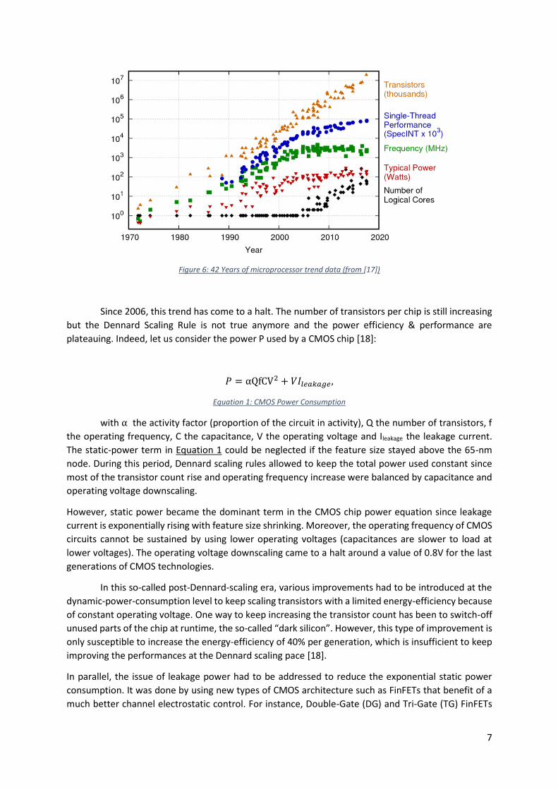
Figure 16: a) 1T1R Cell and b) Detailed connections of the My-CUBE RRAM structure
Indeed, My-CUBE project team aims at fabricating a 3D RRAM architecture in which basic
logical operations can be performed. In particular, the architecture adopted is a so-called 3D memory
pillar made from 1T1R cells (Figure 16 - b). This structure allows summing the currents flowing through
each cell constituting the pillar. Therefore, this structure allows realizing a summing operation of the
information contained by any combination of cells belonging to the pillar if we can select the right cells
electrically. The use of the 1T1R structure allows selecting single memory cells in this 3D structure for
performing this type of In-Memory computations. The main drawback of using 1T1R cells for the My-
CUBE chip is a higher footprint per memory cell. This disadvantage may be compensated by the 3D
structure, which allows stacking RRAM levels on top of another. It increases the density of the circuit
by a factor equal to the number of stacked layers (four different layers are shown in Figure 16 - b).
The following section will explain how to exploit the My-CUBE RRAM structure to perform In-
Memory-Computations. We will use a promising memristor-based approach called Scouting Logic.
III)1)d) Memristors-based logic functions : Scouting Logic
The operation of the final My-CUBE chip will rely on the so-called Scouting Logic for performing
simple logic operations within its memory pillar structure. This innovative approach is based on reading
operations. It allows to do fewer gate executions than other solutions proposed in the literature [46]
(which is costly in terms of endurance with RRAMs). According to literature, scouting-logic is faster,
more efficient and has less footprint than other state-of-the-art RRAM logic design styles [46].
The main idea behind this concept is to observe sums of currents representing RRAM states
and to perform operations by changing the reading current. We will explain it with the simplest
a)
b)
NWFET RRAM
1T1R Cell

18
scouting logic configuration with 2 RRAM cells in parallel (Figure 17-a). The information encoded in the
two RRAM cells represent two variable values (X & Y). Since both cells are in parallel, we will have
IOUT=Iread(X) +Iread(Y). The different cases with the combinations of LRS/HRS currents are shown in Figure
17-b. The idea is now to use a sense amplifier (SA) to compare IOUT with a reference current Iref that is
chosen depending on the operation we want to perform. As shown in Figure 17-a, if Iout > Iref then Vout
= 1 and if Iout<Iref then Vout = 0.
For example, if we set Iref in the window between LRS // HRS and LRS // LRS (Figure 17-b) we
will perform an AND operation when reading. Indeed, if X or Y is 0, IOUT will end up left of Iref in Figure
17-b and the result is compare(IOUT,Iref)=0. But if X=Y=1 then IOUT will be greater than Iref and
compare(IOUT,Iref)=1. This is exactly the truth table of the AND operation (Figure 17-c).
Figure 17: a) SL electrical configuration, b) SL basic operations and c) associated truth table (from M. Ezzadeen)
One issue with scouting logic though, is that you need to have very distinct RRAM states.
Indeed, we cannot perform any type of operation if there is no memory window in between the three
blue distribution in Figure 17-b. Therefore, it will be very important to have acceptable RRAM
performance if we want to perform computations.
Iout
(µA) 2 HRS 1 LRS
1 HRS
0 0
2 LRS
0 1
1 0 1 1
OR AND
a) b)
X
Y
c)

19
In the next part, we will detail the objectives of this internship: we will explain how we plan to
characterize these novel 1T1R cells for a successful integration in the My-CUBE structure. We will also
investigate how to assess their use for scouting logic.
III)2) Internship objectives
As we mentioned in the introductory part of this report, there will be two main
characterization tasks to perform during this internship:
- Firstly, we will thoroughly investigate the operation of RRAMs and NWFETs taken
separately. Our goal is to demonstrate that they may be used together for making
functional 1T1R memory cells.
- Secondly, we will start to analyze more precisely the operation of 1T1R Memory cell. The
understanding of the RRAM & NWFET devices will help to design the 1T1R cell with the
best tradeoffs and the best performances for In-Memory-Computing.
In the following, we will first present how we plan to characterize the functionality of NWFETs
and RRAMs and we will detail the experimental setup used. The second part will present about the
performance of RRAMs and NWFETs. It will focus on the expected tradeoffs we will have to consider
during this work.
III)2)a) Electrical Characterization and device performance
The main reason for characterizing the devices separately is that some parts of the devices will
be merged in the 1T1R structure so it may be impossible to differentiate the RRAM operation from the
NWFET behavior accurately afterwards. The second reason, which is more practical, is that the
integration of RRAMs together with NWFETs has only started in the framework of the My-CUBE project
and no wafer involving this structure is available for testing yet.
The main objective of this step is to show that a 1T1R RRAM array combining RRAMs and
NWFETs can be fabricated and used for In-Memory-Computing purposes. Therefore, we will primarily
investigate the compatibility of parameters such as DC & AC characteristics, ION & IOFF currents, the
operation bias and access resistances for the two elements. In the following, we will explain how to
perform this characterization work on NWFETs and on 1T1R RRAM array (with bulk MOSFETs as
selectors).
III)2)a)i) NWFET (1T) Characterization
The electrical characterization of NWFETs transistors will be realized thanks to two different
setups:
- Firstly, we will analyze many different devices with a so-called parametric automatic
testing setup. This kind of test provides a rough idea about the functionality and
performance of the devices. Typically, this test is done on many dies to extract meaningful

20
performance metrics such as: Drain Induced Barrier Lowering (DIBL), Threshold voltage
(Vth), Saturation current (Isat ), Subthreshold Slope (SS), etc. This step allows to study a great
number of devices and select the transistors with the best performances for further study:
for example, Figure 18 shows some of the results of this type of test concerning 3 different
types of NWFET geometries measured over 10 different dies each. This task is done in
cooperation with CEA-LETI nanocharacterization lab since the use of a PrecioNano© paired
with an Agilent 4080 Series© is needed to conduct such extensive testing.
- Secondly, we will focus on the devices that have been selected in the first step and we will
perform advanced electrical characterization on them. The goal of this step is to extract
specific devices meaningful data such as Id-Vg & Id-Vd characteristics (Figure 19). By
extracting these data, we will have a precise understanding of the operation of these
devices on a wide range of operating conditions. This type of setup is more flexible and
allows custom-testing such as high-polarization tests. The electrical setup for this test
involves a Keysight Technologies B1500A Semiconductor Device Analyzer© paired with a
probe station.
Concerning NWFET characterization principle, it is the same for the two sets of experiments:
four probing tips are connected to the different pins of each transistor (Bulk/Source/Drain/Gate) and
specific polarizations are directly applied on the device.
Device 1 Device 2 Device 3
Wafer 5 5 5
L=Length (nm)
W=Width (nm)
30 50 50 50 50 80
IsatN (µA.µm-1) 353.6 (±43.2) 354.7 (±20.5) 340.4 (±24.7)
DIBL 0.0604 (±0.0588) 0.0236 (±0.0041) 0.0255 (±0.0050)
Ron (Ohm.µm) 734.81 (±38.08) 784.78 (±45.06) 812.45 (±42.35)
SS (VD=0,05V) (mV/dec)
75.656 (±9.253) 67.483 (±1.982) 69.439 (±1.990)
Vtsat (VD=0,9V) (V) 0.5321 (±0.0991) 0.6225 (±0.0190) 0.6227 (±0.0176)
Figure 18: Typical parametric test results (3 devices over 10 dies) performed on GAA stacked-Nanowires FETs
a) b)
Figure 19: Typical NWFET polarization test characteristics: a) Id-Vd b) Id-Vg plots performed on GAA stacked-Nanowires FETs
Id (
µA
)
Id (
µA
)
Vg (V) Vd (V)

21
III)2)a)ii) RRAM (1T1R) Characterization
Concerning the RRAM memory stack, we will use two different experimental setups:
- Firstly, we will study single memory cells and extract the best operating conditions in terms
of memory window and failure probability (Figure 20). We will consider this set of
conditions with respect to the NWFET data. We will check the compatibility of the new
selector with the RRAM memory. Such measurement is usually done on a great number of
cells (100+) (Figure 20-b), thus considering RRAM cell-to-cell variability. The
characterization of RRAM memory cells is therefore more complicated than NWFETs and
it will involve a 4090µ+ Electroglas© paired with a Keysight technologies B1500A© along
with an Arduino Microcontroller©.
- Secondly, some In-Memory-Computing functionalities from the My-CUBE chip will be
demonstrated using a RRAM array. We will prove that simple computing operations can
be done with the help of such array. Moreover, this experiment will be conducted using
NWFET-compatible operating conditions (extracted from III)2)a)i) ). For such a task, the
use of a PrecioNano© paired with an Agilent 4080 Series© will be needed since the
programming of multiple RRAM cells in the same array is required.
In fact, every experiment involving RRAM cells in this part will be done with 1T1R cells where
CMOS transistors are used as selectors. Indeed, as we saw in part III)1)c), the 1T1R structure allows a
good control of the current flowing in the memory cell, and greatly enhances the cells performance.
However, the 1T1R structure is electrically different from a 1R structure such as the one we
focused on in part III)1)b). Indeed, we can only measure the total 1T1R cell voltage (V1T1R) and not
directly the memory cell (VR) and the selector voltage (Vselector ). Indeed, we only have access to three
different pins on such 1T1R structure (probing point in Figure 21). It has been shown, that it is possible
to recover VR and Vselector from V1T1R if the I-V characteristics of the transistor and memory cell are
known [39]. The transistor is mostly used during the SET operation with its gate voltage (Vg) associated
to IC. IC is one of the key parameters according to III)1)b)iii). During RESET & READ operations, the
transistor is wide-open (high Vg is applied) so that its parasitic influence on the 1R cell (voltage-drop)
is minimal.
In the following, we will neglect effects arising from the transistor during the reading for two
reasons: Firstly, we are mostly interested in comparing currents flowing through cells with the same
type of selectors in the scope of this study. Indeed, we will compare 1T1R cells between each other,
thus reducing the impact of the transistor voltage drop during the read operation. Secondly, the final
target of this study is the co-integration of RRAMs with NWFETs inside of a 1T1R structure. Therefore,
a parasitic behavior will still be present in the final structure because of the NWFET selector.

22
Figure 20: Typical RRAM results a) CDF 100 cells 1 cycle b) Cycling 100 cells 10k cycles
Figure 21: 1T1R Characterization Setup
III)2)b) Optimization of 1T1R cells and expected tradeoffs
It has been shown that NWFETs or Nanosheets can usually drive currents up to several tens of
µA in the best cases [24] [47]. Even by adopting a wider Nanosheet configuration, it is likely to be
difficult to drive RRAM memory cells with such low currents. Indeed, most RRAM cells usually rely on
hundreds of µA as compliance currents [39] [41] [48]. As can be seen in Figure 14, we cannot reach
any sufficient MW under 150µA for the devices of this example. This mismatch between the usual
NWFET performance and the regular polarization of RRAM cells in terms of driving current is a great
difficulty for the co-integration of these two advanced technologies into functional 1T1R memory cells.
Vselector
VR
: probing tip location
a) b)
SET RESET
MW
MW SET
RESET

23
Indeed, it has been seen in part III)1)b)iii) that the compliance current was one the two main
parameters determining RRAM performance.
In this part, we will see which strategies we put in place to bridge this driving current gap. We
will focus on increasing the driving current of regular NWFETs, lower the compliance current of RRAM
cells while maintaining MW and failure rate performance. Eventually we will also consider design
strategies such as double coding to reduce this problem. The different approaches are summarized in
Figure 22.
Figure 22: Driving current optimization strategies used
III)2)b)i) NWFETS (drive current / polarization / drift)
Concerning NWFETs, two strategies can be implemented to increase the saturation current of
the devices: at the geometry level, it is possible to rely on NWFETs with large widths (so-called
Nanosheets) which can drive more current. However, expanding the width of such Nanosheets too
aggressively may lead to process issues for the transistor. Indeed, stacked Nanosheets may collapse
on top of each other during the fabrication process because the sheets are suspended on top of each
other at some point. The current state-of-the-art in terms of dimensions for GAA Stacked-Nanosheets
is a maximum width of 85nm across 7-levels stacked wires [24].
The second option to increase the current driven by a given NWFET transistor is to increase
the supply voltage. Indeed, increasing the Gate Voltage Vg and the Drain Voltage VD beyond the usual
polarization range (for CMOS applications) will probably allow increasing ID. This approach is quite risky
since we do not know if such aggressive conditions may damage the device over time by drifting its
electrical characteristics for example. However, since we are using this type of transistor as an RRAM
selector, the usual endurance constraints are more relaxed compared to a full-processor application.
Writing and Erasing the RRAM memory should not remain a very frequent operation thus soliciting the
NWFET selector less often.
We will apply these two strategies during this internship. Nevertheless, we do not expect the
resulting increase of NWFET drive current to be enough for using RRAM cells in optimal operating

24
conditions. In the next part, we will try to lower this operating current while maintaining acceptable
performance on the RRAM side.
III)2)b)ii) RRAMS (drive current / MW / endurance )
It was shown in part III)1)b) that RRAM performance was highly dependent of the couple of
parameters VResetstop & Ic . The impact of these two parameters on the RRAM cells operation is multiple
and affects the MW, the failure rate, the endurance etc.
We will optimize the different parameters playing a role in the functioning of RRAM cells
(including but not limited to IC). The objective of this set of experiments is to find a compromise
between compliance current (IC), the good operation of the memory cells and the other RRAM
parameters. For instance, we may have to consider smaller MW for operating at low IC as seen in
III)1)c).
Even after these NWFET & RRAM optimizations, it is still possible that driving currents do not
match. The last option we can resort to is to introduce redundancy at the design level to improve the
performance of RRAM cells with a lower operating current.
III)2)b)iii) Design level (drive current / double coding = footprint )
The primary operation of the My-CUBE chip will rely on the capacity to read the currents and
to differentiate currents flowing through RRAM cells in LRS state (logic “1”) from currents flowing
through RRAM cells in HRS state (logic “0”). As we discussed in part III)1)b)iii), these are the extreme
values of LRS and HRS states that will have the greater impact on the final performance of the RRAM
cell in terms of MW and failure probability. However, these values are mere errors that only a very low
probability to happen.
One idea to enhance RRAM performance is to make the cell information redundant. One
example of this is the so-called double coding technique: we start by coding each bit of information in
two contiguous cells instead of one. The current representing the same state of the two cells is read in
parallel. It can be seen in Figure 23: in this case, we have iread = i1 + i2. Therefore, any extreme value of
current i1 has a chance to be compensated by a regular value of i2 when looking at the values of iread.
In other terms, the probability of reading an “extreme” value with iread is the probability that both i1
and i2 are extreme, thus reducing the impact of extreme values in iread. This type of strategy has the
potential to improve RRAM cells performance.
Figure 23: Double-coding principle
Cell 2
Cell 1
Same information

25
The problem with this approach is that it doubles the footprint of the circuit compared to
simple coding at equal computing performance. We consider that the 3D stacking of memory cell levels
as described in the My-CUBE architecture will compensate for this inconvenient.
This design idea will be exploited to compensate for the lower operating current of the cells
when performing logic operations. We will see in the following that the operation of the My-CUBE chip
relies on so-called Scouting-Logic, which is a novel way for doing In-Memory-Computing calculations.
Other scientific perspectives at the fabrication-level will also be discussed.
IV) Process flow / fabrication
This part is dedicated to the main fabrication challenges of the different structures analyzed
throughout this work: stacked-Nanowire FETs, BEOL OxRAM, My-CUBE chip, etc. We will also present
in this part the process flows associated with each device.
IV)1) Stacked-Nanowire FETs
As mentioned in part III)1)a)ii), one attractive advantage of NWFETs is that they can be
manufactured with limited deviation from regular FinFET fabrication process [23]. In the following, we
will focus on the steps that are specific to the Stacked-Nanowire structure. These steps are presented
in Figure 24 with the yellow parts being specific to stacked-NWFETs fabrication. Manufacturing
stacked-NWFETs relies on a so-called Replacement Metal-Gate (RMG) approach: the metallic gate is
deposited at the very end of the process flow. This technique allows having a better gate oxide and
better strain from S/D SiGe [49].
The first step for manufacturing stacked-wires FETs is the epitaxial growth of multilayers
corresponding to the number of stacked-wires desired. An example with seven stacked-channels is
show in Figure 25–a. Following this deposition, fins arrays are patterned to fabricate stacked-wires
FETs. Dummy gates and spacers are then added before etching sacrificial SiGe layers. These SiGe layers
are selectively etched to introduce well-aligned and correctly sized so-called Inner Spacers. The
presence of these so-called Inner Spacers in-between the Si channels (Figure 25-b/c) is essential
because they help reduce parasitic capacitances. The source and drain are then grown by epitaxy and
the dummy gate is removed.
Then, the release of the Si is performed during the RMG module prior to conformal
HfO2/TiN/W gate deposition (Figure 25-d). Finally, self-aligned-contacts are defined for the source and
the drain. It means that contacts are selectively etched, leading to relaxed lithography constraints
during this step [50]. The result of this step is seen in Figure 25-e.
The main takeaway from this complex process flow is that the number of stacked wires does
not add much to the overall fabrication complexity since stacks of 13 levels have already been
manufactured with this technique [51]. On the other hand, the tuning of the 2D-dimensions of the
NWFETs seems a bit less easy in terms of fabrication process but widths ranging from 15nm to 85nm
have also been demonstrated: Figure 25-f shows the final morphology of such 7-stacked-levels
nanowires.

26
Figure 24: Process flow for fabricating vertically stacked-wires MOSFETs in a replacement metal gate process (from [23])
Nan
Figure 25: Main fabrication steps of vertically stacked-wires MOSFETs in a replacement metal gate process (from [23] [24])
In the following, we will detail the general fabrication process of RRAM HfO2 MIM stacks. We
will take as an example the ones that we will characterize during this internship.
IV)2) BEOL fabricated OxRAM
In general, RRAM are realized in BEOL process. This is the case for the devices we will
characterize in this internship. The general structure is shown in Figure 26: the RRAM stack (Figure
a) b) c)
d) e)
a) (Si/SiGe)
EPI growth
b) (Si/SiGe) Fin patterning
b) Inner spacer formation and c) TEM image d) SEM image after dummy-gate etching
and after release of Si channels
e) TEM image and EDS spectroscopy after
the fabrication of self-aligned-contacts.
f) TEM images and EDS spectroscopy of GAA NS transistors
with 7 stacked channels (15nm≤W≤85nm).
f)

27
26-a) is deposited in-between top metal layers M1 and M2 on top of the MOSFET drain contact
(Figure 26-b).
Figure 26: 1T1R BEOL structure with MIM stack detail
For the 1T1R cells we characterized, the CMOS part is fabricated with conventional CMOS
130nm technology and is outsourced from an industrial partner (STMicroelectronics). This industrial
partner also does the first four Cu metal layers (Figure 26-b). The different layers constituting the
RRAM memory stack as well as the fourth and fifth metal layers are deposited using physical vapor
deposition (PVD) at 300 – 440°C at CEA-LETI cleanrooms.
The first memory stack layer is made from TiN. It plays the role of the bottom electrode and it
is deposited on top of Metal 4 (Figure 26-a). One function of this layer is to grip the Metal4 layer with
the memory cell [11]. It is followed by the deposition of the active layer of the memory cell, which is a
5nm thick HfO2 oxide. This is in this layer that the conductive filament formation/annealing mentioned
in section III)1)b)ii) takes place. On top of that is deposited a top electrode made from a Ti/TiN bilayer.
After deposition of Metal 5 above the RRAM stack, an etching step is usually carried on Metal 5 and
the active materials to better define the memory cell [11].
Once fabrication is completed, three (plus one) different contacts are available for the
characterization of the 1T1R cells: The transistor source and gate as well as the top electrode of the
RRAM stack (plus the bulk). As mentioned in section III)2)a)ii), we will not have direct access to M4
which would allow to measure the “real” voltage across the RRAM. In some cases, a Metal 4 via is
introduced in the process flow to circumvent this problem [40].
Such contact on the transistor drain side will not be possible in the final My-CUBE chip. Indeed,
we will see in the next part that it is planned to deposit a so-called “memory pillar structure” in place
of the transistor drain. We will also detail My-CUBE process flow and its fabrication challenges.
IV)3) 1T1R 3D RRAM architecture (MY-CUBE)
a) MIM stack detail
b) 1T1R BEOL structure morphology

28
Concerning the Memory Pillar that we introduced in section III)1)c), its structure will combine
some elements from the last two sections. The first part of the process flow will be very similar to the
stacked-nanowires fabrication process described in section IV)1) while the OxRAM stack will be
deposited in the drain contact of the stacked-nanowires. There will be some similarities between the
memory pillar deposition process and section IV)2) in terms of general fabrication philosophy. We will
focus on the differences between these processes for the fabrication of the 1T1R pillar.
The first fundamental difference with section IV)1) is that the 3D RRAM architecture is a very
densely connected structure: as recalled in section III)1)c) Figure 16, each memory cell will be
connected to a Word Line (WL), Bit Line (BL) and Source Line (SL) which increases the floorplan
complexity. Particular attention shall be paid to the vertical connectivity of the Bit Lines which is done
introducing so-called staircase contacts in the floorplan (Figure 27-a).
Otherwise, most fabrication steps are the same as in the gate-last MOSFET process of section
IV)1) including the use of inner spacers during the Replacement Metal Gate process (Figure 27-c,d).
After that, some etching is still necessary for making the common source contact of the pillars (Figure
27-e,f). This contact trench etching is done thanks to a self-aligned contact like process [52] as in
section IV)1).
Deposition of the OxRAM stack will take place in the freshly etched drain contact (Figure 27-
g). The only difference with section IV)2) apart from the vertical location is that the Bottom Electrode
(BE) of the RRAM stack is constituted from a so-called silicide layer (Figure 27-h). The presence of this
silicon/metallic compound should help to address the high access resistance of the nanowire devices
(Annexes).
Once the memory stack and the associated metallic layer have been deposited, the final step
is to connect the BL stairs, the SL pillar and the WL gates to the metallic layers using conventional via
technology.
Figure 27: My-CUBE memory pillar main fabrication steps (from S. Barraud)
a) Fin array patterning b) Dummy gate c) Inner spacers deposition & d) TEM view
e) Drain contact etching & f) SEM image g) Pillar deposition h) Detail: Pillar MIM stack
29
In this section, we presented the process flow of the My-CUBE chip along with the main
process challenges faced when trying to co-integrate NWFETs and RRAMs inside of this structure. In
the next pages, we will present the characterization results of experiments carried on NWFET and
RRAM structures whose fabrication were described in sections IV)1) and IV)2).
V) Experimental Results
This section will present the characterization results obtained during this internship. As
explained in section III)2), we focused on NWFET and RRAM co-integration at the driving current level.
Once the best tradeoffs had been identified, we investigated the performance of 1T1R cells for
scouting logic.
V)1) NWFET Characterization
As shown in section III)2)b), the main issue for the co-integration of NWFETs with RRAMs in
1T1R cells is the mismatch between the maximal driving current achieved by NWFETs and the minimal
compliance current required for adequate RRAM operation.
We first focused on NWFETs. We identified which device geometries yield functional NWFET devices
with good electrostatic performance. Among these optimal devices, we looked for the devices with
the best drive current and investigated their high-voltage characteristics.
V)1)a) NWFET operation
The operation of NWFET devices is presented in this part. As mentioned in Section III)2)a)i),
measurements were done thanks to parametric testing which means that the number of
measurements and parameters analyzed is limited. On the other hand, such testing setup allows to
test many devices located on several different wafers in one run.
The NWFET devices tested in this part were fabricated following the process flow of Section
IV)1). Two wafers sets were tested: one set with 7-stacked-levels NWFETs and another set with 2-
stacked-levels FETs. Different geometries of nanowires and nanosheets were tested: the device
lengths (L) ranged from 15nm to 200nm and their width (W or Z) from 10nm to 80nm.
Unless stated otherwise, in the following, each measurement point represents 10 identical devices
coming from 10 different dies with minimal and maximal values used as error-bar interval boundaries.
We want to know which geometrical dimensions yield good performance devices in terms of
electrostatic control and drive current. To this end, we studied the total saturation current that can
flow through the device at VG-VT=0.65V and VD=0.9V (Isatn*Weff), the Drain Induced Barrier Lowering
(DIBL) between VD=0.05V and VD=0.9V as well as the threshold voltage VT value extracted at VD=0.05V.

30
Figure 28: Total saturation current of 2-stacked levels NWFETs a) by length b) by width @ VG-VT=0.65V and VD=0.9V
Figure 29: DIBL of 2-stacked levels NWFETs a) by length b) by width
Figure 30: Threshold Voltage VT of 2-stacked levels NWFETs a) by length b) by width @VD=0.05V
In terms of functionality, the first indicator is the saturation current value as a function of the
gate length (Figure 28-a). Good-functioning devices are expected to drive more current if their gate
length (L) is smaller. In the measurements displayed in Figure 28-a, aberrant and malfunctioning
devices were removed so only good-functioning points are shown. We observed that for 2-level stacks,
only gate lengths L ≥ 40nm yielded a good number of functional devices because no data point is shown
under L=40nm. We will not consider these malfunctional devices anymore in the rest of the study.
a) b)
a) b)
a) b)

31
The second indicator that allows to spot malfunctioning devices is the DIBL value (Figure 29-
a/b). Following a similar reasoning as with the saturation current, we have removed aberrant DIBL
values in Figure 29-a/b. We can see that for 2-level stacks, most of the DIBL values are comprised
between 10mV/V and 20mV/V approximately. These values are very good compared to other types of
MOSFET technologies if we recall Figure 7-b. We can also see that the DIBL increases if the gate length
(L) is smaller (Figure 29-a) which is coherent with Figure 7-b and with the definition of the DIBL. Indeed,
the DIBL value is measuring the parasitic VT shift with VD variations and it is a good indicator of the
MOSFET electrostatic behavior (the electrostatic control is better if the gate length is longer).
Finally, Figure 30-a also shows that threshold voltage roll-off at low gate length (L) is present
but very limited and the VT values are very homogenous with the gate length and gate width values
(Figure 30-a/b).
All these observations show that overall, the functioning of the 2-level stacked nanowires
devices is very good (Isatn*Weff) as well as their electrostatic control (DIBL and VT). The same remarks
can be made about 7-level stacked nanowires, but 7-level results have not been shown here for the
sake of simplicity. They can be seen in [24].
In terms of driving current, we still need to figure out which devices are yielding the best
performances. The metric Isatn*Weff is the most interesting for that because it represents which
maximum current can flow through the device. We need to find which stack height and which device
geometry allows us to maximize the current provided per nanowire (since each nanowire has to drive
one memory cell as seen in Section III)1)c) ).
Figure 31: Total saturation current of 7-stacked levels NWFETs a) by length b) by width @ VG-VT=0.65V and VD=0.9V
It can be seen in Figure 31-a that the maximum current achieved for 7-levels stacks is
approximately 160µA (≈ 23µA/level) at Z=50nm. In Figure 30-a, the maximum current reached by 2-
levels stacks is around 75µA (≈ 38µA/level) at Z=50nm. Therefore, we decide to focus on 2-level stacked
nanowires for the next experiments.
In terms of device geometry, Figure 28-b shows that one should maximize the gate width in
order to increase the saturation current. This observation is also coherent with the literature seen in
Section III)1)a)ii). It also seems that reducing the gate length allows to increase the driving current
(Figure 28-b). However, we will keep a gate length ≥ 40 nm in accordance with the functioning tests
realized previously.
a) b)

32
We can remark that these preliminary results do confirm our initial concern about the
nanowire driving current. The maximum current observed in this test is 50µA/level in Figure 28-b. This
is very far from usual RRAM compliance current values (150+µA) mentioned in Section III)2)b). This
observation legitimates the need to look further than geometry alone to increase the nanowire
current.
To keep some margin in terms of reliability, we chose to focus on devices with 50nm ≤ L ≤
80nm and 50nm ≤ W ≤ 80nm in the following. The next part will show the results of the high-voltage
testing of these devices.
V)1)b) NWFET high-voltage tests
In this section, we present the results of the high-voltage testing of the 2-level stacked
nanowires that we investigated in the previous part. The philosophy of this part is to try to increase
the operating current of the nanowire FETs by increasing operating voltage (VG & VD). We will try to
sacrifice as little as possible in device reliability. Finally, this test will also provide clear driving current
figures for the nanowire FETs we study.
Figure 32: Regular I-V characteristics of 2-stacked levels NWFETs a) Id – Vg for different geometries b) Id – Vd (L=50 Z=80)
The first test we conducted was done at “regular” operating voltage to complement the
analysis done in the last and to provide a starting point for the high-voltage testing. Figure 32-a shows
a regular Id-Vg characteristic for the 4 different geometries we tested. It confirms a previous
observation that the lowest gate length and the highest gate width usually yield the highest operating
current (orange curb). Starting with the Id-Vd plot of Figure 32-b and for the remaining of this section,
we will focus on the L=50nm and Z=80nm geometry (to maximize the driving current). For the sake of
simplicity, all plots in this section are already normalized with respect to the number of nanowire
layers. It means that a singular nanowire FET from this stack can drive up to 40µA in regular operating
conditions @VD=1.0V / VG=1.2V (Figure 32-a) which is coherent with the preliminary observations of
the previous section.
a) b)
)
Id as a function of Vg Id as a function of Vd
Id[µ
A]
Id[µ
A]
Vg[V] Vd[V]

33
We conducted high-voltage testing (VD=1.5V / VG up to 1.7 or 2.5V) of the L=50 Z=80 nanowire
FETs to evaluate their driving current and their operation for high supply voltage. At such high
operating voltages, lasting damage on nanowire FET functioning cannot be excluded. We will repeat
each test 10 times to ensure that no drift appears in the characteristics. The results of these
experiments are presented in Figure 33.
Figure 33: Id-Vg characteristics of 2-stacked levels NWFETS (L=50 Z=80) @VD=1.5V up to a) 1.7V b) 2.5V (repeated 10 times)
The first test we conducted pushed the nanowire transistor gate voltage up to VG=1.7V with a
drain voltage VD=1.5V. We can see in Figure 33-a that no significative drift exists in-between the 10 Id-
Vg characteristics we conducted. Nanowire transistors may therefore be able to operate with this first
condition. In this case, Figure 33-a shows that currents of up to 90µA/level can be achieved. This is
approximately a 2x time increase compared to the previous section.
In a second set of high-voltage tests, nanowire FETs were pushed even futher with gate
voltages up to VG=2.5V while keeping VD=1.5V. Even though even higher currents were physically
achieved in Figure 33-b with 160µA/level at VG=2.5V, the I-V characteristic clearly shows some drift in-
between successive measurements (red “cycles” arrow). This experiment shows that VG cannot be
pushed as high as 2.5V without lasting damage to the nanowire transistor. Figure 33-b shows that after
10 high-voltage tests, the usual driving current (@VG=1.2V) is down by approximately 30%. This
amount of damage is too high to keep the reliability of our devices.
To conclude, high-voltage tests show that significative driving current improvement can be
achieved by pushing the operating voltage. A ≈2x improvement from 40µA to 90µA has been shown
for each level of nanowire FET with L=50 & Z=80 at VG=1.7V & VD=1.5V without apparent damage.
However, reliability issues appear for higher voltages and it has not been possible to reach usual RRAM
operating currents without damaging the nanowire FETs.
In the following, RRAM performance will be investigated at low current to find acceptable
operating conditions for co-integration with nanowire FETs. We will use these conditions to perform
scouting logic calculations afterwards.
a) b)
)
Id[µ
A]
Vg[V]
Id[µ
A]
Vg[V]

34
V)2) RRAM Characterization
The last section showed that while NWFET performance could be extended in the 100µA
range, it will be difficult to reach higher currents by shrinking the NWFET gate length or using higher
supply voltage. On the other hand, these transistors have never been optimized for use with RRAMs.
We expect to have some gains on these values in the short-term future.
In this situation, we will show that RRAM can operate at low compliance current (IC < 200µA). We will
optimize its performance in these conditions, and we will extract RRAM performance parameters.
Finally, we will see how to perform scouting logic computations in these operating settings.
V)2)a) RRAM optimization
In this section, we are going to investigate RRAM operating conditions (IC and Vresetstop) to use
RRAM memory cells with compliance currents lower than 200µA. As explained in section III)2)a)ii),
each pair of operation conditions (i.e. Ic=150µA and Vresetstop=3.25V) will be applied on 126 different
RRAM cells to counterinfluence RRAM cell-to-cell variability.
Two tests have been conducted with RRAMs at the same time. Indeed, 10k cycles were realized
for each operating condition. During the cycling time, the resistance of each of the 126 cells was
measured. These resistances “snapshots” provide accurate information about the distribution of
resistance states at a given cycle number. One of such snapshots is shown in Figure 35 at cycle 10k.
Figure 34 shows the cycling general results: it is an overview of all snapshots taken during the cycling
with each LRS/HRS distribution represented by its median value ±1σ colored around it. In short, we
can track the median value of the LRS/HRS distribution during the cycling as well as the 70% of the
resistance values centered around the median and represented by the grey/ light-red areas in Figure
34.
Figure 34: Cycling results for Vreset & Ic conditions over 10k cycles (±1σ)
LRS
HRS

35
Figure 35: LRS & HRS distributions for Vreset & Ic conditions @cycle 10k
In substance, Figure 34 shows that the best operating conditions when approaching 10k cycles
are the ones with high IC values (150-200µA) and high Vreset values (2.5 – 3.25V). Indeed, these seem
the ones with the highest Memory Window (MW) and this MW seems constant or increasing during
the cycling. However, all values are not represented in this view, especially the extreme ones. We
explained in Section III)1)b)iii) the importance of paying close attention to these extreme values. Figure
34 shows that cycle-to-cycle variations are limited (lines and noises are relatively “straight” with the
number of cycles). It means that the Figure 35 snapshot should be an accurate representation of the
RRAM cells behavior (it was taken during one single cycle).
Figure 36: LRS & HRS distributions for different a) Ic & b) Vreset @cycle 10k [52]
LRS
HRS
a) b)
)

36
If we consider Ic=150-200µA and Vreset=2.5-3.25V conditions in Figure 35, we can see that even
though conditions Ic=150µA and Ic=200µA seemed similar in Figure 34, the distribution tails are better
for Ic=150µA. Figure 36-a also confirms this impression. Finally, the best conditions seem to be:
(Ic=150µA, Vreset=2.5V) and (Ic=150µA, Vreset=3.25V). These two conditions are quite similar in terms of
memory window and resistance values as can be seen in Figure 36-b. Memory Window and median
LRS/HRS values for these two conditions are shown in Figure 37.
Condition 1 Condition 2
IC 150µA 150µA
Vreset 2.5V 3.25V
Memory Window @cycle 10k
1.8x10e4
2.9x10e4
Median value @cycle 10k
LRS HRS LRS HRS
8.9x10e3 1.8x10e5 8.9x10e3 2.0x10e5 Figure 37: Performance of conditions Ic=150µA Vreset=2.5-3.25V @cycle 10k
In this part, we found acceptable operating conditions for low-current RRAM use (Ic=150µA).
While being above the nanowire FETs driving current seen in section V)1), the RRAM compliance
current is still relatively close. It means that the co-integration of stacked nanowires with RRAMs will
soon be possible in similar conditions.
In the next section, we check if we can perform scouting logic operations with the set of RRAM
operating conditions we selected in this part.
V)2)b) In-Memory-Computing capabilities study
Our goal in this section, is to perform simple operations in a 2-cell scouting logic fashion. The
reasoning and the main characterization setup are detailed in section III)3)a) and III)2)a)ii) respectively.
To sum up, the main challenge is to differentiate multiple resistive states with great accuracy.
Considering two cells in parallel, we can perform scouting logic if we can differentiate the LRS // HRS
situation from the HRS // HRS situation.
The first experiment we carried was to recombine data from section V)2)a) to check if scouting
logic could be realized with the RRAM cells we characterized in the last part. In Figure 38-b, the ‘00’ ,
‘01’,’10’ and ‘11’ distributions have been extracted from the ‘0’ and ‘1’ distributions measured for
Ic=150µA & Vreset=3.25V at 100 cycle time.

37
Figure 38: Figure 38: 2-cell scouting logic a) principle and b) results for Ic=150µA & Vreset=3.25V @cycle 100 [52]
The results of this experiment are very encouraging because they show that the performance
of the RRAM cells we chose is sufficient to differentiate all two-state cells in Figure 38-b. Indeed, no
intersection can be seen between the three distributions. It means that we can chose 2 reference
currents Iref1 and Iref2 so that we can perform OR and AND scouting logic operations following the
principle detailed in section III)1)d).
This experiment showed that with the operating conditions we considered for RRAM & NWFET
co-integration, it is possible to perform basic scouting logic operations. However, this experiment has
not been done “physically” with parallel reading. In the following, we used a custom characterization
setup that allowed us to perform scouting logic at the physical level. To sum up, in this new set of
experiments, a current in the ‘11’ distribution is a “real” current that was measured for two contiguous
RRAM cells.
The experiments presented in this section have been carried out using a full-connected 8x8 RRAM
matrix where cells have been successively read one by one and then two by two. 960 different cells
have been used for each polarization condition.
Figure 39 exhibits the scouting logic results for the operating conditions we identified in
section V)2)a). The intersection between the red (LRS // HRS) and blue (HRS // HRS) distributions
provide the failure probability when trying to perform the “or” operation with such cells. We can see
that this failure probability is quite high, approximately 10% for each set of operating conditions. This
is a great issue since very few errors can be tolerated when performing In-Memory-Computations. We
cannot perform scouting logic with these RRAM cells in these operating conditions.
A probable cause of error is that these cells have not been functioning well from the start. Indeed, this
8x8 matrix setup is quite unproven and the performance of single RRAM cells (red and green
distribution) as shown in Figure 40 is much worse than section V)2)a) cells.
a) b)
)

38
Figure 39: 2-cell scouting logic results for different IC and Vreset conditions @cycle 100
At this point, one potential solution for performing scouting logic with these cells is to use the
double-coding method seen in section III)2)b)iii). Since the principle is to use two times more cells to
code each information two times, we used the same setup as for the scouting logic experiments (the
only change is that no LRS // HRS state exists this time). Our goal is to show that the failure rate of
double-coded cells is much lower than simple-coded cells in the same operating conditions.
Figure 40 shows the comparison results: red (HRS) and green (LRS) distributions represent the
behavior of single cells whereas blue (HRS // HRS) and purple (LRS // LRS) distributions represent the
behavior of double coded cells. The first comment we can make is that double coding has practically
no impact for conditions with slim memory windows (all conditions with IC < 150µA here). However,
double coding seems very beneficial for conditions with higher memory windows. For instance,
condition [Ic=150µA; Vreset=2.5V] exhibits a substantial MW increase at probability 10-2. Indeed, we can
see that red and green distributions are intersecting at 10-2 (MW = 0µA) whereas blue and purple
distributions are still 50µA off at 10-2 for this condition (MW = 50µA). Condition [Ic=200µA; Vreset=3.25V]
also exhibits substantial double-coding benefits. However, we do not know if these double-coding
benefits can be enough to compensate for the poor performance of the 8x8 RRAM matrix cells for
doing scouting-logic.
Failure
Probability

39
Figure 40: 2-cell double coding results for different IC and Vreset conditions @cycle 100
To conclude, Scouting Logic has been experimentally demonstrated with section V)2)a) cell
performances. Unfortunately, we have been unable to demonstrate this behavior at the physical
level with the devices at our disposal because the RRAM matrix array we tested was probably
malfunctional. Double coding was introduced to improve RRAM performance and yielded positive
results with significant memory window improvement in the section V)2)a) operating conditions.
MW=50µA @10-2

40
VI) Conclusion
During this internship, extensive electrical NWFET & RRAM characterization has been conducted. Concerning stacked NWFETs, driving currents of up to 90µA/level without apparent transistor damage have been demonstrated [V)1)b)]. RRAMs have also been investigated and acceptable MW performance was demonstrated at low compliance current of IC = 150µA [V)2)a)].
Even though it has not been possible to totally bridge the current mismatch been NWFETs and RRAMs during this internship, these results indicate that co-integration is within reach today. Moreover, significant gains in nanowire FET driving current can be expected in the coming months since the devices we tested were not optimized for high currents. Follow-ups to this work should include NWFETs access resistance reduction and further nanosheet width extension.
A second objective we pursued was to investigate My-CUBE future In-Memory-Computing capabilities. We evidenced the possibility of performing Scouting Logic operations with 2 RRAM cells [V)2)b)] using operating conditions compatible with NWFET & RRAM co-integration (IC=150µA). This work was based on single RRAM cells section V)2)a) measurements. Physical testing of scouting logic proved trickier because of malfunctional devices. Double-coding benefits (+50µA of MW) were also demonstrated at IC=150µA.
These results indicate that after the successful co-integration of RRAM with nanowire FETs inside of 1T1R memory cells, we will still be able to perform In-Memory-Computing calculations. The demonstration of double-coding benefits opens some new perspectives in terms of computing power VS footprint tradeoff for the My-CUBE project.
However, it should be mentioned that the final My-CUBE chip will have a very different morphology compared to the RRAM cells we tested. Indeed, memory stacks will be directly integrated within nanowire level drains in a pillar-like structure (Figure 27). The behavior of these memory cells will probably differ a lot from the 1T1R cells we studied in this work.
Some of the work realized throughout this internship was included in a paper submitted to the IEEE IEDM 2020 conference in San Francisco, CA [52].
From a personal perspective, this internship was an incredible opportunity and a deeply forming experience. During this work, I really enjoyed being involved in different aspects of the My-CUBE project. Working on such a cross-field topic forced me to interact with multiple researchers with different specialties and I had to learn more in a variety of fields (Nanowires, Memories, Characterization, Design, etc.).
This internship comforted me into my choice to carry on with a research career after my graduation. I learned a lot during this experience, and I would like to follow-up with a PhD in the same field because I feel there is still much more to do and to learn on this type of topic.
I really enjoyed being part of such a great and motivating research team. I am convinced that this stimulating environment pushed me to work even better each day. Finally, being obliged to work from home during more than 2 months and having to rethink the internship planning in consequence also helped me gain organizational skills as well as it tested my motivation.
I would like to thank Sylvain Barraud (my tutor) and François Andrieu (LICL director) with who I really enjoyed working during every day of this internship. I also want to thank all the people who took part in this work as well as my other LICL colleagues for their support.

41
Annexes
I) Internship costs estimation
In this section, we are putting some emphasis on the monetary and environmental costs of
this internship. The philosophy of this part is not to provide accurate statistics about the “real”
monetary or environmental costs of this work but rather to be aware of the trends concerning these
costs.
Figure 41-a is showing an estimation of the relative distribution for this internship main
monetary cost categories. This repartition is based on the actual European Research Council (ERC)
grant for the My-CUBE project (from F. Andrieu). We added some characterization expenses to
account for the actual internship work which involves several characterization experiments. We can
see that for this type of project, wafer fabrication costs (orange) and personnel costs (blue) seem by
far the biggest expenses to consider.
Figure 41: a) Monetary and b) environmental relative costs of this internship
Concerning the environmental costs of this internship, we based our reasoning on the
monetary costs seen in Figure 41-a and we tried to re-weight each cost category according to its
environmental impact.
The wafer fabrication category (including cleanroom use with many fabrication steps involving the
use of various gases etc.) was overweighed.
Categories such as software costs (negligible environmental impact) and personnel costs (most
people use public transportation to come to work at LETI and most offices are in recently built
“intelligent” buildings with smaller environmental footprint) have been underweighted.
Other cost categories remained the same. The result of this approximate reasoning is shown in
Figure 41-b. It is quite coherent that wafer fabrication seems to be the category which has the worst
environmental impact overall.
To conclude, rough estimations realized in this section show that the main cost for this work
should be the cleanroom and personnel costs. Together, they probably account for most of the
44%
34%
12%
5%5% Personnel
Wafer fabrication
Characterizationplatform
Software
Others
21%
64%
11%0%4% Personnel
Waferfabrication
Characterizationplatform
Software
Othersa) b)

42
monetary and environmental costs of the internship. However, it should be noted that personnel
costs may be higher than cleanroom expenses in monetary terms. Conversely, cleanrooms probably
account for most of the internship environmental costs because the environmental impact of LETI
personnel is supposed to be limited as much as possible.
Figures
Figure 1: Von Neumann (L) VS My-CUBE (R) architecture (From F. Andrieu) ......................................... 1
Figure 2: Overview of the My-CUBE matrix and detail of a pillar structure (model by S. Barraud) ........ 2
Figure 3: My-CUBE Project Development Loop....................................................................................... 3
Figure 4: Gantt Diagram of the Internship .............................................................................................. 4
Figure 5: CEA-LETI campus in Grenoble, France (L) and Cleanroom facilities (R) (from CEA-LETI) ......... 5
Figure 6: 42 Years of microprocessor trend data (from [17]) ................................................................. 7
Figure 7: a) Structure of bulk MOSFET and FinFET and b) DIBL values for different FET technologies .. 8
Figure 8: Structure of FinFET, GAA-NWFETs and GAA-Nanosheets ........................................................ 9
Figure 9: a) Semiconductor Memory Market (2020 forecast) (IC Insights) and b) Storage capacity (MB)
of different memory types since 2001 (ISSCC 2019) ............................................................................. 10
Figure 10: MIM structure and different ideal RRAM characteristic diagrams (from [11]) ................... 11
Figure 11: RRAM Conductive Filament Forming and Cycling Principle ................................................. 12
Figure 12: Bipolar RRAM detailed I-V Characteristic ............................................................................. 14
Figure 13: LRS & HRS dependence on programming parameters Ic & Vresetstop for a single memory cell
(from [37]) ............................................................................................................................................. 14
Figure 14: LRS & HRS dependence on Ic (7 cells & 1000 cycles) (from [37] )........................................ 15
Figure 15: a) Cross-point cell b) Cross-point array structure c) 3D perspective ................................... 16
Figure 16: a) 1T1R Cell and b) Detailed connections of the My-CUBE RRAM structure ....................... 17
Figure 17: a) SL electrical configuration, b) SL basic operations and c) associated truth table (from M.
Ezzadeen) .............................................................................................................................................. 18
Figure 18: Typical parametric test results (3 devices over 10 dies) performed on GAA stacked-
Nanowires FETs ..................................................................................................................................... 20
Figure 19: Typical NWFET polarization test characteristics: a) Id-Vd b) Id-Vg plots performed on GAA
stacked-Nanowires FETs ........................................................................................................................ 20
Figure 20: Typical RRAM results a) CDF 100 cells 1 cycle b) Cycling 100 cells 10k cycles ..................... 22
Figure 21: 1T1R Characterization Setup ................................................................................................ 22
Figure 22: Driving current optimization strategies used ....................................................................... 23
Figure 23: Double-coding principle ....................................................................................................... 24
Figure 24: Process flow for fabricating vertically stacked-wires MOSFETs in a replacement metal gate
process (from [21]) ................................................................................................................................ 26
Figure 25: Main fabrication steps of vertically stacked-wires MOSFETs in a replacement metal gate
process (from [21] [22]) ........................................................................................................................ 26
Figure 26: 1T1R BEOL structure with MIM stack detail......................................................................... 27
Figure 27: My-CUBE memory pillar main fabrication steps (from S. Barraud) ..................................... 28
Figure 28: Total saturation current of 2-stacked levels NWFETs a) by length b) by width @ VG-
VT=0.65V and VD=0.9V ........................................................................................................................... 30
Figure 29: DIBL of 2-stacked levels NWFETs a) by length b) by width .................................................. 30
Figure 30: Threshold Voltage VT of 2-stacked levels NWFETs a) by length b) by width @VD=0.05V .... 30

43
Figure 31: Total saturation current of 7-stacked levels NWFETs a) by length b) by width @ VG-
VT=0.65V and VD=0.9V ........................................................................................................................... 31
Figure 32: Regular I-V characteristics of 2-stacked levels NWFETs a) Id – Vg for different geometries
b) Id – Vd (L=50 Z=80) ............................................................................................................................ 32
Figure 33: Id-Vg characteristics of 2-stacked levels NWFETS (L=50 Z=80) @VD=1.5V up to a) 1.7V b)
2.5V (repeated 10 times) ....................................................................................................................... 33
Figure 34: Cycling results for Vreset & Ic conditions over 10k cycles (±1σ) .......................................... 34
Figure 35: LRS & HRS distributions for Vreset & Ic conditions @cycle 10k........................................... 35
Figure 36: LRS & HRS distributions for different a) Ic & b) Vreset @cycle 10k [49] ............................. 35
Figure 37: Performance of conditions Ic=150µA Vreset=2.5-3.25V @cycle 10k ...................................... 36
Figure 38: Figure 38: 2-cell scouting logic a) principle and b) results for Ic=150µA & Vreset=3.25V
@cycle 100 [49] ..................................................................................................................................... 37
Figure 39: 2-cell scouting logic results for different IC and Vreset conditions @cycle 100 ..................... 38
Figure 40: 2-cell double coding results for different IC and Vreset conditions @cycle 100 .................... 39
Figure 41: a) Monetary and b) environmental relative costs of this internship ................................... 41
Bibliography
[1] "Definition of data in English," Lexico, 2020. [Online]. Available:
https://www.lexico.com/en/definition/data. [Accessed 2020].
[2] "von Neumann architecture," Wikipedia, the free encyclopedia, 2020. [Online]. Available:
https://en.wikipedia.org/wiki/Von_Neumann_architecture. [Accessed 2020].
[3] T. H. A. S. Gordon Bell, "Beyond the Data Deluge," Science, 2009.
[4] "The Growth in Connected IoT Devices Is Expected to Generate 79.4ZB of Data in 2025," IDC,
06 2019. [Online]. Available: https://www.idc.com/getdoc.jsp?containerId=prUS45213219.
[5] M. M. S. A. e. al, "Energy-Efficient Abundant-Data Computing: The N3XT 1,000×," Computer,
2015.
[6] F. M. P. P. P. Tommaso Zanotti, "Circuit Reliability of Low-Power RRAM-Based Logic-in-
Memory Architectures," in 2019 IEEE International Integrated Reliability Workshop, South
Lake Tahoe, 2019.
[7] E. N. J. L. Yue Zha, "Liquid Silicon: A Nonvolatile Fully Programmable Processing-in-Memory
Processor with Monolithically Integrated ReRAM," IEEE JOURNAL OF SOLID-STATE CIRCUITS,
2019.
[8] G. I. A. G.-L. M. E. K. K. N. S. D. NAGY, "FinFET Versus Gate-All-Around Nanowire FET:
Performance, Scaling, and Variability," Journal of the Electron Devices Society, 2018.
[9] W. M. Bart Sorée, "Silicon nanowire pinch-off FET : Basic operation and analytical model," in
10th International Conference on Ultimate Integration on Silicon · ULIS 2009, Aachen,
Germany, 2009.

44
[10] K. K. T. R. C.-K. B. Jun-Sik Yoon, "Variability study of Si nanowire FETs with different junction
gradients," AIP Advances, 2016.
[11] M. Alayan, "Investigation of HfO2 based Resistive Random Access Memory (RRAM) :
characterization and modeling of cell reliability and novel access device.," 2018.
[12] Reuters Thomson, "The World's Most Innovative Research Institutions," September 2019.
[Online]. Available: https://www.reuters.com/innovation/most-innovative-institutions-2019.
[Accessed June 2020].
[13] Wikipedia, "Laboratoire d'électronique et de technologie de l'information," 2020. [Online].
Available:
https://fr.wikipedia.org/wiki/Laboratoire_d%27%C3%A9lectronique_et_de_technologie_de_l
%27information. [Accessed June 2020].
[14] CEA-LETI, "CEA-Leti : 50 ans de technologies de miniaturisation novatrices," 2020. [Online].
Available: http://www.leti-cea.fr/cea-tech/leti/Pages/Leti/a-propos-du-Leti/mission-
organisation.aspx. [Accessed June 2020].
[15] CEA LETI, "Le CEA-Leti, Institut Carnot depuis 2006," [Online]. Available: http://www.leti-
cea.fr/cea-tech/leti/Pages/Leti/a-propos-du-Leti/Leti-Institut-Carnot.aspx. [Accessed June
2020].
[16] R. H. D. e. al., "Design of Ion-Implanted MOSFET’S with Very Small Physical Dimensions," IEEE
Journal of Solid-State Circuits, 1974.
[17] K. Rupp, "42 Years of Microprocessor Trend Data," 2017. [Online]. Available:
https://www.karlrupp.net/2018/02/42-years-of-microprocessor-trend-data/.
[18] C. Märtin, "Post-Dennard Scaling and the final Years of Moore’s Law," in Embedded World ,
Nuremberg, Germany, 2014.
[19] Intel, "Intel’s 10 nm Technology: Delivering the Highest Logic Transistor Density in the
Industry Through the Use of Hyper Scaling," 2020. [Online]. Available:
https://newsroom.intel.com/newsroom/wp-content/uploads/sites/11/2017/09/10-nm-icf-
fact-sheet.pdf.
[20] "Samsung completes 7-nano IP deployment in the first half of next year... 3nm development
goal in 2020," 2018. [Online]. Available:
https://www.kipost.net/news/articleView.html?idxno=4539. [Accessed 2020].
[21] K. J. K. e. al., "Considerations for Ultimate CMOS Scaling," IEEE Transactions on Electron
Devices, p. 4, 2012.
[22] P. Z. E. J. N. Ali Razavieh, "Challenges and Limitations of CMOS Scaling for FinFET and Beyond
Architectures," IEEE Transactions on Nanotechnology, 2019.
[23] V. L. B. P. M. S. J. L. e. a. S. Barraud, "Performance and Design Considerations for Gate-All-
Around Stacked-NanoWires FETs," in International Electron Devices Meeting (IEDM), 2017.

45
[24] S. B. e. al., "7-Levels-Stacked Nanosheet GAA Transistors for High Performance Computing," in
Symposia on VLSI Technology and Circuits, 2020.
[25] N. L. e. al., "Stacked Nanosheet Gate-All-Around Transistor to Enable Scaling Beyond FinFET,"
in Symposium on VLSI Technology, 2017.
[26] S. B. e. al., "Vertically Stacked-NanoWires MOSFETs in a Replacement Metal Gate Process with
Inner Spacer and SiGe Source/Drain," in International Electron Devices Meeting (IEDM), 2016.
[27] L. B. e. al., "Emerging memories," Solid-State Electronics, 2014.
[28] J. E. D. E. Council, "Double Data Rate (DDR) SDRAM Specification," 2003.
[29] Wikipedia, "Magnetic Random Access Memory," [Online]. Available:
https://fr.wikipedia.org/wiki/Magnetic_Random_Access_Memory. [Accessed August 2020].
[30] STMicroelectronics, "Phase-Change Memory (PCM)," [Online]. Available:
https://www.st.com/content/st_com/en/about/innovation---technology/PCM.html.
[Accessed August 2020].
[31] O. A. e. al., "Emerging Memory Technologies," The International Journal Of Engineering And
Science (IJES), 2016.
[32] A. S. e. al., "Memory devices and applications for in-memory computing," Nature
Nanotechnology, 2020.
[33] M. S. e. al., "Monoatomic phase change memory," Nature Materials, 2018.
[34] Z. e. al., "Resistive Random Access Memory (RRAM): an Overview of Materials, Switching
Mechanism, Performance, Multilevel Cell (mlc) Storage, Modeling, and Applications," Nano
Review , 2020.
[35] E. Liu, "Materials and designs of magnetic tunnel junctions with perpendicular magnetic
anisotropy for high-density memory applications," 2018.
[36] B. Y. e. al., "Resistive Memory-Based In-Memory Computing: From Device and Large-Scale
Integration System Perspectives," 2019.
[37] H. P. e. al., "Hardware implementation of RRAM based binarized neural networks," APL
Materials, 2019.
[38] Wikipedia, "Resistive random-access memory," [Online]. Available:
https://en.wikipedia.org/wiki/Resistive_random-access_memory. [Accessed August 2020].
[39] T. Cabout, "Optimisation technologique et caractérisation électrique de mémoires résistives
OxRRAM pour applications basse consommation," 2014.
[40] C. Nguyen, "Caractérisation électrique et modélisation de la dynamique de commutation
résistive dans des mémoires OxRAM à base de HfO2," 2018.

46
[41] A. e. al., "Fundamental Variability Limits of Filament-based RRAM," in IEEE International
Electron Device Meeting (IEDM), 2016.
[42] C. C. e. al., "Understanding the Impact of Programming Pulses and Electrode Materials on the
Endurance Properties of Scaled Ta2," in IEEE International Electron Devices Meeting, 2014.
[43] T.-y. L. e. al., "A 130.7-mm 2-Layer 32-Gb ReRAM Memory Device in 24-nm Technology," IEEE
Journal of Solid-State Circuits, 2014.
[44] A. L. e. al., "Architecture, design and technology guidelines for crosspoint memories," in 2017
IEEE/ACM International Symposium on Nanoscale Architectures, 2017.
[45] P.-F. C. e. al., "A Differential 2R Crosspoint RRAM Array With Zero Standby Current," IEEE
Transactions On Circuits And Systems, 2015.
[46] L. X. e. al., "Scouting Logic: A Novel Memristor-Based Logic Design for Resistive Computing," in
2017 IEEE Computer Society Annual Symposium on VLSI, 2017.
[47] C. M. e. al., "Gate All Around FET : An Alternative of FinFET for Future Technology Nodes".
[48] A. R.-F. e. al., "Characterization of HfO2-based devices with indication of second order
memristor effects," Microelectronic Engineering, 2018.
[49] T. Y. Hoffmann, "Integrating high-k /metal gates: gate-first or gate-last?," Solid State
Technology Semiconductor Digest, 2010. [Online]. Available: https://sst.semiconductor-
digest.com/2010/03/integrating-high-k/. [Accessed 2020].
[50] WikiChip, "Self-Aligned Contact (SAC)," [Online]. Available: https://en.wikichip.org/wiki/self-
aligned_contact. [Accessed 2020].
[51] S. B. e. al., "Performance and Design Considerations for Gate-All-Around Stacked-NanoWires
FETs," in IEEE International Electron Devices Meeting (IEDM), 2017.
[52] S. B. e. al., "3D RRAMs with Gate-All-Around Stacked Nanosheet Transistors for In-Memory-
Computing," in IEEE International Electron Device Meeting (IEDM) [submitted], 2020.
[53] Wikipedia, "FinFET," [Online]. Available: https://en.wikipedia.org/wiki/FinFET. [Accessed June
2020].
[54] L. Mark, "The Next New Memories," August 2019. [Online]. Available:
https://semiengineering.com/the-next-new-memories/.