Embed Size (px)
Citation preview

This article has been accepted for inclusion in a future issue of this journal. Content is final as presented, with the exception of pagination.
IEEE JOURNAL OF SOLID-STATE CIRCUITS, VOL. 50, NO. 4, APRIL 2015 1
A Monolithically-Integrated Chip-to-Chip OpticalLink in Bulk CMOS
Chen Sun, Student Member, IEEE, Michael Georgas, Jason Orcutt, Benjamin Moss, Member, IEEE,Yu-Hsin Chen, Student Member, IEEE, Jeffrey Shainline, Mark Wade, Karan Mehta, Kareem Nammari,
Erman Timurdogan, Student Member, IEEE, Daniel Miller, Ofer Tehar-Zahav, Zvi Sternberg, Jonathan Leu,Johanna Chong, Reha Bafrali, Gurtej Sandhu, Fellow, IEEE, Michael Watts, Member, IEEE,
Roy Meade, Senior Member, IEEE, Miloš Popović, Member, IEEE, Rajeev Ram, Senior Member, IEEE, andVladimir Stojanović, Member, IEEE
Abstract—Silicon-photonics is an emerging technology thatcan overcome the tradeoffs faced by traditional electrical I/O.Due to ballooning development costs for advanced CMOS nodes,however, widespread adoption necessitates seamless photonics in-tegration into mainstream processes, with as few process changesas possible. In this work, we demonstrate a silicon-photonic linkwith optical devices and electronics integrated on the same chipin a 0.18 µm bulk CMOS memory periphery process. To enablewaveguides and optics in process-native polysilicon, we introducedeep-trench isolation, placed underneath to prevent optical modeleakage into the bulk silicon substrate, and implant-amorphizationto reduce polysilicon loss. A resonant defect-trap photodetectorusing polysilicon eliminates need for germanium integration andcompletes the fully polysilicon-based photonics platform. Trans-ceiver circuits take advantage of photonic device integration,achieving 350 fJ/b transmit and 71 µApp BER = 10-12 receiversensitivity at 5 Gb/s. We show high fabrication uniformity andhigh-Q resonators, enabling dense wavelength-division multi-plexing with 9-wavelength 45 Gb/s transmit/receive data-ratesper waveguide/fiber. To combat perturbations to variation- andthermally-sensitive resonant devices, we demonstrate an on-chipthermal tuning feedback loop that locks the resonance to the laserwavelength. A 5 m optical chip-to-chip link achieves 5 Gb/s whileconsuming 3 pJ/b and 12 pJ/bit of circuit and optical energy,respectively.Index Terms—Memory, optical interconnects, optoelectronics,
process integration, silicon-photonics, wireline transceivers.
Manuscript received August 31, 2014; revised November 04, 2014; acceptedNovember 18, 2014. This paper was approved by Guest Editor Jeffrey Gealow.This work was supported by DARPA POEM award HR0011–11-C-0100 andcontract HR0011–11–9–0009, led by Dr. Jagdeep Shah. Support is also ac-knowledged fromNSF, FCRP IFC, Trusted Foundry, Intel, MIT CICS, BerkeleyWireless Research Center, Santec, and NSERC. The views expressed are thoseof the authors and do not reflect the official policy or position of the DoD or theU.S. Government.C. Sun, M. Georgas, J. Orcutt, B. Moss, Y.-H. Chen, K. Mehta, E. Timur-
dogan, J. Leu, J. Chong, M. Watts, and R. Ram are with the Department ofElectrical Engineering and Computer Science, Massachusetts Institute of Tech-nology, Cambridge, MA 02139 USA.C. Sun and V. Stojanović are with the Department of Electrical Engineering
and Computer Science, University of California at Berkeley, Berkeley, CA94709 USA.J. Shainline, M. Wade, K. Nammari, and M. Popović are with the Depart-
ment of Electrical, Computer, and Energy Engineering, University of Colorado,Boulder, CO 80309 USA.D. Miller, O. Tehar-Zahav, and Z. Sternberg are with Micron Semiconductor
Israel, Kiryat Gat 82109, Israel.R. Bafrali, G. Sandhu, and R.Meade are withMicron Technology, Inc., Boise,
ID 83707 USA.Color versions of one or more of the figures in this paper are available online
at http://ieeexplore.ieee.org.Digital Object Identifier 10.1109/JSSC.2014.2382101
I. INTRODUCTION
W HILE electrical links remain mainstream forshort-reach chip-to-chip applications, high channel
losses, pin-count constraints, and crosstalk limit the energy-ef-ficiency and bandwidth. Optical links demonstrate low lossat high symbol rates, have high distance insensitivity, andare immune to electromagnetic interference, making them apromising alternative for bandwidth-bound systems [1] suchas interconnection networks or memory systems [2], [3].Integrated silicon-photonics, in particular, holds promise ofmass-produced photonics in low-cost silicon ICs and enablesdense wavelength division multiplexing (DWDM), where mul-tiple data channels share a single waveguide or fiber to greatlyextend bandwidth density through an optical I/O port.Despite the numerous efforts underway [4]–[7], the in-
tegration of optical devices with advanced electronics in aVLSI system remains a key challenge. Current integrationstrategies are either monolithic, with optical devices and tran-sistors both on the same chip [4]–[6], or heterogeneous, withseparate photonic and electronic dies bonded in a multi-chipsolution [8]–[10]. While heterogeneous integration decouplesprocess optimization for photonics and electronics, the neces-sary multi-chip TSV/microbump packaging adds significantparasitic capacitance [11], [12] and limits density, degradingperformance and energy efficiency. Monolithic integration,on the other hand, simplifies packaging and enables tighterdevice-to-circuit proximity to lower parasitics, but faces inte-gration challenges with electronics. To date, the vast majorityof both approaches use custom silicon-on-insulator (SOI) pro-cesses with thick buried-oxide (BOX), utilizing the crystallinesilicon layer on top of the BOX to form low-loss waveguides.The thick BOX provides optical mode confinement [4], [5],[8], [13], preventing light in the waveguide from couplinginto the substrate. Monolithic thin-BOX photonics has alsobeen demonstrated in a commercial CMOS SOI process [6],[14]–[16]. Here, the BOX is not sufficiently thick to com-petely confine the optical mode, but serves as a stopper forpost-process substrate removal to use air (or an attached low-Kmaterial) as isolation. While SOI is attractive for photonics,it is a niche process compared to bulk; the high per-unit costof SOI creates a hurdle for mainstream foundry customers.Heterogeneous approaches adds additional 3D integration
0018-9200 © 2014 IEEE. Personal use is permitted, but republication/redistribution requires IEEE permission.See http://www.ieee.org/publications_standards/publications/rights/index.html for more information.

This article has been accepted for inclusion in a future issue of this journal. Content is final as presented, with the exception of pagination.
2 IEEE JOURNAL OF SOLID-STATE CIRCUITS, VOL. 50, NO. 4, APRIL 2015
Fig. 1. A chip-to-chip DWDM optical link using silicon-photonics.
complexity and packaging yield concerns, ultimately raisingeven more barriers to widespread photonics adoption.To gain traction among high-volume applications, such as
memory, electronic-photonic integration must be demonstratedmonolithically in bulk silicon. Compared to SOI, a bulk plat-form faces two additional challenges. The first is the lack of athin crystalline silicon layer present natively on the wafer, ne-cessitating polysilicon-based waveguides [17], [18], which canbe much more lossy due to crystal grain imperfections. Alter-natively, crystalline silicon may be expitaxially grown as thewaveguide material [7], but the high temperature processing hasthus far proved to be a risk to process-native transistors. Thesecond challenge is the lack of a thick BOX layer for wave-guide isolation from the substrate. The undercut technique [17]requires post-processing and constrains circuit-photonics place-ment. The extension of shallow-trench isolation to make deepoxide-filled trenches underneath optical waveguides [7], [18] isan alternative that enables tighter integration without post-pro-cessing, but requires additional process integration. Because ofthese challenges, electro-optic transceivers and links in mono-lithic bulk processes have yet to be demonstrated.This paper introduces a monolithically-integrated bulk pho-
tonics platform and presents the devices and circuits that formthe components of a DWDM link, culminating in a chip-to-chiplink that demonstrates the feasibility of this platform.We take anexisting bulk process and enable photonics in the most CMOS-friendly way possible—all in polysilicon—while identifying thebest DWDM-suitable devices and circuits that can be built ef-fectively under these constraints.The rest of the paper is as follows. Section II provides an
overview of optical microring resonator devices—a funda-mental building block for DWDM—to motivate the designchoices of the platform. In Section III, we introduce our bulksilicon-photonic platform. Section IV and Section V describethe transmitter, receiver, and DWDM transceiver macros. InSection VI, we present a data-conditioned tuning circuit thatmakes microring resonators robust in a hostile thermal envi-ronment. Finally, we demonstrate a chip-to-chip electro-opticlink in Section VII.
II. THE OPTICAL RING RESONATORThe architecture of an DWDM chip-to-chip silicon-pho-
tonic link is shown in Fig. 1. An off-chip laser source—eithera comb laser or a bank of lasers shared across all links in thesystem—produces continuous-wave light of n wavelengths
which couple into an on-chip single-mode waveguidethrough a vertical grating coupler (VGC). An DWDMtransmit macro, built using a bank of n resonant microringstuned to each , modulates each with an independent bit-stream. The modulated exit the transmit chip through asecond VGC into a single-mode fiber bound for the receivechip, where they couple into an DWDM receive macro.Here, filter microrings tuned to each drop the light ontophotodetectors to produce photocurrent, which the receiversresolve into data. To simplify clock recovery, the clock can alsobe source-forwarded on one of the wavelengths [19], [20].The key building block of a DWDM link is the optical mi-
croring resonator (Fig. 2). When coupled to a waveguide, thering captures only light at its resonant , forming a notch filter.A is resonant when the ring circumference is an integer mul-tiple of . Resonances are periodic with a spacing defined asthe free spectral range (FSR), which grows with a smaller cir-cumference. Due to this periodicity, all used in a DWDMlink must fit within one FSR, where each ring has single- se-lectivity. The quality factor of the microring resonator is dic-tated by the full-width half-maximum (FWHM) bandwidth ofthe notch and the intrinsic extinction ratio is defined asthe depth of the notch. Doping and contacting the ring in ac-tive structures (modulators or photodetectors) lowers the qualityfactor by introducing loss from free carrier absorption. isprimarily a factor of the coupling between the ring and the buswaveguide, tuned by the gap between them. A ring that is per-fectly critically coupled (defined as when the power coupledfrom the bus waveguide matches the energy decay rate due tolosses in the microring) provides infinite . We note thata higher Q-factor yields a greater modulation depth given thesame change in but also translates to a higher lifetime forphotons resonating in the ring. Photon lifetimes comparable toor greater than the bit time result in optical ISI due to residuallight left in the ring from bit-to-bit.An electro-optic microring modulator can be realized by
modulating the resonance to perform on-off-keying

This article has been accepted for inclusion in a future issue of this journal. Content is final as presented, with the exception of pagination.
SUN et al.: A MONOLITHICALLY-INTEGRATED CHIP-TO-CHIP OPTICAL LINK IN BULK CMOS 3
Fig. 2. The optical transfer characteristics of a microring resonator (a waveguide looped around in a ring to form a resonating cavity) that is resonant at .
Fig. 3. Ring resonators used in a modulator and a receiver. The input light is at the same wavelength as . The modulation insertion loss (IL) and the extinctionratio (ER) are defined as and , respectively. and represent modulated output powers for optical ones and zeros, normalizedto the input power.
(OOK) of input light aligned close to (Fig. 3, left). Changesin free carrier concentration are used to shift by changingthe material's index of refraction [21]. Carrier-injection mod-ulators are p-i-n junctions that inject carriers into the intrinsicregion during forward-bias, blue-shifting . Carrier-depletionmodulators are p-n junctions that deplete the carriers from thejunction during reverse bias, red-shifting . Carrier-injectionmodulators are limited in speed by minority carrier lifetimes,necessitating pre-emphasis schemes to reach higher data-rates[9], [15], [22]. Forward-biased operation of the junction alsoresults in static power dissipation and poor energy-efficiency.Carrier-depletion designs avoid these issues, but require betterdoping control to balance shift with Q-factor degradationfrom free carrier absorption. Rings also perform receiverchannel wavelength selection, dropping only light at onto aphotodetector (PD), which is broadband (Fig. 3, right). Embed-ding the PD in the ring itself [23] can enhance optical absorptionfor a given PD size. However, integration of the PD material(typically Germanium) into the ring can be challenging.An increase or decrease in temperature causes a resonance
red-shift or blue-shift (through a change in index of refraction),respectively, of roughly 10 GHz/K (55 pm/K at 1280 nm). Thestrong thermal dependence enables integrated microring heatersto combat resonance variations from limited process tolerances[19], [24], but also necessitates active resonance control whenmicrorings are integrated in an electrical system, where temper-atures fluctuate. Because thermal variations are slow, however,
wavelength-locking can be achieved with low overheads [9],[25]–[28].
III. MONOLITHIC PHOTONICS PLATFORM IN BULKThe monolithic bulk platform is demonstrated in a 0.18 m
3-metal-layer bulk CMOS process. We construct all optical de-vices in polysilicon, including the photodetector. Electronics arebuilt from the power-optimized NOR flash periphery transistorsnative to the process, with FO4 delays of approximately 80 psand 65 ps with 2 V and 2.5 V supplies, respectively. In contrastto standard logic processes, the platform represents a low-costhigh-volume application, such as memory, where transistors areslower.To enable photonics, we make three key modifications to
the original CMOS process [29], shown in Fig. 4. The first isthe addition of a silicon implant amorphization step for thepolysilicon used in optical devices. This lowers the loss ofwaveguides built using process-native gate polysilicon from40 dB/cm to 18 dB/cm [18]. Further nitride spacer optimiza-tions bring the loss down to 10.5 dB/cm at process end-of-line[29]. The losses compare favorably to the 2 dB/mm (20 dB/cm)losses reported in [7] for waveguides built using expitaxiallygrown crystalline silicon in an electronic-photonic processflow. The second is the inclusion of a deep-trench isolation step(DTI) to avoid post-process undercut. DTI creates a 1.2 moxide-filled trench underneath polysilicon waveguides to pro-vide optical waveguide mode confinement and isolation from

This article has been accepted for inclusion in a future issue of this journal. Content is final as presented, with the exception of pagination.
4 IEEE JOURNAL OF SOLID-STATE CIRCUITS, VOL. 50, NO. 4, APRIL 2015
Fig. 4. Photonics platform cross-section. The step-like shape of the polysilicon ridge waveguide and vertical coupler grating teeth are enabled via the partialpolysilicon etch.
Fig. 5. Structure of the carrier-depletion ridge waveguide modulator used in the transmitter (a) and its measured thru-port transfer characteristics under differentapplied DC voltages (b). We estimate a modulator junction capacitance of 20 fF and a series resistance of 500 , corresponding to a 15.9 GHz device RC bandwidth.
the bulk silicon substrate. Optical waveguides and devices canbe placed as close as 2 m from circuits. The third is a partialpolysilicon etch (PPE) step to break the vertical symmetry ofgrating couplers. The PPE enables gratings to direct light eitherup or down, avoiding the 3 dB ideal efficiency limit for verti-cally-symmetric gratings without having to embed reflectors[30] in the trenches. After these process changes, transistorperformance remains within process corners, allowing use ofexisting process-native standard cells and simulation modelsin the design. We note that we purposefully avoid the useof expitaxial crystallization of silicon or the introduction ofgermanium or silicon-germanium in our platform. Thoughthese methods are adopted by prior art [4], [5], [7], they alsointroduce additional high-temperature processing and fron-tend process interactions that impact transistor properties. Byconstraining ourselves to only amorphized polysilicon andminimizing high-temperature process steps, we incorporatephotonics with working transistors and improve the photonicsplatform's compatibility with advanced processes.The optical modulator device is a carrier-depletion microring
modulator constructed using a polysilicon ridge waveguide(enabled by PPE) and doped with mid-level implants as a p-njunction (Fig. 5). The ridge structure confines the optical modeto the center of the ridge, allowing electrical contacts on thesides to avoid overlap with the optical mode. The modulatorring has a radius of 7.25 m with an FSR of 1.6 THz (9 nm).We pick this radius conservatively to make radiative tight-bendlosses negligible; rings with 3 m radii and an FSR of 3.7 THzhave been demonstrated previously in the same platform [31].
Measured optical transfer characteristics of this device underdifferent DC voltages (Fig. 5(b)) shows a resonance shift of2.7 GHz/V (15 pm/V) and that weak forward-biases can beapplied to increase the total shift. The ring has a Q-factor of8000 (28.8 GHz FWHM) and an of 15 dB. Note the higher
under reverse bias and the lower in forward-bias.This is indicative of slight undercoupling, as the depletion ofcarriers (which lowers the free-carrier loss) moves the ringcloser to critical coupling.To avoid the introduction of germanium—found in all
custom photonics platforms to date [7], [8], [13], [32]—weemploy a completely polysilicon-based photodetector utilizingabsorption from defect states [33]. This photodetector is aridge-waveguide microring (with matching radius and FSR asthe modulator device) doped with a p-i-n junction (Fig. 6(a)).When light resonates in the ring, sub-bandgap photoabsorp-tion stemming from defect states in the polysilicon generatesfree-carriers. Though this absorption is nominally weak, theresonant structure significantly enhances the effective absorp-tion length, achieving a PD responsivity of 0.2 A/W in both the1280 nm and 1550 nm wavelength bands. The device exhibits3 dB photoresponse bandwidths of 1.5 GHz and 7.9 GHz at1 V and 10 V biases, respectively. Due to much lower
end-of-line waveguide losses than expected during designtime, all receive macros with the best-performing receivercircuit connect to PD-microrings that are severely overcoupled(Fig. 6(b)). These exhibit a Q-factor of only 4000 (60 GHzFWHM) and an of 2.4 dB. This can be fixed in the layoutby increasing the ring-to-waveguide gap to weaken the cou-

This article has been accepted for inclusion in a future issue of this journal. Content is final as presented, with the exception of pagination.
SUN et al.: A MONOLITHICALLY-INTEGRATED CHIP-TO-CHIP OPTICAL LINK IN BULK CMOS 5
Fig. 6. Structure of the resonant polysilicon defect photodetector used in the receiver (a) and its measured thru-port transfer characteristics (b). We show the casefor both a critically-coupled ring and the severely overcoupled ring (which is the version connected to the receiver circuits). Note the linear scale in the transfercharacteristic. The photodetector capacitance is estimated to be 15 fF .
Fig. 7. Monolithically-integrated photonics platform in bulk. Shown here is an example of a single- chip-to-chip optical link using a transmit macro from chip1 and a receive macro from chip 2.
pling and the gap can be set appropriately at design time oncethe waveguide loss is known. Critically-coupled, but otherwiseidentical, PD rings appearing elsewhere on the chip achieve aquality factor of more than 9000 (26 GHz FWHM) and anof 25 dB.We build the optical link components as part of a
24 mm 24 mm technology development reticle for testing avariety of optical devices and circuits. The reticle is dividedinto standalone optical device regions and an array of ten5 mm 5 mm transceiver chiplets, which are individuallywirebonded and packaged electrically. Each chiplet hosts anarray of 8 single- electro-optic transceiver macros (Fig. 7) and
three 9- DWDM transceiver macros for a total of 5.5 milliontransistors and 100 optical devices per chiplet.Each single- macro consists of a synthesized digital
backend and custom high-speed transmit and receive heads thatconnect to the optical devices. The backend runs at one-fourththe data clock and interfaces with the custom heads through8-to-2/2-to-8 CMOS mux/demux tree SerDes. PRBS31 gener-ators and bit-error-rate (BER) checkers in the backend performin situ characterization of the transceivers. Heater driver andtuning components drive integrated ring heaters and containprogrammable logic for closed-loop wavelength-locking. Op-tical waveguides, couplers, and active devices are instantiated in

This article has been accepted for inclusion in a future issue of this journal. Content is final as presented, with the exception of pagination.
6 IEEE JOURNAL OF SOLID-STATE CIRCUITS, VOL. 50, NO. 4, APRIL 2015
Fig. 8. Carrier-depletion-based transmitter. The output impedance of the driver is approximately 700 .
rows alongside the circuits. Single-mode fibers (with a cleavedtip) are positioned over the VGCs (using probe positioners ormounted to the package) to couple light in or out of on-chipwaveguides. The 9- DWDM transceiver macros are similarto nine adjacent single- macros, but string together all ninemodulator- or receive-microrings on a single bus waveguide toprovide DWDM functionality.
IV. DEPLETION-MODE MICRORING OPTICAL TRANSMITTER
The transmitter consists of a depletion-ridge modulator de-vice driven by a transmitter frontend circuit, shown in Fig. 8.The frontend circuit consists of a 2-to-1 DDR serializer fol-lowed by an inverter-based push-pull driver. TheNMOS pull-uptransistor in the final driver stage on the anode terminal is usedto limit the applied forward-bias voltage. On logic 1 s, the trans-mitter circuit applies a voltage of to the modulator junc-tion, depleting the junction of carriers and red-shifting the reso-nance. On logic 0 s, the circuit weakly forward-biases the deviceto a voltage of to inject carriers into the junctionand blue-shift the resonance.The choice of where to bias the laser wavelength relative to
the resonance is a degree of freedom for a ring modulator. Wedefine an eye-height metric, , as the difference in opticalpowers for modulated logic 1 and logic 0 levels, normalized bymodulator input optical power:
(1)
where is the modulator insertion loss and is the mod-ulator extinction ratio, both given in dB. Using this metric, weperform an optimization to find the maximum eye-height thatthis device can support, shown in Fig. 9. Note that the optimaleye-height is not located at the same wavelength as the one thatgives the greatest ; though is supressed far below atthis point, the noticeably higher degrades the level of .Conversely, bias points far away from the resonance have low
but provides too little to create sufficient modulationdepth. The optimum occurs at a point where and are bal-anced against each other, e.g., dB and dBfor the shown modulator, corresponding to .We measure the modulator under two sets of modulator oper-
ating voltages, case 1 and case 2, achieving open-eye data-ratesof 4 Gb/s and 5 Gb/s, respectively, with a PRBS31 sequence(Fig. 10). Themaximum data-rate of the transmitter is limited bytransistor performance; At 5 Gb/s, the higher voltage in case 2 is
Fig. 9. Trade-off analysis between extinction ratio, insertion loss, and the eye-height metric versus the laser wavelength.We use a a drive swing of 2.5 Vto 1.5 V and the device in Fig. 5(b). Note that the polarity of the modulator flipswhen is smaller than to keep positive.
necessary to maintain correct digital functionality in the 2-to-1serializer and sufficient overdrive on the pull-up NMOS tran-sistor for a fast edge. Photon lifetime effects from the microringlinewidth itself ( 8000, 28.8 GHz optical bandwidth) arenegligible at these data-rates. Note that the experimentally mea-sured and are better than what is expected from the DCwavelength scans. This is because under sufficiently large for-ward bias (blue-shift), self-heating from diode on-current actsto red-shift the ring slightly back, making the shift captured bythe DC measurement appear smaller. As data-transmission isat a much higher rate than the thermal time constant, the mod-ulated eye captures the true extinction of the device. The mea-sured energy-per-bit of the modulator across data-rates is shownin Fig. 11. The clock buffers driving the serializer dominatetotal power due to aggressive sizing for 3x FO4 target bit-timesand phase-matching of the inverted phase for the 2-to-1 CMOSDDR multiplexer. At the used in case 2 , the driver ap-plies a sufficiently large forward-bias voltage to weakly car-rier-inject the modulator diode, drawing additional static currenton logical 1s. The static current is amortized at higher data-rates,hence the small efficiency improvement with data-rate. Case 1pushes the device into weak carrier-injection to a smaller extentdue to lower . The driver energy efficiency is 200 fJ/bitat 4 Gb/s and 350 fJ/bit at 5 Gb/s for case 1 and case 2, re-spectively, with an overall energy-efficiency of 0.7 pJ/b and1.16 pJ/b for the full transmit circuit, which includes the clock
This article has been accepted for inclusion in a future issue of this journal. Content is final as presented, with the exception of pagination.
SUN et al.: A MONOLITHICALLY-INTEGRATED CHIP-TO-CHIP OPTICAL LINK IN BULK CMOS 7
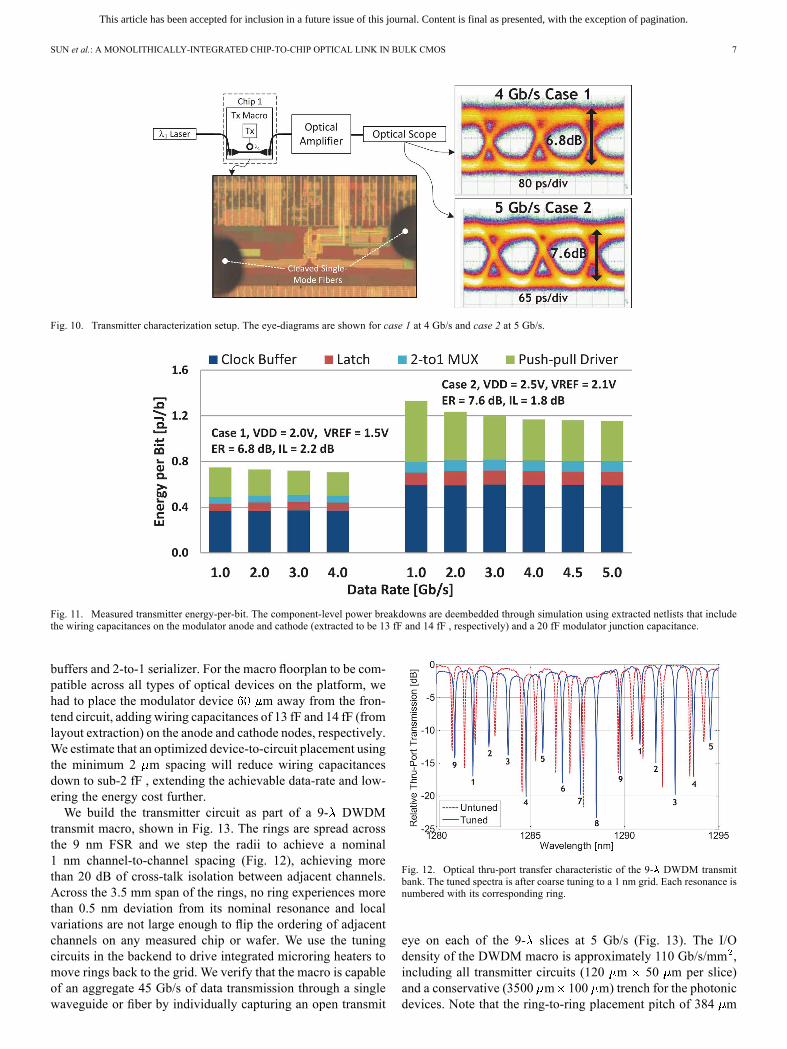
Fig. 10. Transmitter characterization setup. The eye-diagrams are shown for case 1 at 4 Gb/s and case 2 at 5 Gb/s.
Fig. 11. Measured transmitter energy-per-bit. The component-level power breakdowns are deembedded through simulation using extracted netlists that includethe wiring capacitances on the modulator anode and cathode (extracted to be 13 fF and 14 fF , respectively) and a 20 fF modulator junction capacitance.
buffers and 2-to-1 serializer. For the macro floorplan to be com-patible across all types of optical devices on the platform, wehad to place the modulator device m away from the fron-tend circuit, adding wiring capacitances of 13 fF and 14 fF (fromlayout extraction) on the anode and cathode nodes, respectively.We estimate that an optimized device-to-circuit placement usingthe minimum 2 m spacing will reduce wiring capacitancesdown to sub-2 fF , extending the achievable data-rate and low-ering the energy cost further.We build the transmitter circuit as part of a 9- DWDM
transmit macro, shown in Fig. 13. The rings are spread acrossthe 9 nm FSR and we step the radii to achieve a nominal1 nm channel-to-channel spacing (Fig. 12), achieving morethan 20 dB of cross-talk isolation between adjacent channels.Across the 3.5 mm span of the rings, no ring experiences morethan 0.5 nm deviation from its nominal resonance and localvariations are not large enough to flip the ordering of adjacentchannels on any measured chip or wafer. We use the tuningcircuits in the backend to drive integrated microring heaters tomove rings back to the grid. We verify that the macro is capableof an aggregate 45 Gb/s of data transmission through a singlewaveguide or fiber by individually capturing an open transmit
Fig. 12. Optical thru-port transfer characteristic of the 9- DWDM transmitbank. The tuned spectra is after coarse tuning to a 1 nm grid. Each resonance isnumbered with its corresponding ring.
eye on each of the 9- slices at 5 Gb/s (Fig. 13). The I/Odensity of the DWDM macro is approximately 110 Gb/s/mm ,including all transmitter circuits (120 m 50 m per slice)and a conservative (3500 m 100 m) trench for the photonicdevices. Note that the ring-to-ring placement pitch of 384 m

This article has been accepted for inclusion in a future issue of this journal. Content is final as presented, with the exception of pagination.
8 IEEE JOURNAL OF SOLID-STATE CIRCUITS, VOL. 50, NO. 4, APRIL 2015
Fig. 13. Demonstration of the 9- DWDM transmit macro. The double-edge transition in the eyes is due to the previous edge not fully settling after one bit-time.
Fig. 14. Optical micrograph and schematic of the receiver architecture.
and the overall size of DWDM macro (4000 m 900 m) islimited by the area of the digital testing backend; the pitch canbe as tight as 40 m without violating design rules.
V. POLYSILICON-BASED RESONANT OPTICAL RECEIVERThe receiver block is composed of a ring resonant defect-de-
tector connected to a receiver circuit, shown in Fig. 14. Tomitigate the slow speed of the process, we adopt a split-diodetechnique [23]; each PD microring is separated into twoelectrically-isolated PD-halves (PD-0, PD-1), each connectedto a receiver-half (RX-0/1) running at half-rate on oppositeclock phases. In effect, each receiver-half gets 1/2 of the totalphotocurrent , but is given twice the evaluation time.Each receiver-half circuit consists of an inverter-based TIAfollowed by a clocked sense-amplifier and RS latch. The TIAtransimpedance gain can be adjusted by configuring the feed-back resistor to be 12 k 4 k , or 12 k 4 k . Current andcapacitive DACs attached to the sense amplifier provide offsetcompensation and eye-measurement capability for the receiver.
We design the circuit to accommodate a potentially large darkcurrent range across all PD variants on the platform reticle;the dummy PDs and TIAs serve as dark current references,keeping the sense-amps balanced for large dark currents. Underextremely high dark currents, the current DAC at the input ofeach TIA cancels dark currents to keep the TIA biased in alinear regime. We note, however, that there is less than 50 pA ofdark current at a 10 V bias for the defect microring PD [33].Hence, the dark currents are low enough for the dark currentcancellation DAC and dummies to be removed in a receivertailored specifically for this device.A sense-amp undergoes two phases during evaluation time:
a linear integration phase in which is integrated onto thecap through the of the input transistor and an exponentialregeneration phase where the positive feedback of the cross-coupled inverters drives to the supply rails. The behaviorof the sense-amp can be modeled, to first-order, as:
(2)
This article has been accepted for inclusion in a future issue of this journal. Content is final as presented, with the exception of pagination.
SUN et al.: A MONOLITHICALLY-INTEGRATED CHIP-TO-CHIP OPTICAL LINK IN BULK CMOS 9
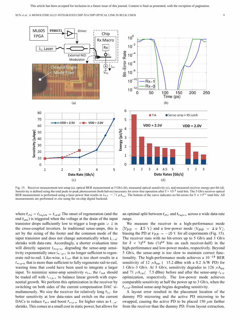
Fig. 15. Receiver measurement test setup (a), optical BER measurement at 5 Gb/s (b), measured optical sensitivity (c), and measured receiver energy-per-bit (d).Sensitivity is defined using the total peak-to-peak photocurrent (both halves) necessary for error-free operation after total bits. The 5 Gb/s receiver opticalBER measurement is performed using a laser power that results in A . The bottom of the curve indicates no bit-errors for total bits. Allmeasurements are performed in situ using the on-chip digital backend.
where The onset of regeneration (and theend ) is triggered when the voltage at the drain of the inputtransistor drops sufficiently low to trigger a loop-gain inthe cross-coupled inverters. In traditional sense-amps, this isset by the sizing of the footer and the common mode of theinput transistor and does not change automatically whenshrinks with data-rate. Accordingly, a shorter evaluation timewill directly squeeze , degrading the sense-amp sensi-tivity exponentially once is no longer sufficient to regen-erate rail-to-rail. Like-wise, a that is too short results in a
that is more than sufficient to fully regenerate rail-to-rail,wasting time that could have been used to integrate a largerinput. To minimize sense-amp sensitivity , the shouldbe traded off with to balance linear growth with expo-nential growth. We perform this optimization in the receiver byswitching on both sides of the current compensation DAC si-multaneously. We size the receiver for relatively long forbetter sensitivity at low data-rates and switch on the currentDACs to reduce and boost for higher rates asshrinks. This comes at a small cost in static power, but allows for
an optimal split between and across a wide data-raterange.We measure the receiver in a high-performance mode
and a low-power mode ,biasing the PD at for all experiments (Fig. 15).The receiver runs with no bit-errors up to 5 Gb/s and 3 Gb/sfor bits ( bits on each receiver-half) in thehigh-performance and low-power modes, respectively. Beyond5 Gb/s, the sense-amp is too slow to maintain correct func-tionality. The high-performance mode achieves a 10 BERsensitivity of 12 A ( 15.2 dBm with a 0.2 A/W PD) for1 Gb/s–3 Gb/s. At 5 Gb/s, sensitivity degrades to 126 Aand 71 A 7.5 dBm before and after the sense-ampoptimization, respectively. The low-power mode achievescomparable sensitivity at half the power up to 3 Gb/s, when the
-limited sense-amp begins degrading sensitivity.A layout error resulted in the placement location of the
dummy PD microring and the active PD microring to beswapped, causing the active PD to be placed 150 m fartherfrom the receiver than the dummy PD. From layout extraction,
This article has been accepted for inclusion in a future issue of this journal. Content is final as presented, with the exception of pagination.
10 IEEE JOURNAL OF SOLID-STATE CIRCUITS, VOL. 50, NO. 4, APRIL 2015
Fig. 16. Demonstration of the 9- DWDM receiver macro. The receive eye diagrams are generated by sweeping the receiver threshold using the offset compen-sation DACs.
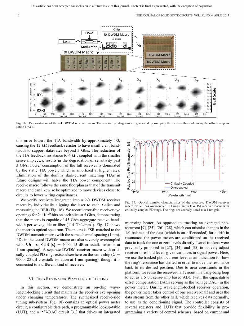
this error lowers the TIA bandwidth by approximately 1/3,causing the 12 k feedback resistor to have insufficient band-width to support data-rates beyond 3 Gb/s. The reduction ofthe TIA feedback resistance to 4 k , coupled with the smallersense-amp , results in the degradation of sensitivity past3 Gb/s. Power consumption of the full receiver is dominatedby the static TIA power, which is amortized at higher rates.Elimination of the dummy dark-current matching TIAs infuture designs will halve the TIA power component. Thereceive macro follows the same floorplan as that of the transmitmacro and can likewise be optimized to move devices closer tocircuits to lower wiring capacitances.We verify receivers integrated into a 9- DWDM receiver
macro by individually aligning the laser to each -slice andmeasuring the BER (Fig. 16). We record error-free receiver eyeopenings for bits on each slice at 5 Gb/s, demonstratingthat the macro is capable of 45 Gb/s aggregate receive band-width per waveguide or fiber (114 Gb/s/mm ). Fig. 17 showsthe macro's optical spectrum. The macro is FSR-matched to theDWDM transmit macro with the same channel spacing (1 nm).PDs in the tested DWDM macro are also severely overcoupledwith dB ( 4000, 15 dB crosstalk isolation at1 nm spacing). A separate DWDM receiver macro with criti-cally-coupled PD rings exists elsewhere on the same chip (9000, 23 dB crosstalk isolation at 1 nm spacing), though it isconnected to a different kind of receiver.
VI. RING RESONATOR WAVELENGTH LOCKING
In this section, we demonstrate an on-chip wave-length-locking circuit that maintains the receiver eye openingunder changing temperatures. The synthesized receive-sidetuning sub-system (Fig. 18) contains an optical power metercircuit, a configurable data path, a programmable lookup-table(LUT), and a -DAC circuit [31] that drives an integrated
Fig. 17. Optical transfer characteristics of the measured DWDM receivermacro, which has overcoupled PD rings, and a DWDM receiver macro withcritically-coupled PD rings. The rings are coarsely tuned to a 1 nm grid.
microring heater. As opposed to tracking an averaged pho-tocurrent [9], [25], [26], [28], which can mistake changes in the1/0-balance of the data (which is on-off encoded) for a drift inresonance, the power meters are conditioned on the receiveddata to track the one or zero levels directly. Level-trackers werepreviously proposed in [27], [34], and [35] to actively adjustreceiver threshold levels given variances in signal power. Here,we use the tracked photocurrent-level as an indication for howthe ring's resonance has drifted in order to move the resonanceback to its desired position. Due to area constraints in theplatform, we reuse the receiver-half circuit in a bang-bang loopto act as a 5 bit sense-amp based ADC (with the capacitativeoffset compensation DACs serving as the voltage DAC) in thepower meter. During wavelength-locked receiver operation,the power meter takes control of one receiver-half and uses thedata stream from the other half, which receives data normally,to use as the conditioning signal. The controller consists ofseveral registers and LUTs that provide flexibility in pro-gramming a variety of control schemes, based on current and

This article has been accepted for inclusion in a future issue of this journal. Content is final as presented, with the exception of pagination.
SUN et al.: A MONOLITHICALLY-INTEGRATED CHIP-TO-CHIP OPTICAL LINK IN BULK CMOS 11
Fig. 18. Architecture of the programmable tuning sub-system.
Fig. 19. Transient lock experiment with the tuning controller locked and without lock. The estimated temperature change is calculated from the aggressor powerprofile using 20 K/W and a time constant of 1s.
previous power meter outputs and arbitrary threshold values.The output of the controller is an 8-bit binary value for thethe heater strength. A -DAC (described in [31]) drives theintegrated heater. All tuning backend circuits are clocked bythe data-clock through a divide-by-64 divider.The lock range of the tuner is 0.5 nm (90 GHz) [36], cor-
responding to a 9 K change in temperature. In the context ofthe 9- transmit and receive DWDM macros, this range is mar-ginally sufficient to tune out local process mismatch but is stillless than the total desired (1.5 nm); applying the ring-to- as-signment shifting schemes from [19], the tuning range needs tobe around that of the channel spacing (1 nm) plus the worst-case local process variation (0.5 nm) to guarantee that each ringcan be assigned and tuned to a laser channel across all tem-peratures. Currently, the tuning range is limited by the max-imum heater output power of 6 mW (limited by the k re-sistance of the integrated heater and the 2.5 V supply). Thetuning range will increase by using a lower heater resistanceor by improving the tuning effiency, which we estimate to be67 W GHz 108 mW FSR . As a comparison point, a 3 mradius ring on the same platform with optimized heater place-ment demonstrated a tuning efficiency of 10 m GHz [31].
We perform a 2.5 Gb/s single-rate transient wavelength-lockexperiment, shown in Fig. 19. We clock-gate on/off the var-ious components in the digital backend of adjacent transceivermacros to create a temperature aggressor. These induce a mi-croring temperature change of approximately 20 K for everyWatt of power they dissipate. In this experiment, we program thecontroller with a simple tuning scheme where we simply heatmore if the power meter reading exceeds a set threshold and heatless if the readings are less. The wavelength-locked receiver iscompletely error-free until 65 seconds into the test, when weapply a deliberately large temperature change (approximately11 K) to exceed the lock range to force failure. By contrast, anunlocked receiver fails immediately with any temperature per-turbations caused by the aggressor due to a drop in photocurrentcaused by the drift in the ring's resonance. The tuning backendconsumes 0.43 mW at 2.5 Gb/s (171 fJ/bit) and 0.024 mm , ex-cluding the heater driver and the receiver. The area is largelydominated by the LUT and data-path and the tuning algorithmcan also be synthesized directly into gates at design time to con-serve power and area.

This article has been accepted for inclusion in a future issue of this journal. Content is final as presented, with the exception of pagination.
12 IEEE JOURNAL OF SOLID-STATE CIRCUITS, VOL. 50, NO. 4, APRIL 2015
Fig. 20. Chip-to-chip optical link across the room (a), 2 Gb/s (b) and 5 Gb/s (c) link BERmeasurements for bits, and estimated optical power breakdownsof the 2 Gb/s and 5 Gb/s chip-to-link links (d).
VII. MONOLITHIC CHIP-TO-CHIP LINK IN BULK
Using the transceiver macros, we build a chip-to-chip opticallink through 5 m of single-mode fiber interconnecting the two
chips (Fig. 20). We note that this demonstration uses a singleand clocks are forwarded to both chips electrically. Normally,in a DWDM configuration with multiple , the clock wouldbe available as a transmit-forwarded signal on one of the other

This article has been accepted for inclusion in a future issue of this journal. Content is final as presented, with the exception of pagination.
SUN et al.: A MONOLITHICALLY-INTEGRATED CHIP-TO-CHIP OPTICAL LINK IN BULK CMOS 13
Fig. 21. Link power analysis across data-rates using the current set of devices placed in the transmit/receive macros and if the best-known measured devices areplaced into the transmit/receive macros.
wavelengths. We demonstrate a full-rate 2 Gb/s chip-to-chiplink that is error-free for bits. Themaximum data-rate ofthe link is currently limited by the degradation of receiver sen-sitivity at higher rates and the 10 mW maximum output powerof the off-chip laser. We currently hit this limit due to an extra9 dB of optical loss caused by a sub-optimal permutation of op-tical devices in the transceiver macros; VGCs in the transceivermacros contribute 5 dB of loss per coupler, compared to the 3 dBloss VGCs present elsewhere on the platform. Additionally, theseverely overcoupled photodetector rings (2.4 dB ER ) effec-tively results in another loss of 3.7 dB. To overcome the losswith the current combination of devices, we insert an opticalamplifier between the transmit chip and the receive chip, whichadds approximately 8 dB of optical gain and enables 5 Gb/s op-eration for the link. The link consumes 4 pJ/b electrical and5 pJ/b optical energy at 2 Gb/s. At 5 Gb/s, the link consumes3 pJ/b electrical and 12 pJ/b optical energy.We perform a link power analysis across a range of data-rates
using the metrics from the measured circuits (Fig. 21). We cal-culate the wall-plug laser power of the link as
(3)
where is the laser wall-plug efficiency, is the receiversensivity (in ), is the photodetector responsivity,is the modulator extinction ratio and is the total opticalloss in the path from the laser to receiver. For this analysis,we assume an 25%. We show a case using devices cur-rently in the transceiver macros and a case using best-known de-vices on the current platform. In both cases, the link is most en-ergy-efficient at a data-rate of 3 Gb/s–4 Gb/s. Static power (mi-croring heating/tuning, receiver TIA, the receiver) is amortizedat higher rates. Energy-per-bit from the laser also decreases ini-tially from 1 Gb/s–3 Gb/s, where (and hence ) remainsflat. At the higher rates, increases drastically and offsets the
energy-per-bit improvement from the higher data-rate. For thecase using the current set of devices in the transceiver macros,the laser wallplug power dominates the energy-per-bit, reachingan optimal wall-plug link energy of 18.3 pJ/b at 3 Gb/s. In thesecond case, the better devices reduce optical loss by more than9 dB. As such, the laser is no longer dominant for 1 Gb/s–4 Gb/sand an optimal energy efficiency of 6.5 pJ/b is reached at 4 Gb/s.
VIII. CONCLUSION
To facilitate the adoption of photonics for mainstream CMOSapplications, we must first remove its intimidation factor: provethat the technology is viable for electronics integration withoutexotic processing steps, customized SOI wafers, or complicatedpackaging. To this end, we demonstrate a polysilicon-onlymonolithic photonics platform in bulk CMOS, to show thatlow-loss waveguides and active optical structures can be in-tegrated through a minimal number of process changes. Byavoiding epitaxially grown crystalline silicon for waveguidesand finding an alternative to germanium integration for pho-todetectors, the polysilicon-only photonics module minimizesrisks to process-native transistors and improves technologyportability.We build a portfolio of DWDM link components-a DWDM
transmitter and a DWDM receiver-each demonstrating com-petitive performance and efficiency despite the early stage ofplatform development. We further improve the robustness ofthe wavelength-locking techniques by resolving the data-depen-dency challenge, demonstrating that robust DWDM ring tuningis feasible in a hostile temperature environment. We composean optical chip-to-link, which, to the knowledge of the authors,is the first demonstration of a monolithically-integrated opticallink in a bulk CMOS process. The unique polysilicon aspectsof this photonic platform make it independent of the front-endintegration processes, enabling deployment in more advanced
This article has been accepted for inclusion in a future issue of this journal. Content is final as presented, with the exception of pagination.
14 IEEE JOURNAL OF SOLID-STATE CIRCUITS, VOL. 50, NO. 4, APRIL 2015
bulk CMOS process nodes to further scale the link performanceand energy efficiency.
ACKNOWLEDGMENT
The authors gratefully acknowledge the help and supportfrom all POEM team members at Micron Technology Inc.,MIT, CU Boulder, and UC Berkeley.
REFERENCES[1] I. Young et al., “Optical I/O technology for tera-scale computing,”
IEEE J. Solid-State Circuits, vol. 45, no. 1, pp. 235–248, Jan. 2010.[2] S. Beamer et al., “Re-architecting DRAMmemory systemswith mono-
lithically integrated silicon photonics,” in Proc. 37th Annu. ACM Int.Symp. Comput. Architecture, ISCA'10, 2010, pp. 129–140.
[3] N. Binkert et al., “The role of optics in future high radix switch design,”in Proc. 38th Annu. ACM Int. Symp. Comput. Architecture, ISCA'11,2011, pp. 437–448.
[4] S. Assefa et al., “A 90 nm CMOS integrated nano-photonics tech-nology for 25 Gbps WDM optical communications applications,” in2012 IEEE Int. Electron Devices Meeting (IEDM), 2012, pp. 33.8.1–33.8.3.
[5] J. Li, G. Li, X. Zheng, K. Raj, A. Krishnamoorthy, and J. Buckwalter,“A 25-Gb/s monolithic optical transmitter with micro-ring modulatorin 130-nm SoI CMOS,” IEEE Photonics Technol. Lett., vol. 25, no. 19,pp. 1901–1903, Oct. 2013.
[6] M. Georgas et al., “A monolithically-integrated optical transmitter andreceiver in a zero-change 45 nm SOI process,” in 2014 Symp. VLSICircuits Dig. Tech. Papers, 2014, pp. 58–59.
[7] H. Byun et al., “Bulk-Si photonics technology for DRAM interface,”Photon. Res., vol. 2, no. 3, pp. A25–A33, Jun. 2014.
[8] X. Zheng et al., “2-pJ/bit (on-chip) 10-Gb/s digital CMOS siliconphotonic link,” IEEE Photon. Technol. Lett., vol. 24, no. 14, pp.1260–1262, Jul. 2012.
[9] C. Li et al., “Silicon photonic transceiver circuits with microring res-onator bias-based wavelength stabilization in 65 nm CMOS,” IEEE J.Solid-State Circuits, vol. 49, no. 6, pp. 1419–1436, Jun. 2014.
[10] M. Nazari and A. Emami-Neyestanak, “A 24-Gb/s double-samplingreceiver for ultra-low-power optical communication,” IEEE J. Solid-State Circuits, vol. 48, no. 2, pp. 344–357, Feb. 2013.
[11] J.-S. Kim et al., “A 1.2 V 12.8 GB/s 2Gb mobile wide-I/O DRAMwith 4x128 I/os using TSV-based stacking,” in IEEE Int. Solid-StateCircuits Conf. (ISSCC) Dig. Tech. Papers, 2011, pp. 496–498.
[12] M. Wordeman, J. Silberman, G. Maier, and M. Scheuermann, “A 3Dsystem prototype of an eDRAM cache stacked over processor-likelogic using through-silicon vias,” in IEEE Int. Solid-State CircuitsConf. (ISSCC) Dig. Tech. Papers, 2012, pp. 186–187.
[13] J. Buckwalter, X. Zheng, G. Li, K. Raj, and A. Krishnamoorthy, “Amonolithic 25-Gb/s transceiver with photonic ring modulators and gedetectors in a 130-nm CMOS SOI process,” IEEE J. Solid-State Cir-cuits, vol. 47, no. 6, pp. 1309–1322, Jun. 2012.
[14] J. S. Orcutt et al., “Open foundry platform for high-performanceelectronic-photonic integration,” Opt. Express, vol. 20, no. 11, pp.12,222–12,232, May 2012.
[15] B. Moss et al., “A 1.23 pJ/b 2.5 Gb/s monolithically integrated opticalcarrier-injection ring modulator and all-digital driver circuit in com-mercial 45 nm SOI,” in IEEE Int. Solid-State Circuits Conf. (ISSCC)Dig. Tech. Papers, 2013, pp. 126–127.
[16] M. T. Wade et al., “Energy-efficient active photonics in a zero-change,state-of-the-art CMOS process,” in Opt. Fiber Commun. Conf. Opt.Soc. Am., 2014, p. Tu2E.7.
[17] J. S. Orcutt et al., “Nanophotonic integration in state-of-the-art CMOSfoundries,” Opt. Express, vol. 19, no. 3, pp. 2335–2346, Jan. 2011.
[18] R. Meade et al., “Integration of silicon photonics in a bulk CMOSmemory flow,” in 2013 IEEE Opt. Interconnects Conf., 2013, pp.114–115.
[19] M. Georgas, J. Leu, B. Moss, C. Sun, and V. Stojanovic, “Addressinglink-level design tradeoffs for integrated photonic interconnects,” inProc. IEEE Custom Integrated Circuits Conf. (CICC), 2011, pp. 1–8.
[20] J. Leu and V. Stojanovic, “Injection-locked clock receiver for mono-lithic optical link in 45 nm SOI,” in Proc. IEEE Asian Solid State Cir-cuits Conf. (A-SSCC), 2011, pp. 149–152.
[21] R. Soref and B. Bennett, “Electrooptical effects in silicon,” IEEE J.Quantum Electron., vol. 23, no. 1, Jan. 1987.
[22] Q. Xu, S. Manipatruni, B. Schmidt, J. Shakya, and M. Lipson, “12.5Gbit/s carrier-injection-based silicon micro-ring silicon modulators,”Opt. Soc. Am., vol. 15, no. 2, Jan. 2007.
[23] M. Georgas, J. Orcutt, R. Ram, and V. Stojanovic, “A monolithically-integrated optical receiver in standard 45-nm SOI,” IEEE J. Solid-StateCircuits, vol. 47, no. 7, pp. 1693–1702, Jul. 2012.
[24] S. Selvaraja, W. Bogaerts, D. V. Thourhout, and R. Baets, “Fabricationof uniform photonic devices using 193 nm optical lithography in sil-icon-on-insulator,” in Proc. 14th Eur. Conf. Integr. Opt. (ECIO), 2008.
[25] K. Padmaraju, J. Chan, L. Chen, M. Lipson, and K. Bergman, “Thermalstabilization of a microring modulator using feedback control,” Opt.Express, vol. 20, no. 27, pp. 27,999–28,008, Dec. 2012.
[26] E. Timurdogan et al., “Automated wavelength recovery for microringresonators,” in Proc. Conf. Lasers Electro-Optics Opt. Soc. Am., 2012,p. CM2M 1.
[27] P. Amberg et al., “A sub-400 fj/bit thermal tuner for optical resonantring modulators in 40 nm CMOS,” in Proc. IEEE Asian Solid StateCircuits Conf. (A-SSCC), 2012, pp. 29–32.
[28] X. Zheng et al., “A high-speed, tunable silicon photonic ring mod-ulator integrated with ultra-efficient active wavelength control,” Opt.Express, vol. 22, no. 10, pp. 12,628–12,633, May 2014.
[29] R. Meade et al., “Integration of silicon photonics in bulk CMOS,” inSymp. VLSI Technol. Dig. Tech. Papers, 2014, pp. 228–229.
[30] H.-C. Ji et al., “Optical interface platform for DRAM integration,” inOpt. Fiber Commun. Conf. and Exposition (OFC/NFOEC), 2011 andthe Nat. Fiber Optic Engineers Conf., 2011, pp. 1–3.
[31] C. Sun, E. Timurdogan, M. Watts, and V. Stojanovic, “Integrated mi-croring tuning in deep-trench bulk CMOS,” in Proc. IEEE Opt. Inter-connects Conf., 2013, pp. 54–55.
[32] S. Assefa, W. Green, A. Rylyakov, C. Schow, F. Horst, and Y. Vlasov,“Monolithic integration of silicon nanophotonics with CMOS,” inProc. IEEE Photonics Conf. (IPC), 2012, pp. 626–627.
[33] K. K. Mehta et al., “Polycrystalline silicon ring resonator photodiodesin a bulk complementary metal-oxide-semiconductor process,” Opt.Lett., vol. 39, no. 4, pp. 1061–1064, Feb. 2014.
[34] E. Chang, F. Liu, P. Amberg, J. Lexau, and Ho, “Efficient techniquesfor canceling transceiver noise,” in Proc. Int. Symp. VLSI Design, Au-tomation, and Test (VLSI-DAT), 2013, pp. 1–4.
[35] V. Stojanovic et al., “Autonomous dual-mode (PAM2/4) serial linktransceiver with adaptive equalization and data recovery,” IEEE J.Solid-State Circuits, vol. 40, no. 4, pp. 1012–1026, Apr. 2005.
[36] C. Sun et al., “A monolithically-integrated chip-to-chip optical linkin bulk CMOS,” in Symp. VLSI Circuits Dig. Tech. Papers, 2014, pp.56–57.
Chen Sun (S’09) received the B.S. degree in elec-trical engineering and computer science from theUniversity of California, Berkeley, CA, USA, in2009, and the S.M. degree in electrical engineeringin 2011 from the Massachusetts Institute of Tech-nology, Cambridge, MA, USA, where he is currentlya Ph.D. candidate.He held internships at Nvidia in 2008 and 2009
and at Rambus in 2010. Since 2013, he has been avisiting student at the Berkeley Wireless ResearchCenter, focusing on system-level integration of sil-
icon-photonics. His research interests include design of energy efficient inter-connects, modeling and implementation of electro-optic devices and systems,and techniques for dense wavelength-division multiplexed (DWDM) opticaltransceivers.
Michael Georgas (S’07–M’13) received theB.A.Sc. in engineering science from the Universityof Toronto, Toronto, ON, Canada, in 2007, theMaster degree from the Massachusetts Institute ofTechnology (MIT), Cambridge, MA, USA, in 2009,and the Ph.D. in electrical engineering and computerscience from MIT in 2013.He completed a Postdoctoral Associate position in
the Research Lab of Electronics Translational Fel-lows Program at MIT. His research interests lie inthe field of integrated photonics and high-speed links,
andmore recently the application and commercialization of integrated photonicsin data-centers.

This article has been accepted for inclusion in a future issue of this journal. Content is final as presented, with the exception of pagination.
SUN et al.: A MONOLITHICALLY-INTEGRATED CHIP-TO-CHIP OPTICAL LINK IN BULK CMOS 15
Jason S. Orcutt received the B.S. degree in electricalengineering from Columbia University, New York,NY, USA, in 2005, and the M.S. and Ph.D. degrees inelectrical engineering and computer science from theMassachusetts Institute of Technology (MIT), Cam-bridge, MA, USA, in 2008 and 2012, respectively.From 2012 to 2013, he worked as a research sci-
entist at MIT. Since 2013, he has been a researchstaff member in the Physical Sciences department ofIBM's T. J. Watson Research Center. His research in-terests range from ultrafast and integrated optics to
bioelectronics and stochastic systems.Dr. Orcutt was the recipient of a National Sciences Foundation Graduate Re-
search Fellowship from 2005 to 2008.
Benjamin Moss (S’07–M’08) received the B.S.degrees from the Missouri University of Scienceand Technology, Rolla, MO, USA, in 2006, the M.S.degree in electrical engineering and computer sci-ence from the Massachusetts Institute of Technology(MIT), Cambridge, MA, USA, in 2009, and thePh.D. degree in electrical engineering and computerscience from MIT in 2014.He is interested in the applications of high-speed
photonic interconnects in industry applications
Yu-Hsin Chen (S'11) received the B.S. degree inelectrical engineering from National Taiwan Univer-sity, Taipei, Taiwan, in 2009, and the S.M. degree inelectrical engineering and computer science from theMassachusetts Institute of Technology, Cambridge,MA, USA, in 2013, where he is currently workingtoward the Ph.D. degree.His research focuses on energy-efficient algorithm,
architecture, and VLSI design for computer architec-ture and computer vision systems.
Jeffrey M. Shainline received the B.S. degree inphysics from the University of Colorado, Boulder,CO, USA, in 2005, and the Ph.D. degree from BrownUniversity, Providence, RI, USA, in 2010.From 2010 to 2013, he was a postdoctoral re-
searcher in the laboratory of Dr. Miloš Popović atthe University of Colorado. In 2013, he joined theDivision of Optoelectronics and Photonics at theNational Institute of Standards and Technology inBoulder, Colorado as a National Research CouncilPostdoctoral Fellow. His work concerns the integra-
tion of chipscale quantum photonic devices with superconducting single-photondetectors.
Mark Wade received the B.S. degrees in electricalengineering and physics from Louisiana Tech Uni-versity, Ruston, LA, USA, in 2010, and the M.S. de-gree in electrical engineering from the University ofColorado, Boulder, CO, USA, in 2013. He is a Ph.D.candidate in Dr. Miloš Popović's group at the Univer-sity of Colorado Boulder and a Research Affiliate atMIT in Prof. Rajeev Ram's group.He was a NIST Measurement, Science and Engi-
neering Fellow and is currently a National ScienceFoundation Graduate Research Fellow. In his grad-
uate work, he has focused on realizing high performance photonic devices inadvanced CMOS processes which include efficient photonic filters, optical mod-ulators, grating couplers, and detectors. His interests are in using photonic/elec-tronic integration to create efficient communication links.
Karan Mehta received the B.S. degrees in electricalengineering and physics from the University ofCalifornia at Los Angeles (UCLA), CA, USA, in2010, and the S.M. in electrical engineering andcomputer science from the Massachusetts Instituteof Technology, Cambridge, MA, USA, in 2012. Heis currently pursuing research in integrated opticsfor trapped ion quantum systems.
Kareem Nammari received the M.S. degree in 2014and the B.S. degree in 2012 in electrical engineeringfrom the University of Colorado, Boulder, CO, USA.He was an M.S. student in Dr. Miloš Popović's groupat the University of Colorado Boulder. His graduatework focused on energy-efficient grating couplers inadvanced CMOS processes.His interests include optical-electrical intercon-
nects and swept wavelength sources. He is currentlyemployed with Insight Photonic Solutions.
Erman Timurdogan (S’13) received the B.S.(Hons.) degree in electrical and electronics engi-neering from Koc University, Istanbul, Turkey, in2010. He then joined the Photonics MicrosystemsGroup, the Massachusetts Institute of Technology(MIT), Cambridge, MA, USA. He received theS.M. degree in electrical engineering from MITin 2013 in “automated wavelength recovery forsilicon photonics.” He is currently a member of thePhotonics Microsystems Group at MIT and workingtoward the Ph.D. degree.
He was with Mercedes-Benz Turk, Istanbul, Turkey, in 2008 and Bruker Op-tics, Karlsruhe, Germany, in 2009. His current research interests include mod-eling and testing integrated electro-optic and thermo-optic photonic devices andsystems for low-power, high speed, wavelength division multiplexed (WDM)communications. He has more than 35 authored and coauthored conference andjournal publications and an issued patent.Mr. Timurdogan is a member of the Optical Society of America (OSA).
Daniel L. Miller holds a Ph.D. in TheoreticalPhysics from the Hebrew University in Jerusalem.He worked in the Weizmann Institute of Sciencefrom 1996 to 1999 in the field of quantum chaos.In 1999, he joined Intel and worked for 10 yearsas a device engineer on sustaining and developingnumerous technologies. He joined Micron Israel in2010, working in R&D on 45 nm NOR devices andlater on silicon photonics. In 2014, he returned toIntel and is currently working on 14 nm productdevelopment.
Ofer Tehar-Zehav worked for Intel and Numonyxon 45 nm NOR process integration, before joiningMicron Technology. While at Micron, he integratedsilicon photonics process modules covered in thiswork. In 2013, he returned to Intel in Haifa, Israel.

This article has been accepted for inclusion in a future issue of this journal. Content is final as presented, with the exception of pagination.
16 IEEE JOURNAL OF SOLID-STATE CIRCUITS, VOL. 50, NO. 4, APRIL 2015
Zvi Sternberg worked for Intel and Numonyx on 45nm NOR process integration, before joining MicronTechnology. While at Micron, he was an engineeringmanager for process integration, contributing to thedevelopment of silicon photonics process modules.
Jonathan Leu was born in Columbia, SC, USA, andgrew up in Michigan, USA, and Hsinchu, Taiwan.He received the Bachelor degree in 2007 from Na-tional Chiao Tung University, Hsinchu, Taiwan, andthe Master degree in 2010, both in electrical engi-neering and computer science.His interests are focused on novel integrated pho-
tonic timing circuits, and developing simulation toolsthat are CMOS compatable.
Johanna Chong received the B.S. degree in electrical engineering from theMassachusetts Institute of Technology (MIT), Cambridge, MA, USA, in 2012.She received the M.Eng. degree in electrical engineering in February 2014 fromMIT, having completed her thesis on hybrid-CMOS based multiwavelengthlasers.She is an R&D Electronics Engineer at Sandia National Laboratory, Albu-
querque, NM, USA, where she works on embedded systems.
Reha Bafrali received the B.S. degree in chemicalengineering from Carnegie-Mellon University,Pittsburgh, PA, USA, in 1984, and the Ph.D. degreein chemical engineering from the University ofCalifornia, Berkeley, CA, USA, in 1995.He worked for Intel Corporation from 1995 to
2008, initially as a process engineer on wafer cleansand photolithography before making the transition todeveloping models and recipes for optical proximitycorrection (OPC) in 1999. He joined Numonyx BVat its formation in 2008 and Micron in 2010 as part
of the acquisition of Numonyx.
Gurtej S. Sandhu (M’91–SM’06–F’11) received thedegree in electrical engineering from the Indian Insti-tute of Technology, New Delhi, India, and the Ph.D.degree in physics from the University of North Car-olina, Chapel Hill, NC, USA, in 1990.He is Senior Fellow and Director of Advanced
Technologies Research at Micron Technology Inc.In his current role, he manages the AdvancedMemory Materials and Technologies research anddevelopments at Micron. At Micron he has servedin a variety of engineering and management roles
responsible for process technology development, pilot manufacturing andtransfers to manufacturing. He has been actively involved with a broad rangeof process technologies for making computer chips. He has been associatedwith microelectronics technology for over 24 years and has pioneered severaltechnologies which are currently employed in mainstream chip manufacturing.More recently, he was involved with introduction of a number of Atomic LayerDeposition (ALD) based processes and innovative patterning techniques formemory chip technology used by all major chip manufacturing companiesaround the world.
Dr. Sandhu has served as a guest speaker at numerous international events,authored many technical papers and holds over 1100 issued U.S. patents. Hehas received several honors and recognition for these contributions from inter-national technical societies and organizations. Dr. Sandhu is a Fellow of IEEE.
Michael R. Watts (M’10) is a principal investigatorin the Research Laboratory of Electronics (RLE) anda member of the Electrical Engineering and Com-puter Science Department (EECS) at the Massachu-setts Institute of Technology. He received his Bach-elor of Science in Electrical Engineering from TuftsUniversity in 1996. He then joined Draper Labora-tory as aMember of Technical Staff in their Fiber Op-tics Group. In 1999 he became a Draper Fellow andreceived his SM and PhD degrees from MIT in 2001and 2005, respectively. In 2005 he joined Sandia Na-
tional Labs where he led their silicon photonics effort as a Principal Member ofTechnical Staff. In 2010 he returned to MIT as an Associate Professor.Prof. Watts' research focuses on photonic microsystems for low-power com-
munications, sensing, and microwave-photonics applications. His current inter-ests include the modeling, fabrication, and testing of large-scale implementa-tions of microphotonic circuits, systems, and networks that are being integrated,directly or through hybrid techniques, with CMOS electronics for high-speedtransmitting, switching, and routing applications of digital signals. Additionalinterests include large-scale microphotonic sensing and imaging arrays, alongwith optical phased arrays, nanophotonic antennas, nonlinear optics, and ma-nipulations of optical-electromagnetic fields on-chip.
Roy Meade (M’98–SM’09) holds the BME andMSME from the Georgia Institute of Technology,Atlanta, GA, USA, and the MBA from Duke Uni-versity, Durham, NC, USA, graduating as a FuquaScholar.He is a Senior Member of Technical Staff and
a Senior Program Manager for High BandwidthMemory at Micron Technology, Inc. He is also theprogram manager for Micron's POEM Program, aDARPA funded silicon photonics collaboration withMIT, UC Berkeley, and UC Boulder. He has over 15
years in CMOS manufacturing and R&D spanning ASIC, DRAM, resistiveRAM, and photonics. His research interests include the material science anddevice physics of beyond CMOS devices as well as silicon photonic devicefabrication. He is a Senior Member of the IEEE, and has 25 US patents.
Miloš Popović (S’98–M’05) was born in Zajecar,Serbia (formerly Yugoslavia), in 1977. He receivedthe B.Sc.E. degree in electrical engineering fromQueen's University, Kingston, ON, Canada, in1999, and the M.S. and Ph.D. degrees in electricalengineering from the Massachusetts Institute ofTechnology (MIT), Cambridge, MA, USA, in 2002and 2008, respectively.Since 2010, he has been an Assistant Professor in
the Department of Electrical, Computer and EnergyEngineering, University of Colorado, Boulder, CO,
USA. In 2012, he was named a Fellow of the David & Lucile Packard Founda-tion. His research interests include silicon photonic circuits, CMOS photonicsintegration and optical interconnects, nonlinear and quantum integrated pho-tonics, and light-forces based, nanomechanical photonic devices. More gener-ally, his interests are in the application of electromagnetic theory and solid-statephysics toward the invention of devices that function based on novel aspects ofthe physics of light-matter interaction. He is also interested in electromagnetictheory and numerical methods related to photonics.Dr. Popović has served on the technical program committees for the Op-
tical Fiber Communication conference (OFC), the Conference on Lasers andElectro-Optics (CLEO), Integrated Photonics Research (IPR) and Group IVPhotonics (GFP). He is an inventor or co-inventor on over 16 patents, and au-thor or co-author of over 130 research papers and two book chapters.

This article has been accepted for inclusion in a future issue of this journal. Content is final as presented, with the exception of pagination.
SUN et al.: A MONOLITHICALLY-INTEGRATED CHIP-TO-CHIP OPTICAL LINK IN BULK CMOS 17
Rajeev J. Ram (S’94–M’96–SM’07) received theB.S. degree in applied physics from the CaliforniaInstitute of Technology, Pasadena, CA, USA, in1991, and the Ph.D. degree in electrical engineeringfrom the University of California, Santa Barbara,CA, USA, in 1997.He is currently a Professor at the Massachusetts
Institute of Technology, Cambridge, MA, USA. Hisresearch focuses on physical optics and electronics,including the development of novel components andsystems for communications and sensing and studies
of fundamental interactions between electronic materials and light.
Vladimir Stojanović (S’96–M’04) received theDipl. Ing. degree from the University of Belgrade,Serbia, in 1998, and the Ph.D. in electrical engi-neering from Stanford University, Stanford, CA,USA, in 2005.He is an Associate Professor of electrical engi-
neering and computer science at the University ofCalifornia, Berkeley, CA, USA. His research inter-ests include design, modeling and optimization ofintegrated systems, from CMOS-based VLSI blocksand interfaces to system design with emerging
devices like NEM relays and silicon-photonics. He is also interested in designand implementation of energy-efficient electrical and optical networks, anddigital communication techniques in high-speed interfaces and high-speedmixed-signal IC design. He was also with Rambus, Inc., Los Altos, CA, USA,as a Principal Engineer from 2001 through 2004, and with MIT as an AssociateProfessor from 2005 to 2013.Dr. Stojanović received the 2006 IBM Faculty Partnership Award, and the
2009 NSF CAREER Award, as well as the 2008 ICCAD William J. McCalla,2008 IEEE TRANSACTIONS ON ADVANCED PACKAGING, and 2010 ISSCC JackRaper Best Paper Awards. He was an IEEE Solid-State Circuits Society Distin-guished Lecturer for the 2012–2013 term.


![I,'plab.colorado.edu/pubs_pdfs/c47.pdf · In the first part of this paper (Sec. 2), we show [1] how practical devices realizing these capabilities may be designed, and explain the](https://img.dokumen.tips/doc/110x75/5b5e56197f8b9aa3048cce9e/iplab-in-the-first-part-of-this-paper-sec-2-we-show-1-how-practical.jpg)