Embed Size (px)
Citation preview
Finite-difference complex-wavevector band structuresolver for analysis and design
of periodic radiative microphotonic structuresJelena Notaros and Miloš A. Popović*
Department of Electrical, Computer, and Energy Engineering, University of Colorado, Boulder, Colorado 80309, USA*Corresponding author: [email protected]
Received January 26, 2015; accepted February 2, 2015;posted February 6, 2015 (Doc. ID 232985); published March 11, 2015
We demonstrate a finite-difference approach to complex-wavevector band structure simulation and its use as a toolfor the analysis and design of periodic leaky-wave photonic devices. With the (usually real) operating frequency andunit-cell refractive index distribution as inputs, the eigenvalue problem yields the complex-wavevector eigenvaluesand Blochmodes of the simulated structure. In a two-dimensional implementation for transverse-electric fields withradiation accounted for by perfectly matched layer boundaries, we validate the method and demonstrate its use insimulating the complex-wavevector band structures and modal properties of a silicon photonic crystal waveguide,an array-antenna-inspired grating coupler with unidirectional radiation, and a recently demonstrated low-lossBloch-mode-based waveguide crossing array. Additionally, we show the first direct solution of the recently pro-posed open-system low-loss Blochmodes.We expect this method to be a valuable tool in photonics design, enablingthe rigorous analysis and synthesis of advanced periodic and quasi-periodic photonic devices. © 2015 OpticalSociety of AmericaOCIS codes: (050.1755) Computational electromagnetic methods; (130.3120) Integrated optics devices; (130.5296)
Photonic crystal waveguides; (050.6624) Subwavelength structures.http://dx.doi.org/10.1364/OL.40.001053
Periodic structures, such as photonic crystal microcav-ities and waveguides [1], fiber-to-chip grating couplers[2,3], and waveguide crossing arrays [4,5], are playingan increasingly important role in the design of integratedphotonic circuits. With the prospect that silicon photon-ics can enable significant advances in a number of appli-cations, including energy efficient processor-to-memoryinterconnects [6] and optical phased arrays [7], there is aneed for efficient techniques for the rigorous design ofperiodic micro- and nanophotonic structures.A natural way to design periodic photonic structures is
through band structure analysis, i.e., Bloch–Floquettheory, using numerical solvers [8]. This approach allowsrapid efficient design of most of the properties of a peri-odic structure through the design of a single unit cell.Since photonic band solvers typically take as input a realwavevector, k, absorbing or radiating structures are typ-ically described by a computed complex-frequency andare effectively seen as a finite-quality-factor resonator.Furthermore, these solvers are unable to readily provideband structure information within bandgaps where themost natural picture involves a complex-wavevector;yet these bandgap fields are critical to the design of struc-tures such as photonic crystal microcavities [1].For devices designed to operate at a particular real
driving frequency, complex-wavevector band structureanalysis, with driving frequency provided at input, isthe natural basis for physical intuition and rigorous analy-sis [9]. This is particularly true for propagation within thebandgaps of lossless structures (which do not appear inreal-wavevector complex-frequency analysis) and for ab-sorbing and leaky-wave radiative structures. For example,the optimization of grating couplers based on antenna-array concepts [3] implies a fixed real design frequencyand optimization for radiation angle and decay rate—bothcomputed from the complex-wavevector.
Furthermore, in our view, the complex-wavevectorband structure picture could be particularly importantfor the design and synthesis of advanced “tapered-band-structure” devices, where unit cells with varyingparameters are concatenated, all designed at a fixed realfrequency of interest, to form a final device design. Suchquasi-periodic structures with adiabatic tapering of theunit cell [10] have been employed to engineer high-quality-factor photonic crystal microcavities [1] andhigh-efficiency grating couplers [2]. Yet, their design hastypically involved less than ideally suited tools such asfinite-difference time-domain (FDTD) simulation or indi-rect complex-frequency band structure methods withanalytical approximations in bandgaps [1]. Rigorous syn-thesis techniques are lacking, and band structure analysisappears to be inadequately adapted to date to these kindsof photonics design problems.
Recent work has investigated complex-wavevectorband structure calculation in the context of modelingplasmonic/polaritonic structures to account for materialabsorption [11–14], as well as radiation loss through theincorporation of absorbing domain terminations such asperfectly matched layers [15].
In this Letter, we demonstrate a novel finite-differencecomplex-wavevector band structure solver with per-fectly-matched-layer (PML) absorbing boundaries. Weuse the solver to compute the modal properties oftwo-dimensional radiating periodic photonic structuresand suggest a vision for rigorous device synthesis basedon such solvers. By utilizing a finite-difference method ona split Yee grid, our solver is robust since it is derivedfrom self-consistent discrete electromagnetism withdiscrete conservation laws [16], enabling a completeorthogonal basis with no spurious solutions in the formu-lation. Furthermore, the solver’s uniform grid allowsfor accurate simulation of coupled resonator physics
March 15, 2015 / Vol. 40, No. 6 / OPTICS LETTERS 1053
0146-9592/15/061053-04$15.00/0 © 2015 Optical Society of America

due to its consistent discretization of identical elementsin the computational domain. This approach also makesthe band structure solver directly integrable with FDTDand finite-difference waveguide mode solvers.We first present the complex-wavevector electromag-
netic eigenvalue problem formulation and implementa-tion of the solver with PML boundary conditions andfollow with validation of the method against an analyticalsolution. Next, we analyze the modal properties and bandstructures of a silicon linear photonic crystal waveguide,a unidirectional antenna-array-inspired fiber-to-chip gra-ting coupler [3], and a low-loss Bloch-mode waveguidecrossing array, where we demonstrate the first directsolution of the recently proposed open-system low-lossBloch modes [4,5]. These examples illustrate the poten-tial utility of a complex-wavevector band structure solverin device design.Starting from Maxwell’s equations, we derive the wave
equation for the transverse electric field, Ψ�x; y�, of atwo-dimensional structure,
�∂2x � ∂2y � k20n2�x; y��Ψ�x; y� � 0; (1)
where k0 ≡ 2πf∕c ≡ 2π∕λ0 is the free-space wavenumber(related to wavelength, λ0, and frequency, f ) and n�x; y�is the refractive index distribution of the structure.Notably, in our implementation, the refractive indexmay be real or complex, enabling simulation of dielectric,plasmonic, and other structures. For an index distribu-tion that is periodic along x with periodicity a such thatn�x; y� � n�x� a; y�, Bloch’s theorem states that thefield within the periodic medium can be representedas the product of an amplitude function periodic in xwiththe same periodicity as n, Φ�x; y� � Φ�x� a; y�, and aplane wave that carries the crystal momentum, k,
�x; y� � eikx�x; y�: (2)
Inserting Eq. (2) into Eq. (1), we obtain the wave equa-tion for the periodic Bloch amplitude, Φ�x; y�,
�∂2x � ∂2y � i2k∂x − k2 � k20n2�x; y��Φ�x; y� � 0; (3)
which can be solved on a single unit cell of the structure.We then discretize this equation on the Yee interleavedgrid [16,17] using the form
�∂x ~∂x� ∂y ~∂y� i2k
�∂x� ~∂x�2
−k2�k20n2m;n
�Φm;n � 0; (4)
which is a quadratic eigenvalue problem with eigenvaluek and linear dependence on frequency (proportional tok0). To allow solutions using standard sparse matrix tech-niques, we factor Eq. (4) into a linear eigenvalue problemof twice the size, using the linearization [14]
�A B0 I
��ΦkΦ
�� k
�0 −CI 0
��ΦkΦ
�; (5)
where I is the identity matrix and A, B, and C are matrixrepresentations of the following operators derived fromEq. (4):
A � ∂x ~∂x � ∂y ~∂y � k20n2m;n; B � i�∂x � ~∂x�; C � −1: (6)
The operator to sparse matrix translation is done usingfinite differences on a Yee grid [18]. The derived matrixoperator yields a complete set of modes of the discretesystem. Its sparsity allows efficient solution of the eigen-problem near a few modes of interest using standardsparse matrix techniques, the scaling of which is wellknown [18]. Note that the complex-wavevector problemmatrix is doubled in size in comparison to the complex-frequency problem, owing to the need to linearize.
To enable the simulation of radiating structures, we in-troduce PML domain termination regions in transversecoordinate y utilizing complex-coordinate stretching [19]
~y�y� � y� if �y�; (7)
f �y� � �y − yT �2u�y − yT� � �yB − y�2u�yB − y�; (8)
where the modified complex ~y coordinate is a combina-tion of real coordinate y and an imaginary function, withf �y� ≠ 0 in the PML region. This modification ensures areflectionless interface by analytic continuation ofMaxwell’s equations into the complex domain and trans-forms outgoing radiation into exponentially decayingwaves in the PML region, thus allowing termination ofthe computational domain. Although these boundariesintroduce unphysical “PML modes,” these modes are es-sential to the PML’s function, can be easily distinguishedby their concentration of energy in the PML region, andadd no practical limitations to our method.
To validate the presented theory and implementation,we compare numerical results obtained using the pro-posed solver to analytical solutions derived in literature[20]. We solve for the band structure of a two-materialquarter-wave-stack medium using both one- and two-dimensional versions of the solver. A schematic of themedium and comparison of the resulting numerical andanalytical band structures are shown in Fig. 1. With thecomplex-wavevector solver, varying the input frequency
Fig. 1. (a) Periodic layered medium consisting of alternatinglayers of two materials with refractive indices n1 and n2 andthicknesses x1 and x2, respectively, and (b) comparison ofnumerical results obtained by the one- and two-dimensionalversions of the proposed FDFD complex-wavevector solverwith the analytical solution [20] for the medium’s complex-kband structure. Re�k� is shown in blue and Im�k� in black.The periodic medium is a quarter-wave stack with n1 � 1.45,n2 � 2.65, λ0 � 1.5 μm, x1 � λ0∕�4n1�, and x2 � λ0∕�4n2�.
1054 OPTICS LETTERS / Vol. 40, No. 6 / March 15, 2015
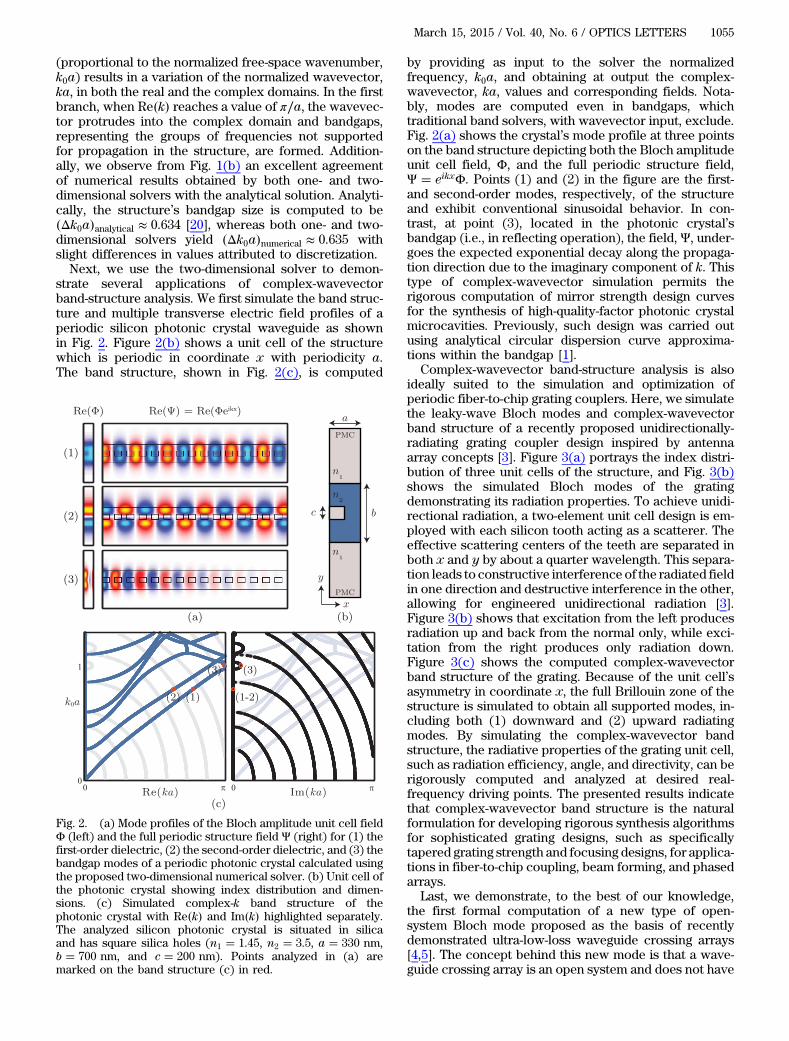
(proportional to the normalized free-space wavenumber,k0a) results in a variation of the normalized wavevector,ka, in both the real and the complex domains. In the firstbranch, when Re�k� reaches a value of π∕a, the wavevec-tor protrudes into the complex domain and bandgaps,representing the groups of frequencies not supportedfor propagation in the structure, are formed. Addition-ally, we observe from Fig. 1(b) an excellent agreementof numerical results obtained by both one- and two-dimensional solvers with the analytical solution. Analyti-cally, the structure’s bandgap size is computed to be�Δk0a�analytical ≈ 0.634 [20], whereas both one- and two-dimensional solvers yield �Δk0a�numerical ≈ 0.635 withslight differences in values attributed to discretization.Next, we use the two-dimensional solver to demon-
strate several applications of complex-wavevectorband-structure analysis. We first simulate the band struc-ture and multiple transverse electric field profiles of aperiodic silicon photonic crystal waveguide as shownin Fig. 2. Figure 2(b) shows a unit cell of the structurewhich is periodic in coordinate x with periodicity a.The band structure, shown in Fig. 2(c), is computed
by providing as input to the solver the normalizedfrequency, k0a, and obtaining at output the complex-wavevector, ka, values and corresponding fields. Nota-bly, modes are computed even in bandgaps, whichtraditional band solvers, with wavevector input, exclude.Fig. 2(a) shows the crystal’s mode profile at three pointson the band structure depicting both the Bloch amplitudeunit cell field, Φ, and the full periodic structure field,Ψ � eikxΦ. Points (1) and (2) in the figure are the first-and second-order modes, respectively, of the structureand exhibit conventional sinusoidal behavior. In con-trast, at point (3), located in the photonic crystal’sbandgap (i.e., in reflecting operation), the field, Ψ, under-goes the expected exponential decay along the propaga-tion direction due to the imaginary component of k. Thistype of complex-wavevector simulation permits therigorous computation of mirror strength design curvesfor the synthesis of high-quality-factor photonic crystalmicrocavities. Previously, such design was carried outusing analytical circular dispersion curve approxima-tions within the bandgap [1].
Complex-wavevector band-structure analysis is alsoideally suited to the simulation and optimization ofperiodic fiber-to-chip grating couplers. Here, we simulatethe leaky-wave Bloch modes and complex-wavevectorband structure of a recently proposed unidirectionally-radiating grating coupler design inspired by antennaarray concepts [3]. Figure 3(a) portrays the index distri-bution of three unit cells of the structure, and Fig. 3(b)shows the simulated Bloch modes of the gratingdemonstrating its radiation properties. To achieve unidi-rectional radiation, a two-element unit cell design is em-ployed with each silicon tooth acting as a scatterer. Theeffective scattering centers of the teeth are separated inboth x and y by about a quarter wavelength. This separa-tion leads to constructive interference of the radiated fieldin one direction and destructive interference in the other,allowing for engineered unidirectional radiation [3].Figure 3(b) shows that excitation from the left producesradiation up and back from the normal only, while exci-tation from the right produces only radiation down.Figure 3(c) shows the computed complex-wavevectorband structure of the grating. Because of the unit cell’sasymmetry in coordinate x, the full Brillouin zone of thestructure is simulated to obtain all supported modes, in-cluding both (1) downward and (2) upward radiatingmodes. By simulating the complex-wavevector bandstructure, the radiative properties of the grating unit cell,such as radiation efficiency, angle, and directivity, can berigorously computed and analyzed at desired real-frequency driving points. The presented results indicatethat complex-wavevector band structure is the naturalformulation for developing rigorous synthesis algorithmsfor sophisticated grating designs, such as specificallytapered grating strength and focusing designs, for applica-tions in fiber-to-chip coupling, beam forming, and phasedarrays.
Last, we demonstrate, to the best of our knowledge,the first formal computation of a new type of open-system Bloch mode proposed as the basis of recentlydemonstrated ultra-low-loss waveguide crossing arrays[4,5]. The concept behind this new mode is that a wave-guide crossing array is an open system and does not have
Fig. 2. (a) Mode profiles of the Bloch amplitude unit cell fieldΦ (left) and the full periodic structure field Ψ (right) for (1) thefirst-order dielectric, (2) the second-order dielectric, and (3) thebandgap modes of a periodic photonic crystal calculated usingthe proposed two-dimensional numerical solver. (b) Unit cell ofthe photonic crystal showing index distribution and dimen-sions. (c) Simulated complex-k band structure of thephotonic crystal with Re�k� and Im�k� highlighted separately.The analyzed silicon photonic crystal is situated in silicaand has square silica holes (n1 � 1.45, n2 � 3.5, a � 330 nm,b � 700 nm, and c � 200 nm). Points analyzed in (a) aremarked on the band structure (c) in red.
March 15, 2015 / Vol. 40, No. 6 / OPTICS LETTERS 1055

a simple light line that separates radiation from guidance.Yet, coupling of two modes via scatterers, through animaginary anti-crossing due to radiative coupling, ena-bles a low-loss Bloch state within the radiation spectrum.Here, we formally compute, for the first time, thislow-loss leaky unidirectional breathing Bloch state.Figure 4 shows the simulated field intensity profile ofthe Bloch-mode crossing design with dimensions chosento achieve the low-radiation state [5]. In this example, thecomputed loss per crossing (i.e., per unit cell) isLdB � −10 log10�e−2 Im�ka�� ≈ 0.06 dB, closely matching re-sults obtained in the initial proposal via FDTD [5]. Thiscomplex-wavevector mode solution establishes that thismode of propagation, after imaginary splitting, is a bonafide leaky eigenstate of the system.As supported by the presented examples and
discussion, we believe that complex-wavevector bandstructure computation has important applications in pho-tonics design. Our finite-difference approach is general,rigorous, scalable, and easily interfaced with FDTDsolvers. Extension of the current two-dimensional TE
implementation to TM fields and three dimensions isstraightforward. We anticipate important applicationsof this method by building synthesis techniques on topof such band structure solvers that will enable rigoroussynthesis of advanced periodic and quasi-periodic pho-tonic devices, including grating couplers, waveguidecrossing arrays, and photonic crystals, as well as phasedarray antennas and other photonic devices.
This work was supported by the National ScienceFoundation award ECCS-1128709.
References
1. Q. Quan and M. Lončar, Opt. Express 19, 18529 (2011).2. D. Taillaert, P. Bienstman, and R. Baets, Opt. Lett. 29, 2749
(2004).3. M. Fan, M. A. Popović, and F. X. Kärtner, Conference on
Lasers and Electro-Optics, OSA Technical Digest (OpticalSociety of America, 2007), paper CTuDD3.
4. Y. Liu, J. M. Shainline, X. Zeng, and M. A. Popović, Opt. Lett.39, 335 (2014).
5. M. A. Popović, E. P. Ippen, and F. X. Kärtner, in Proceedingsof the Annual Meeting of the IEEE Lasers and Electro-Optics Society (IEEE, 2007), p. 56.
6. J. Orcutt, B. Moss, C. Sun, J. Leu, M. Georgas, J. Shainline,E. Zgraggen, H. Li, J. Sun, M. Weaver, S. Urošević, M.Popović, R. Ram, and V. Stojanović, Opt. Express 20,12222 (2012).
7. J. Sun, E. Timurdogan, A. Yaacobi, E. S. Hosseini, and M. R.Watts, Nature 493, 195 (2013).
8. S. Johnson and J. Joannopoulos, Opt. Express 8, 173 (2001).9. A. Archambault, T. V. Teperik, F. Marquier, and J. J. Greffet,
Phys. Rev. B 79, 195414 (2009).10. A. Parzygnat, K. K. Y. Lee, Y. Avniel, and S. G. Johnson,
Phys. Rev. B 81, 155324 (2010).11. K. Huang, E. Lidorikis, X. Jiang, J. Joannopoulos, K. Nelson,
P. Bienstman, and S. Fan, Phys. Rev. B 69, 195111 (2004).12. Y. Ding and R. Magnusson, Opt. Express 15, 680 (2007).13. C. Engström, C. Hafner, and K. Schmidt, J. Comput. Theor.
Nanosci. 6, 775 (2009).14. C. Fietz, Y. Urzhumov, and G. Shvets, Opt. Express 19,
19027 (2011).15. G. Parisi, P. Zilio, and F. Romanato, Opt. Express 20, 16690
(2012).16. W. Chew, J. Appl. Phys. 75, 4843 (1994).17. K. Yee, IEEE Trans. Antennas Propag. 14, 302 (1966).18. K. Radhakrishnan and W. C. Chew, IEEE Trans. Microw.
Theory Tech. 49, 1345 (2001).19. F. Teixeira andW. Chew, IEEE Trans. Antennas Propag. 46,
1386 (1998).20. A. Yariv and P. Yeh, Photonics (Oxford University, 2007).
Fig. 3. (a) Three unit cells of a periodic grating coupler [3]showing index distribution and dimensions. (b) Bloch modeprofiles of the grating at 1550 nm free-space wavelength for(1) downward and (2) upward radiating modes solved usingthe proposed FDFD complex-wavevector solver with PMLboundaries in y and periodicity in x. (c) Simulated complex-wavevector band structure of the grating with Re�k� in blueand Im�k� in black, HSQ and silica light lines shown, and pointsanalyzed in (b) marked in red.
Fig. 4. Low-loss Bloch mode profile intensity, Re�Ψ�2, of a sil-icon waveguide crossing array in silica at 1200 nm wavelengthsimulated with PMLs in y, periodicity in x, a � 2450 nm, andb � 1150 nm displayed (a) to highlight breathing propertyand (b) with scaled ordinate range to show minimal loss.
1056 OPTICS LETTERS / Vol. 40, No. 6 / March 15, 2015