Embed Size (px)
Citation preview
IEEE TRANSACTIONS ON CIRCUITS AND SYSTEMS—I: REGULAR PAPERS, VOL. 60, NO. 2, FEBRUARY 2013 257
Wide Tunning Range 60 GHz VCO and 40 GHz DCOUsing Single Variable Inductor
Tai-You Lu, Chi-Yao Yu, Wei-Zen Chen, Senior Member, IEEE, and Chung-Yu Wu, Fellow, IEEE
Abstract—This paper presents a 60 GHz, 16% tuning rangeVCO, and a 40 GHz, 18 bits, 14% tuning range DCO incorpo-rating variable inductor (VID) techniques. The variable inductor,consisting of a transformer and a variable resistor, is tunable byadjusting its resistor. By employing the proposed frequency tuningscheme, wide-tuning range as well as multi-band operation areachieved without sacrificing their operating frequencies. To verifythe operation principles, the VCO and DCO are both fabricated in90 nm CMOS technology. The tuning range of VCO is from 52.2GHz to 61.3 GHz. The measured phase noise from a 61.3-GHzcarrier is about 118.75 dBc/Hz at 10-MHz offset, and the outputpower is 6.6 dBm. It dissipates 8.7 mW from a 0.7-V supply, andthe chip size is . On the other hand, the DCO iscapable of covering frequency range from 37.6 GHz to 43.4 GHz.The measured phase noise from a 43 GHz carrier is about 109dBc/Hz at 10-MHz offset, and the output power is 11 dBm. TheDCO core dissipates 19 mW from a 1.2-V supply. Chip size is
.
Index Terms—Digital controlled oscillator (DCO), millimeter-wave (MMW) band, ultra wide band (UWB), variable inductor(VID), voltage controlled oscillator (VCO).
I. INTRODUCTION
S HORT RANGE multi-Gbps wireless interconnects havemotivated marvelous research efforts recently [1]–[11]. At
60-GHz unlicensed frequency band, a 7-GHz wide spectrum isavailable for up to 6-Gbps UWB applications. With the rapiddevelopments of the VLSI process, nano-meter CMOS are con-sidered as promising technologies to make RFICs for the broad-band wireless interconnects feasible and cost effective.In the RF transceiver front-end, LC voltage-controlled oscil-
lators (VCOs) are extensively used in frequency synthesizers toprovide local carriers for up and down frequency conversion.Thus its performance is essential to the wireless transceiver.Major design issues of the VCO are focused on oscillating fre-quency, phase noise, output power level, and frequency tuningrange. For portable devices, its power dissipation is also of spe-cial concern.Conventionally, millimeter-wave (MMW) band LC-VCOs
employ accumulation-mode MOS (A-MOS) varactors for
Manuscript received October 17, 2011; revised February 09, 2012; acceptedMarch 06, 2012. Date of publication October 22, 2012; date of current versionJanuary 24, 2013. This work was supported in part by National Nano DeviceLaboratories (NDL), Ansoft Corporation, United Microelectronic Corporation(UMC), and National Science Council (NSC), Taiwan, R.O.C.. This paper wasrecommended by Associate Editor H. Luong.The authors are with the Department of Electronics Engineering and Institute
of Electronics, National Chiao-Tung University, Hsinchu 300, Taiwan (e-mail:[email protected]).Color versions of one or more of the figures in this paper are available online
at http://ieeexplore.ieee.org.Digital Object Identifier 10.1109/TCSI.2012.2215795
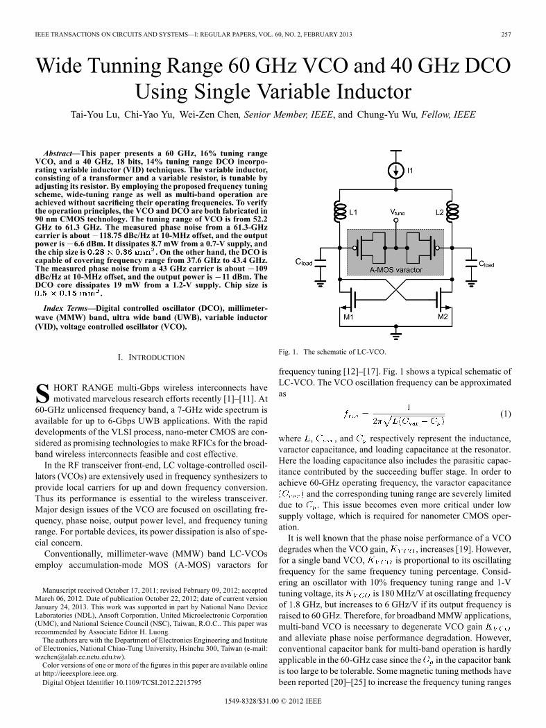
Fig. 1. The schematic of LC-VCO.
frequency tuning [12]–[17]. Fig. 1 shows a typical schematic ofLC-VCO. The VCO oscillation frequency can be approximatedas
(1)
where , , and respectively represent the inductance,varactor capacitance, and loading capacitance at the resonator.Here the loading capacitance also includes the parasitic capac-itance contributed by the succeeding buffer stage. In order toachieve 60-GHz operating frequency, the varactor capacitance
and the corresponding tuning range are severely limiteddue to . This issue becomes even more critical under lowsupply voltage, which is required for nanometer CMOS oper-ation.It is well known that the phase noise performance of a VCO
degrades when the VCO gain, , increases [19]. However,for a single band VCO, is proportional to its oscillatingfrequency for the same frequency tuning percentage. Consid-ering an oscillator with 10% frequency tuning range and 1-Vtuning voltage, its is 180MHz/V at oscillating frequencyof 1.8 GHz, but increases to 6 GHz/V if its output frequency israised to 60 GHz. Therefore, for broadbandMMW applications,multi-band VCO is necessary to degenerate VCO gainand alleviate phase noise performance degradation. However,conventional capacitor bank for multi-band operation is hardlyapplicable in the 60-GHz case since the in the capacitor bankis too large to be tolerable. Some magnetic tuning methods havebeen reported [20]–[25] to increase the frequency tuning ranges
1549-8328/$31.00 © 2012 IEEE
258 IEEE TRANSACTIONS ON CIRCUITS AND SYSTEMS—I: REGULAR PAPERS, VOL. 60, NO. 2, FEBRUARY 2013
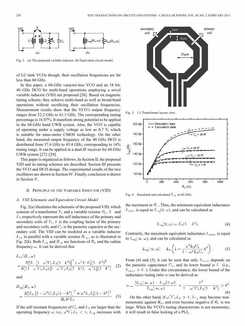
Fig. 2. (a) The proposed variable inductor. (b) Equivalent circuit model.
of LC-tank VCOs though, their oscillation frequencies are farless than 60 GHz.In this paper, a 60-GHz varactor-less VCO and an 18 bit,
40 GHz DCO for multi-band operations employing a novelvariable inductor (VID) are proposed [26]. Based on magnetictuning scheme, they achieve multi-band as well as broad-bandoperations without sacrificing their oscillation frequencies.Measurement results show that the VCO’s output frequencyranges from 52.2 GHz to 61.3 GHz. The corresponding tuningpercentage is 16.07%. It manifests strong potential to be appliedin the 60-GHz band UWB system. Also, the VCO is capableof operating under a supply voltage as low as 0.7 V, whichis suitable for nano-meter CMOS technology. On the otherhand, the measured output frequency of the 40 GHz DCO isdistributed from 37.6 GHz to 43.4 GHz, corresponding to 14%tuning range. It can be applied in a dual-IF receiver for 60 GHzUWB system [27]–[29].This paper is organized as follows. In Section II, the proposed
VID and its tuning schemes are described. Section III presentsthe VCO and DCO design. The experimental results of the twooscillators are shown in Section IV. Finally, conclusion is drawnin Section V.
II. PRINCIPLE OF THE VARIABLE INDUCTOR (VID)
A. VID Schematic and Equivalent Circuit Model
Fig. 2(a) illustrates the schematic of the proposed VID, whichconsists of a transformer and a variable resistor . andrespectively represent the self inductance of the primary and
secondary coils of , is the coupling factor of the primaryand secondary coils, and is the parasitic capacitor at the sec-ondary coil. The VID can be modeled as a variable inductor
in parallel with a variable resistor , as is illustrated inFig. 2(b). Both and are functions of and the radianfrequency . It can be derived that
(2)
and
(3)
If the self resonant frequencies of and are larger than theoperating frequency , i.e., , increases with
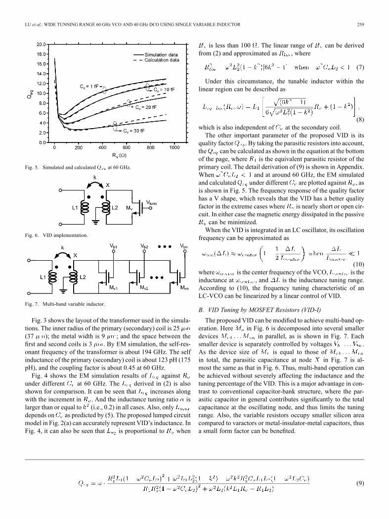
Fig. 3. 1:1 Transformer layout view.
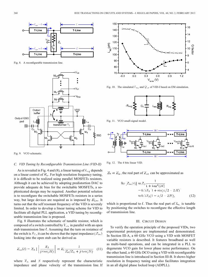
Fig. 4. Simulated and calculated at 60 GHz.
the increment in . Thus, the minimum equivalent inductanceis equal to , and can be calculated as
(4)
Contrarily, the maximum equivalent inductance is equalto , and can be calculated as
(5)
From (4) and (5), it can be seen that only depends onthe parasitic capacitance , and its lower bound is (i.e.,
). Under this circumstance, the lower bound of theinductance tuning ratio can be derived as
(6)On the other hand, if , may become non-
monotonic against , and even become negative if is toolarge. When the VCO’s tuning characteristic is not monotonic,it will result in false locking of a PLL.
LU et al.: WIDE TUNNING RANGE 60 GHz VCO AND 40 GHz DCO USING SINGLE VARIABLE INDUCTOR 259
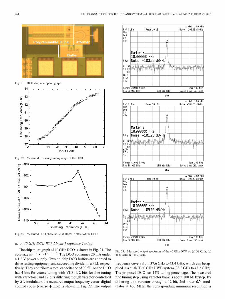
Fig. 5. Simulated and calculated at 60 GHz.
Fig. 6. VID implementation.
Fig. 7. Multi-band variable inductor.
Fig. 3 shows the layout of the transformer used in the simula-tions. The inner radius of the primary (secondary) coil is 25(37 ); the metal width is 9 ; and the space between thefirst and second coils is 3 . By EM simulation, the self-res-onant frequency of the transformer is about 194 GHz. The selfinductance of the primary (secondary) coil is about 123 pH (175pH), and the coupling factor is about 0.45 at 60 GHz.Fig. 4 shows the EM simulation results of against
under different at 60 GHz. The derived in (2) is alsoshown for comparison. It can be seen that increases alongwith the increment in . And the inductance tuning ratio islarger than or equal to (i.e., 0.2) in all cases. Also, onlydepends on as predicted by (5). The proposed lumped circuitmodel in Fig. 2(a) can accurately represent VID’s inductance. InFig. 4, it can also be seen that is proportional to when
is less than 100 . The linear range of can be derivedfrom (2) and approximated as , where
(7)
Under this circumstance, the tunable inductor within thelinear region can be described as
(8)which is also independent of at the secondary coil.The other important parameter of the proposed VID is its
quality factor . By taking the parasitic resistors into account,the can be calculated as shown in the equation at the bottomof the page, where is the equivalent parasitic resistor of theprimary coil. The detail derivation of (9) is shown in Appendix.When and at around 60 GHz, the EM simulatedand calculated under different are plotted against , asis shown in Fig. 5. The frequency response of the quality factorhas a V shape, which reveals that the VID has a better qualityfactor in the extreme cases where is nearly short or open cir-cuit. In either case the magnetic energy dissipated in the passivecan be minimized.When the VID is integrated in an LC oscillator, its oscillation
frequency can be approximated as
(10)where is the center frequency of the VCO, is theinductance at , and is the inductance tuning range.According to (10), the frequency tuning characteristic of anLC-VCO can be linearized by a linear control of VID.
B. VID Tuning by MOSFET Resistors (VID-I)
The proposed VID can be modified to achieve multi-band op-eration. Here in Fig. 6 is decomposed into several smallerdevices in parallel, as is shown in Fig. 7. Eachsmaller device is separately controlled by voltages .As the device size of is equal to those ofin total, the parasitic capacitance at node in Fig. 7 is al-most the same as that in Fig. 6. Thus, multi-band operation canbe achieved without severely affecting the inductance and thetuning percentage of the VID. This is a major advantage in con-trast to conventional capacitor-bank structure, where the par-asitic capacitor in general contributes significantly to the totalcapacitance at the oscillating node, and thus limits the tuningrange. Also, the variable resistors occupy smaller silicon areacompared to varactors or metal-insulator-metal capacitors, thusa small form factor can be benefited.
(9)
260 IEEE TRANSACTIONS ON CIRCUITS AND SYSTEMS—I: REGULAR PAPERS, VOL. 60, NO. 2, FEBRUARY 2013
Fig. 8. A reconfigurable transmission line.
Fig. 9. VCO schematic.
C. VID Tuning by Reconfigurable Transmission Line (VID-II)
As is revealed in Fig. 4 and (8), a linear tuning of dependson a linear control of . For high resolution frequency tuning,it is difficult to be realized using parallel MOSFETs resistors.Although it can be achieved by adopting predistortion DAC toprovide adequate dc bias for the switchable MOSFETs, a so-phisticated design may be required. Another potential solutionis to reconfigure the switchable MOSFETs resistors in a seriesway, but large devices are required as is imposed by . Itturns out that the self resonant frequency of the VID is severalylimited. In order to develop a linear tuning scheme for VID tofacilitate all digital PLL application, a VID tuning by reconfig-urable transmission line is proposed.Fig. 8 illustrates the schematic of tunable resistor, which is
composed of a switch controlled by in parallel with an openstub transmission line . Assuming that the turn on resiatnce ofthe switch is , it can be shown that the input impedancelooking into the open stub can be derived as
(11)
where and respectively represent the characteristicimpedance and phase velocity of the transmission line. If
Fig. 10. The simulated and of VID-I based on EM simulation.
Fig. 11. VCO small-signal model.
Fig. 12. The 4 bits linear VID.
, the real part of can be approximated as
(12)
which is proportional to . Thus the real part of is tunableby positioning the switches to reconfigure the effective lengthof transmission line.
III. CIRCUIT DESIGN
To verify the operation principle of the proposed VIDs, twoexperimental prototypes are implemented and demonstrated.In Section III-A, a 60 GHz VCO using a VID with MOSFETvariable resistors is described. It features broadband as wellas multi-band operations, and can be integrated in a PLL todegenerate VCO gain for lower phase noise performance. Onthe other hand, a 40 GHz DCO using a VID with reconfigurabletransmission line is introduced in Section III-B. It shows higherresolution in frequency tuning and also facilitates integrationin an all digital phase locked loop (ADPLL).

LU et al.: WIDE TUNNING RANGE 60 GHz VCO AND 40 GHz DCO USING SINGLE VARIABLE INDUCTOR 261
Fig. 13. (a) The EM simulated and calculated . (b) Equivalent induc-tance and quality factor of 4-bits VID-II based on EM simulation.
A. 60 GHz Multi-Band VCO
The detail schematic for 60 GHz, multi-band VCO is showin Fig. 9. In order to reduce the parasitic capacitance at the res-onator, the negative impedance converter is composed ofand cross-coupled pair. is an output buffer to drive the50- load for measurement, and is a dummy buffer to bal-ance the parasitic capacitance at the resonator.The variable resistors consists of six binary-weighted
NMOSFETs controlled by digital codes ( – )for band switching, and an NMOS controlled byfor fine frequency tuning. Thus and are tunable byadjusting or . The second coil is centertapped to ground, so as to diminish dc power dissipation.For a better quality factor, the self resonant frequency at thesecondary port caused by and the parasitic capacitance ofMOSFETs should be designed to be higher than the operatingfrequency of the VID.In the experimental prototype, a single-turn 1:1 transformer
is adopted in the VID, as is shown in Fig. 3. To illustrate andacross different band of operations, and
are wired together and controlled by . The simulatedand of VID (VID-I) at 60-GHz are illustrated in Fig. 10.When changes from 0.3 to 1.2 V, the is tunable
Fig. 14. The schematic of DCO.
Fig. 15. VCO chip micrograph.
from 142 to 103 pH (i.e., ), and the quality factor ischanged from 11.35 to 3.6. The VID has a better quality factorwhen MOSFET resistors are nearly fully turned on or off, i.e.,is minimum or maximum. This agrees pretty well with the
calculated results shown in (9) and Fig. 5.The equivalent small-signal model of the VCO is shown in
Fig. 11. Here represents the total capacitance at the res-onator, including the parasitic capacitances of the cross-cou-pled pair , the output buffer , and the parasiticcapacitance of the transformer . is the equivalent resis-tance looking into the primary coil of the VID, as is derivedin (3). The negative resistance provided by the cross-coupledpair M1 and M2 is denoted as , which is approximatelyequal to , and is the small-signal transconductance

262 IEEE TRANSACTIONS ON CIRCUITS AND SYSTEMS—I: REGULAR PAPERS, VOL. 60, NO. 2, FEBRUARY 2013
Fig. 16. Measured/simulated frequency tuning characteristic and output powerof 60 GHz VCO.
of . must be smaller than to guarantee oscil-lation start-up. In this design, is chosen to be smaller than
within the entire frequency range. The oscillating fre-quency of the VCO can be derived as
(13)
, and the upper and lower bound of output fre-quencies are
(14)
and
(15)
Based on (14) and (15), the VCO frequency tuning percentagecan be derived and is approximated by , which is deter-mined by the coupling factor of the transformer. Therefore,for a VCO with a given transformer to implement the VID, itsfrequency tuning range can be quickly estimated. In this design,the coupling factor of the transformer is around 0.45, it turns outthat the frequency tuning range of the VCO is at least 10%.
B. A 40 GHz DCO With Linear Frequency Tuning
To further linearize the frequency tuning characteristic ofVID, a 40 GHz DCO with reconfigurable transmission line isimplemented. Fig. 12 shows the detail schematic of a 4-bitslinearly controlled VID (VID-II) for coarse tuning. The trans-mission line is divided equally into 16 segments with 16 MOSswitches attched on it. Thus the effective length of the open stubis programable by the switches, and the parasitic capacitanceassociated with the MOS switches can be absorbed along thetransmission line. Based on (7) and (8), the frequency tuning
Fig. 17. Measured VCO tuning characteristics under different supply voltages.
Fig. 18. Measured frequency tuning characteristics of all bands of the 60 GHzVCO.
range of the DCO with linear frequency tuning can bederived as
(16)
The physical length of the transmission line is 15 . ByEM simulation, , and of the transformer are 100 pH,129 pH and 0.6, while and are 46 and 0.08respectively. It turns out that the corresponing frequency tuningrange is at least 13% according to (16).Fig. 13(a) shows the EM simulated and that derived by
(12). Both illustrate linear characteristic along the tuning range.Fig. 13(b) shows the equivalent inductance and quality factorof the linearly controlled VID by EM simulation. The corre-sponding inductance is distributed from 58 pH to 82 pH, whileQ is varied between 5.5 to 3.8 due to the change of real part of.Fig. 14 shows the detail schematic of the 40 GHz digitally
controlled oscillator (DCO). The DCO has 4 bits for coarsetuning with VID-II, 2 bits for fine tuning with varactors, and12 bits dithering though varactor controlled by a 2nd order

LU et al.: WIDE TUNNING RANGE 60 GHz VCO AND 40 GHz DCO USING SINGLE VARIABLE INDUCTOR 263
Fig. 19. Measured phase noise at 10-MHz offset in single-band and multi-bandoperation of the 60 GHz VCO.
modulator at 400MHz. The correspondingminimum gain of theDCO is about 24 kHz/step.
IV. MEASUREMENT RESULTS
A. 60 GHz Single and Multi-Band VCO
Fig. 15 shows the chip micrograph of the 60 GHz VCO.The core size is . The chip is measured ona high-frequency probe station. With , the mea-sured and simulated frequency tuning characteristics are shownin Fig. 16. If the tuning voltages of and in Fig. 9are tied together and varied from 0.3 to 1.2 V, the single bandVCO frequency is changed from 52.2 to 61.32 GHz. The cor-responding tuning percentage is 16.07%. With a reduced tuningrange of 0 V to 0.7 V, the tuning percentage becomes 13.98%.After the loss from the output buffer, probes, cables, adapters,and external mixer is deembedded, the measured single-endedoutput power are also shown in Fig. 16. Here the simulation re-sults are also shown for comparison. From the measurement re-sults, the VCO output power varies from 10 dBm to 4 dBmwithin the entire frequency tuning range.The VCO can start oscillation as VDD is larger than 0.37 V.
The measured frequency tuning ranges for VDD from 0.4 V to0.9 V are shown in Fig. 17. When , the VCO hasthe maximum frequency tuning range from 54.07 to 64 GHz(i.e., 16.8% at 59 GHz). Under this circumstance, the parasiticcapacitance introduced by negative impedance converter is min-imized.Multi-band operation is achieved by digitally controlling– and fine-tuning separately. By the mixed-mode
frequency tuning scheme, the VCO manifests 64 frequencybands incorporating binary weighted transistors – , asis shown in Fig. 18. The maximum is 720 MHz/V atband 8, which is reduced by 10 fold compared to that of asingle-band operation. The uniformity of multi-band operationscan be improved by more sophisticated transistor sizing insteadof employing binary-weighted transistors.
Fig. 20. Measured output spectrums of the 60 GHz VCO at (a) 52.19 GHz (b)54.55 GHz (c) 61.3 GHz.
The measured phase noise performance at 10-MHz offsetwithin the entire frequency tuning range is plotted in Fig. 19.By multi-band operation, the phase noise performance rangesfrom 94 to 118.75 dBc/Hz, and the average phase noise is102.44 dBc/Hz. If – and are tied together for a
single-band frequency tuning, the measured phase noise is alsoshown for comparison. It can be observed that phase noise per-formance can be significantly improved by 10 to 30 dB em-ploying the proposed multi-band operation scheme.Fig. 20(a)–(c) show the measured VCO output spectrums
at different frequencies. When , the measuredaverage power consumptions of the VCO core within thefrequency tuning range is 8.7 mW. The buffer stage dissipates5.6 mW.
264 IEEE TRANSACTIONS ON CIRCUITS AND SYSTEMS—I: REGULAR PAPERS, VOL. 60, NO. 2, FEBRUARY 2013
Fig. 21. DCO chip microphotograph.
Fig. 22. Measured frequency tuning range of the DCO.
Fig. 23. Measured DCO phase noise at 10-MHz offset of the DCO.
B. A 40 GHz DCO With Linear Frequency Tuning
The chipmicrograph of 40GHzDCO is shown in Fig. 21. Thecore size is . The DCO consumes 20 mA undera 1.2 V power supply. Two on-chip DCO buffers are adopted todrive testing equipment and succeeding divider in a PLL respec-tively. They contribute a total capacitance of 90 fF. As the DCOhas 4 bits for coarse tuning with VID-II, 2 bits for fine tuningwith varactors, and 12 bits dithering though varactor controlledby modulator, the measured output frequency versus digitalcontrol codes (coarse fine) is shown in Fig. 22. The output
Fig. 24. Measured output spectrums of the 40 GHz DCO at: (a) 38 GHz; (b)41.6 GHz; (c) 43.3 GHz.
frequency covers from 37.6 GHz to 43.4 GHz, which can be ap-plied in a dual-IF 60GHzUWB system (38.8 GHz to 43.2 GHz).The proposed DCO has 14% tuning percentage. The measuredfine tuning step using varactor bank is about 100 MHz/step. Bydithering unit varactor through a 12 bit, 2nd order mod-ulator at 400 MHz, the corresponding minimum resolution is

LU et al.: WIDE TUNNING RANGE 60 GHz VCO AND 40 GHz DCO USING SINGLE VARIABLE INDUCTOR 265
TABLE IPERFORMANCE BENCHMARK
about 24 kHz/step by simulation. Taking signal loss caused byexperimental setup into account (including the loss of probes,cables and adapters), the output power varies from 15 dBmto 11 dBm due to the variation of quality factor within theentire frequency tuning range. The measured phase noise per-formance at 10-MHz offset within the entire frequency tuningrange is plotted in Fig. 23. Fig. 24 shows the measured VCOoutput spectrums at different frequencies.The performance benchmark of the proposed oscillators and
the prior art in the literature are summarized in Table I. Threedifferent figures of merits are illustrated to investigate their ad-vantages. They are
(17)
(18)
(19)
where is the phase noise at the offset frequency , isthe oscillating frequency, is the power consumption,is the frequency tuning percentage, and is tuning voltagerange. For over 50-GHz operating frequency, the proposedVCOhas the widest frequency tuning range, the best and
. On the other hand, the proposed DCO has the widesttuning range for over 40 GHz operation frequency, while alsomanifests the finest frequency resolution of 24 kHz. Comparedto the FoM of VCO, it suggests that the Q-factor of DCO tankis compromised with resolution and tuning range.
Fig. 25. The modified lump model of the VID.
V. CONCLUSION
Novel variable inductors for VCO and DCO are proposedin this paper. By using the proposed frequency tuning scheme,both VCO and DCO are capable of operating at MMW fre-quency band while manifesting wider tuning range than thoseVCOs with varactors for frequency tuning. In addition, multi-band operation can be achieved without sacrificing its oscil-lating frequency or consuming large chip area. Both the VCOandDCO are capable of operating at supply voltage as low as 0.7V. They manifest strong potential to be applied in the 60-GHzUWB system.
APPENDIX
Fig. 25 shows the modified lumped model of the VID to an-alyze its equivalent quality factor . and respectivelyrepresent the parasitic resistors at the primary and secondarycoils. The input impedance can be calculated as
(20)
266 IEEE TRANSACTIONS ON CIRCUITS AND SYSTEMS—I: REGULAR PAPERS, VOL. 60, NO. 2, FEBRUARY 2013
(23)
where
(21)
In general, is much smaller than . Thus, when, can be simplified as
(22)
The equivalent quality factor of the VID can be calculatedas shown in the equation at the top of the page.
REFERENCES
[1] C. H. Doan, S. Emami, A. M. Niknejad, and R. W. Brodersen, “Mil-limeter-wave CMOS design,” IEEE J. Solid-State Circuit, vol. 40, no.1, pp. 144–155, Jan. 2005.
[2] B. Razavi, “A 60-GHz CMOS receiver front-end,” IEEE J. Solid-StateCircuit, vol. 41, no. 1, pp. 17–22, Jan. 2006.
[3] B. Razavi, “CMOS transceivers for the 60-GHz band,” in IEEE RadioFreq. Integr. Circuit Symp. Dig., San Francisco, CA, Jun. 2006, pp.11–13.
[4] T. Yao,M. Gordon, K. Yau,M. T. Yang, and S. P. Voinigescu, “60-GHzPA and LNA in 90-nmRF-CMOS,” in IEEERadio Freq. Integr. CircuitSymp. Dig., San Francisco, CA, Jun. 2006, pp. 147–150.
[5] S. Emami, C. H. Doan, A. M. Niknejad, and R. W. Bronderson, “A60-GHz down-converting CMOS single-gate mixer,” in IEEE RadioFreq. Integr. Circuit Symp. Dig., Long Beach, CA, Jun. 2005, pp.163–166.
[6] A. Hajimire, “mm-wave silicon ICs: Challenges and opportunities,”in IEEE Custom Integr. Circuits Conf. (CICC) Dig., Sep. 2007, pp.741–747.
[7] B. Razavi, “A millimeter-wave CMOS heterodyne receiver withon-chip LO and divider,” IEEE J. Solid-State Circuit, vol. 43, no. 2,pp. 477–485, Feb. 2008.
[8] C. S. Wang, J. W. Huang, S. H. Wen, S. H. Yeh, and C. K. Wang,“A CMOS RF front-end with on-chip antenna for V-band broadbandwireless communications,” inProc. Eur. Solid-State Circuit Conf., Sep.2007, pp. 143–146.
[9] S. Emami, C. H. Doan, A. M. Niknejad, and R. W. Brodersen, “Ahighly integrated 60 GHz CMOS front-end receiver,” in IEEE Int.Solid-State Circuit Conf. Dig., Feb. 2007, pp. 190–191.
[10] A. Parsa and B. Razavi, “A 60 GHz CMOS receiver using a 30 GHzLO,” in IEEE Int. Solid-State Circuit Conf. Dig., Feb. 2008, pp.190–191.
[11] T. Mitomo, R. Fujimoto, N. Ono, R. Tachibana, H. Hoshino, Y. Yoshi-hara, Y. Tsutsumi, and I. Seto, “A 60-GHz CMOS receiver with fre-quency synthesizer,” IEEE J. Solid-State Circuits, vol. 43, no. 4, pp.1030–1037, Apr. 2008.
[12] H. Wang, “A 50 GHz VCO in 0.25 CMOS,” in IEEE Int. Solid-Satate Circuits Conf. Dig. Tech. Papers, Feb. 2001, pp. 372–373.
[13] M. Teibout, “A 51 GHz VCO in 0.13 CMOS,” in IEEE Int. Solid-Satate Circuits Conf. Dig. Tech. Papers, Feb. 2002, pp. 300–301.
[14] C. Cao and K. K. O, “Millimeter-wave voltage-controlled oscillatorsin 0.13- technology,” IEEE J. Solid-State Circuits, vol. 41, no. 6,pp. 1297–1304, Jun. 2006.
[15] D. Huang, W. Hant, N.-Y. Wang, T. W. Ku, Q. Gu, R. Wong, andM.-C. F. Chang, “A 60 GHz CMOS VCO using on-chip resonatorwith embedded artificial dielectric for size, loss and noise reduction,”in IEEE Int. Solid-Satate Circuits Conf. Dig. Tech. Papers, Feb. 2006,pp. 314–315.
[16] K. Ishibashi, M.Motoyoshi, N. Kobayashi, andM. Fujishima, “76 GHzCMOS voltage-controlled oscillator with 7% frequency tuning range,”in Symp. VLSI Circuit Dig. Tech. Papers, Jun. 2007, pp. 176–177.
[17] J. Borremans, M. Dehan, K. Scheir, M. Kuijk, and P. Wambacq, “VCOdesign for 60 GHz applications using differential shielded inductorsin 0.13 CMOS,” in IEEE Radio Freq. Integr. Circuit Symp. Dig.,Atlanta, GA, Jun. 2008, pp. 135–138.
[18] H. K. Chen, H. J. Chen, D. C. Chang, Y. Z. Juang, and S. S. Lu, “A0.6 V, 4.32 mW, 68 GHz low phase noise VCO with intrinsic-tunedtechnique in 0.13 CMOS,” IEEE Microw. Wireless Compon. Lett.,vol. 18, no. 7, pp. 467–469, Jul. 2008.
[19] N. H. W. Fong, J. O. Plouchart, N. Zamdmer, D. Liu, L. F. Wagner, C.Plett, and N. G. Tarr, “Design of wind-band CMOSVCO for multibandWirless LAN application,” IEEE J. Solid-State Circuit, vol. 38, no. 8,pp. 1333–1342, Aug. 2003.
[20] M. Demirkan, S. P. Bruss, and R. R. Spencer, “Design of wide tuning-range CMOSVCOs using switched coupled-inductors,” IEEE J. Solid-State Circuits, vol. 43, no. 5, pp. 1156–1163, May 2008.
[21] L. Geynet, E. D. Foucauld, P. Vincent, and G. Jacquemod, “Fully-in-tegrated multi-standard VCOs with switched LC tank and power con-trolled by body voltage in 130 nm CMOS/SOI,” in Proc. IEEE RadioFreq. Integr. Circuit Symp., 2006.
[22] S. Rong and H. C. Luong, “Analysis and design of transformer-baseddual-band VCO for software-defined radios,” IEEE Trans. CircuitsSyst. I, Reg. Papers, vol. 59, no. 3, pp. 449–462, Mar. 2012.
[23] G. Liu, R. Berenguer, and Y. Xu, “A MM-wave configurableVCO using MCPW-based tunable inductor in 65-nm CMOS,”IEEE Trans. Circuits Syst. II, Exp. Briefs, vol. 58, no. 12,pp. 842–846, Dec. 2011.
[24] J. Yang, C.-Y. Kim, D.-W. Kim, and S. Hong, “Design of a 24-GHzCMOSVCOwith an asymmetric-width transformer,” IEEE Trans. Cir-cuits Syst. II, Exp. Briefs, vol. 57, no. 3, pp. 173–177, Mar. 2010.
[25] A. Tanabe, K. Hijioka, H. Nagase, and Y. Hayashi, “A novel variableinductor using a bridge circuit and its application to a 5–20GHz tunableLC-VCO,” IEEE J. Solid-State Circuits, vol. 46, no. 4, pp. 883–893,Apr. 2011.
[26] C.-Y. Yu, W.-Z. Chen, C.-Y. Wu, and T.-Y. Lu, “A 60-GHz, 14%tuning range, multi-band VCOwith a single variable inductor,” in IEEEAsian Solid-State Circuits Conf. Dig. Tech. Papers, Nov. 2008, pp.129–132.
[27] I. Bashir, R. B. Staszewski, O. Eliezer, B. Banerjee, and P. T. Balsara,“A novel approach for mitigation of RF oscillator pulling in a polartransmitter,” IEEE J. Solid-State Circuits, vol. 46, no. 2, pp. 403–415,Feb. 2011.
[28] J. Zhang, K. Waheed, and R. B. Staszewski, “A technique to reducephase/frequency modulation bandwidth in a polar RF transmitter,”IEEE Trans. Circuit Syst. I, Reg. Papers, vol. 57, no. 8, pp. 2010–2207,Aug. 2010.
[29] R. B. Staszewski, R. Staszewski, J. L. Wallberg, T. Jung, C.-M.Hung, J. Koh, D. Leipold, K. Maggio, and P. T. Balsara,“SoC with an integrated DSP and a 2.4-GHz RF transmitter,”IEEE Trans. Very Large Scale Integr. (VLSI) Syst., vol. 13,no. 11, pp. 1253–1265, Nov. 2005.
[30] T. LaRocca, J. Liu, F. Wang, D. Murphy, and F. Chang, “CMOS digitalcontrolled oscillator with embedded DiCAD resonator for 58–64 GHzlinear frequency tuning and low phase noise,” in Proc. IEEE Int. Micro.Symp., Jul. 2009, pp. 685–688.
[31] R. Genesi, F. M. De Paola, and D. Manstretta, “A 53 GHz DCO formm-wave WPAN,” in Proc. IEEE Custom Integr. Circuits Conf., Sep.2008, pp. 571–574.
LU et al.: WIDE TUNNING RANGE 60 GHz VCO AND 40 GHz DCO USING SINGLE VARIABLE INDUCTOR 267
Tai-You Lu was born in Taipei, Taiwan, in 1980. Hereceived the B.S. degrees in electrical engineeringfrom National Cheng-Kung University, Tainan,Taiwan, in 2003, and the Ph.D. degree in electronicsengineering from National Chiao Tung University,Hsinchu, Taiwan, in 2011.He has been with MediaTek Inc., Taiwan, since
2011, where he is working on analog IC design. Hiscurrent research focused on mixed-signal integratedcircuit for wireless and wireline communication sys-tems.
Dr. Lu is a member of Phi-Tau-Phi honorary scholar society.
Chi-Yao Yu (M’10) was born in Taipei, Taiwan, in1978. He received the M.S. degree in communica-tion engineering from National Tsing Hua Univer-sity, Hsinchu, Taiwan, in 2002, and the Ph.D. degreein electronics engineering from National Chiao TungUniversity, Hsinchu, in 2008.He has been with MediaTek Inc., Taiwan, since
2008, where he is working on analog and RF ICdesign for wireless communications. His currentresearch interest is ultra-high dynamic range receiverfor cellular system.
Wei-Zen Chen received the B.S., M.S., and Ph.D.degree in electronics engineering from NationalChiao-Tung University, Hsin-Chu, Taiwan, in 1992,1994, and 1999, respectively.He was with ITRI/ERSO in 1999 involved in the
development of CMOS RF ICs for cellular and wire-less LAN applications. From 1999 to 2002, he wasan assistant Professor at the Department of ElectricalEngineering, National Central University, Chung-Li,Taiwan. Since 2002, he joined the Department ofElectronics Engineering, National Chiao-Tung Uni-
versity, where he is now a full Professor. His research focuses on mixed-signalintegrated circuit for wireless and wireline communication systems, withspecial emphasis on Serdes, high speed interface, optical communication,wireless PAN, LAN, and body area network applications.
Dr. Chen was the deputy executive director of National SoC (NSoC) Programin Taiwan from 2009–2011, and is the principal investigator of National Projecton Intelligent Electronics (NPIE) in Taiwan since 2011. He also serves as IEEESolid-State Circuit Society Taipei Chapter chairman starting from 2008. He wasthe technical program vice chair of 2008 VLSI/CAD design symposium, tech-nical program chair of 2012 symposium on engineering, medical, and biologyapplications (SEMBA), and the guest editor of International Journal of Elec-trical Engineering (IJEE). He is a member of Phi-Tau-Phi honorary scholar so-ciety, and also served as technical program committee member of IEEE CustomIntegrated Circuits Conference (CICC), IEEE Asian Solid-State Circuit Confer-ence (A-SSCC), IEEE RFIT, and IEEE ASICON.
Chung-Yu Wu (S’76–M’76–SM’96–F’98) wasborn in 1950. He received the M.S. and Ph.D.degrees from the Department of Electronics Engi-neering, National Chiao Tung University, Hsinchu,Taiwan, in 1976 and 1980, respectively. In addition,he conducted visiting research at UC Berkeley inSummer 2002.Since 1980, he has served as a consultant to high-
tech industry and research organizations and has builtup strong research collaborations with high-tech in-dustries. From 1980 to 1983, he was an Associate
Professor at National Chiao Tung University. During 1984 to 1986, he was aVisiting Associate Professor in the Department of Electrical Engineering, Port-land State University, Portland, OR. Since 1987, he has been a Professor at Na-tional Chiao Tung University. From 1991 to 1995, he was rotated to serve as theDirector of the Division of Engineering and Applied Science on the NationalScience Council, Taiwan. From 1996 to 1998, he was honored as the Centen-nial Honorary Chair Professor at National Chiao Tung University. Currently,he is the Chair Professor at National Chiao Tung University. He has publishedmore than 300 technical papers in international transactions/journals and con-ferences. He also has 38 patents including 19 U.S. patents. His research inter-ests are biomedical electronics, nanoelectronics and VLSI including circuits andsystems in low-power/low-voltage mixed-signal design, neural vision sensors,neuromorphic network, and RF circuits.Dr. Wu is a member of Eta Kappa Nu and Phi Tau Phi Honorary Scholastic
Societies. He was a recipient of IEEE Fellow Award in 1998 and Third Millen-nium Medal in 2000. In Taiwan, he received numerous research awards fromMinistry of Education, National Science Council, and professional foundations.