Embed Size (px)
Citation preview

270 IEEE TRANSACTIONS ON CIRCUITS AND SYSTEMS—I: REGULAR PAPERS, VOL. 57, NO. 1, JANUARY 2010
Multi-Gb/s Bit-by-Bit Receiver Architectures for 1-DPartial-Response Channels
Masum Hossain and Anthony Chan Carusone, Senior Member, IEEE
Abstract—Low-complexity bit-by-bit detection techniques for1-D partial-response channels are presented. First, a full-ratedetection technique is presented which operates at 3.3 Gb/s con-suming 40 mA from a 1.8-V supply with a sensitivity of 40-mVdifferential. The speed of the full-rate architecture is limited bythe settling time of a latch circuit which has to be less than 1UI. To eliminate this limitation, a novel demuxing technique isintroduced. Using the proposed technique, a second architectureachieves 5 Gb/s data rate with the same sensitivity and consuming62 mA (including output buffer) from 1.8-V supply. Both half-rateand full-rate architectures are also studied in 90-nm CMOStargeting chip-to-chip applications. The implemented full-ratearchitecture operates at 10 Gb/s consuming 32 mW, whereas thesimulated half-rate architecture consumes 50 mW and operates at16.67 Gb/s.
Index Terms—AC coupling, clockless demuxing, decision feed-back equalization (DFE), dicode channel, half-rate, peak detection.
I. INTRODUCTION
T HERE ARE many new and emerging applications for di-code (1-D) partial-response signaling. Dicode partial-re-
sponse signaling was applied to magnetic storage channels [1].More recently, a similar channel response has been observed inmulti-Gb/s wireline communication applications such as pas-sive optical networks (PON) and ac-coupled chip-to-chip linksthat have spectral nulls at dc. The speed of the receivers for theseapplications is generally limited by the settling time of a latchcircuit. This shortcoming is addressed in this paper with twonovelties: First, an improved latch circuit provides faster settlingtime, and second, a parallel architecture permits the positive-and negative-going pulses to be detected separately, thus allevi-ating the feedback settling-time requirements on the latches.
One interesting area where partial-response signaling hasbeen applied is chip-to-chip links. For example, it was used fora high-speed multidrop bus with magnetically coupled receivers[2]. Capacitive coupling has also been used in chip-to-chiplinks within a package [3] and over printed circuit board tracesof up to 20 cm in length [4]. AC coupling has also been usedfor bidirectional signaling [5], as a wireless link for modulateddata [6] and for power transfer [7].
Manuscript received September 19, 2008; revised January 27, 2009. Firstpublished March 27, 2009; current version published February 02, 2010. Thiswork was supported in part by Intel Corporation and in part by Broadcom. Thispaper was recommended by Associate Editor A. Demosthenous.
The authors are with the Department of Electrical and Computer Engineering,University of Toronto, Toronto, ON M5T 1X2, Canada (e-mail: [email protected]; [email protected]).
Digital Object Identifier 10.1109/TCSI.2009.2019391
Fig. 1. Recent applications of 1-D partial-response channels.
Another area of interest is burst-mode applications. In a PONsystem, the receiver at the optical line terminal (OLT) needs torecover data from different optical-network units (ONUs). Thepackets of data from ONUs arrive in bursts at the OLT end, andtheir signal strength varies significantly. For high data rates suchas 10 Gb/s, the receiver used in the OLT end needs to recoverthe dc information in less than 1 ns. To avoid the difficulty as-sociated with fast dc extraction, 1-D channel is used to suppressthe dc content [8].
Partial-response channel receivers can be broadly classifiedinto two categories: sequence detectors and bit-by-bit detectors.Sequence detectors, such as those using the Viterbi algorithm,make a decision based on a sequence of observations spanningseveral symbol intervals [9]. Sequence detectors generally out-perform bit-by-bit detectors and are now, therefore, dominant inmagnetic storage applications. However, they demand sophisti-cated signal processing and power consumption which are gen-erally intolerable for multi-Gb/s wireline communication appli-cations of (1-D) partial-response signaling. The remainder ofthis paper will, therefore, focus on bit-by-bit detectors.
All of the multi-Gb/s wireline applications shown in Fig. 1have behaviorally similar channel responses. The capacitivelycoupled link in [4], the inductively coupled link in [10], [11],and the burst-mode link in [8] are all dominated by a first-orderhigh-pass characteristic with a cutoff frequency of one to fivetimes the bitrate . As a result, transitions in the transmitteddata appear as narrow electrical pulses at the receiver, whileconsecutive identical bits result in no signal at the receiver.
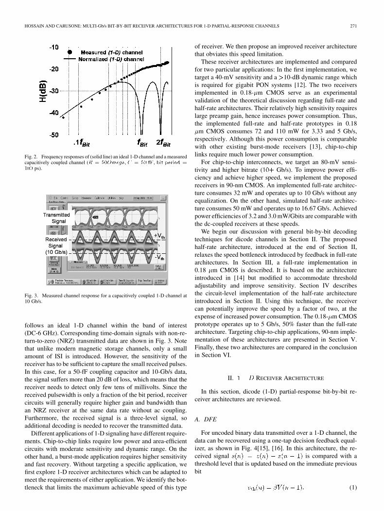
Measured and modeled responses of such an ac-coupledchannel are shown in Fig. 2 for a 50-fF coupling capacitorand 50- termination resistor. The channel suffers from 40 dBof loss at 0.05 and more than 15 dB of loss at 2.5 .The measured capacitively coupled channel response closely
1549-8328/$26.00 © 2010 IEEE
HOSSAIN AND CARUSONE: MULTI-Gb/s BIT-BY-BIT RECEIVER ARCHITECTURES FOR 1-D PARTIAL-RESPONSE CHANNELS 271
Fig. 2. Frequency responses of (solid line) an ideal 1-D channel and a measuredcapacitively coupled channel (� � �������, � � �� ��, ��� ��� �
��� ps).
Fig. 3. Measured channel response for a capacitively coupled 1-D channel at10 Gb/s.
follows an ideal 1-D channel within the band of interest(DC-6 GHz). Corresponding time-domain signals with non-re-turn-to-zero (NRZ) transmitted data are shown in Fig. 3. Notethat unlike modern magnetic storage channels, only a smallamount of ISI is introduced. However, the sensitivity of thereceiver has to be sufficient to capture the small received pulses.In this case, for a 50-fF coupling capacitor and 10-Gb/s data,the signal suffers more than 20 dB of loss, which means that thereceiver needs to detect only few tens of millivolts. Since thereceived pulsewidth is only a fraction of the bit period, receivercircuits will generally require higher gain and bandwidth thanan NRZ receiver at the same data rate without ac coupling.Furthermore, the received signal is a three-level signal, soadditional decoding is needed to recover the transmitted data.
Different applications of 1-D signaling have different require-ments. Chip-to-chip links require low power and area-efficientcircuits with moderate sensitivity and dynamic range. On theother hand, a burst-mode application requires higher sensitivityand fast recovery. Without targeting a specific application, wefirst explore 1-D receiver architectures which can be adapted tomeet the requirements of either application. We identify the bot-tleneck that limits the maximum achievable speed of this type
of receiver. We then propose an improved receiver architecturethat obviates this speed limitation.
These receiver architectures are implemented and comparedfor two particular applications: In the first implementation, wetarget a 40-mV sensitivity and a 10-dB dynamic range whichis required for gigabit PON systems [12]. The two receiversimplemented in 0.18- m CMOS serve as an experimentalvalidation of the theoretical discussion regarding full-rate andhalf-rate architectures. Their relatively high sensitivity requireslarge preamp gain, hence increases power consumption. Thus,the implemented full-rate and half-rate prototypes in 0.18
m CMOS consumes 72 and 110 mW for 3.33 and 5 Gb/s,respectively. Although this power consumption is comparablewith other existing burst-mode receivers [13], chip-to-chiplinks require much lower power consumption.
For chip-to-chip interconnects, we target an 80-mV sensi-tivity and higher bitrate ( Gb/s). To improve power effi-ciency and achieve higher speed, we implement the proposedreceivers in 90-nm CMOS. An implemented full-rate architec-ture consumes 32 mW and operates up to 10 Gb/s without anyequalization. On the other hand, simulated half-rate architec-ture consumes 50 mW and operates up to 16.67 Gb/s. Achievedpower efficiencies of 3.2 and 3.0 mW/Gbits are comparable withthe dc-coupled receivers at these speeds.
We begin our discussion with general bit-by-bit decodingtechniques for dicode channels in Section II. The proposedhalf-rate architecture, introduced at the end of Section II,relaxes the speed bottleneck introduced by feedback in full-ratearchitectures. In Section III, a full-rate implementation in0.18 m CMOS is described. It is based on the architectureintroduced in [14] but modified to accommodate thresholdadjustability and improve sensitivity. Section IV describesthe circuit-level implementation of the half-rate architectureintroduced in Section II. Using this technique, the receivercan potentially improve the speed by a factor of two, at theexpense of increased power consumption. The 0.18- m CMOSprototype operates up to 5 Gb/s, 50% faster than the full-ratearchitecture. Targeting chip-to-chip applications, 90-nm imple-mentation of these architectures are presented in Section V.Finally, these two architectures are compared in the conclusionin Section VI.
II. RECEIVER ARCHITECTURE
In this section, dicode (1-D) partial-response bit-by-bit re-ceiver architectures are reviewed.
A. DFE
For uncoded binary data transmitted over a 1-D channel, thedata can be recovered using a one-tap decision feedback equal-izer, as shown in Fig. 4[15], [16]. In this architecture, the re-ceived signal is compared with athreshold level that is updated based on the immediate previousbit
(1)

272 IEEE TRANSACTIONS ON CIRCUITS AND SYSTEMS—I: REGULAR PAPERS, VOL. 57, NO. 1, JANUARY 2010
Fig. 4. Dicode receiver using a DFE for symbol-by-symbol detection.
Fig. 5. 1-D partial-response signaling implemented with a precoder on thetransmitter side and a peak detector as a decoder on the receiver side.
A hardware-efficient implementation of this technique is dis-cussed in [3] and [4] where this functionality can be achieved athigh speed utilizing a hysteresis latch. Compared with a conven-tional decision feedback equalization (DFE), this architectureprovides several advantages: 1) Since there is no clock required,this architecture can be implemented with less complexity andlower power consumption and 2) since there is no delay flip–flopin the feedback path, it will settle faster than a clocked one-tapDFE. However, there is still a feedback path that must settle,and the highest achievable speed of this architecture is gener-ally also limited by the settling time of that loop which must beless than 1 UI.
B. Full-Rate Precoder and Decoder
A precoding method for 1-D partial-response channel is pro-posed in [1]. The precoder output is related to the data to betransmitted by
(2)
One possible architecture is shown in Fig. 5. A similar archi-tecture was presented for a duobinary (1-D) channel in [17] and,more recently, has been discussed in [18]. The decoder convertsthe three-level received signal to a two-level binary outputusing the following decision criteria:
(3)
(4)
This is accomplished using a conventional peak-detection re-ceiver shown in Fig. 5. It may be shown that, in the absence ofnoise causing decision errors, .
In some applications, such as burst-mode PON systems,where the transmitter does not provide the precoding function-ality, the precoder can be moved to the receiver side as shownin Fig. 6. The thresholds are chosen so that the receivedsignal amplitude only exceeds when there has been a
transition in the transmitted bit stream. [i.e., ].In this case
(5)
(6)
Hence, the output of the first XOR operation is
(7)
and the decoder output is
(8)
Using (7) and (8), the decoded output can be expressed asa function of the transmitted symbol
(9)
This equation can be iteratively extended back in time to the firsttransmitted symbol, which we shall assign to time
(10)
Thus, if the initial transmitted symbol and the initial de-coder output are the same, (10) reduces to ,and the decoder output is indeed equal to the transmitted data.Comparing the transceiver architectures in Figs. 4–6, the highestachievable speed is always limited by the delay of a feedbackloop which must be a 1-bit period or less.
C. Receiver With Half-Rate Decoder
To ease the settling-time requirements of all the previous ar-chitectures, we introduce the half-rate decoder shown in Fig. 7.This architecture is a natural progression from the one shown inFig. 6, where the feedback loop is shifted before the XOR opera-tion. The operation of the half-rate receiver in Fig. 7 is best un-derstood by recognizing that the top path, through and , isresponsible for receiving positive peaks in s, whereas the bottompath, through and , receives only the negative peaks in s.Every positive peak in s (corresponding to a rising edge of )must be followed by a negative peak (corresponding to a fallingedge of ). Hence, the top path can never be active in two con-secutive bit periods. Similarly, all negative peaks are followedby a positive peak, so the negative path is never active for two bitperiods in a row. Hence, the feedback loops have twice as longto settle, i.e., 2 UI. The front-end of the receiver is unchangedfrom Fig. 6, so (5) and (6) are still valid.
Now, the decoder output and can be written as
(11)
(12)
The full-rate decoded output is then related to andas follows:
(13)
(14)

HOSSAIN AND CARUSONE: MULTI-Gb/s BIT-BY-BIT RECEIVER ARCHITECTURES FOR 1-D PARTIAL-RESPONSE CHANNELS 273
Fig. 6. Modified 1-D partial-response receiver with the precoder moved to the receiver.
Fig. 7. Proposed half-rate receiver architecture for 1-D partial-response signaling.
Note that
(15)
Substituting (15) into (14)
(16)
(17)
similarly, can be written as
(18)
substituting (18) into (17) results in
(19)
Thus, the decoder can correctly recover the transmitted symbolif the initial decoder output and the initial transmitted
symbol are the same, , the same requirementobtained for the full-rate architecture in Fig. 6. Notice thatpulses are generated at whenever a rising (falling)edge is observed on the channel data . Hence, these signalscan be used as inputs to a phase detector in a conventionalclock-recovery loop. Alternatively, we use them to injectionlock an oscillator in the simulations of Section V.
In summary, present low-complexity 1-D decoders generallyinclude feedback loops which must settle in less than 1 UI. How-ever, this requirement can be relaxed by using the half-rate ar-chitecture proposed in Fig. 7. The remainder of this paper de-scribes a prototype of the half-rate decoder and compares it witha full-rate decoder in the same technology. Error propagationof such receivers is the same as a conventional DFE. Just as inDFE-based partial-response receivers, so long as a sufficientlylow bit error rate (BER) is maintained, there is no observabledegradation performance.
III. FULL-RATE BIT-BY-BIT DETECTION
The receiver architecture shown in Fig. 8(a) was introducedin [14]. Notice the linear amplifier in parallel with the hysteresislatch, which improves the receiver’s overall speed. With this inplace, the receiver’s speed is determined by the settling time ofthe hysteresis latch and the bandwidth of the preamplifier.
A. Implementation
In the hysteresis latch, the received signal is compared witha threshold level provided by a feedback path. The polarity ofthe threshold is determined by the most recently detected bit.The circuit used for this purpose in [8] is shown in Fig. 8(b).This circuit demonstrates hysteresis if the following conditionis satisfied:
(20)
where is the small-signal transconductance of the feedbackdifferential pair. In practice, to ensure operation in the pres-ence of noise and process variations, is made nominallygreater than two. In addition, to accommodate both large andsmall inputs, the threshold levels should be adjustable. How-ever, this simple circuit suffers from two main challenges. First,the critical output node is heavily loaded by the capacitance of
and the following stages which limits its settling time.To reduce the time constant at the critical nodes, cascode de-
vices were used. Due to this transistor stacking, VDD was in-creased to 2.5 V in a 0.13- m CMOS process. In this paper, thetime constant is improved within the process nominal VDD. Thesecond challenge with using the hysteresis circuit in Fig. 8(b) isthat adjusting the threshold level will also effect other aspectsof the design, such as its settling time. Hence, to provide pro-grammability, several copies of the circuit were operated in par-allel in [13].The proposed circuit is shown in Fig. 8(c). An ad-ditional differential pair is introduced in the latch which

274 IEEE TRANSACTIONS ON CIRCUITS AND SYSTEMS—I: REGULAR PAPERS, VOL. 57, NO. 1, JANUARY 2010
Fig. 8. (a) Receiver architecture from [14]. (b) Hysteresis latch from [8]. (c) Proposed hysteresis latch.
provides several advantages: First, note that the condition forhysteresis is now
(21)
Compared with the condition for the previous circuit in (22),there is additional flexibility to choose the gain of each stage,
and , to minimize the settling time. Second, alsoworks as a buffer between the critical node and the followingstages. Finally, this architecture also allows adjustment of thethreshold levels, as shown in Fig. 9(a).
In addition, note the use of a “split load” at the output [19] sothat the feedback is taken from the fast-settling node with lowimpedance, while the output is taken from the node with largerswing. Hence, the feedback-loop settling time is dominated bythe time constant , whereas the “output settling time”is dependent on the time constant . This allowsdesign flexibility and relaxes the tradeoff between speed, sen-sitivity, and noise immunity. Simulations of the hysteresis latchin Fig. 9(b) indicate that the split load improves the settling timeby 20% in this circuit. The targeted sensitivity of the receiveris a 40-mV differential input. The hysteresis comparator thresh-olds can be adjusted from 150 to 400 mV differential input. InPON applications, the receiver threshold can be adjusted basedon a training preamble which precedes each data burst.
A five-stage preamplifier providing 24-dB differential gain isused in front of the hysteresis latch. Budgeting 30 mW of powerfor the preamplifier, without inductive peaking, the achievedbandwidth is only 2.5 GHz, resulting in excessive data-depen-dent jitter. Hence, inductive peaking was used to extend thebandwidth to 3.5 GHz.
B. Experimental Results
A die photograph of the receiver front end is shown in Fig. 10.Measurements were made with a channel comprising an ap-proximately 3-ft long SMA cable and a 50-fF ac-coupling ca-
Fig. 9. Hysteresis latch simulations: (a) Threshold adjustments by changingItail. (b)–(c) Improvement of threshold and output settling time with resistorsplitting: (b) without resistor splitting and (c) with resistor splitting.
pacitor on-chip which, together with the 50- on-chip termi-nation, forms the high-pass filter characterized in Figs. 2 and3. The measured results are obtained with single-ended excita-tion only. The receiver’s dynamic range was tested by varyingthe input amplitude from 40 to 200 mV. For a 40-mV input,the threshold level was adjusted to 70 mV, and for a 180 mVinput, the threshold level was adjusted to 180 mV. The re-ceiver demonstrated error-free data recovery at 3.3 Gb/s for a

HOSSAIN AND CARUSONE: MULTI-Gb/s BIT-BY-BIT RECEIVER ARCHITECTURES FOR 1-D PARTIAL-RESPONSE CHANNELS 275
Fig. 10. Full-rate receiver die photograph in 0.18 �m CMOS.
Fig. 11. Measured output eye of the full-rate receiver at 3.3 Gb/s for differentinput amplitude (a) 40 mV (b) 200 mV.
pseudorandom binary sequence (PRBS) pattern at bothsignal amplitudes [Fig. 11(a) and (b)].
IV. HALF-RATE DETECTION
The speed of the architecture in Section III is limited by thefinite bandwidth of the preamplifier and the threshold settlingtime. To further increase the speed of the (1-D) partial-responsereceivers, the parallel half-rate architecture described in Sec-tion II is used. The block diagram of a CMOS implementa-tion of this architecture is shown in Fig. 13. The front end iscomposed of two major circuit blocks: a slicer and a toggleflip–flop (T-FF). The T-FF provides the feedback and XOR oper-ation shown in each path of Fig. 7. The circuit outputsand correspond to and in Fig. 7. These may beXORed to recover the full-rate data or further demultiplexed for
Fig. 12. Results for a PRBS � � � pattern: (a) A segment of the transmittedand recovered sequences and (b) BER bathtub plot.
digital decoding at a much slower rate. One possible implemen-tation is shown in Fig. 13, where recovered half-rate clock isused to further demultiplex and . These de-muxed bitstreams are then XORed at a half-rate to decode theeven and odd bitstreams. Half-rate clock can be recovered fromthe transition information provided by and .
A. Implementation
The first stage of the slicer is a differential difference am-plifier that compares the input with . The detected pulsesare then passed through five inductively peaked amplifier stagesproviding 26-dB gain. Fortunately, due to the half-rate architec-ture, lower bandwidth can be tolerated here than in the full-ratepreamplifier. Hence, the total current consumption is only 9mA from an 1.8-V supply for each amplifier chain providinga 2.2-GHz bandwidth.
High-speed T-FFs have been widely used as dividers in bothwireline and wireless applications. Conventional current-modelogic T-FFs employ two back-to-back D latches as shown inFig. 13(d). A typical implementation of the D latch is shownin Fig. 14(a). This type of T-FF exhibits self-oscillation whichallows it to operate as a high-frequency divider. A typical sensi-tivity curve is shown in Fig. 14(a). Unfortunately, noise aroundthe self-oscillation frequency can cause the output to toggleerroneously during periods when there is no transition in thereceived data, resulting in bit errors in the decoded sequence.Thus, self-oscillation in the T-FF must be avoided to use it as a

276 IEEE TRANSACTIONS ON CIRCUITS AND SYSTEMS—I: REGULAR PAPERS, VOL. 57, NO. 1, JANUARY 2010
Fig. 13. (a) Proposed half-rate receiver architecture. (b) Transition detector circuit. (c) Building block of the five-stage preamp (d) T-FF.
Fig. 14. (a) Conventional D latch and corresponding T-FF sensitivity. (b) Proposed D Latch and simulated T-FF sensitivity.
decoder in this application. In addition, the buffer is neededto drive a capacitive load without loading the latch nodes.
To alleviate both of these problems, we bring the bufferwithin the feedback loop as shown in Fig. 14(b). The gainof is easily made adjustable to allow variable latchingstrength and, hence, T-FF sensitivity. The modified architectureprovides frequency-independent sensitivity characteristics, asshown in Fig. 14(b). Furthermore, stage effectively buffersthe critical latch node and eliminates the requirement of anadditional buffer.
Thus, the proposed latch circuit does not consume additionalpower compared with a conventional latch implementation.
B. Experimental Results
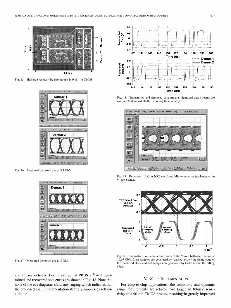
A prototype receiver in 0.18- m CMOS is shown in Fig. 15.In this implementation, we used the same 50-fF coupling capac-itor and 50- resistance as a high-pass filter to provide the 1-Dpartial response. The receiver provided error-free operation fora PRBS pattern up to 5 Gbits/s. Eye diagrams of thedemultiplexed outputs at 3.33 and 5 Gb/s are shown in Figs. 16
HOSSAIN AND CARUSONE: MULTI-Gb/s BIT-BY-BIT RECEIVER ARCHITECTURES FOR 1-D PARTIAL-RESPONSE CHANNELS 277
Fig. 15. Half-rate receiver die photograph in 0.18-�m CMOS.
Fig. 16. Measured demuxed eye at 3.3 Gb/s.
Fig. 17. Measured demuxed eye at 5 Gb/s.
and 17, respectively. Portions of actual PRBS trans-mitted and recovered sequences are shown in Fig. 18. Note thatnone of the eye diagrams show any ringing which indicates thatthe proposed T-FF implementation strongly suppresses self-os-cillation.
Fig. 18. Transmitted and demuxed data streams: demuxed data streams areoverlaid to demonstrate the decoding functionality.
Fig. 19. Recovered 10 Gb/s NRZ eye from full-rate receiver implemented in90-nm CMOS.
Fig. 20. Transistor level simulation results of the 90-nm half-rate receiver at16.67 Gb/s. Even samples are generated by (dashed arrow) the rising edge ofthe recovered clock and odd samples are generated by (solid arrow) the fallingedge.
V. 90-nm IMPLEMENTATION
For chip-to-chip applications, the sensitivity and dynamicrange requirements are relaxed. We target an 80-mV sensi-tivity in a 90-nm CMOS process resulting in greatly improved
278 IEEE TRANSACTIONS ON CIRCUITS AND SYSTEMS—I: REGULAR PAPERS, VOL. 57, NO. 1, JANUARY 2010
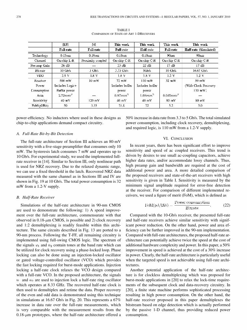
TABLE ICOMPARISON OF STATE-OF-ART 1-DRECEIVERS
power-efficiency. No inductors where used in these designs aschip-to-chip applications demand compact circuitry.
A. Full-Rate Bit-by-Bit Detection
The full-rate architecture of Section III achieves an 80-mVsensitivity with a five-stage preamplifier that consumes only 10mW. The hysteresis latch consumes 7 mW and operates up to10 Gb/s. For experimental study, we used the implemented full-rate receiver in [14]. Similar to Section III, only nonlinear pathis used for NRZ recovery. Due to the relaxed dynamic range,we can use a fixed threshold in the latch. Recovered NRZ datameasured with the same channel as in Sections III and IV areshown in Fig. 19 at 10 Gb/s. The total power consumption is 32mW from a 1.2-V supply.
B. Half-Rate Receiver
Simulations of the half-rate architecture in 90-nm CMOSare used to demonstrate the following: 1) A speed improve-ment over the full-rate architecture, commensurate with thatobserved in 0.18- m CMOS, is possible and 2) clock recoveryand 1:2 demultiplexing is readily feasible within this archi-tecture. The same circuits described in Fig. 13 are ported to a90-nm process. Following the T-FF, all remaining circuitry isimplemented using full-swing CMOS logic. The spectrum ofthe signals and contain tones at the baud rate which canbe utilized for clock recovery using a phase-locked loop. Phaselocking can also be done using an injection-locked oscillatoror gated voltage-controlled oscillator (VCO) which providesthe fast locking required for burst-mode applications. Injectionlocking a half-rate clock relaxes the VCO design comparedwith a full-rate VCO. In the proposed architecture, the signals
and are used to injection lock a half-rate ring oscillatorwhich operates at 8.33 GHz. The recovered half-rate clock isthen used to demultiplex and retime the data. Proper recoveryof the even and odd data is demonstrated using this techniquein simulations at 16.67 Gb/s in Fig. 20. This represents a 67%increase in data rate over the full-rate measurements, whichis very comparable with the measurement results from the0.18- m prototypes, where the half-rate architecture offered a
50% increase in data rate from 3.3 to 5 Gb/s. The total simulatedpower consumption, including clock recovery, demultiplexing,and required logic, is 110 mW from a 1.2-V supply.
VI. CONCLUSION
In recent years, there has been significant effort to improvesensitivity and speed of ac coupled receivers. This trend isdriven by desires to use small ac-coupling capacitors, achievehigher data rates, and/or accommodate lossy channels. Thus,high preamp gain and bandwidth are required at the cost ofadditional power and area. A more detailed comparison ofthe proposed receivers and state-of-the-art receivers with highsensitivity is given in Table I. Sensitivity is measured by theminimum signal amplitude required for error-free detectionat the receiver. For comparison of different implemented re-ceivers, we used a figure of merit (FoM), which is defined as
(22)
Compared with the 10-Gb/s receiver, the presented full-rateand half-rate receivers achieve similar sensitivity with signif-icant power reduction. On the other hand, power and area ef-ficiency can be further improved in the 90-nm implementation.Compared with full-rate architectures, the proposed half-rate ar-chitecture can potentially achieve twice the speed at the cost ofadditional hardware complexity and power. In this paper, a 50%improvement in speed is achieved at the cost of a 30% increasein power. Clearly, the half-rate architecture is particularly usefulwhen the targeted speed is not achievable using full-rate archi-tectures.
Another potential application of the half-rate architec-ture is for clockless demultiplexing which was proposed forburst-mode applications in [20] to relax the lock-time require-ments of the subsequent clock and data-recovery circuitry. In[20], a finite state machine performs sophisticated processingresulting in high power consumption. On the other hand, thehalf-rate receiver proposed in this paper demultiplexes thebitstream based on edge detection which is actually performedby the passive 1-D channel, thus providing reduced powerconsumption.

HOSSAIN AND CARUSONE: MULTI-Gb/s BIT-BY-BIT RECEIVER ARCHITECTURES FOR 1-D PARTIAL-RESPONSE CHANNELS 279
ACKNOWLEDGMENT
The authors would like to thank CMC for providing the fab-rication facilities.
REFERENCES
[1] M. Kobayashi and D. T. Tang, “Application of partial-response channelcoding to magnetic recording systems,” IBM J. Res. Develop., vol. 14,no. 4, pp. 368–375, Jul. 1970.
[2] J. Benham, R. Amirtharajah, J. L. Critchlow, T. Simon, and T. F.Knight, Jr., “An alignment insensitive separable electromagnetic cou-pler for high-speed digital multidrop bus applications,” IEEE Trans.Microw. Theory Tech., vol. 51, no. 12, pp. 2597–2603, Dec. 2003.
[3] R. Drost, R. Hopkins, R. Ho, and I. Sutherland, “Proximity commu-nication,” IEEE J. Solid-State Circuits, vol. 39, no. 9, pp. 1529–1535,Sep. 2004.
[4] L. Luo, J. M. Wilson, S. E. Mick, J. Xu, L. Zhang, and P. D. Franzon,“A 3 Gb/s AC coupled chip-to-chip communication using a low swingpulse receiver,” in Proc. IEEE ISSCC Dig. Tech. Papers, Feb. 2005, pp.522–523.
[5] A. Fazzi, R. Canegallo, L. Ciccarelli, L. Magagni, F. Natali, E. Jung,P. L. Rolandi, and R. Guerrieri, “3D capacitive interconnections withmono- and bidirectional capabilities,” in Proc. IEEE ISSCC Dig. Tech.Papers, Feb. 2007, pp. 356–357.
[6] Q. Gu, Z. Xu, J. Ko, and M.-C. F. Chang, “Two 10 Gb/s/pin low-powerinterconnect methods for 3-D ICs,” in Proc. IEEE ISSCC Dig. Tech.Papers, Feb. 2007, pp. 448–449.
[7] C. Culurciello and A. G. Andreou, “Capacitive inter-chip data andpower transfer for 3-D VLSI,” IEEE Trans. Circuits Syst. II, Exp.Briefs, vol. 53, no. 12, pp. 1348–1352, Dec. 2006.
[8] M. Nogawa, K. Nishimura, S. Kimura, T. Yoshida, T. Kawamura, M.Togashi, K. Kumozaki, and Y. Ohtomo, “A 10 Gb/s burst-mode CDRIC in 0.13 �m CMOS,” in Proc. ISSCC Dig. Tech. Papers, Feb. 2005,pp. 228–229.
[9] G. D. Forney, “Maximum-likelihood sequence estimation of digital se-quences in the presence of intersymbol interference,” IEEE Trans. Inf.Theory, vol. IT-18, no. 3, pp. 363–378, May 1972.
[10] K. Kanda, D. Antono, K. Ishida, H. Kawaguchi, T. Kuroda, and T.Sakura, “1.27 Gb/s/pin 3 mW/pin wireless superconnect (WSC) inter-face scheme,” in Proc. IEEE ISSCC Dig. Tech. Papers, Feb. 2003, pp.186–187.
[11] N. Miura, Y. Kohama, Y. Sugimori, H. Ishikuro, T. Sakurai, and T.Kuroda, “An 11 Gb/s inductive-coupling link with burst transmission,”in Proc. IEEE ISSCC Dig. Tech. Papers, Feb. 2008, pp. 298–290.
[12] T. Nakanishi, K-I. Suzuki, Y. Fukada, N. Yoshimoto, M. Nakamura,K. Kato, K. Nishimura, Y. Ohtomo, and M. Tsubokawa, “High sensi-tivity APD burst-mode receiver for 10 Gb/s TDM-PON system,” IEICEElectron. Express, vol. 4, no. 19, pp. 588–592, Oct. 2007.
[13] M. Nogawa, Y. Ohtomo, S. Kimura, K. Nishimura, T. Kawamura, andM. Togashi, “A 10 Gb/s burst-mode adaptive gain select limiting ampli-fier in 0.13 �m CMOS,” in Proc. ISSCC Dig. Tech. Papers, Feb. 2006,pp. 940–949.
[14] M. Hossain and A. C. Carusone, “A 14 Gb/s 32 mW AC coupled re-ceiver in 90-nm CMOS,” in Proc. VLSI Circuits Symp., Kyoto, Japan,Jun. 2007, pp. 32–33.
[15] R. W. Wood and R. W. Donaldson, “Decision feedback equalization ofthe DC null in high-density digital magnetic recording,” IEEE Trans.Magn., vol. MAG-14, no. 4, pp. 218–222, Jul. 1978.
[16] J. W. M. Bergmans, “Decision feedback equalization for digitalmagnetic recording systems,” IEEE Trans. Magn., vol. 24, no. 1, pp.683–688, Jan. 1988.
[17] J. H. Sinsky, A. Adamiecki, and M. Duelk, “10 Gb/s electrical back-plane transmission using duobinary signaling,” in Proc. IMS Dig. Tech.Papers, Jun. 2004, pp. 109–112.
[18] M. R. Ahmadi, J. Moon, and R. Harjani, “Constrained partial responsereceivers for high-speed links,” IEEE Trans. Circuits Syst. II, Exp.Briefs, vol. 55, no. 10, pp. 1006–1010, Oct. 2008.
[19] Y. M. Greshishchev and P. Schvan, “A 60 dB gain 55 dB dynamicrange 10 Gb/s broadband SiGe HBT limiting amplifier,” in Proc. IEEEISSCC Dig. Tech. Papers, Feb. 1999, pp. 382–383.
[20] B. Analui and A. Hajimiri, “Instantaneous clockless data recovery anddemultiplexing,” IEEE Trans. Circuits Syst. II, Exp. Briefs, vol. 52, no.8, pp. 437–441, Aug. 2005.
Masum Hossain received the B.Sc. degree in elec-trical engineering from Bangladesh University ofEngineering and Technology, Dhaka, Bangladesh, in2002 and the M.Sc. degree from Queen’s University,Kingston, ON, Canada, in 2005. During his M.Sc.,he worked on K-band wireless receiver in CMOS.Since 2005, he has been working toward the Ph.D.degree in electrical engineering at the University ofToronto, Toronto, Canada.
From September 2007 to January 2008, he waswith Intel Circuit Research Lab as a Graduate
Intern. Currently, he is with the Analog and Mixed Signal Division, GennumCorporation, Toronto. His research interest includes mixed-signal circuitsfor high-speed chip-to-chip communications, low power voltage-controlledoscillator, phase interpolator, and clock-recovery techniques.
Mr. Hossain won the Best Student Paper award in the 2008 IEEE CustomIntegrated Circuits Conference.
Anthony Chan Carusone (SM’96–M’02–S’08) re-ceived the B.A.Sc. and Ph.D. degrees from the Uni-versity of Toronto, Toronto, ON, Canada, in 1997 and2002, respectively.
In 2008, he was a Visiting Researcher with the Uni-versity of Pavia, Pavia, Italy, and later with the Cir-cuits Research Laboratory, Intel Corporation, Hills-boro, OR. Since 2001, he has been with the Depart-ment of Electrical and Computer Engineering, Uni-versity of Toronto, where he is currently an AssociateProfessor.
Prof. Carusone is a member and past Chair of the Analog Signal ProcessingTechnical Committee for the IEEE Circuits and Systems Society, a member andpast Chair of the Wireline Communications subcommittee of the Custom In-tegrated Circuits Conference, and an appointed member of the AdministrativeCommittee of the IEEE Solid-State Circuits Society. He has served as a GuestEditor for both the IEEE JOURNAL OF SOLID-STATE CIRCUITS and the IEEETRANSACTIONS ON CIRCUITS AND SYSTEMS I—REGULAR PAPERS. He is cur-rently Editor-in-Chief of the IEEE TRANSACTIONS ON CIRCUITS AND SYSTEMS
II—EXPRESS BRIEFS. While with the University of Toronto, he was the recip-ient of the Governor General’s Silver Medal. As a coauthor, he was the recipientof the Best Paper award at the 2005 Compound Semiconductor Integrated Cir-cuits Symposium and the Best Student Papers award at both the 2007 and 2008Custom Integrated Circuits Conferences.


![Med · 270 342 [(+72) (270+72) 472 (270+72 [(+72) tztžU +130) (+102)] (+130) 520 (270+250) 1270+102 752 (270+102 (+480) 750 270+480) 852 (270+102 (270+102](https://img.dokumen.tips/doc/110x75/5fb23750d464052f95224679/med-270-342-72-27072-472-27072-72-tztu-130-102-130-520-270250.jpg)