Embed Size (px)
Citation preview
CMP 112: PROGRAMMING ESSENTIALS, EDO UNIVERSITY, IYAMHO Page 1
I
COURSE CODE: PHY 213
COURSE TITLE: ELECTRIC CIRCUIT AND ELECTRONICS
NUMBER OF UNITS: 3 Units
COURSE DURATION: Three hours per week
COURSE LECTURER: ADEKOYA, MATHEW A
INTENDED LEARNING OUTCOMES
At the completion of this course, students are expected to:
1. Explain electric circuit and electronic
2. Mention all the different circuit theorem
3. Apply the concept to solve simple problems
4. Differentiate between N-type and P-type Semiconductor
5. Solve basic A.C problems
6. Design simple circuit.
COURSE DETAILS:
Week 1-2: Kirchhoff’s Laws
Week 3-5 Theorems ( Superposition Principle, thervenins, Norton, etc.)
Week 6-9: A.C Circuit
Week 10: Transformer Design,
Week 9-10 Semiconductor
Week 11: Oscillator
Week 12 Revision
RESOURCES
• Lecturer’s Office Hours:
• Mr. Adekoya, M.A Mondays 10:00-12:00pm.
• Mr. Adekoya, M.A, Wednesdays 2-3pm,
• Course lecture
• Books:
Fundamental of Electric Circuit by Alexander and Sadiku
Electrical and Electronics Principle and Technology by John Bird
•
: 0-12-369-446-9 (recommended).
CMP 112: PROGRAMMING ESSENTIALS, EDO UNIVERSITY, IYAMHO Page 2
Project:
• Homeworks + Project: ~ 30% of final grade.
• Exams:
• Final, comprehensive (according to university schedule): ~ 70% of final grade
Assignments & Grading
• Academic Honesty: All classwork should be done independently, unless explicitly stated otherwise
on the assignment handout.
• You may discuss general solution strategies, but must write up the solutions yourself.
• If you discuss any problem with anyone else, you must write their name at the top of your assignment,
labeling them “collaborators”.
• NO LATE HOMEWORKS ACCEPTED
• Turn in what you have at the time it’s due.
• All homeworks are due at the start of class.
• If you will be away, turn in the homework early.
• Late Programming Assignments (projects) will not be accepted, but penalized according to the
percentages given on the syllabus.
PREAMBLE:
D.C. CIRCUIT THEORY
The laws which determine the currents and voltage drops in d.c. networks are:
(a) Ohm’s law (b) the laws for resistors in series and in parallel and (c) Kirchhoff’s laws.
In addition, there are a number of circuit theorems which have been developed for solving problems in
electrical networks. These include:
(i) The superposition theorem (ii) Thévenin’s theorem
(iii) Norton’s theorem and
(iv) the maximum power transfer theorem
CIRCUIT DEFINITIONS
Node –a point of connection between two or more branches.
Branch – a single element such as voltage source or a resistor.
Loop – is any closed path in a circuit.
Example
How many nodes, branches & loops?
CMP 112: PROGRAMMING ESSENTIALS, EDO UNIVERSITY, IYAMHO Page 3
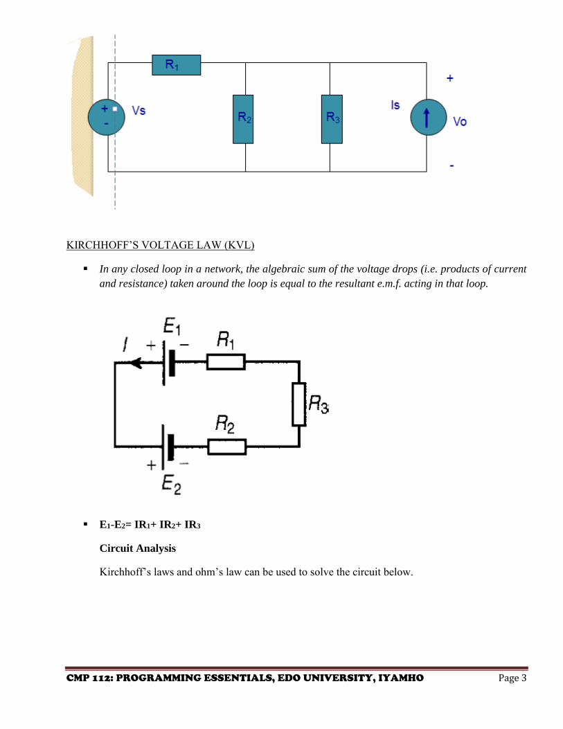
KIRCHHOFF’S VOLTAGE LAW (KVL)
In any closed loop in a network, the algebraic sum of the voltage drops (i.e. products of current
and resistance) taken around the loop is equal to the resultant e.m.f. acting in that loop.
E1-E2= IR1+ IR2+ IR3
Circuit Analysis
Kirchhoff’s laws and ohm’s law can be used to solve the circuit below.
CMP 112: PROGRAMMING ESSENTIALS, EDO UNIVERSITY, IYAMHO Page 4
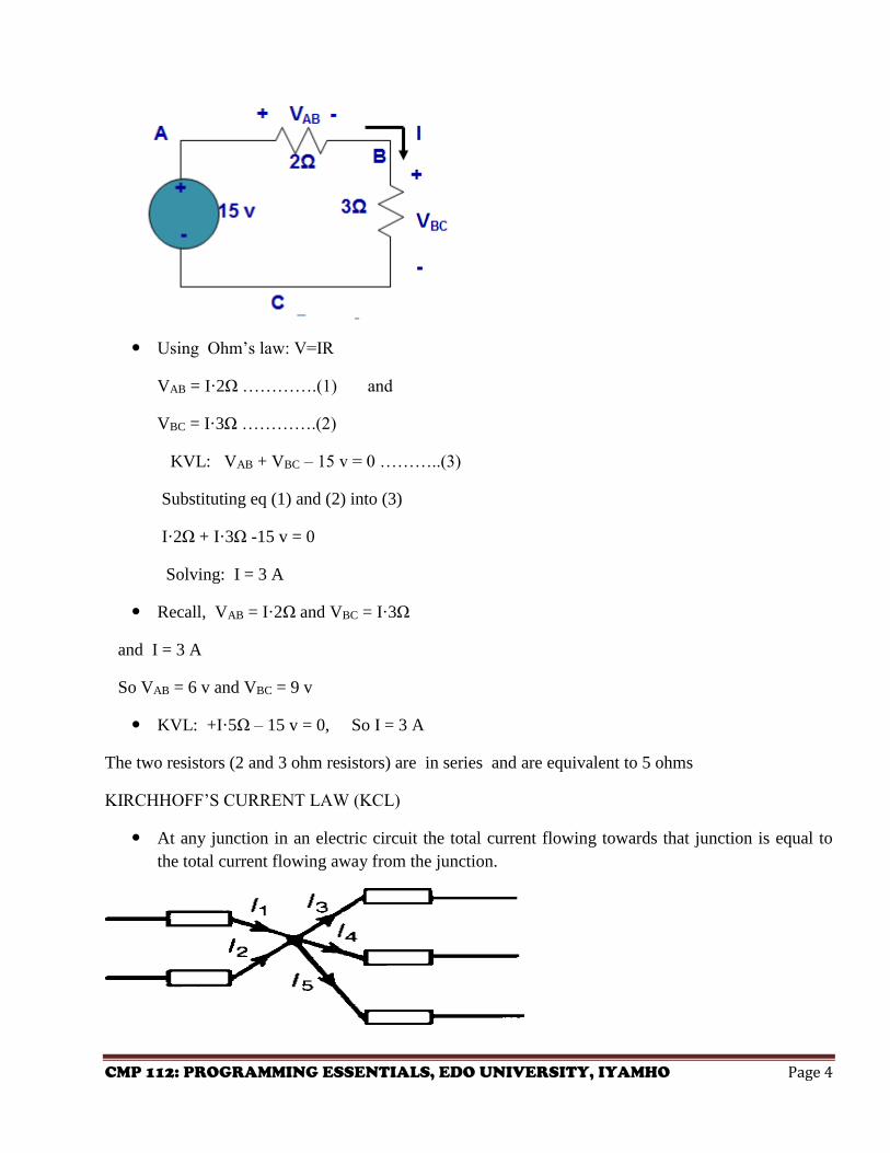
Using Ohm’s law: V=IR
VAB = I·2Ω ………….(1) and
VBC = I·3Ω ………….(2)
KVL: VAB + VBC – 15 v = 0 ………..(3)
Substituting eq (1) and (2) into (3)
I·2Ω + I·3Ω -15 v = 0
Solving: I = 3 A
Recall, VAB = I·2Ω and VBC = I·3Ω
and I = 3 A
So VAB = 6 v and VBC = 9 v
KVL: +I·5Ω – 15 v = 0, So I = 3 A
The two resistors (2 and 3 ohm resistors) are in series and are equivalent to 5 ohms
KIRCHHOFF’S CURRENT LAW (KCL)
At any junction in an electric circuit the total current flowing towards that junction is equal to
the total current flowing away from the junction.
CMP 112: PROGRAMMING ESSENTIALS, EDO UNIVERSITY, IYAMHO Page 5
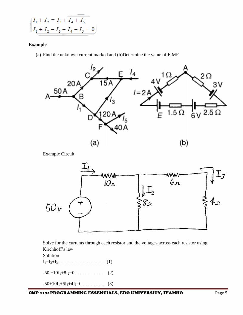
Example
(a) Find the unknown current marked and (b)Determine the value of E.MF
Example Circuit
Solve for the currents through each resistor and the voltages across each resistor using
Kirchhoff’s law
Solution
I1=I2+I3 …………………………(1)
-50 +10I1+8I2=0 ……………… (2)
-50+10I1+6I3+4I3=0 ………….. (3)
CMP 112: PROGRAMMING ESSENTIALS, EDO UNIVERSITY, IYAMHO Page 6
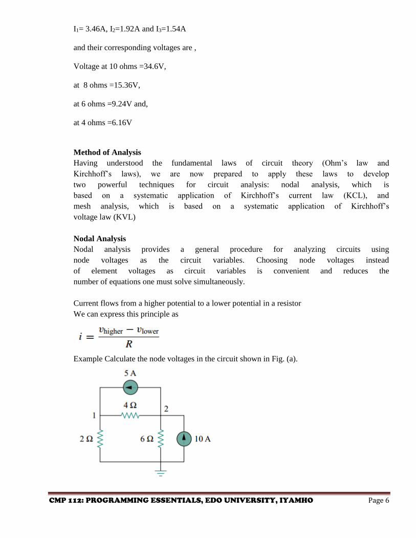
I1= 3.46A, I2=1.92A and I3=1.54A
and their corresponding voltages are ,
Voltage at 10 ohms =34.6V,
at 8 ohms =15.36V,
at 6 ohms =9.24V and,
at 4 ohms =6.16V
Method of Analysis
Having understood the fundamental laws of circuit theory (Ohm’s law and
Kirchhoff’s laws), we are now prepared to apply these laws to develop
two powerful techniques for circuit analysis: nodal analysis, which is
based on a systematic application of Kirchhoff’s current law (KCL), and
mesh analysis, which is based on a systematic application of Kirchhoff’s
voltage law (KVL)
Nodal Analysis
Nodal analysis provides a general procedure for analyzing circuits using
node voltages as the circuit variables. Choosing node voltages instead
of element voltages as circuit variables is convenient and reduces the
number of equations one must solve simultaneously.
Current flows from a higher potential to a lower potential in a resistor
We can express this principle as
Example Calculate the node voltages in the circuit shown in Fig. (a).
CMP 112: PROGRAMMING ESSENTIALS, EDO UNIVERSITY, IYAMHO Page 7
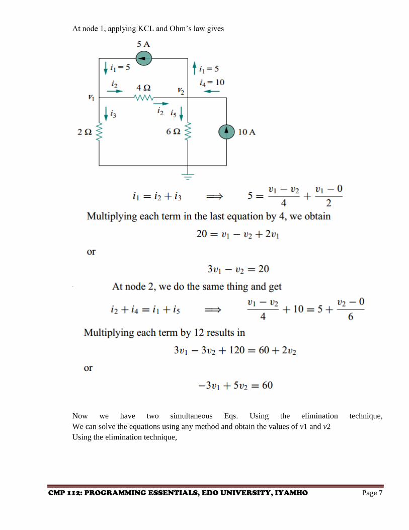
At node 1, applying KCL and Ohm’s law gives
Now we have two simultaneous Eqs. Using the elimination technique,
We can solve the equations using any method and obtain the values of v1 and v2
Using the elimination technique,
CMP 112: PROGRAMMING ESSENTIALS, EDO UNIVERSITY, IYAMHO Page 8
Mesh analysis
Mesh analysis provides another general procedure for analyzing circuits, using mesh currents as
the circuit variables. Using mesh currents instead of element currents as circuit variables is
convenient and reduces the number of equations that must be solved simultaneously. Recall that
a loop is a closed path with no node passed more than once. A mesh is a loop that does not
contain any other loop within it
A mesh is a loop which does not contain any other loops within it.
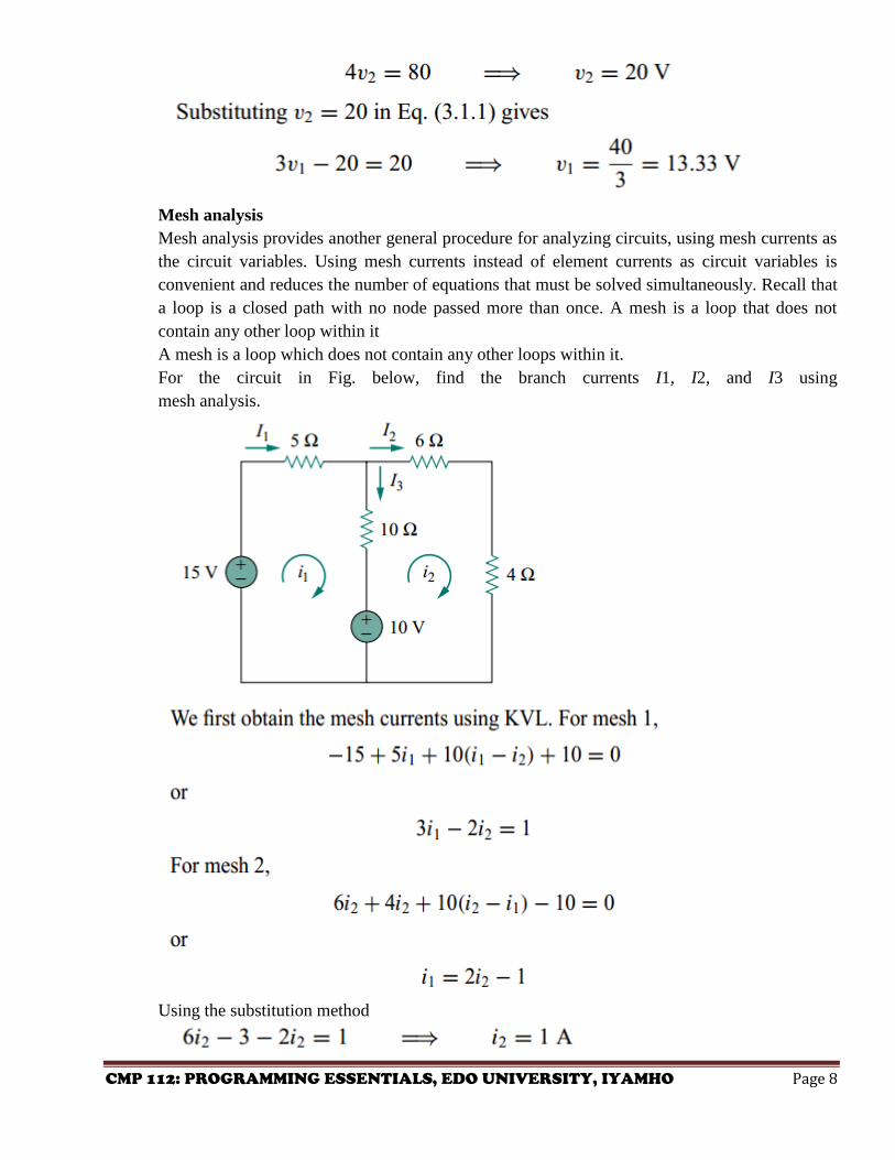
For the circuit in Fig. below, find the branch currents I1, I2, and I3 using
mesh analysis.
Using the substitution method
CMP 112: PROGRAMMING ESSENTIALS, EDO UNIVERSITY, IYAMHO Page 9
The superposition theorem
The superposition theorem states:
In any network made up of linear resistances and containing more than one source of e.m.f., the
resultant current flowing in any branch is the algebraic sum of the currents that would flow in
that branch if each source was considered separately, all other sources being replaced at that
time by their respective internal resistances.
Steps to Apply Superposition Principle
1. Turn off all independent sources except one source. Find the
output (voltage or current) due to that active source using nodal or mesh analysis.
2. Repeat step 1 for each of the other independent sources.
3. Find the total contribution by adding algebraically all the
contributions due to the independent sources.
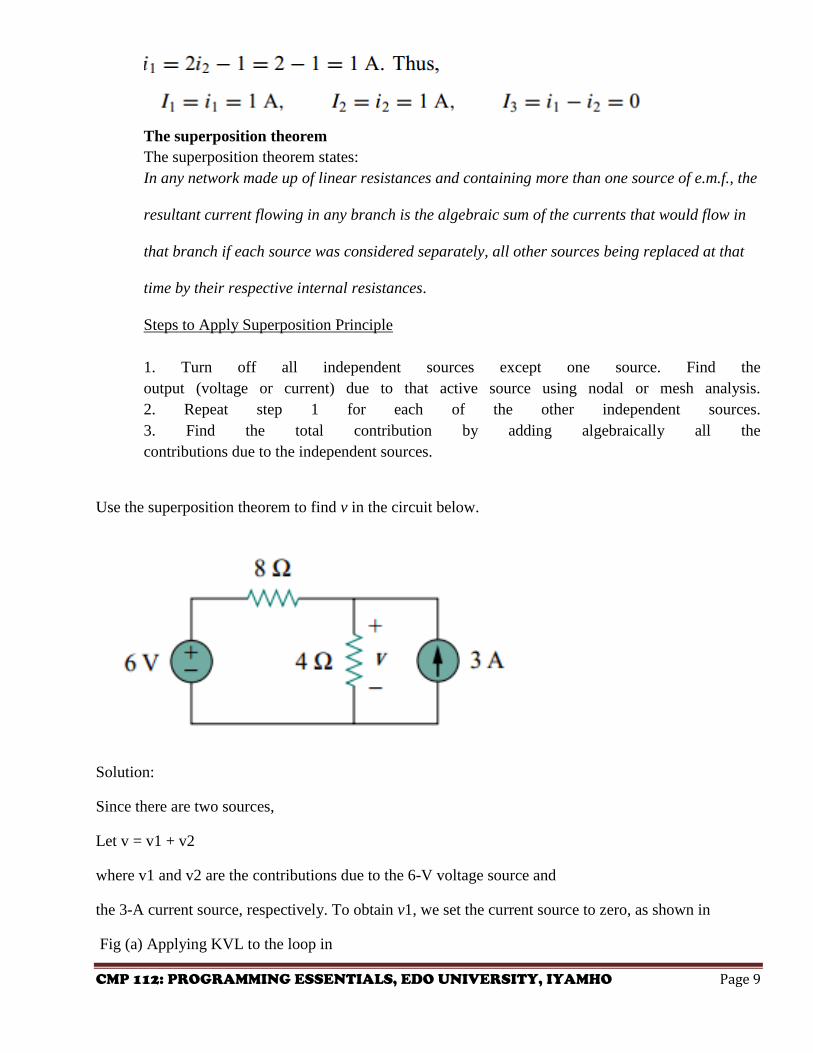
Use the superposition theorem to find v in the circuit below.
Solution:
Since there are two sources,
Let v = v1 + v2
where v1 and v2 are the contributions due to the 6-V voltage source and
the 3-A current source, respectively. To obtain v1, we set the current source to zero, as shown in
Fig (a) Applying KVL to the loop in
CMP 112: PROGRAMMING ESSENTIALS, EDO UNIVERSITY, IYAMHO Page 10
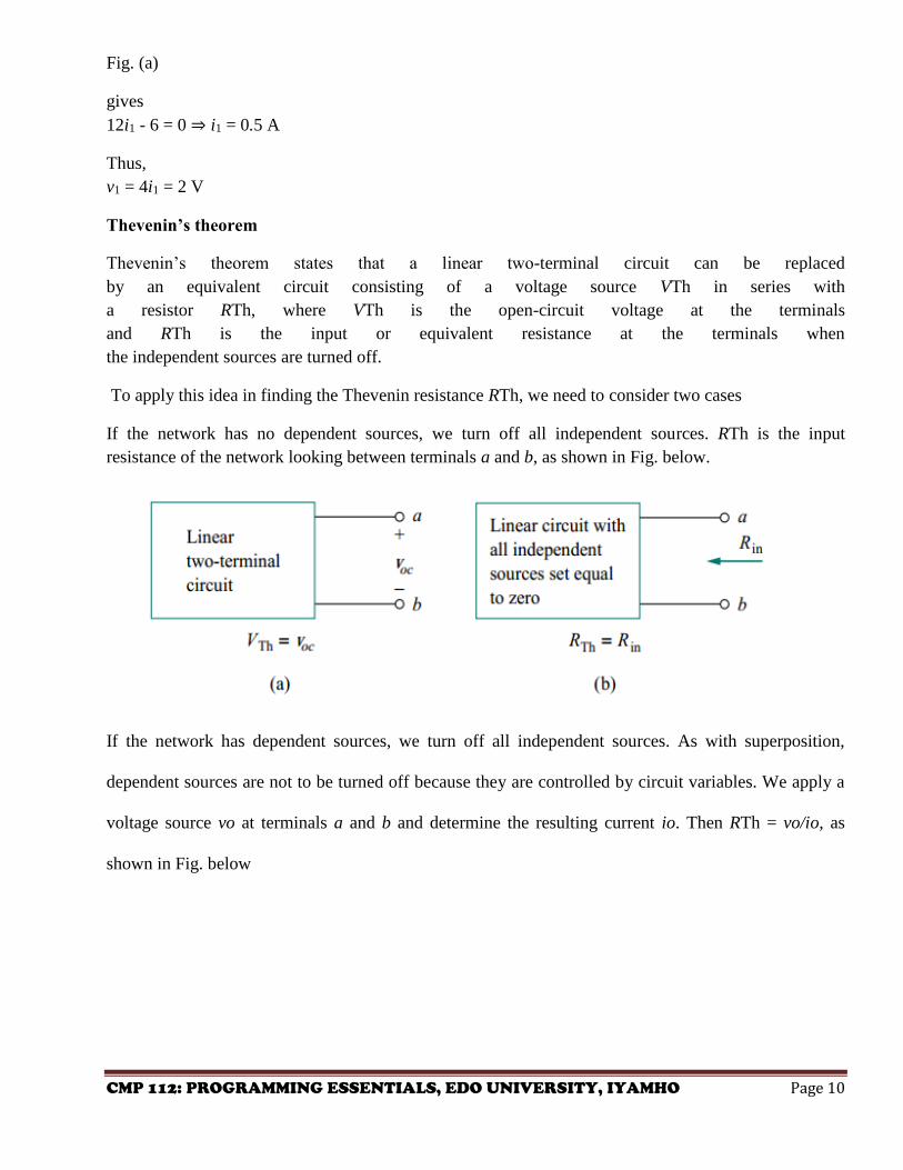
Fig. (a)
gives
12i1 - 6 = 0 ⇒ i1 = 0.5 A
Thus,
v1 = 4i1 = 2 V
Thevenin’s theorem
Thevenin’s theorem states that a linear two-terminal circuit can be replaced
by an equivalent circuit consisting of a voltage source VTh in series with
a resistor RTh, where VTh is the open-circuit voltage at the terminals
and RTh is the input or equivalent resistance at the terminals when
the independent sources are turned off.
To apply this idea in finding the Thevenin resistance RTh, we need to consider two cases
If the network has no dependent sources, we turn off all independent sources. RTh is the input
resistance of the network looking between terminals a and b, as shown in Fig. below.
If the network has dependent sources, we turn off all independent sources. As with superposition,
dependent sources are not to be turned off because they are controlled by circuit variables. We apply a
voltage source vo at terminals a and b and determine the resulting current io. Then RTh = vo/io, as
shown in Fig. below

CMP 112: PROGRAMMING ESSENTIALS, EDO UNIVERSITY, IYAMHO Page 11
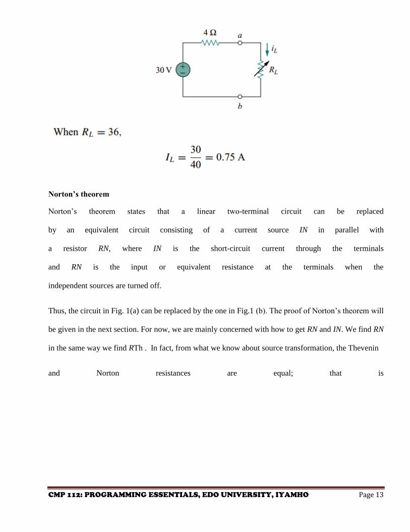
Thevenin equivalent of the circuit at the load’s
terminals is obtained, as shown in Fig. below, we obtain
Example:
Find the Thevenin equivalent circuit of the circuit shown in Fig. below, to the left of the terminals a-b.
Then find the current through RL = 6, 16, and 36 𝞨
We find RTh by turning off the 32-V voltage source (replacing it with a short circuit) and the 2-A
current source (replacing it with an open circuit). The circuit becomes what is shown in Fig. (a). Thus,
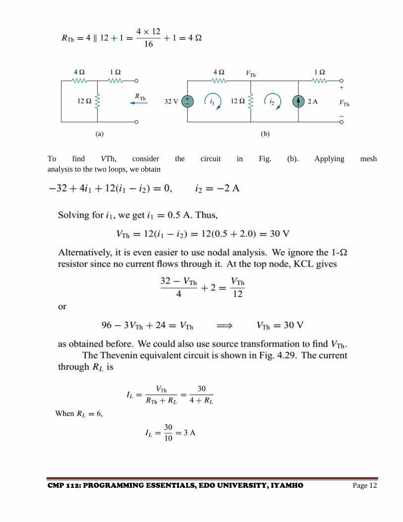
CMP 112: PROGRAMMING ESSENTIALS, EDO UNIVERSITY, IYAMHO Page 12
To find VTh, consider the circuit in Fig. (b). Applying mesh
analysis to the two loops, we obtain
CMP 112: PROGRAMMING ESSENTIALS, EDO UNIVERSITY, IYAMHO Page 13
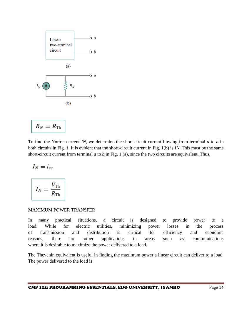
Norton’s theorem
Norton’s theorem states that a linear two-terminal circuit can be replaced
by an equivalent circuit consisting of a current source IN in parallel with
a resistor RN, where IN is the short-circuit current through the terminals
and RN is the input or equivalent resistance at the terminals when the
independent sources are turned off.
Thus, the circuit in Fig. 1(a) can be replaced by the one in Fig.1 (b). The proof of Norton’s theorem will
be given in the next section. For now, we are mainly concerned with how to get RN and IN. We find RN
in the same way we find RTh . In fact, from what we know about source transformation, the Thevenin
and Norton resistances are equal; that is
CMP 112: PROGRAMMING ESSENTIALS, EDO UNIVERSITY, IYAMHO Page 14
To find the Norton current IN, we determine the short-circuit current flowing from terminal a to b in
both circuits in Fig. 1. It is evident that the short-circuit current in Fig. 1(b) is IN. This must be the same
short-circuit current from terminal a to b in Fig. 1 (a), since the two circuits are equivalent. Thus,
MAXIMUM POWER TRANSFER
In many practical situations, a circuit is designed to provide power to a
load. While for electric utilities, minimizing power losses in the process
of transmission and distribution is critical for efficiency and economic
reasons, there are other applications in areas such as communications
where it is desirable to maximize the power delivered to a load.
The Thevenin equivalent is useful in finding the maximum power a linear circuit can deliver to a load.
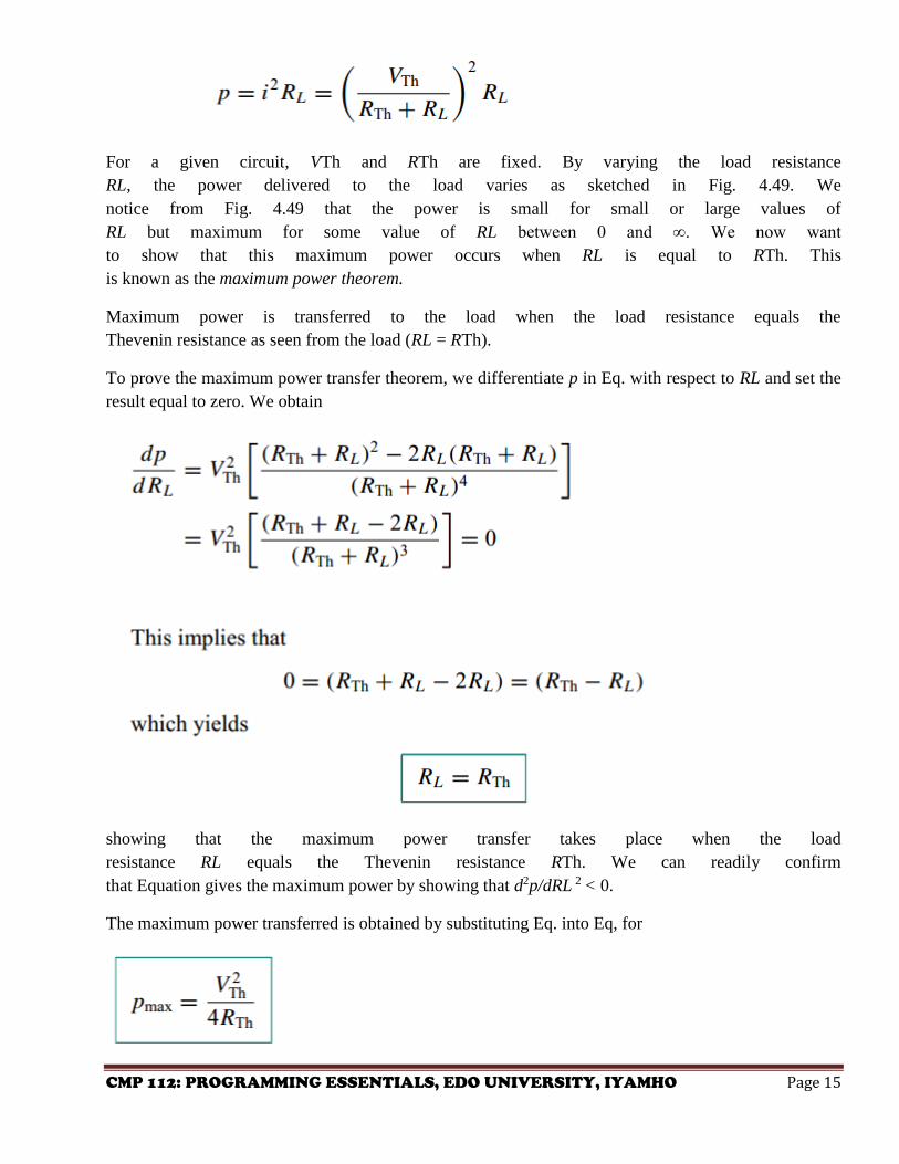
The power delivered to the load is
CMP 112: PROGRAMMING ESSENTIALS, EDO UNIVERSITY, IYAMHO Page 15
For a given circuit, VTh and RTh are fixed. By varying the load resistance
RL, the power delivered to the load varies as sketched in Fig. 4.49. We
notice from Fig. 4.49 that the power is small for small or large values of
RL but maximum for some value of RL between 0 and ∞. We now want
to show that this maximum power occurs when RL is equal to RTh. This
is known as the maximum power theorem.
Maximum power is transferred to the load when the load resistance equals the
Thevenin resistance as seen from the load (RL = RTh).
To prove the maximum power transfer theorem, we differentiate p in Eq. with respect to RL and set the
result equal to zero. We obtain
showing that the maximum power transfer takes place when the load
resistance RL equals the Thevenin resistance RTh. We can readily confirm
that Equation gives the maximum power by showing that d2p/dRL 2 < 0.
The maximum power transferred is obtained by substituting Eq. into Eq, for
CMP 112: PROGRAMMING ESSENTIALS, EDO UNIVERSITY, IYAMHO Page 16
Equation applies only when RL = RTh. When RL = RTh, we compute the power delivered to the load
using Eq..
Sources of EMF and Current
A source of electrical energy can be represented by a source of e.m.f. in series with a resistance. the
Thévenin constant-voltage source consisted of a constant e.m.f. E in series with an internal resistance r.
However this is not the only form of representation. A source of electrical energy can also be
represented by a constant-current source in parallel with a resistance. It may be shown that the two
forms are equivalent. An ideal constant-voltage generator is one with zero internal resistance so that it
supplies the same voltage to all loads. An ideal constant-current generator is one with infinite internal
resistance so that it supplies the same current to all loads.
Capacitor
A capacitor is a passive element designed to store energy in its electric
field. Besides resistors, capacitors are the most common electrical components. Capacitors are used
extensively in electronics, communications,
computers, and power systems. For example, they are used in the tuning
circuits of radio receivers and as dynamic memory elements in computer systems
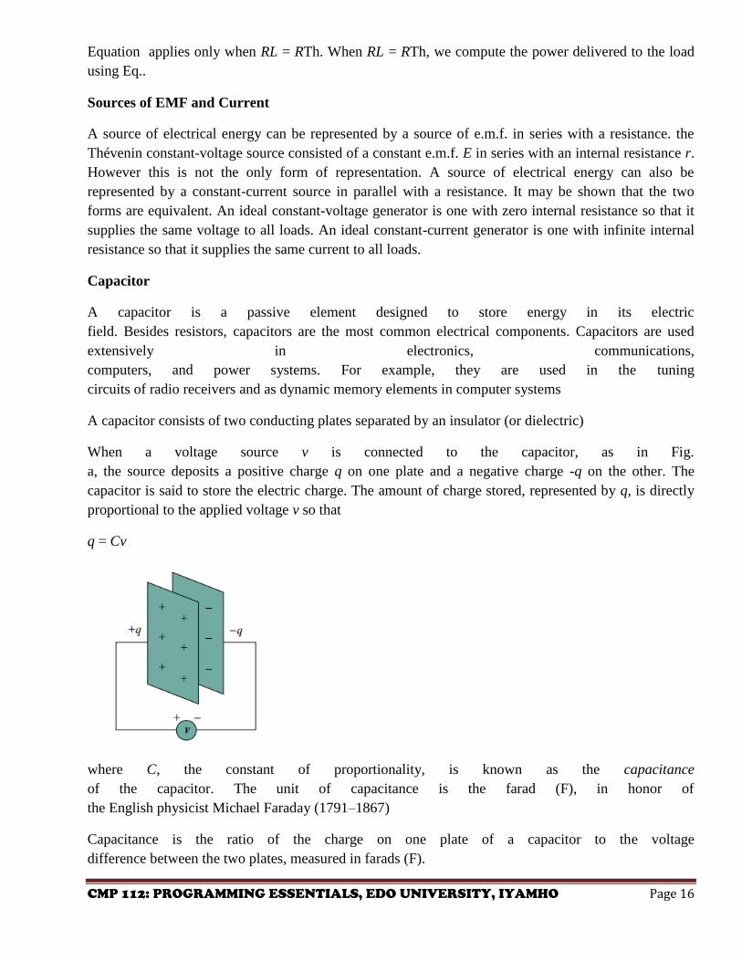
A capacitor consists of two conducting plates separated by an insulator (or dielectric)
When a voltage source v is connected to the capacitor, as in Fig.
a, the source deposits a positive charge q on one plate and a negative charge -q on the other. The
capacitor is said to store the electric charge. The amount of charge stored, represented by q, is directly
proportional to the applied voltage v so that
q = Cv
where C, the constant of proportionality, is known as the capacitance
of the capacitor. The unit of capacitance is the farad (F), in honor of
the English physicist Michael Faraday (1791–1867)
Capacitance is the ratio of the charge on one plate of a capacitor to the voltage
difference between the two plates, measured in farads (F).
CMP 112: PROGRAMMING ESSENTIALS, EDO UNIVERSITY, IYAMHO Page 17
Note: 1 farad = 1 coulomb/volt
Although the capacitance C of a capacitor is the ratio of the charge
q per plate to the applied voltage v, it does not depend on q or v. It
depends on the physical dimensions of the capacitor. For example, for
the parallel-plate capacitor, the capacitance is given by equation 2. as
where A is the surface area of each plate, d is the distance between the
plates, and is the permittivity of the dielectric material between the plates
The above Eq. applies to only parallel-plate capacitors,
may infer from it that, in general, three factors determine the value of the capacitance:
1. The surface area of the plates—the larger the area, the greater
the capacitance.
2. The spacing between the plates—the smaller the spacing, the
greater the capacitance.
3. The permittivity of the material—the higher the permittivity,
the greater the capacitance.
To obtain the current-voltage relationship of the capacitor, we take
the derivative of both sides of Eq. (1). Since
differentiating both sides, we have
This is the current-voltage relationship for a capacitor, assuming the positive sign convention
The voltage-current relation of the capacitor can be obtained by
integrating both sides of Eq.
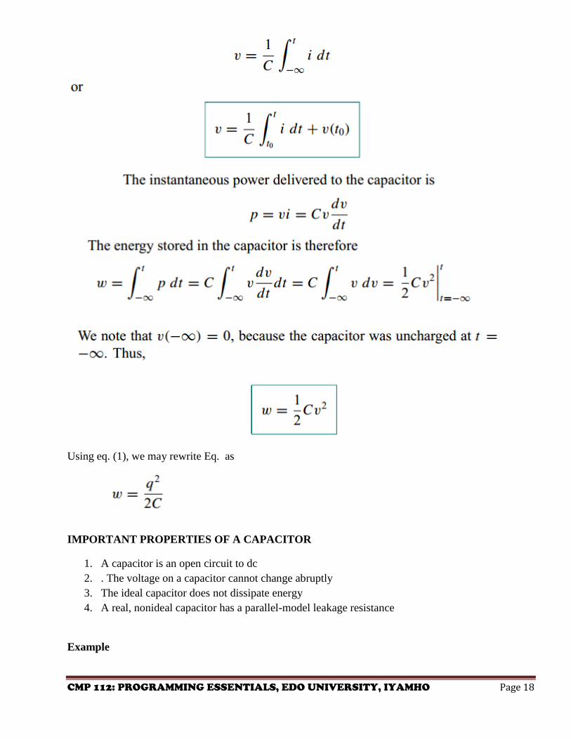
CMP 112: PROGRAMMING ESSENTIALS, EDO UNIVERSITY, IYAMHO Page 18
Using eq. (1), we may rewrite Eq. as
IMPORTANT PROPERTIES OF A CAPACITOR
1. A capacitor is an open circuit to dc
2. . The voltage on a capacitor cannot change abruptly
3. The ideal capacitor does not dissipate energy
4. A real, nonideal capacitor has a parallel-model leakage resistance
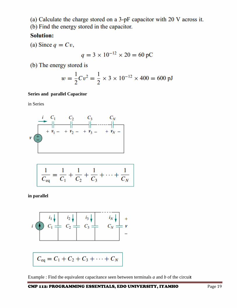
Example
CMP 112: PROGRAMMING ESSENTIALS, EDO UNIVERSITY, IYAMHO Page 19
Series and parallel Capacitor
in Series
in parallel
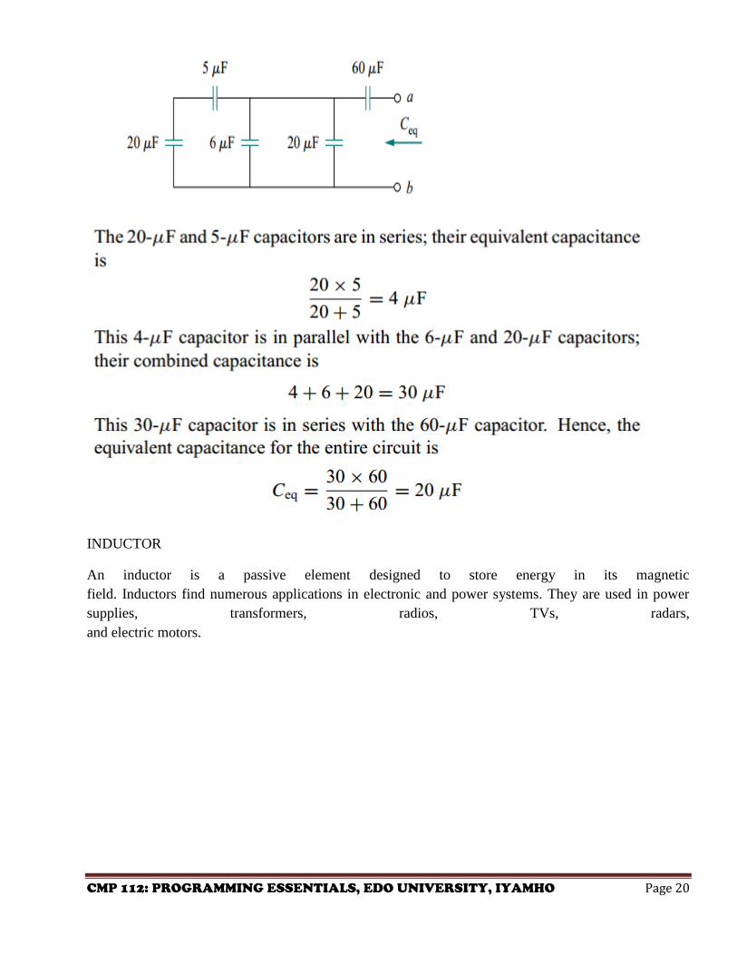
Example : Find the equivalent capacitance seen between terminals a and b of the circuit
CMP 112: PROGRAMMING ESSENTIALS, EDO UNIVERSITY, IYAMHO Page 20
INDUCTOR
An inductor is a passive element designed to store energy in its magnetic
field. Inductors find numerous applications in electronic and power systems. They are used in power
supplies, transformers, radios, TVs, radars,
and electric motors.
CMP 112: PROGRAMMING ESSENTIALS, EDO UNIVERSITY, IYAMHO Page 21
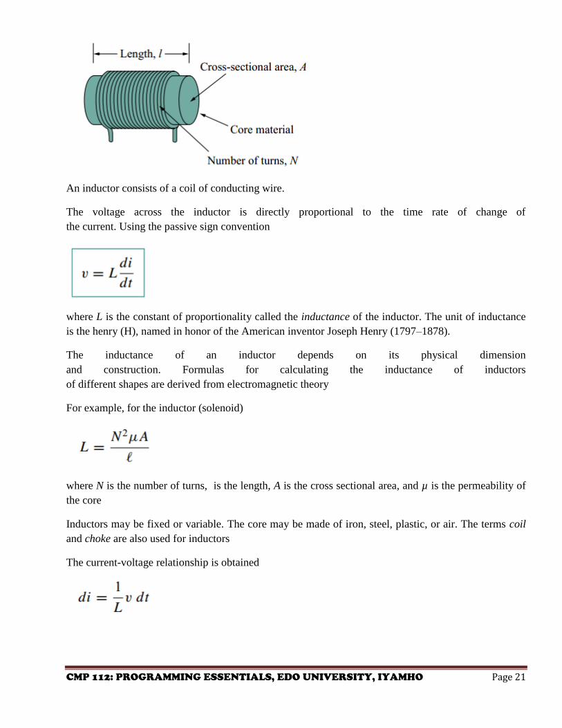
An inductor consists of a coil of conducting wire.
The voltage across the inductor is directly proportional to the time rate of change of
the current. Using the passive sign convention
where L is the constant of proportionality called the inductance of the inductor. The unit of inductance
is the henry (H), named in honor of the American inventor Joseph Henry (1797–1878).
The inductance of an inductor depends on its physical dimension
and construction. Formulas for calculating the inductance of inductors
of different shapes are derived from electromagnetic theory
For example, for the inductor (solenoid)
where N is the number of turns, is the length, A is the cross sectional area, and µ is the permeability of
the core
Inductors may be fixed or variable. The core may be made of iron, steel, plastic, or air. The terms coil
and choke are also used for inductors
The current-voltage relationship is obtained
CMP 112: PROGRAMMING ESSENTIALS, EDO UNIVERSITY, IYAMHO Page 22
The inductor is designed to store energy in its magnetic field. The energy stored can be obtained from
Eqs. above The power delivered to the inductor is
IMPORTANT PROPERTIES OF AN INDUCTOR
1. An inductor acts like a short circuit to dc.
2. The current through an inductor cannot change instantaneously
3. The ideal inductor does not dissipate energy
4. A practical, nonideal inductor has a significant resistive component
Series and Parallel Inductor
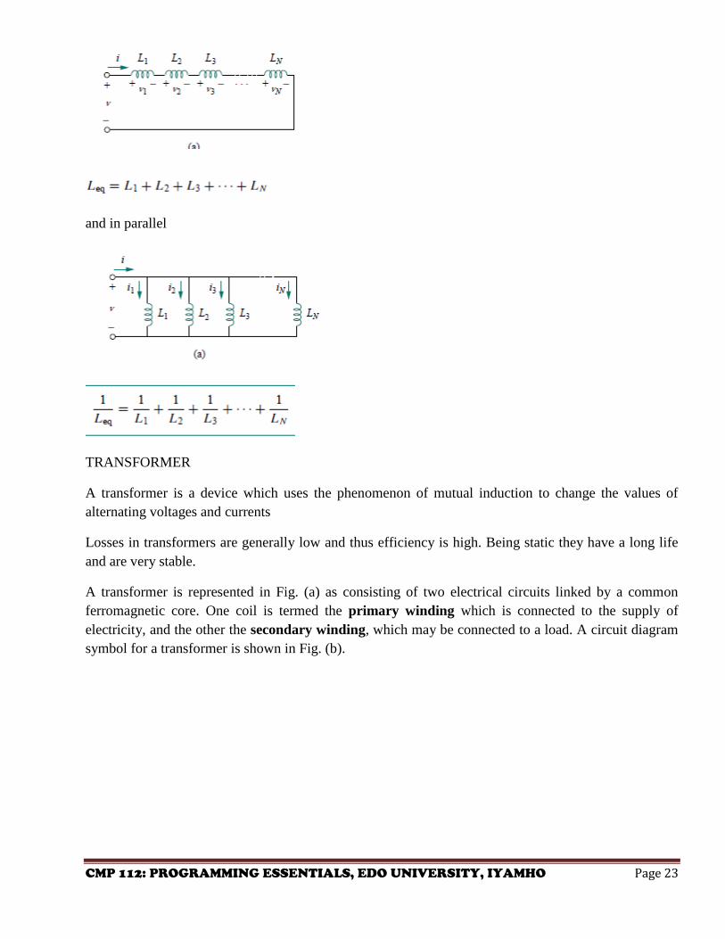
CMP 112: PROGRAMMING ESSENTIALS, EDO UNIVERSITY, IYAMHO Page 23
and in parallel
TRANSFORMER
A transformer is a device which uses the phenomenon of mutual induction to change the values of
alternating voltages and currents
Losses in transformers are generally low and thus efficiency is high. Being static they have a long life
and are very stable.
A transformer is represented in Fig. (a) as consisting of two electrical circuits linked by a common
ferromagnetic core. One coil is termed the primary winding which is connected to the supply of
electricity, and the other the secondary winding, which may be connected to a load. A circuit diagram
symbol for a transformer is shown in Fig. (b).

CMP 112: PROGRAMMING ESSENTIALS, EDO UNIVERSITY, IYAMHO Page 24
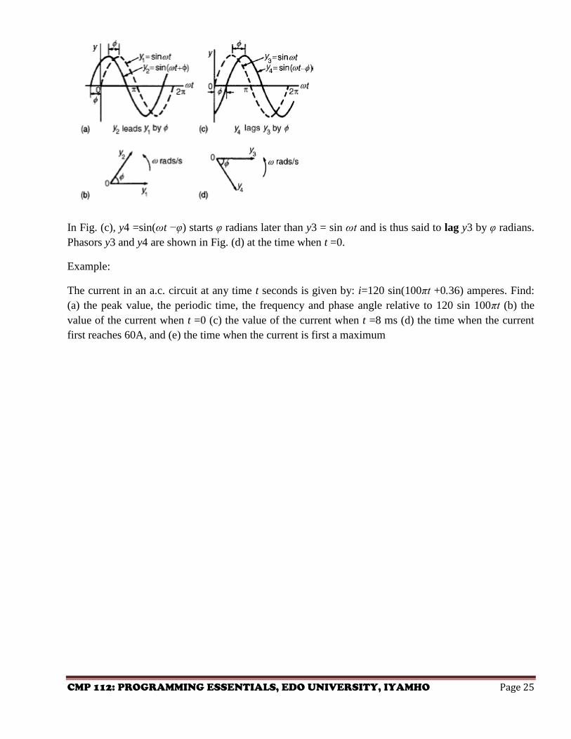
The equation of a sinusoidal waveform
0A represents a vector that is free to rotate anticlockwise about 0 at an angular velocity of ω rad/s. A
rotating vector is known as a phasor.
After time t seconds the vector 0A has turned through an angle ωt. If the line BC is constructed
perpendicular to 0A as shown, then
If all such vertical components are projected on to a graph of y against angle ωt (in radians), a sine
curve
results of maximum value 0A. Any quantity which varies sinusoidally can thus be represented as a
phasor. A sine curve may not always start at 0◦. To show this
a periodic function is represented by y=sin(ωt ±φ), where φ is the phase (or angle) difference compared
with y= sin ωt.
y2 =sin(ωt +φ) starts φ radians earlier than y1 = sin ωt and is thus said to lead y1 by φ radians. Phasors
y1 and y2 are shown fig .b in at the time when t =0.
CMP 112: PROGRAMMING ESSENTIALS, EDO UNIVERSITY, IYAMHO Page 25
In Fig. (c), y4 =sin(ωt −φ) starts φ radians later than y3 = sin ωt and is thus said to lag y3 by φ radians.
Phasors y3 and y4 are shown in Fig. (d) at the time when t =0.
Example:
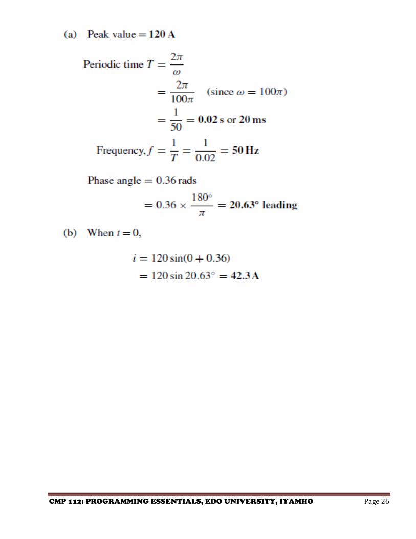
The current in an a.c. circuit at any time t seconds is given by: i=120 sin(100πt +0.36) amperes. Find:
(a) the peak value, the periodic time, the frequency and phase angle relative to 120 sin 100πt (b) the
value of the current when t =0 (c) the value of the current when t =8 ms (d) the time when the current
first reaches 60A, and (e) the time when the current is first a maximum
CMP 112: PROGRAMMING ESSENTIALS, EDO UNIVERSITY, IYAMHO Page 26
CMP 112: PROGRAMMING ESSENTIALS, EDO UNIVERSITY, IYAMHO Page 27
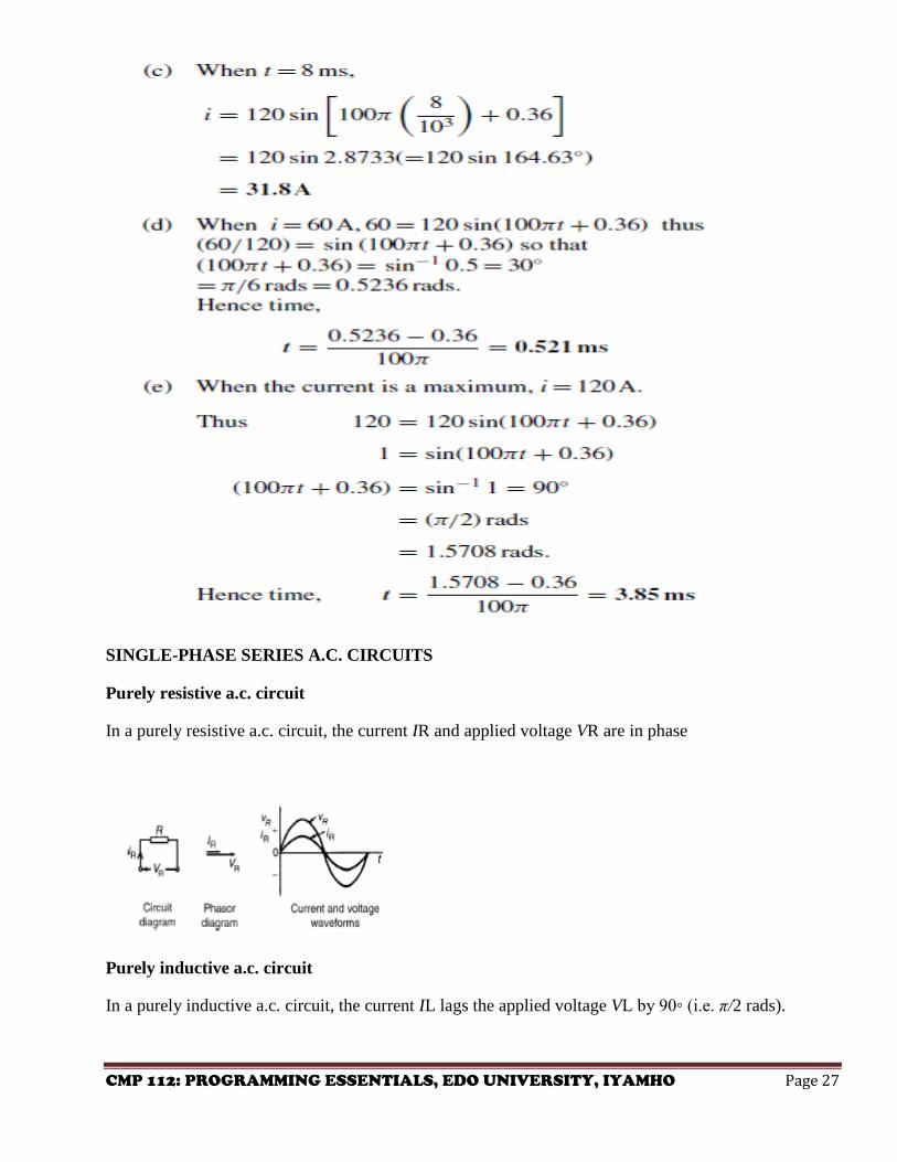
SINGLE-PHASE SERIES A.C. CIRCUITS
Purely resistive a.c. circuit
In a purely resistive a.c. circuit, the current IR and applied voltage VR are in phase
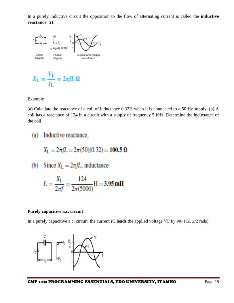
Purely inductive a.c. circuit
In a purely inductive a.c. circuit, the current IL lags the applied voltage VL by 90◦ (i.e. π/2 rads).
CMP 112: PROGRAMMING ESSENTIALS, EDO UNIVERSITY, IYAMHO Page 28
In a purely inductive circuit the opposition to the flow of alternating current is called the inductive
reactance, XL
Example
(a) Calculate the reactance of a coil of inductance 0.32H when it is connected to a 50 Hz supply. (b) A
coil has a reactance of 124 in a circuit with a supply of frequency 5 kHz. Determine the inductance of
the coil.
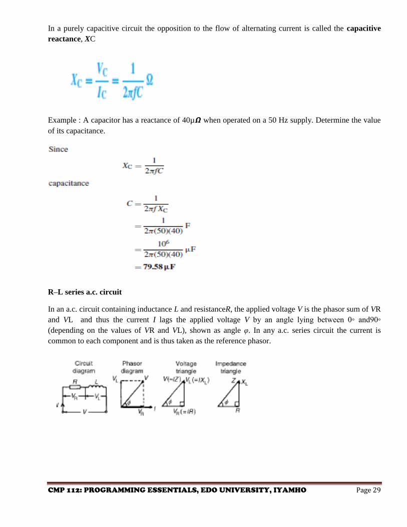
Purely capacitive a.c. circuit
In a purely capacitive a.c. circuit, the current IC leads the applied voltage VC by 90◦ (i.e. π/2 rads)
CMP 112: PROGRAMMING ESSENTIALS, EDO UNIVERSITY, IYAMHO Page 29
In a purely capacitive circuit the opposition to the flow of alternating current is called the capacitive
reactance, XC
Example : A capacitor has a reactance of 40µ𝞨 when operated on a 50 Hz supply. Determine the value
of its capacitance.
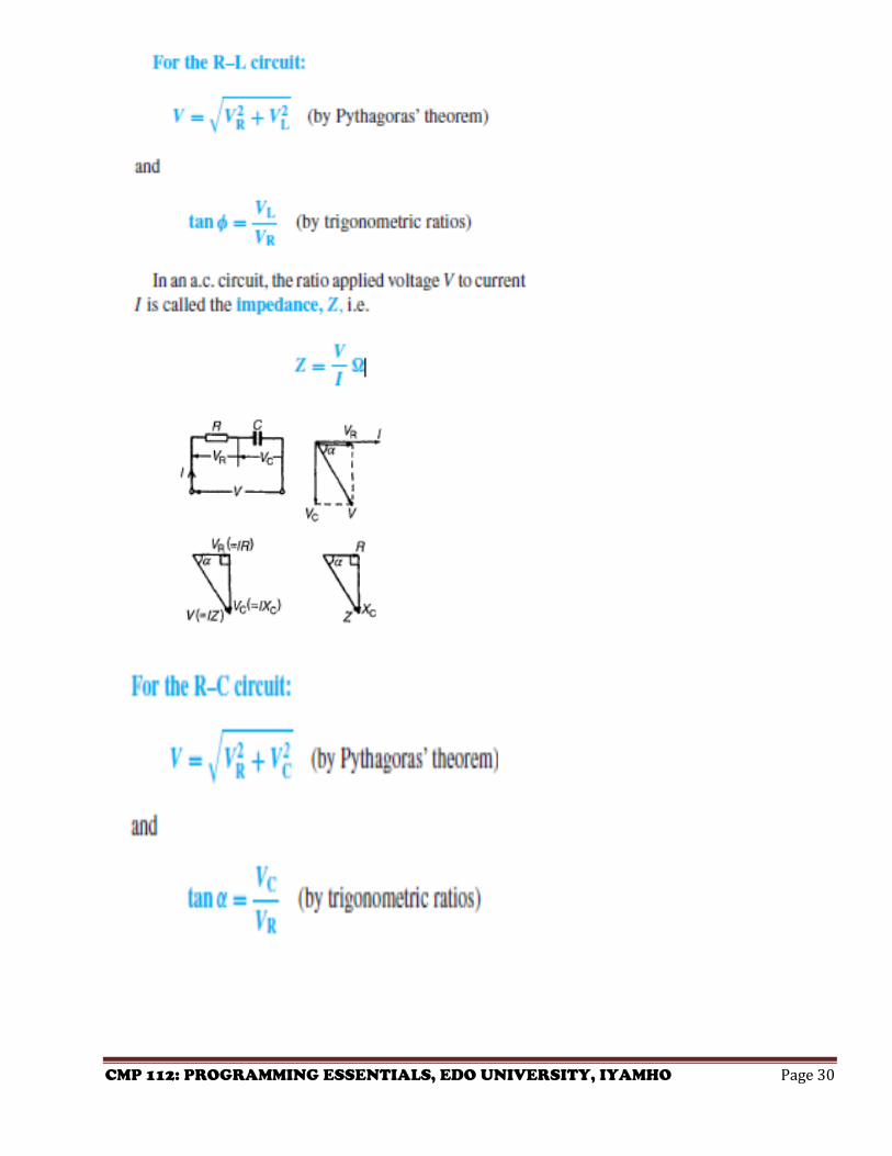
R–L series a.c. circuit
In an a.c. circuit containing inductance L and resistanceR, the applied voltage V is the phasor sum of VR
and VL and thus the current I lags the applied voltage V by an angle lying between 0◦ and90◦
(depending on the values of VR and VL), shown as angle φ. In any a.c. series circuit the current is
common to each component and is thus taken as the reference phasor.
CMP 112: PROGRAMMING ESSENTIALS, EDO UNIVERSITY, IYAMHO Page 30
CMP 112: PROGRAMMING ESSENTIALS, EDO UNIVERSITY, IYAMHO Page 31
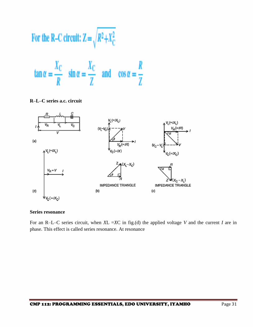
R–L–C series a.c. circuit
Series resonance
For an R–L–C series circuit, when XL =XC in fig.(d) the applied voltage V and the current I are in
phase. This effect is called series resonance. At resonance
CMP 112: PROGRAMMING ESSENTIALS, EDO UNIVERSITY, IYAMHO Page 32
FILTER
A filter is a network designed to pass signals having frequencies within certain bands (called
passbands) with little attenuation, but greatly attenuates signals within other bands (called attenuation
bands or stopbands). A filter is frequency sensitive and is thus composed of reactive elements. Since
certain frequencies are to be passed with minimal loss, ideally the inductors and capacitors need to be
pure components since the presence of resistance results in some attenuation at all frequencies.
Between the pass band of a filter, where ideally the attenuation is zero, and the attenuation band, where
ideally the attenuation is infinite, is the cut-off frequency, this being the frequency at which the
attenuation changes from zero to some finite value. A filter network containing no source of power is
termed passive, and one containing one or more power sources is known as an active filter network.
Filters are used for a variety of purposes in nearly every type of electronic communications and control
equipment. The bandwidths of filters used in communications systems vary from a fraction of a hertz to
many megahertz, depending on the application. There are four basic types of filter sections:
(a) low-pass
(b) high-pass
(c) band-pass
(d) band-stop
Semiconductor
Semiconductors are a group of materials having conductivities between those of metals and insulators
CMP 112: PROGRAMMING ESSENTIALS, EDO UNIVERSITY, IYAMHO Page 33
Two general classifications of semiconductors are the elemental semiconductor materials, found in
group IV of the periodic table, and the compound semiconductor materials, most of which are formed
from special combinations of group I11 and group V elements.
Intrinsic and Extrinsic Semiconductor
Intrinsic Semiconductor : Pure semiconductor
Extrinsic Semiconductor : Are semiconductor that have been doped either by penta- valent atom or tri-
valent atom.
Doping is an addition of impurity to a semiconductor.
The charge carrier in a semiconductors are hole (+) and electron (-).
Transistors
Transistors are capable of serving as switches and amplifiers, depending upon their configuration. The
term "transistor" comes from "transfer resistor" and alludes to a transistor's behavior as a resistor that
amplifies signals as they are transferred from the input to the output terminal of the device.
Transistors can be classified in two major categories: they can be either bipolar transistors or field
effect transistors. Each is fundamentally different from the other in its operation mechanisms. A bipolar
transistor operates through the injection and collection of minority carriers utilizing p-n junctions . By
contrast, a field effect transistor is a majority carrier device and is thus a unipolar device.
Operating Amplifier
An operation amplifier (OP-Amp) is a circuit that can perform such mathematics operations as addition,
subtraction, integration and differentiation.
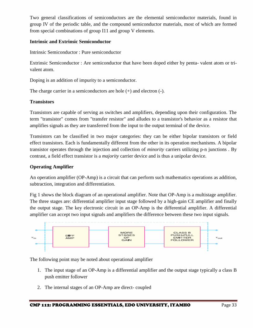
Fig 1 shows the block diagram of an operational amplifier. Note that OP-Amp is a multistage amplifier.
The three stages are: differential amplifier input stage followed by a high-gain CE amplifier and finally
the output stage. The key electronic circuit in an OP-Amp is the differential amplifier. A differential
amplifier can accept two input signals and amplifiers the difference between these two input signals.
The following point may be noted about operational amplifier
1. The input stage of an OP-Amp is a differential amplifier and the output stage typically a class B
push emitter follower
2. The internal stages of an OP-Amp are direct- coupled
CMP 112: PROGRAMMING ESSENTIALS, EDO UNIVERSITY, IYAMHO Page 34
3. An OP-Amp has very high input impedance and very low output impedance.
4. An OP-Amp has very high open –loop voltage gain
5. The OP-Amps are almost always operated with negative feedback.
OSCILLATOR
Many electronic device require a source of energy at a specific frequency which may range from a few
Hz to several MHz. This is achieved by an electronic device called an OSCILLATOR. For example, in
radio and television receivers. Oscillator are used to generate high frequency wave (called carrier wave)
in the tuning stages. Audio frequency and radio frequency signals are required for the repair of radio,
television and other electronic equipment. Oscillators are also widely used in radar, electronic
computers and other electronic devices. Oscillators can produce sinusoidal or non-sinusoidal.