Embed Size (px)
Citation preview

HV581220-Channel Serial-Input Vacuum Fluorescent Display Driver for Anode or Grid
Features
• HVCMOS® Technology for High Performance
• Operating Voltage of up to 80V
• High-speed Source Driver
• 5V CMOS Logic Circuitry
• Up to 5 MHz Data Input Rate
• Excellent Noise Immunity
• Flexible High-voltage Supplies
Applications
• Display Driver
General Description
The HV5812 is a 20-channel serial-input vacuum fluorescent display driver. It combines a 20-bit CMOS shift register, data latches and control circuitry with high-voltage MOSFET outputs. The HV5812 is primarily designed for vacuum fluorescent displays.
The CMOS shift register and latches allow direct interfacing with microprocessor-based systems. Data input rates are typically over 5 MHz with 5V logic supply. Especially useful for interdigit blanking, the blanking input disables the output source drives and turns on the sink drivers. Using with TTL may require external pull-up resistors to ensure an input logic high.
Package Type
28-lead PDIP(Top view)
See Table 2-1 for pin information.
28 11 28 4 26
1 28
28-lead PLCC(Top view)
28-lead SOW(Top view)
s
2016 Microchip Technology Inc. DS20005629A-page 1

HV5812
BLSTROBE
DATA IN
CLK
DATA OUT
20-bit Shift
Register
20-bit Latch
VPP
HVOUT1
HVOUT2
HVOUT3
HVOUT20GND
VDD
Functional Block Diagram
DS20005629A-page 2 2016 Microchip Technology Inc.

HV5812
1.0 ELECTRICAL CHARACTERISTICS
Absolute Maximum Ratings†
Supply Voltage, VDD............................................................................................................................... . –0.5V to +7.5VSupply Voltage, VPP..................................................................................................................................–0.5V to +90VLogic Input Levels ............................................................................................................................ –0.3V to VDD +0.3V Maximum Operating Junction Temperature .........................................................................................................+125°CStorage Temperature ............................................................................................................................–55°C to +150°CPower Dissipation:
28-lead PDIP......................................................................................................................................... 2000 mW28-lead PLCC........................................................................................................................................ 1900 mW28-Lead SOW........................................................................................................................................ 1700 mW
† Notice: Stresses above those listed under “Absolute Maximum Ratings” may cause permanent damage to the device. This is a stress rating only, and functional operation of the device at those or any other conditions above those indicated in the operational sections of this specification is not intended. Exposure to maximum rating conditions for extended periods may affect device reliability.
RECOMMENDED OPERATING CONDITIONS
Parameter Sym. Min. Typ. Max. Unit Conditions
Supply Voltage VDD 4.5 — 5.5 V
Supply Voltage VPP 20 — 80 V
Operating Junction Temperature TJ –40 — +125 °C
DC ELECTRICAL CHARACTERISTICS Electrical Specifications: Over recommended operating conditions; TA = 25°C unless otherwise indicated.
Parameter Sym. Min. Typ. Max. Unit Conditions
Output Leakage Current IDSS — –5 –15 µA VOUT = 0V, TA = +70°C
High-level Output VOH
HVOUT
78 78.5 —V
IOUT = –25 mA, VPP = 80V, TJ = +25°C
77 78 —IOUT = –25 mA, VPP = 80V, TJ = +125°C
DATA OUT
4.5 4.7 — V IOUT = –200 µA, VDD = 5V
Low-level Output VOL
HVOUT
— 1.5 3V
IOUT = 1 mA, TJ = +25°C, VDD = 5V
— 2.3 4IOUT = 1 mA, TJ = +125°C, VDD = 5V
DATA OUT
— 200 250 V IOUT = +200 µA, VDD = 5V
Output Pull-down Current ISINK 2 3.5 — mA VOUT = 5V to VPP, VDD = 5V
High-level Logic Input Voltage VIH 3.5 — 5.3 V VDD = 5V
Low-level Logic Input Voltage VIL –0.3 — 0.8 V
High-level Logic Input Current IIH — 0.05 0.5 µA VIN = VDD, VDD = 5V
Low-level Logic Input Current IIL — –0.05 –0.5 µA VIN = 0.8V, VDD = 5V
Quiescent VDD Supply Current
IDDQ— 100 300
µAAll outputs high, VDD = 5V
— 100 300 All outputs low, VDD = 5V
Quiescent VPP Supply Current IPPQ— 10 100
µAAll outputs high, no load
— 10 100 All outputs low, no load
2016 Microchip Technology Inc. DS20005629A-page 3

HV5812
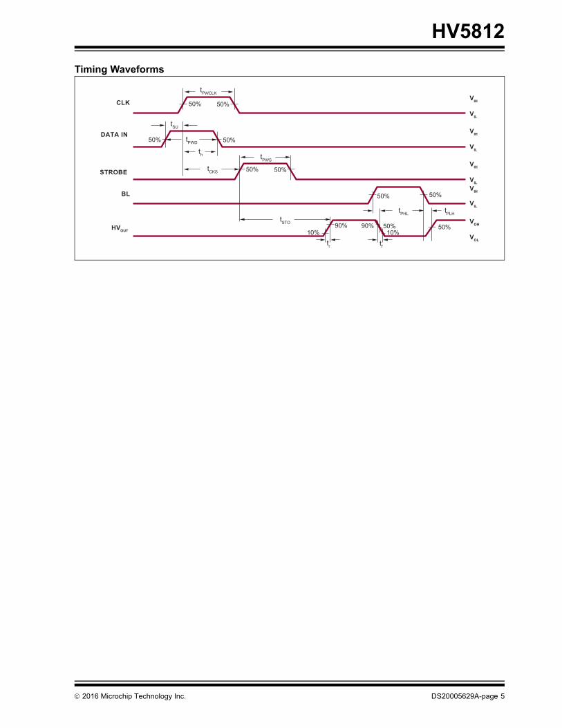
AC ELECTRICAL CHARACTERISTICS
Electrical Specifications: Over recommended operating conditions; TA = 25°C unless otherwise indicated.
Parameter Sym. Min. Typ. Max. Unit Conditions
Blanking to Output DelaytPHL — 2000 —
ns CL = 30 pF, 50% to 50%, VDD=5VtPLH — 1000 —
Output Fall Time tr — 1450 — ns CL = 30 pF, 90% to 10%, VDD = 5V
Output Rise Time tf — 650 — ns CL = 30 pF, 10% to 90%, VDD = 5V
Data Set-up Time tSU 75 — — ns See Timing Waveforms.
Data Hold Time tH 75 — — ns See Timing Waveforms.
Minimum Data Pulse Width tPWD 150 — — ns See Timing Waveforms.
Minimum Clock Pulse Width tPWCLK 150 — — ns See Timing Waveforms.
Minimum Time between Clock Activation and Strobe
tCKS 300 — — ns See Timing Waveforms.
Minimum Strobe Pulse Width tPWS 100 — — ns SeeTiming Waveforms.
Typical Time between Strobe Activation and Output Transition
tSTO — 500 — ns See Timing Waveforms.
Maximum Clock Frequency fCLK
— 8 —MHz
TJ = +25°C, VDD = 5V
— 5 — TJ = +125°C, VDD = 5V
TEMPERATURE SPECIFICATIONS
Parameter Sym. Min. Typ. Max. Unit Conditions
TEMPERATURE RANGE
Operating Junction Temperature TJ –40 — +125 °C
Storage Temperature TS –55 — +150 °C
PACKAGE THERMAL RESISTANCE
28-lead PDIP JA — 43 — °C/W
28-lead PLCC JA — 48 — °C/W
28-lead SOW JA — 55 — °C/W
DS20005629A-page 4 2016 Microchip Technology Inc.
HV5812
Timing Waveforms
CLK
DATA IN
STROBE
BL
HVOUT
tPWCLK
tPWS
tPHL
tf tr
tPLH
tSU
50%
90% 10%
50% 10%
th
tPWD
tCKS
tSTO 90%
50% 50%
50% 50%
50% 50%
VIH
VIL
VIH
VIL
VIH
VIL
VIH
VIL
VOH
VOL
50%
50%
2016 Microchip Technology Inc. DS20005629A-page 5
HV5812
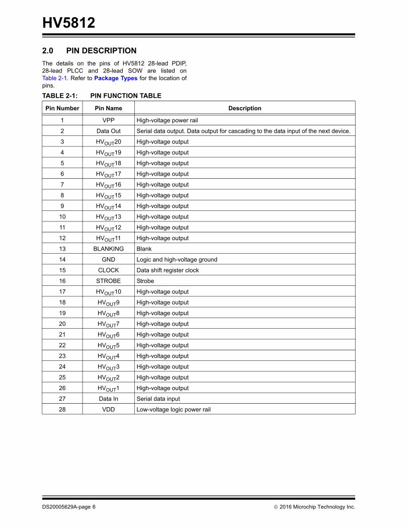
2.0 PIN DESCRIPTION
The details on the pins of HV5812 28-lead PDIP, 28-lead PLCC and 28-lead SOW are listed on Table 2-1. Refer to Package Types for the location of pins.
TABLE 2-1: PIN FUNCTION TABLE
Pin Number Pin Name Description
1 VPP High-voltage power rail
2 Data Out Serial data output. Data output for cascading to the data input of the next device.
3 HVOUT20 High-voltage output
4 HVOUT19 High-voltage output
5 HVOUT18 High-voltage output
6 HVOUT17 High-voltage output
7 HVOUT16 High-voltage output
8 HVOUT15 High-voltage output
9 HVOUT14 High-voltage output
10 HVOUT13 High-voltage output
11 HVOUT12 High-voltage output
12 HVOUT11 High-voltage output
13 BLANKING Blank
14 GND Logic and high-voltage ground
15 CLOCK Data shift register clock
16 STROBE Strobe
17 HVOUT10 High-voltage output
18 HVOUT9 High-voltage output
19 HVOUT8 High-voltage output
20 HVOUT7 High-voltage output
21 HVOUT6 High-voltage output
22 HVOUT5 High-voltage output
23 HVOUT4 High-voltage output
24 HVOUT3 High-voltage output
25 HVOUT2 High-voltage output
26 HVOUT1 High-voltage output
27 Data In Serial data input
28 VDD Low-voltage logic power rail
DS20005629A-page 6 2016 Microchip Technology Inc.

HV5812
3.0 FUNCTIONAL DESCRIPTION
Follow the steps below to power up and power down the HV5812:
POWER-UP AND POWER-DOWN SEQUENCE
Power-up Power-down
Step Description Step Description
1 Connect ground. 1 Remove VPP.
2 Apply VDD. 2 Remove all inputs.
3 Set all inputs (Data, CLK, etc.) to a known state 3 Remove VDD.
4 Apply VPP. (Note 1) 4 Disconnect ground.
Note 1: The VPP should not drop below VDD during operation.
FUNCTION TABLE (Note 1)SerialDataInput
Clock Input
Shift Register Contents SerialData
Output
Strobe Input
Latch ContentsBlanking
Output Contents
I1 I2 I3... IN-1 IN I1 I2 I3... IN-1 IN I1 I2 I3... IN-1 IN
H L to H H R1 R2...RN–2 RN–1 RN–1 — — — — — — — — — —
L L to H L R1 R2...RN–2 RN–1 RN–1 — — — — — — — — — —
X H to L R1 R2 R3...RN–1 RN RN — — — — — — — — — —
— — X X X...X X X L R1 R2 R3...RN–1 RN — — — — —
— — P1 P2 P3...PN–1 PN PN H P1 P2 P3...PN–1 PN L P1 P2 P3...PN–1 PN
— — — — — — — — X X X...X X H L L L...L L
Note 1: L = Low logic levelH = High logic levelX = Irrelevant P = Present stateR = Previous state
,
VDD
INPUT
GND
VPP
L/T
GND
HVOUT
Logic InputsGND
Data Out
Logic Data Output High Voltage Outputs
VDD
FIGURE 3-1: IO Circuits.
2016 Microchip Technology Inc. DS20005629A-page 7

HV5812
4.0 PACKAGE MARKING INFORMATION
4.1 Packaging Information
28-lead PDIP Example
HV5812Pe3
1625859 XXXXXXe3
YYWWNNN
Legend: XX...X Product Code or Customer-specific informationY Year code (last digit of calendar year)YY Year code (last 2 digits of calendar year)WW Week code (week of January 1 is week ‘01’)NNN Alphanumeric traceability code Pb-free JEDEC® designator for Matte Tin (Sn)* This package is Pb-free. The Pb-free JEDEC designator ( )
can be found on the outer packaging for this package.
Note: In the event the full Microchip part number cannot be marked on one line, it will be carried over to the next line, thus limiting the number of available characters for product code or customer-specific information. Package may or not include the corporate logo.
3e
3e
XXXXXXX e3
YYWWNNNe3HV5812WG
1678896
28-lead SOW Example
28-lead PLCC Example
XXXXXXXXXYYWWNNNe3
HV5812PJ1611231e3
DS20005629A-page 8 2016 Microchip Technology Inc.

HV5812
28-Lead PDIP (.600in Row Spacing) Package Outline (P)1.565x.580in body, .250in height (max), .100in pitch
Note 1(Index Area)
28
1
D
L A1
A A2 SeatingPlane
e
E1
D1D1
E
A
ASide View
Top View
View A - A
eAeB
b
b1
View BView B
Note:1.
Symbol A A1 A2 b b1 D D1 E E1 e eA eB L
Dimension(inches)
MIN .140* .015 .125 .014 .030 1.380 .065† .590† .485.100BSC
.600BSC
.600* .115
NOM - - - - - - - - - - -
MAX .250 .055* .195 .023† .070 1.565 .085* .625 .580 .700 .200
Drawings not to scale.
Note: For the most current package drawings, see the Microchip Packaging Specification at www.microchip.com/packaging.Note: For the most current package drawings, see the Microchip Packaging Specification at www.microchip.com/packaging.
2016 Microchip Technology Inc. DS20005629A-page 9

HV5812
28-Lead PLCC Package Outline (PJ).453x.453in. body, .180in. height (max), .050in. pitch
Symbol A A1 A2 b b1 D D1 E E1 e R
Dimension(inches)
MIN .165 .090 .062 .013 .026 .485 .450 .485 .450.050BSC
.025
NOM .172 .105 - - - .490 .453 .490 .453 .035
MAX .180 .120 .083 .021 .032 .495 .456 .495 .456 .045JEDEC Registration MS-018, Variation AB, Issue A, June, 1993. Drawings not to scale.
.150 MAX
.048/.042x 45O
1
075 MAX
4 26
DD1
E1 E
Top View
View A
AA2A1
SeatingPlane
e
Note 1 (Index Area)
.056/.042x 45O
BasePlane
.020 MIN
28
b
View A
b1
Horizontal Side View
Vertical Side View
Note 2
.020max(3 Places)
R
Notes:1.
a printed indicator.2.
Note: For the most current package drawings, see the Microchip Packaging Specification at www.microchip.com/packaging.Note: For the most current package drawings, see the Microchip Packaging Specification at www.microchip.com/packaging.
DS20005629A-page 10 2016 Microchip Technology Inc.
HV5812
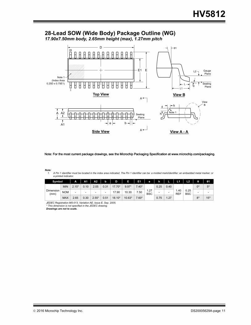
28-Lead SOW (Wide Body) Package Outline (WG)17.90x7.50mm body, 2.65mm height (max), 1.27mm pitch
Symbol A A1 A2 b D E E1 e h L L1 L2
Dimension(mm)
MIN 2.15* 0.10 2.05 0.31 17.70* 9.97* 7.40*1.27BSC
0.25 0.401.40REF
0.25BSC
0O 5O
NOM - - - - 17.90 10.30 7.50 - - - -
MAX 2.65 0.30 2.55* 0.51 18.10* 10.63* 7.60* 0.75 1.27 8O 15O
JEDEC Registration MS-013, Variation AE, Issue E, Sep. 2005.
Drawings are not to scale.S # S 28SO G 0 1309
D
SeatingPlane
GaugePlane
L
L1
L2
Top View
Side View
View B
ViewB
θ1
θ
E1 E
A A2
A1
A
A
SeatingPlane
e b
h
h
28
1
Note 1
Note 1(Index Area
0.25D x 0.75E1)
View A - A
Note:1.
a printed indicator.
Note: For the most current package drawings, see the Microchip Packaging Specification at www.microchip.com/packaging.Note: For the most current package drawings, see the Microchip Packaging Specification at www.microchip.com/packaging.
2016 Microchip Technology Inc. DS20005629A-page 11

HV5812
NOTES:
DS20005629A-page 12 2016 Microchip Technology Inc.

2016 Microchip Technology Inc. DS20005629A-page 13
HV5812
APPENDIX A: REVISION HISTORY
Revision A (October 2016)
• Converted Supertex Doc# DSFP-HV5812 to Microchip DS20005629A
• Changed the packaging quantity of 28-lead PLCC (PJ M904) from 500/Reel to 750/Reel and 28-lead SOW (WG) from 1000/Reel to 1600/Reel
• Made minor text changes throughout the docu-ment
HV5812
DS20005629A-page 14 2016 Microchip Technology Inc.
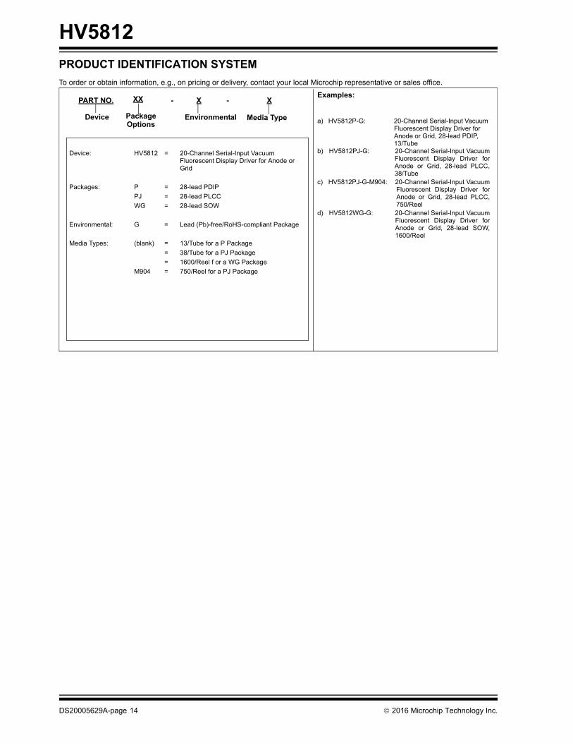
PRODUCT IDENTIFICATION SYSTEM
To order or obtain information, e.g., on pricing or delivery, contact your local Microchip representative or sales office.
Examples:
a) HV5812P-G: 20-Channel Serial-Input Vacuum Fluorescent Display Driver for Anode or Grid, 28-lead PDIP, 13/Tube
b) HV5812PJ-G: 20-Channel Serial-Input Vacuum Fluorescent Display Driver for Anode or Grid, 28-lead PLCC, 38/Tube
c) HV5812PJ-G-M904: 20-Channel Serial-Input Vacuum Fluorescent Display Driver for Anode or Grid, 28-lead PLCC, 750/Reel
d) HV5812WG-G: 20-Channel Serial-Input Vacuum Fluorescent Display Driver for Anode or Grid, 28-lead SOW, 1600/Reel
PART NO.
Device
Device: HV5812 = 20-Channel Serial-Input Vacuum Fluorescent Display Driver for Anode or Grid
Packages: P = 28-lead PDIP
PJ = 28-lead PLCC
WG = 28-lead SOW
Environmental: G = Lead (Pb)-free/RoHS-compliant Package
Media Types: (blank) = 13/Tube for a P Package
= 38/Tube for a PJ Package
= 1600/Reel f or a WG Package
M904 = 750/Reel for a PJ Package
XX
Package
- X - X
Environmental Media Type Options

Note the following details of the code protection feature on Microchip devices:
• Microchip products meet the specification contained in their particular Microchip Data Sheet.
• Microchip believes that its family of products is one of the most secure families of its kind on the market today, when used in the intended manner and under normal conditions.
• There are dishonest and possibly illegal methods used to breach the code protection feature. All of these methods, to our knowledge, require using the Microchip products in a manner outside the operating specifications contained in Microchip’s Data Sheets. Most likely, the person doing so is engaged in theft of intellectual property.
• Microchip is willing to work with the customer who is concerned about the integrity of their code.
• Neither Microchip nor any other semiconductor manufacturer can guarantee the security of their code. Code protection does not mean that we are guaranteeing the product as “unbreakable.”
Code protection is constantly evolving. We at Microchip are committed to continuously improving the code protection features of our products. Attempts to break Microchip’s code protection feature may be a violation of the Digital Millennium Copyright Act. If such acts allow unauthorized access to your software or other copyrighted work, you may have a right to sue for relief under that Act.
Information contained in this publication regarding device applications and the like is provided only for your convenience and may be superseded by updates. It is your responsibility to ensure that your application meets with your specifications. MICROCHIP MAKES NO REPRESENTATIONS OR WARRANTIES OF ANY KIND WHETHER EXPRESS OR IMPLIED, WRITTEN OR ORAL, STATUTORY OR OTHERWISE, RELATED TO THE INFORMATION, INCLUDING BUT NOT LIMITED TO ITS CONDITION, QUALITY, PERFORMANCE, MERCHANTABILITY OR FITNESS FOR PURPOSE. Microchip disclaims all liability arising from this information and its use. Use of Microchip devices in life support and/or safety applications is entirely at the buyer’s risk, and the buyer agrees to defend, indemnify and hold harmless Microchip from any and all damages, claims, suits, or expenses resulting from such use. No licenses are conveyed, implicitly or otherwise, under any Microchip intellectual property rights unless otherwise stated.
2016 Microchip Technology Inc.
Microchip received ISO/TS-16949:2009 certification for its worldwide headquarters, design and wafer fabrication facilities in Chandler and Tempe, Arizona; Gresham, Oregon and design centers in California and India. The Company’s quality system processes and procedures are for its PIC® MCUs and dsPIC® DSCs, KEELOQ® code hopping devices, Serial EEPROMs, microperipherals, nonvolatile memory and analog products. In addition, Microchip’s quality system for the design and manufacture of development systems is ISO 9001:2000 certified.
QUALITYMANAGEMENTSYSTEMCERTIFIEDBYDNV
== ISO/TS16949==
Trademarks
The Microchip name and logo, the Microchip logo, AnyRate, dsPIC, FlashFlex, flexPWR, Heldo, JukeBlox, KeeLoq, KeeLoq logo, Kleer, LANCheck, LINK MD, MediaLB, MOST, MOST logo, MPLAB, OptoLyzer, PIC, PICSTART, PIC32 logo, RightTouch, SpyNIC, SST, SST Logo, SuperFlash and UNI/O are registered trademarks of Microchip Technology Incorporated in the U.S.A. and other countries.
ClockWorks, The Embedded Control Solutions Company, ETHERSYNCH, Hyper Speed Control, HyperLight Load, IntelliMOS, mTouch, Precision Edge, and QUIET-WIRE are registered trademarks of Microchip Technology Incorporated in the U.S.A.
Analog-for-the-Digital Age, Any Capacitor, AnyIn, AnyOut, BodyCom, chipKIT, chipKIT logo, CodeGuard, dsPICDEM, dsPICDEM.net, Dynamic Average Matching, DAM, ECAN, EtherGREEN, In-Circuit Serial Programming, ICSP, Inter-Chip Connectivity, JitterBlocker, KleerNet, KleerNet logo, MiWi, motorBench, MPASM, MPF, MPLAB Certified logo, MPLIB, MPLINK, MultiTRAK, NetDetach, Omniscient Code Generation, PICDEM, PICDEM.net, PICkit, PICtail, PureSilicon, RightTouch logo, REAL ICE, Ripple Blocker, Serial Quad I/O, SQI, SuperSwitcher, SuperSwitcher II, Total Endurance, TSHARC, USBCheck, VariSense, ViewSpan, WiperLock, Wireless DNA, and ZENA are trademarks of Microchip Technology Incorporated in the U.S.A. and other countries.
SQTP is a service mark of Microchip Technology Incorporated in the U.S.A.
Silicon Storage Technology is a registered trademark of Microchip Technology Inc. in other countries.
GestIC is a registered trademarks of Microchip Technology Germany II GmbH & Co. KG, a subsidiary of Microchip Technology Inc., in other countries.
All other trademarks mentioned herein are property of their respective companies.
© 2016, Microchip Technology Incorporated, Printed in the U.S.A., All Rights Reserved.
ISBN: 978-1-5224-0999-1
DS20005629A-page 15

DS20005629A-page 16 2016 Microchip Technology Inc.
AMERICASCorporate Office2355 West Chandler Blvd.Chandler, AZ 85224-6199Tel: 480-792-7200 Fax: 480-792-7277Technical Support: http://www.microchip.com/supportWeb Address: www.microchip.com
AtlantaDuluth, GA Tel: 678-957-9614 Fax: 678-957-1455
Austin, TXTel: 512-257-3370
BostonWestborough, MA Tel: 774-760-0087 Fax: 774-760-0088
ChicagoItasca, IL Tel: 630-285-0071 Fax: 630-285-0075
ClevelandIndependence, OH Tel: 216-447-0464 Fax: 216-447-0643
DallasAddison, TX Tel: 972-818-7423 Fax: 972-818-2924
DetroitNovi, MI Tel: 248-848-4000
Houston, TX Tel: 281-894-5983
IndianapolisNoblesville, IN Tel: 317-773-8323Fax: 317-773-5453
Los AngelesMission Viejo, CA Tel: 949-462-9523 Fax: 949-462-9608
New York, NY Tel: 631-435-6000
San Jose, CA Tel: 408-735-9110
Canada - TorontoTel: 905-695-1980 Fax: 905-695-2078
ASIA/PACIFICAsia Pacific OfficeSuites 3707-14, 37th FloorTower 6, The GatewayHarbour City, Kowloon
Hong KongTel: 852-2943-5100Fax: 852-2401-3431
Australia - SydneyTel: 61-2-9868-6733Fax: 61-2-9868-6755
China - BeijingTel: 86-10-8569-7000 Fax: 86-10-8528-2104
China - ChengduTel: 86-28-8665-5511Fax: 86-28-8665-7889
China - ChongqingTel: 86-23-8980-9588Fax: 86-23-8980-9500
China - DongguanTel: 86-769-8702-9880
China - GuangzhouTel: 86-20-8755-8029
China - HangzhouTel: 86-571-8792-8115 Fax: 86-571-8792-8116
China - Hong Kong SARTel: 852-2943-5100 Fax: 852-2401-3431
China - NanjingTel: 86-25-8473-2460Fax: 86-25-8473-2470
China - QingdaoTel: 86-532-8502-7355Fax: 86-532-8502-7205
China - ShanghaiTel: 86-21-5407-5533 Fax: 86-21-5407-5066
China - ShenyangTel: 86-24-2334-2829Fax: 86-24-2334-2393
China - ShenzhenTel: 86-755-8864-2200 Fax: 86-755-8203-1760
China - WuhanTel: 86-27-5980-5300Fax: 86-27-5980-5118
China - XianTel: 86-29-8833-7252Fax: 86-29-8833-7256
ASIA/PACIFICChina - XiamenTel: 86-592-2388138 Fax: 86-592-2388130
China - ZhuhaiTel: 86-756-3210040 Fax: 86-756-3210049
India - BangaloreTel: 91-80-3090-4444 Fax: 91-80-3090-4123
India - New DelhiTel: 91-11-4160-8631Fax: 91-11-4160-8632
India - PuneTel: 91-20-3019-1500
Japan - OsakaTel: 81-6-6152-7160 Fax: 81-6-6152-9310
Japan - TokyoTel: 81-3-6880- 3770 Fax: 81-3-6880-3771
Korea - DaeguTel: 82-53-744-4301Fax: 82-53-744-4302
Korea - SeoulTel: 82-2-554-7200Fax: 82-2-558-5932 or 82-2-558-5934
Malaysia - Kuala LumpurTel: 60-3-6201-9857Fax: 60-3-6201-9859
Malaysia - PenangTel: 60-4-227-8870Fax: 60-4-227-4068
Philippines - ManilaTel: 63-2-634-9065Fax: 63-2-634-9069
SingaporeTel: 65-6334-8870Fax: 65-6334-8850
Taiwan - Hsin ChuTel: 886-3-5778-366Fax: 886-3-5770-955
Taiwan - KaohsiungTel: 886-7-213-7828
Taiwan - TaipeiTel: 886-2-2508-8600 Fax: 886-2-2508-0102
Thailand - BangkokTel: 66-2-694-1351Fax: 66-2-694-1350
EUROPEAustria - WelsTel: 43-7242-2244-39Fax: 43-7242-2244-393
Denmark - CopenhagenTel: 45-4450-2828 Fax: 45-4485-2829
France - ParisTel: 33-1-69-53-63-20 Fax: 33-1-69-30-90-79
Germany - DusseldorfTel: 49-2129-3766400
Germany - KarlsruheTel: 49-721-625370
Germany - MunichTel: 49-89-627-144-0 Fax: 49-89-627-144-44
Italy - Milan Tel: 39-0331-742611 Fax: 39-0331-466781
Italy - VeniceTel: 39-049-7625286
Netherlands - DrunenTel: 31-416-690399 Fax: 31-416-690340
Poland - WarsawTel: 48-22-3325737
Spain - MadridTel: 34-91-708-08-90Fax: 34-91-708-08-91
Sweden - StockholmTel: 46-8-5090-4654
UK - WokinghamTel: 44-118-921-5800Fax: 44-118-921-5820
Worldwide Sales and Service
06/23/16